JP5766403B2 - Driving circuit and driving method for liquid crystal display - Google Patents
Driving circuit and driving method for liquid crystal display Download PDFInfo
- Publication number
- JP5766403B2 JP5766403B2 JP2010072472A JP2010072472A JP5766403B2 JP 5766403 B2 JP5766403 B2 JP 5766403B2 JP 2010072472 A JP2010072472 A JP 2010072472A JP 2010072472 A JP2010072472 A JP 2010072472A JP 5766403 B2 JP5766403 B2 JP 5766403B2
- Authority
- JP
- Japan
- Prior art keywords
- data
- signal
- driving chip
- liquid crystal
- crystal display
- Prior art date
- Legal status (The legal status is an assumption and is not a legal conclusion. Google has not performed a legal analysis and makes no representation as to the accuracy of the status listed.)
- Expired - Fee Related
Links
Images


Classifications
-
- G—PHYSICS
- G09—EDUCATION; CRYPTOGRAPHY; DISPLAY; ADVERTISING; SEALS
- G09G—ARRANGEMENTS OR CIRCUITS FOR CONTROL OF INDICATING DEVICES USING STATIC MEANS TO PRESENT VARIABLE INFORMATION
- G09G3/00—Control arrangements or circuits, of interest only in connection with visual indicators other than cathode-ray tubes
- G09G3/20—Control arrangements or circuits, of interest only in connection with visual indicators other than cathode-ray tubes for presentation of an assembly of a number of characters, e.g. a page, by composing the assembly by combination of individual elements arranged in a matrix no fixed position being assigned to or needed to be assigned to the individual characters or partial characters
- G09G3/34—Control arrangements or circuits, of interest only in connection with visual indicators other than cathode-ray tubes for presentation of an assembly of a number of characters, e.g. a page, by composing the assembly by combination of individual elements arranged in a matrix no fixed position being assigned to or needed to be assigned to the individual characters or partial characters by control of light from an independent source
- G09G3/36—Control arrangements or circuits, of interest only in connection with visual indicators other than cathode-ray tubes for presentation of an assembly of a number of characters, e.g. a page, by composing the assembly by combination of individual elements arranged in a matrix no fixed position being assigned to or needed to be assigned to the individual characters or partial characters by control of light from an independent source using liquid crystals
- G09G3/3611—Control of matrices with row and column drivers
-
- G—PHYSICS
- G09—EDUCATION; CRYPTOGRAPHY; DISPLAY; ADVERTISING; SEALS
- G09G—ARRANGEMENTS OR CIRCUITS FOR CONTROL OF INDICATING DEVICES USING STATIC MEANS TO PRESENT VARIABLE INFORMATION
- G09G2310/00—Command of the display device
- G09G2310/02—Addressing, scanning or driving the display screen or processing steps related thereto
- G09G2310/0264—Details of driving circuits
- G09G2310/027—Details of drivers for data electrodes, the drivers handling digital grey scale data, e.g. use of D/A converters
-
- G—PHYSICS
- G09—EDUCATION; CRYPTOGRAPHY; DISPLAY; ADVERTISING; SEALS
- G09G—ARRANGEMENTS OR CIRCUITS FOR CONTROL OF INDICATING DEVICES USING STATIC MEANS TO PRESENT VARIABLE INFORMATION
- G09G2330/00—Aspects of power supply; Aspects of display protection and defect management
- G09G2330/02—Details of power systems and of start or stop of display operation
- G09G2330/021—Power management, e.g. power saving
-
- G—PHYSICS
- G09—EDUCATION; CRYPTOGRAPHY; DISPLAY; ADVERTISING; SEALS
- G09G—ARRANGEMENTS OR CIRCUITS FOR CONTROL OF INDICATING DEVICES USING STATIC MEANS TO PRESENT VARIABLE INFORMATION
- G09G3/00—Control arrangements or circuits, of interest only in connection with visual indicators other than cathode-ray tubes
- G09G3/20—Control arrangements or circuits, of interest only in connection with visual indicators other than cathode-ray tubes for presentation of an assembly of a number of characters, e.g. a page, by composing the assembly by combination of individual elements arranged in a matrix no fixed position being assigned to or needed to be assigned to the individual characters or partial characters
- G09G3/34—Control arrangements or circuits, of interest only in connection with visual indicators other than cathode-ray tubes for presentation of an assembly of a number of characters, e.g. a page, by composing the assembly by combination of individual elements arranged in a matrix no fixed position being assigned to or needed to be assigned to the individual characters or partial characters by control of light from an independent source
- G09G3/36—Control arrangements or circuits, of interest only in connection with visual indicators other than cathode-ray tubes for presentation of an assembly of a number of characters, e.g. a page, by composing the assembly by combination of individual elements arranged in a matrix no fixed position being assigned to or needed to be assigned to the individual characters or partial characters by control of light from an independent source using liquid crystals
- G09G3/3611—Control of matrices with row and column drivers
- G09G3/3614—Control of polarity reversal in general
-
- G—PHYSICS
- G09—EDUCATION; CRYPTOGRAPHY; DISPLAY; ADVERTISING; SEALS
- G09G—ARRANGEMENTS OR CIRCUITS FOR CONTROL OF INDICATING DEVICES USING STATIC MEANS TO PRESENT VARIABLE INFORMATION
- G09G3/00—Control arrangements or circuits, of interest only in connection with visual indicators other than cathode-ray tubes
- G09G3/20—Control arrangements or circuits, of interest only in connection with visual indicators other than cathode-ray tubes for presentation of an assembly of a number of characters, e.g. a page, by composing the assembly by combination of individual elements arranged in a matrix no fixed position being assigned to or needed to be assigned to the individual characters or partial characters
- G09G3/34—Control arrangements or circuits, of interest only in connection with visual indicators other than cathode-ray tubes for presentation of an assembly of a number of characters, e.g. a page, by composing the assembly by combination of individual elements arranged in a matrix no fixed position being assigned to or needed to be assigned to the individual characters or partial characters by control of light from an independent source
- G09G3/36—Control arrangements or circuits, of interest only in connection with visual indicators other than cathode-ray tubes for presentation of an assembly of a number of characters, e.g. a page, by composing the assembly by combination of individual elements arranged in a matrix no fixed position being assigned to or needed to be assigned to the individual characters or partial characters by control of light from an independent source using liquid crystals
- G09G3/3611—Control of matrices with row and column drivers
- G09G3/3685—Details of drivers for data electrodes
- G09G3/3688—Details of drivers for data electrodes suitable for active matrices only
-
- G—PHYSICS
- G09—EDUCATION; CRYPTOGRAPHY; DISPLAY; ADVERTISING; SEALS
- G09G—ARRANGEMENTS OR CIRCUITS FOR CONTROL OF INDICATING DEVICES USING STATIC MEANS TO PRESENT VARIABLE INFORMATION
- G09G3/00—Control arrangements or circuits, of interest only in connection with visual indicators other than cathode-ray tubes
- G09G3/20—Control arrangements or circuits, of interest only in connection with visual indicators other than cathode-ray tubes for presentation of an assembly of a number of characters, e.g. a page, by composing the assembly by combination of individual elements arranged in a matrix no fixed position being assigned to or needed to be assigned to the individual characters or partial characters
- G09G3/34—Control arrangements or circuits, of interest only in connection with visual indicators other than cathode-ray tubes for presentation of an assembly of a number of characters, e.g. a page, by composing the assembly by combination of individual elements arranged in a matrix no fixed position being assigned to or needed to be assigned to the individual characters or partial characters by control of light from an independent source
- G09G3/36—Control arrangements or circuits, of interest only in connection with visual indicators other than cathode-ray tubes for presentation of an assembly of a number of characters, e.g. a page, by composing the assembly by combination of individual elements arranged in a matrix no fixed position being assigned to or needed to be assigned to the individual characters or partial characters by control of light from an independent source using liquid crystals
- G09G3/3611—Control of matrices with row and column drivers
- G09G3/3696—Generation of voltages supplied to electrode drivers
Description
本発明は、液晶ディスプレーの製造分野に係り、特に液晶ディスプレーの駆動回路および駆動方法に係る。 The present invention relates to a manufacturing field of a liquid crystal display, and more particularly to a driving circuit and a driving method of a liquid crystal display.
液晶ディスプレーの製造分野において、大画面でかつ高解像度の液晶ディスプレーは、ますます広範に応用されている。大画面でかつ高解像度の液晶ディスプレーのリフレシュレートは、一般的に120Hz以上である。 In the field of manufacturing liquid crystal displays, large-screen and high-resolution liquid crystal displays are increasingly being applied. The refresh rate of a large-screen and high-resolution liquid crystal display is generally 120 Hz or higher.
液晶ディスプレーのデータ駆動チップは、それぞれ液晶ディスプレーパネルの両端に位置する。すなわち、データ駆動チップは、液晶ディスプレーパネルの上部に位置するデータ駆動チップと、液晶ディスプレーパネルの下部に位置するデータ駆動チップとを備えることができる。従来技術では、上部のデータ駆動チップと下部のデータ駆動チップとによって交替でデータ駆動を行う方法が採用される。例えば、奇数フレームに対しては、上部のデータ駆動チップから当該フレームにおける各画素に画素電圧信号を出力し、偶数フレームに対しては、下部のデータ駆動チップから当該フレームにおける各画素に画素電圧信号を出力することができる。こうして、液晶ディスプレーパネルのデータ駆動を実現する。画素電圧信号の極性反転駆動方式は、点反転駆動方式および列反転駆動方式などを含む。上述の二つの駆動方式に関して、従来技術のデータ駆動方法では、上部および下部のデータ駆動チップが出力した画素電圧信号は、いずれも正極性画素電圧信号および負極性画素電圧信号を含むため、各データ駆動チップが出力した画素電圧信号の電圧範囲はいずれも大きい。 Data driving chips of the liquid crystal display are located at both ends of the liquid crystal display panel, respectively. That is, the data driving chip may include a data driving chip located at the upper part of the liquid crystal display panel and a data driving chip located at the lower part of the liquid crystal display panel. In the prior art, a method of alternately driving data by using an upper data driving chip and a lower data driving chip is employed. For example, for an odd frame, a pixel voltage signal is output from the upper data driving chip to each pixel in the frame, and for an even frame, a pixel voltage signal is output from the lower data driving chip to each pixel in the frame. Can be output. Thus, data driving of the liquid crystal display panel is realized. The polarity inversion driving method of the pixel voltage signal includes a point inversion driving method and a column inversion driving method. Regarding the above two driving methods, in the conventional data driving method, the pixel voltage signals output from the upper and lower data driving chips both include a positive pixel voltage signal and a negative pixel voltage signal. The voltage range of the pixel voltage signal output from the driving chip is large.
ただし、点反転駆動方式は、フリッカー(flicker)およびクロストーク(crosstalk)などの不良現象を減少させ、優れた画像表示品質を得ることができるため、液晶ディスプレー分野において広範に応用されている。しかし、点反転駆動方式が、リフレシュレートの高い大画面でかつ高解像度の液晶ディスプレーに応用された場合、データ駆動チップが出力しなければならない画素電圧信号の電圧範囲は更に大きくなるため、データ駆動チップの消費電力が大きすぎるという問題が生じる。上述の、点反転駆動方式による消費電力が大きすぎるという問題を解決するために、各メーカーは普通、大画面でかつ高解像度の液晶ディスプレーを製造する際に、列反転駆動方式を採用している。列反転駆動方式で出力された画素電圧信号の電圧範囲は、点反転駆動方式よりも小さいため、データ駆動チップの消費電力をある程度に減らすことで、従来のデータ駆動チップを大画面でかつ高解像度の液晶ディスプレーに応用することができる。しかし、列反転駆動方式の場合、フリッカーおよびクロストークという二つの不良現象はいずれも著しく、画像表示品質が低下する。上述の二つの不良現象を回避して画像表示品質を向上するために、各メーカーは、アレイ(Array)基板の設計を変更しなければいけない。 However, the point inversion driving method is widely applied in the liquid crystal display field because it can reduce defective phenomena such as flicker and crosstalk and obtain excellent image display quality. However, when the point inversion driving method is applied to a large-screen and high-resolution liquid crystal display with a high refresh rate, the voltage range of the pixel voltage signal that must be output by the data driving chip is further increased. The problem arises that the power consumption of the chip is too large. In order to solve the above-described problem that the power consumption by the point inversion driving method is too large, each manufacturer usually adopts the column inversion driving method when manufacturing a large-screen and high-resolution liquid crystal display. . Since the voltage range of the pixel voltage signal output by the column inversion driving method is smaller than that of the point inversion driving method, the power consumption of the data driving chip is reduced to some extent, so that the conventional data driving chip has a large screen and high resolution. It can be applied to LCD displays. However, in the case of the column inversion driving method, both of the two defect phenomena, flicker and crosstalk, are remarkable and the image display quality is deteriorated. In order to avoid the above-described two defective phenomena and improve the image display quality, each manufacturer has to change the design of the array substrate.
従って、以上から分かるように、従来技術では、従来のデータ駆動チップを使用する場合、データ駆動チップの消費電力を有効に減らす技術案がない。 Therefore, as can be seen from the above, in the conventional technology, there is no technical solution for effectively reducing the power consumption of the data driving chip when the conventional data driving chip is used.
本発明は、従来技術における問題点に対して、従来のデータ駆動チップを使用する場合にデータ駆動チップの消費電力を有効に減らすという課題を解決する液晶ディスプレーの駆動回路および駆動方法を提供することを目的とする。 The present invention provides a driving circuit and a driving method for a liquid crystal display that solves the problem of effectively reducing the power consumption of a data driving chip when a conventional data driving chip is used. With the goal.
上述の目的を実現するために、本発明は、シーケンス制御器と、前記シーケンス制御器に接続される第1のデータ駆動チップおよび第2のデータ駆動チップと、前記第1のデータ駆動チップおよび前記第2のデータ駆動チップにそれぞれ接続される参照電圧バッファーと、を備える液晶ディスプレーの駆動回路を提供する。 To achieve the above object, the present invention provides a sequence controller, a first data driving chip and a second data driving chip connected to the sequence controller, the first data driving chip, and the Provided is a liquid crystal display driving circuit including a reference voltage buffer connected to each of second data driving chips.
前記シーケンス制御器は、受信した低電圧差分信号を復号してデータ表示信号とシーケンス制御信号とを生成し、前記シーケンス制御信号に基づいて、前記データ表示信号を第1のデータ表示信号と第2のデータ表示信号とに分け、前記第1のデータ表示信号を前記第1のデータ駆動チップに送信し、前記第2のデータ表示信号を前記第2のデータ駆動チップに送信し、前記シーケンス制御信号をそれぞれ前記第1のデータ駆動チップと前記第2のデータ駆動チップに送信する。 The sequence controller decodes the received low voltage difference signal to generate a data display signal and a sequence control signal, and based on the sequence control signal, the data display signal is converted into a first data display signal and a second data display signal. And the first data display signal is transmitted to the first data driving chip, the second data display signal is transmitted to the second data driving chip, and the sequence control signal is transmitted to the second data driving chip. Are transmitted to the first data driving chip and the second data driving chip, respectively.
前記参照電圧バッファーは、第1の参照電圧と第2の参照電圧とを生成し、前記第1の参照電圧を前記第1のデータ駆動チップに送信するとともに、前記第2の参照電圧を前記第2のデータ駆動チップに送信する。 The reference voltage buffer generates a first reference voltage and a second reference voltage, transmits the first reference voltage to the first data driving chip, and transmits the second reference voltage to the first data driving chip. Send to 2 data driven chips.
前記第1のデータ駆動チップと前記第2のデータ駆動チップとは、フレームを間隔として液晶ディスプレーパネルの同一画素に対して交替駆動を行い、前記第1のデータ駆動チップは、前記第1の参照電圧と前記シーケンス制御信号とに基づいて、前記第1のデータ表示信号を処理して、負極性画素電圧信号を生成して前記液晶ディスプレーパネルに出力し、前記第2のデータ駆動チップは、前記第2の参照電圧と前記シーケンス制御信号とに基づいて、前記第2のデータ表示信号を処理して、正極性画素電圧信号を生成して前記液晶ディスプレーパネルに出力し、前記負極性画素電圧信号は、前記液晶ディスプレーパネルの共通電圧信号よりも低く、前記正極性画素電圧信号は、前記液晶ディスプレーパネルの共通電圧信号よりも高い。 The first data driving chip and the second data driving chip perform alternate driving on the same pixel of the liquid crystal display panel with a frame as an interval, and the first data driving chip is the first reference Based on the voltage and the sequence control signal, the first data display signal is processed, a negative pixel voltage signal is generated and output to the liquid crystal display panel, and the second data driving chip is Based on the second reference voltage and the sequence control signal, the second data display signal is processed to generate a positive pixel voltage signal and output it to the liquid crystal display panel, and the negative pixel voltage signal Is lower than the common voltage signal of the liquid crystal display panel, and the positive pixel voltage signal is higher than the common voltage signal of the liquid crystal display panel.
上述の目的を実現するために、本発明は液晶ディスプレーの駆動方法を提供する。この方法は、
シーケンス制御器が、受信した低電圧差分信号を復号してデータ表示信号とシーケンス制御信号とを生成するステップ1と、
シーケンス制御器が、前記シーケンス制御信号に基づいて、前記データ表示信号を第1のデータ表示信号と第2のデータ表示信号に分け、前記第1のデータ表示信号を前記第1のデータ駆動チップに送信し、前記第2のデータ表示信号を前記第2のデータ駆動チップに送信するとともに、前記シーケンス制御信号をそれぞれ前記第1のデータ駆動チップと前記第2のデータ駆動チップとに送信するステップ2と、
前記第1のデータ駆動チップと前記第2のデータ駆動チップとは、フレームを間隔として液晶ディスプレーパネルの同一画素に対して交替駆動を行い、前記第1のデータ駆動チップは、参照電圧バッファーが提供した第1の参照電圧と前記シーケンス制御信号とに基づいて、前記第1のデータ表示信号を処理し、負極性画素電圧信号を生成して前記液晶ディスプレーパネルに出力し、前記第2のデータ駆動チップは、参照電圧バッファーが提供した第2の参照電圧と前記シーケンス制御信号とに基づいて、前記第2のデータ表示信号を処理し、正極性画素電圧信号を生成して前記液晶ディスプレーパネルに出力するステップ3と、を含み、
前記負極性画素電圧信号は前記液晶ディスプレーパネルの共通電圧信号よりも低く、前記正極性画素電圧信号は、前記液晶ディスプレーパネルの共通電圧信号よりも高い。
In order to achieve the above object, the present invention provides a method for driving a liquid crystal display. This method
A sequence controller divides the data display signal into a first data display signal and a second data display signal based on the sequence control signal, and the first data display signal is supplied to the first data driving chip. Transmitting, transmitting the second data display signal to the second data driving chip, and transmitting the sequence control signal to the first data driving chip and the second data driving chip, respectively. When,
The first data driving chip and the second data driving chip perform alternate driving on the same pixel of the liquid crystal display panel with a frame as an interval, and the first data driving chip is provided by a reference voltage buffer Based on the first reference voltage and the sequence control signal, the first data display signal is processed, a negative pixel voltage signal is generated and output to the liquid crystal display panel, and the second data driving The chip processes the second data display signal based on the second reference voltage provided by the reference voltage buffer and the sequence control signal, generates a positive pixel voltage signal, and outputs it to the liquid crystal display panel. Including
The negative pixel voltage signal is lower than the common voltage signal of the liquid crystal display panel, and the positive pixel voltage signal is higher than the common voltage signal of the liquid crystal display panel.
本発明における二つのデータ駆動チップは、それぞれ液晶ディスプレーパネルに正極性画素電圧信号と負極性画素電圧信号とを出力する。従来技術において各データ駆動チップがいずれも正極性画素電圧信号と負極性画素電圧信号とを出力する必要があることに対して、本発明は各データ駆動チップが出力した画素電圧信号の電圧範囲を有効に縮小するため、従来のデータ駆動チップを使用する場合にデータ駆動チップの消費電力を有効に減らす。 The two data driving chips in the present invention each output a positive pixel voltage signal and a negative pixel voltage signal to the liquid crystal display panel. In the prior art, each data driving chip needs to output a positive pixel voltage signal and a negative pixel voltage signal, whereas the present invention limits the voltage range of the pixel voltage signal output by each data driving chip. In order to reduce the size effectively, the power consumption of the data driving chip is effectively reduced when the conventional data driving chip is used.
以下、本発明の技術案を図および実施例に基づいて詳細に説明する。 Hereinafter, the technical solution of the present invention will be described in detail based on the drawings and examples.
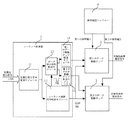
図1は本発明の液晶ディスプレーの駆動回路の実施例の構成概略図である。図1に示されているように、この駆動回路は、シーケンス制御器1と、シーケンス制御器1に接続される第1のデータ駆動チップ2および第2のデータ駆動チップ3と、第1のデータ駆動チップ2および第2のデータ駆動チップ3のそれぞれに接続される参照電圧バッファー4と、を備える。
FIG. 1 is a schematic configuration diagram of an embodiment of a driving circuit for a liquid crystal display according to the present invention. As shown in FIG. 1, the driving circuit includes a
シーケンス制御器1は、受信した低電圧差分信号を復号してデータ表示信号およびシーケンス制御信号を生成する。シーケンス制御器1は、シーケンス制御信号に基づいて、データ表示信号を第1のデータ表示信号と第2のデータ表示信号とに分け、第1のデータ表示信号を第1のデータ駆動チップ2に送信し、第2のデータ表示信号を第2のデータ駆動チップ3に送信し、シーケンス制御信号を第1のデータ駆動チップ2と第2のデータ駆動チップ3とに送信する。参照電圧バッファー4は、第1の参照電圧と第2の参照電圧とを生成し、第1の参照電圧を第1のデータ駆動チップ2に送信し、第2の参照電圧を第2のデータ駆動チップ3に送信する。第1のデータ駆動チップ2は、第1の参照電圧とシーケンス制御信号に基づいて、第1のデータ表示信号を処理し負極性画素電圧信号を生成して液晶ディスプレーパネルに出力し、第2のデータ駆動チップ3は、第2の参照電圧とシーケンス制御信号とに基づいて、第2のデータ表示信号を処理し、正極性画素電圧信号を生成して液晶ディスプレーパネルに出力する。負極性画素電圧信号は、液晶ディスプレーパネルの共通電圧信号よりも低く、正極性画素電圧信号は、液晶ディスプレーパネルの共通電圧信号よりも高い。
The
本実施例において、シーケンス制御信号は、極性反転信号(POL信号と略称する)とデータ読取および出力信号(LOAD信号と略称する)とを備えることができる。具体的には、シーケンス制御器1は、POL信号に基づいてデータ表示信号を第1のデータ表示信号と第2のデータ表示信号とに分ける。
In this embodiment, the sequence control signal can include a polarity inversion signal (abbreviated as POL signal) and a data read and output signal (abbreviated as LOAD signal). Specifically, the
本実施例において、第1の参照電圧は、GAMMA10〜GAMMA18の値を取ることができ、第2の参照電圧は、GAMMA1〜GAMMA9の値を取ることができる。第1の参照電圧がGAMMA10〜GAMMA18の値を取る場合、第1のデータ駆動チップ2は、負極性画素電圧信号を生成し、第2の参照電圧がGAMMA1〜GAMMA9の値を取る場合、第2のデータ駆動チップ3は、正極性画素電圧信号を生成する。
In the present embodiment, the first reference voltage can take values of GAMMA10 to GAMMA18, and the second reference voltage can take values of GAMMA1 to GAMMA9. When the first reference voltage takes a value of GAMMA10 to GAMMA18, the first
具体的には、シーケンス制御器1は、低電圧差分信号受信モジュール11と、低電圧差分信号受信モジュール11に接続されるデータ表示信号転送モジュール12と、低電圧差分信号受信モジュール11に接続されるシーケンス制御信号転送モジュール13と、データ表示信号転送モジュール12に接続される第1のデータ駆動チップ転送モジュール14と、データ表示信号転送モジュール12に接続される第2のデータ駆動チップ転送モジュール15と、を備える。第1のデータ駆動チップ転送モジュール14は、更に第1のデータ駆動チップ2に接続され、第2のデータ駆動チップ転送モジュール15は、更に第2のデータ駆動チップ3に接続され、シーケンス制御信号転送モジュール13は、更にそれぞれ第1のデータ駆動チップ2および第2のデータ駆動チップ3に接続される。低電圧差分信号受信モジュール11は、低電圧差分信号を受信し、低電圧差分信号を復号してデータ表示信号とシーケンス制御信号とを生成し、データ表示信号をデータ表示信号転送モジュール12に送信し、シーケンス制御信号をシーケンス制御信号転送モジュール13に送信する。シーケンス制御信号転送モジュール13は、シーケンス制御信号をそれぞれ第1のデータ駆動チップ2と第2のデータ駆動チップ3とに送信するとともに、シーケンス制御信号をデータ表示信号転送モジュール12に送信する。データ表示信号転送モジュール12は、シーケンス制御信号に基づいて、データ表示信号を第1のデータ表示信号と第2のデータ表示信号とに分け、具体的には、シーケンス制御信号における極性反転信号に基づいてデータ表示信号を第1のデータ表示信号と第2のデータ表示信号とに分け、かつ第1のデータ表示信号を第1のデータ駆動チップ転送モジュール14に送信し、第2のデータ表示信号を第2のデータ駆動チップ転送モジュール15に送信する。第1のデータ駆動チップ転送モジュール14は、第1のデータ表示信号を第1のデータ駆動チップ2に転送し、第2のデータ駆動チップ転送モジュール15は、第2のデータ表示信号を第2のデータ駆動チップ3に転送する。
Specifically, the
図2は、本発明の第1のデータ駆動チップの構成概略図である。図2に示されているように、具体的には以下のとおりである。第1のデータ駆動チップ2は、第1のデータ表示信号受信器21と、第1のデータ表示信号受信器21に接続される第1のデータラッチ22と、第1のデータラッチ22に接続される第1の抵抗型デジタル/アナログ変換器23と、第1の抵抗型デジタル/アナログ変換器23に接続される第1の出力バッファー24と、第1の出力バッファーと24に接続される第1の出力スイッチ25と、を備える。第1のデータ表示信号受信器21は、第1のデータ表示信号を受信し、第1のデータ表示信号を第1のデータラッチ22に送信する。第1のデータラッチ22は、受信したシーケンス制御信号に基づいて、第1のデータ表示信号に対してラッチ処理を行い、具体的には、受信したシーケンス制御信号におけるLOAD信号に基づいて第1のデータ表示信号に対してラッチ処理を行う。第1の抵抗型デジタル/アナログ変換器23は、受信した第1の参照電圧に基づいて、ラッチ処理された第1のデータ表示信号に対してデジタル/アナログ変換を行って負極性画素電圧信号を生成する。第1の出力バッファー24は、受信したシーケンス制御信号に基づいて負極性画素電圧信号に対してバッファー処理を行い、具体的には、受信したシーケンス制御信号におけるLOAD信号に基づいて負極性画素電圧信号に対してバッファー処理を行う。第1の出力スイッチ25は、シーケンス制御信号に基づいて負極性画素電圧信号を液晶ディスプレーパネルに出力し、具体的には、シーケンス制御信号における極性反転信号に基づいて負極性画素電圧信号を液晶ディスプレーパネルに出力する。第1の出力スイッチ25が、極性反転信号に基づいて負極性画素電圧信号を液晶ディスプレーパネルに出力することは、具体的には、液晶ディスプレーパネルのある行のゲートラインがターンオンされたときに、第1の出力スイッチ25が極性反転信号に基づいて液晶ディスプレーパネルのデータラインのオン/オフを制御し、オンされたデータラインを介して当該オンされたデータラインと対応した画素に負極性画素電圧信号を出力する、ということである。
FIG. 2 is a schematic configuration diagram of the first data driving chip of the present invention. Specifically, as shown in FIG. The first
図3は、本発明の第2のデータ駆動チップの構成概略図である。図3に示されているように、具体的には以下のとおりである。第2のデータ駆動チップ3は、第2のデータ表示信号受信器31と、第2のデータ表示信号受信器31に接続される第2のデータラッチ32と、第2のデータラッチ32に接続される第2の抵抗型デジタル/アナログ変換器33と、第2の抵抗型デジタル/アナログ変換器33に接続される第2の出力バッファー34と、第2の出力バッファー34に接続される第2の出力スイッチ35と、を備える。第2のデータ表示信号受信器31は、第2のデータ表示信号を受信して第2のデータラッチ32に送信する。第2のデータラッチ32は受信したシーケンス制御信号に基づいて、第2のデータ表示信号に対してラッチ処理を行い、具体的には、受信したシーケンス制御信号におけるLOAD信号に基づいて第2のデータ表示信号に対してラッチ処理を行う。第2の抵抗型デジタル/アナログ変換器33は第2の参照電圧に基づいて、第2のデータ表示信号に対してデジタル/アナログ変換を行って正極性画素電圧信号を生成する。第2の出力バッファー34は、シーケンス制御信号に基づいて正極性画素電圧信号に対してバッファー処理を行い、具体的には、シーケンス制御信号におけるLOAD信号に基づいて負極性画素電圧信号に対してバッファー処理を行う。第2の出力スイッチ35は、シーケンス制御信号に基づいて正極性画素電圧信号を液晶ディスプレーパネルに出力し、具体的には、シーケンス制御信号における極性反転信号に基づいて正極性画素電圧信号を液晶ディスプレーパネルに出力する。第2の出力スイッチ35が、極性反転信号に基づいて正極性画素電圧信号を液晶ディスプレーパネルに出力することは、具体的には、液晶ディスプレーパネルのある行のゲートラインがターンオンされたときに、第2の出力スイッチ35が極性反転信号に基づいて液晶ディスプレーパネルのデータラインのオン/オフを制御し、オンされたデータラインを介して当該オンされたデータラインと対応した画素に正極性画素電圧信号を出力する、ということである。
FIG. 3 is a schematic configuration diagram of a second data driving chip of the present invention. Specifically, as shown in FIG. The second
本実施例における液晶ディスプレー駆動回路によれば、液晶ディスプレーパネルの極性反転方式は、点反転駆動方式、列反転駆動方式、行反転駆動方式、または他の各種の反転駆動方式である。 According to the liquid crystal display driving circuit in this embodiment, the polarity inversion method of the liquid crystal display panel is a point inversion driving method, a column inversion driving method, a row inversion driving method, or other various inversion driving methods.
以下、点反転駆動方式を例として、液晶ディスプレー駆動回路の駆動過程を詳細に説明する。液晶ディスプレーの画像表示過程において、連続する二つのフレームにおける各画素の画素電圧信号の極性は、互いに対して反対である。図4は、本発明の点反転駆動方式の場合の奇数フレームにおける各画素電圧信号の極性の概略図である。図5は、本発明の点反転駆動方式の場合の偶数フレームにおける各画素電圧信号の極性の概略図である。図4および図5に示すように、図4および図5における液晶ディスプレーパネルの極性反転方式は、点反転駆動方式である。 Hereinafter, the driving process of the liquid crystal display driving circuit will be described in detail by taking the point inversion driving method as an example. In the image display process of the liquid crystal display, the polarity of the pixel voltage signal of each pixel in two consecutive frames is opposite to each other. FIG. 4 is a schematic diagram of the polarity of each pixel voltage signal in an odd frame in the case of the point inversion driving method of the present invention. FIG. 5 is a schematic diagram of the polarity of each pixel voltage signal in an even frame in the case of the point inversion driving method of the present invention. As shown in FIGS. 4 and 5, the polarity inversion method of the liquid crystal display panel in FIGS. 4 and 5 is a point inversion driving method.
このとき、シーケンス制御器1におけるデータ表示信号転送モジュール12は、極性反転信号に基づいてデータ表示信号を第1のデータ表示信号と第2のデータ表示信号とに分け、第1のデータ表示信号を第1のデータ駆動チップ転送モジュール14に送信し、第2のデータ表示信号を第2のデータ駆動チップ転送モジュール15に送信するということは、具体的には以下のとおりである。すなわち、データ表示信号転送モジュール12の受信した極性反転信号がローレベル信号である場合に、液晶ディスプレーパネルのある行の画素に対応するデータ表示信号を順に第1のデータ駆動チップ転送モジュール14と第2のデータ駆動チップ転送モジュール15とに交替で送信する。ここで、第1のデータ駆動チップ転送モジュール14に送信したのは第1のデータ表示信号であり、第2のデータ駆動チップ転送モジュール15に送信したのは第2のデータ表示信号である。データ表示信号転送モジュール12の受信した極性反転信号がハイレベル信号である場合に、液晶ディスプレーパネルのある行の画素に対応するデータ表示信号を順に第2のデータ駆動チップ転送モジュール15と第1のデータ駆動チップ転送モジュール14とに送信する。ここで、第1のデータ駆動チップ転送モジュール14に送信したのは第1のデータ表示信号であり、第2のデータ駆動チップ転送モジュール15に送信したのは第2のデータ表示信号である。液晶ディスプレーパネルの極性反転方式を点反転駆動方式とするために、液晶ディスプレーパネルにおいて隣接する行の画素のデータ表示信号に対応する極性反転信号は異なり、例えば、ある行の画素のデータ表示信号に対応する極性反転信号はローレベル信号であると、この行に隣接した行の画素のデータ表示信号に対応する極性反転信号はハイレベル信号である。図4における奇数フレームについて、このフレームの1行目の画素のデータ表示信号に対応する極性反転信号は、ローレベル信号でも良い、図5における偶数フレームについては、このフレームの1行目の画素のデータ表示信号に対応する極性反転信号は、ハイレベル信号でも良い。
At this time, the data display
第1のデータ駆動チップ2は、第1のデータ駆動チップ転送モジュール14が送信した第1のデータ表示信号を受信した後に、第1のデータ駆動チップ2における第1の抵抗型デジタル/アナログ変換器23によって数値範囲がGAMMA10〜GAMMA18の第1の参照電圧に基づいて、第1のデータ表示信号に対してデジタル/アナログ変換を行って負極性画素電圧信号を生成する。第2のデータ駆動チップ3は、第2のデータ駆動チップ転送モジュール15が送信した第2のデータ表示信号を受信した後に、第2のデータ駆動チップ3における第2の抵抗型デジタル/アナログ変換器33によって数値範囲がGAMMA1〜GAMMA9の第2の参照電圧に基づいて、第2のデータ表示信号に対してデジタル/アナログ変換を行って正極性画素電圧信号を生成する。更には、第1のデータ駆動チップ2における第1の出力スイッチ25によって極性反転信号に基づいて、負極性画素電圧信号を液晶ディスプレーパネルに出力し、第2のデータ駆動チップ3における第2の出力スイッチ35によって極性反転信号に基づいて、正極性画素電圧信号を液晶ディスプレーパネルに出力する。具体的には、図6に示すとおりである。図6は、本発明の点反転駆動方式の場合の画素電圧信号の出力概略図である。液晶ディスプレーパネルのある行のゲートラインがターンオンされたときに、極性反転信号がローレベル信号であると、第1のデータ駆動チップ2における第1の出力スイッチ25は、液晶ディスプレーパネルの奇数列データラインが第1の出力スイッチ25に対してターンオンされ、偶数列データラインが第1の出力スイッチ25に対してターンオフされるように制御し、第1のデータ駆動チップ2における第1の出力スイッチ25は、オンされた奇数列データラインを介してこのデータラインに対応する画素に負極性画素電圧信号を出力する。それとともに、第2のデータ駆動チップ3における第2の出力スイッチ35は、液晶ディスプレーパネルの偶数列データラインが第2の出力スイッチ35に対してターンオンされ、奇数列データラインが第2の出力スイッチ35に対してターンオフされるように制御し、第2のデータ駆動チップ3における第2の出力スイッチ35はオンされた偶数列データラインを介してこのデータラインに対応する画素に正極性画素電圧信号を出力する。液晶ディスプレーパネルのある行のゲートラインがターンオンされたときに、極性反転信号がハイレベル信号であると、第1のデータ駆動チップ2における第1の出力スイッチ25は、液晶ディスプレーパネルの偶数列データラインが第1の出力スイッチ25に対してターンオンされ、奇数列データラインが第1の出力スイッチ25に対してターンオフされるように制御し、第1のデータ駆動チップ2における第1の出力スイッチ25は、オンされた偶数列データラインを介してこのデータラインに対応する画素に負極性画素電圧信号を出力する。それとともに、第2のデータ駆動チップ3における第2の出力スイッチ35は、液晶ディスプレーパネルの奇数列データラインが第2の出力スイッチ35に対してターンオンされ、偶数列データラインが第2の出力スイッチ35に対してターンオフされるように制御し、第2のデータ駆動チップ3における第2の出力スイッチ35は、オンされた奇数列データラインを介してこのデータラインに対応する画素に正極性画素電圧信号を出力する。例えば、図4における奇数フレームの1行目の画素について、第1のデータ駆動チップ2は、奇数列データラインを介して奇数列画素に負極性画素電圧信号を出力し、第2のデータ駆動チップ3は、偶数列データラインを介して偶数列画素に正極性画素電圧信号を出力する。図5における偶数フレームの1行目の画素について、第1のデータ駆動チップ2は偶数列データラインを介して偶数列画素に負極性画素電圧信号を出力し、第2のデータ駆動チップ3は、奇数列データラインを介して奇数列画素に正極性画素電圧信号を出力する。このように、液晶ディスプレーパネルにおける各画素電圧信号の極性反転方式は、点反転駆動方式である。
The first
本実施例における二つのデータ駆動チップは、それぞれ液晶ディスプレーパネルに正極性画素電圧信号と負極性画素電圧信号とを出力する。従来技術における各データ駆動チップは、いずれも正極性画素電圧信号と負極性画素電圧信号とを出力する必要があることに対して、本実施例は、各データ駆動チップが出力した画素電圧信号の電圧範囲を有効に縮小するため、データ駆動チップの消費電力を有効に減らす。データ駆動チップの消費電力を有効に減らすため、本実施例における点反転駆動方式を大画面かつ高解像度の液晶ディスプレーに応用することで、更に優れた画像表示品質を得る。シーケンス制御器は、データ表示信号を二部分に分けてそれぞれ二つのデータ駆動チップに出力して、リフレシュレートを減らすため、ある程度、電磁干渉(Electromagnetic Interference、EMIと略称する)を減らす。従来技術と比べて、各データ駆動チップは、元の参照電圧範囲の半分だけが必要となるので、データ駆動チップの内部回路に対して簡素化処理を行うため、簡素化したデータ駆動チップは、画像表示品質を向上するとともに消費電力を節約することができる。 The two data driving chips in this embodiment each output a positive pixel voltage signal and a negative pixel voltage signal to the liquid crystal display panel. In contrast to the fact that each data driving chip in the prior art needs to output a positive pixel voltage signal and a negative pixel voltage signal, in this embodiment, the pixel voltage signal output by each data driving chip In order to effectively reduce the voltage range, the power consumption of the data driving chip is effectively reduced. In order to effectively reduce the power consumption of the data driving chip, the point inversion driving method in this embodiment is applied to a large-screen and high-resolution liquid crystal display, thereby obtaining even better image display quality. The sequence controller divides the data display signal into two parts and outputs the data display signals to two data driving chips, respectively, to reduce the refresh rate. Therefore, the sequence controller reduces electromagnetic interference (abbreviated as EMI) to some extent. Compared to the prior art, each data driving chip needs only half of the original reference voltage range, so that the simplified circuit for the internal circuit of the data driving chip is simplified. Image display quality can be improved and power consumption can be saved.
図7は、本発明の液晶ディスプレーの駆動方法のフローチャートである。本実施例における駆動方法は、図1における駆動回路を参照することができる。図7に示すように、この方法は以下のステップを備える。 FIG. 7 is a flowchart of the liquid crystal display driving method of the present invention. For the driving method in this embodiment, the driving circuit in FIG. 1 can be referred to. As shown in FIG. 7, the method includes the following steps.
ステップ101で、シーケンス制御器は、受信した低電圧差分信号を復号してデータ表示信号とシーケンス制御信号を生成する。
In
本実施例において、シーケンス制御信号は、極性反転信号(POL信号と略称する)とデータ読取および出力信号(LOAD信号と略称する)とに分けることができる。 In this embodiment, the sequence control signal can be divided into a polarity inversion signal (abbreviated as POL signal) and a data reading and output signal (abbreviated as LOAD signal).
ステップ102で、シーケンス制御器は、シーケンス制御信号に基づいて、データ表示信号を第1のデータ表示信号と第2のデータ表示信号とに分け、第1のデータ表示信号を第1のデータ駆動チップに送信し、第2のデータ表示信号を第2のデータ駆動チップに送信し、シーケンス制御信号をそれぞれ第1のデータ駆動チップと第2のデータ駆動チップとに送信する。 In step 102, the sequence controller divides the data display signal into the first data display signal and the second data display signal based on the sequence control signal, and the first data display signal is divided into the first data driving chip. The second data display signal is transmitted to the second data driving chip, and the sequence control signal is transmitted to the first data driving chip and the second data driving chip, respectively.
具体的には、シーケンス制御器は、POL信号に基づいてデータ表示信号を第1のデータ表示信号と第2のデータ表示信号とに分ける。 Specifically, the sequence controller divides the data display signal into a first data display signal and a second data display signal based on the POL signal.
ステップ103で、第1のデータ駆動チップと第2のデータ駆動チップとは、フレームを間隔として液晶ディスプレーパネルの同一画素に対して交替駆動を行い、第1のデータ駆動チップは、参照電圧バッファーが提供した第1の参照電圧とシーケンス制御信号とに基づいて、第1のデータ表示信号を処理して負極性画素電圧信号を生成して液晶ディスプレーパネルに出力し、第2のデータ駆動チップは、参照電圧バッファーが提供した第2の参照電圧とシーケンス制御信号とに基づいて、第2のデータ表示信号を処理して正極性画素電圧信号を生成して液晶ディスプレーパネルに出力する。負極性画素電圧信号は、液晶ディスプレーパネルの共通電圧信号よりも低く、正極性画素電圧信号は、液晶ディスプレーパネルの共通電圧信号よりも高い。
In
ステップ103は、具体的には、第1のデータ駆動チップが、第1の参照電圧に基づいて第1のデータ表示信号に対してデジタル/アナログ変換を行って負極性画素電圧信号を生成し、第1のデータ駆動チップが、シーケンス制御信号に基づいて負極性画素電圧信号を液晶ディスプレーパネルに出力するステップと、第2のデータ駆動チップが、第2の参照電圧に基づいて第2のデータ表示信号に対してデジタル/アナログ変換を行って正極性画素電圧信号を生成し、第2のデータ駆動チップがシーケンス制御信号に基づいて正極性画素電圧信号を液晶ディスプレーパネルに出力するステップと、を含む。第1のデータ駆動チップが、シーケンス制御信号に基づいて、負極性画素電圧信号を前記液晶ディスプレーパネルに出力するステップは、具体的には、液晶ディスプレーパネルのある行のゲートラインがターンオンされた時に、第1のデータ駆動チップが極性反転信号に基づいて液晶ディスプレーパネルのデータラインの第1のデータ駆動チップに対するオン/オフを制御し、オンされたデータラインを介してこのオンされたデータラインに対応する画素に負極性画素電圧信号を出力するステップを含む。第2のデータ駆動チップが、シーケンス制御信号に基づいて、正極性画素電圧信号を液晶ディスプレーパネルを出力するステップは、具体的には、液晶ディスプレーパネルのある行のゲートラインがターンオンされた時に、第2のデータ駆動チップは極性反転信号に基づいて液晶ディスプレーパネルのデータラインの第2のデータ駆動チップに対するオン/オフを制御し、オンされたデータラインを介してこのオンされたデータラインに対応する画素に正極性画素電圧信号を出力することを備える。第1のデータ駆動チップと第2のデータ駆動チップとは、フレームを間隔として液晶ディスプレーパネルの同一画素に対して交替駆動を行うため、あるデータラインが第1のデータ駆動チップに対してオンされたときに、このデータラインは第2データ駆動チップに対してオフされる。
In
更には、第1のデータ駆動チップが、第1の参照電圧に基づいて第1のデータ表示信号に対してデジタル/アナログ変換を行って負極性画素電圧信号を生成する前には、更に、第1のデータ駆動チップが、LOAD信号に基づいて受信した第1のデータ表示信号に対してラッチ処理を行うステップを含む。第1のデータ駆動チップが、シーケンス制御信号に基づいて負極性画素電圧信号を前記液晶ディスプレーパネルに出力する前には、更に第1のデータ駆動チップが、LOAD信号に基づいて負極性画素電圧信号に対してバッファー処理を行うステップを含む。第2のデータ駆動チップが、第2の参照電圧に基づいて第2のデータ表示信号に対してデジタル/アナログ変換を行って正極性画素電圧信号を生成する前には、更に第2のデータ駆動チップが、LOAD信号に基づいて受信した第2のデータ表示信号に対してラッチ処理を行うステップを含む。第2のデータ駆動チップが、シーケンス制御信号に基づいて、正極性画素電圧信号を前記液晶ディスプレーパネルに出力をする前には、更に第2のデータ駆動チップが、LOAD信号に基づいて正極性画素電圧信号に対してバッファー処理を行うステップを含む。 Further, before the first data driving chip performs the digital / analog conversion on the first data display signal based on the first reference voltage to generate the negative pixel voltage signal, One data driving chip includes a step of latching the first data display signal received based on the LOAD signal. Before the first data driving chip outputs a negative pixel voltage signal to the liquid crystal display panel based on the sequence control signal, the first data driving chip further performs a negative pixel voltage signal based on the LOAD signal. Including a step of performing buffer processing on. Before the second data driving chip generates a positive pixel voltage signal by performing digital / analog conversion on the second data display signal based on the second reference voltage, the second data driving chip The chip includes a step of latching the second data display signal received based on the LOAD signal. Before the second data driving chip outputs the positive pixel voltage signal to the liquid crystal display panel based on the sequence control signal, the second data driving chip further detects the positive pixel based on the LOAD signal. Buffering the voltage signal.
本実施例における液晶ディスプレーの駆動方法によれば、液晶ディスプレーパネルの極性反転方式は、点反転駆動方式、列反転駆動方式、または行反転駆動方式であることが可能である。 According to the liquid crystal display driving method in this embodiment, the polarity inversion method of the liquid crystal display panel can be a point inversion driving method, a column inversion driving method, or a row inversion driving method.
本実施例における二つのデータ駆動チップは、それぞれ液晶ディスプレーパネルに正極性画素電圧信号と負極性画素電圧信号とを出力する。従来技術における各データ駆動チップは、いずれも正極性画素電圧信号と負極性画素電圧信号とを出力する必要があるのに対して、本実施例は、各データ駆動チップが出力した画素電圧信号の電圧範囲を有効に縮小するため、データ駆動チップの消費電力を有効に減らす。データ駆動チップの消費電力を有効に減らすため、本実施例における点反転駆動方式が大画面かつ高解像度の液晶ディスプレーに応用されることで、更に優れた画像表示品質を得る。シーケンス制御器は、データ表示信号を二部分に分けてそれぞれ二つのデータ駆動チップに出力して、リフレシュレートを減らすため、EMIをある程度まで減らす。従来技術と比べて、各データ駆動チップは元の参照電圧範囲の半分だけを必要とし、データ駆動チップの内部回路に対して簡素化処理を行うことができるため、簡素化したデータ駆動チップは画像表示品質を向上するとともに消費電力を節約することができる。 The two data driving chips in this embodiment each output a positive pixel voltage signal and a negative pixel voltage signal to the liquid crystal display panel. Each data driving chip in the prior art needs to output a positive pixel voltage signal and a negative pixel voltage signal, whereas in this embodiment, the data driving chip outputs the pixel voltage signal output from each data driving chip. In order to effectively reduce the voltage range, the power consumption of the data driving chip is effectively reduced. In order to effectively reduce the power consumption of the data driving chip, the point inversion driving method in the present embodiment is applied to a large-screen and high-resolution liquid crystal display, thereby obtaining further excellent image display quality. The sequence controller divides the data display signal into two parts and outputs them to two data driving chips, respectively, to reduce the refresh rate, and thus reduce the EMI to some extent. Compared to the prior art, each data driving chip needs only half of the original reference voltage range, and since the simplification processing can be performed on the internal circuit of the data driving chip, the simplified data driving chip is an image. It is possible to improve display quality and save power consumption.
最後に、以下のとおり記載する必要がある。すなわち、上記した実施形態は、本発明の技術案を説明するために用いられただけであり、それらに限定するものではない。好適な実施例を参照して本発明を詳細に説明したが、当業者であれば、本発明の技術案の本質が、本発明の各実施例の技術案の主旨および範囲から逸脱しないように、本発明の技術案の変更または等価な代替を行うことができることは理解すべきである。 Finally, it is necessary to describe as follows. That is, the above-described embodiments are only used for explaining the technical solution of the present invention, and the present invention is not limited to them. Although the present invention has been described in detail with reference to preferred embodiments, those skilled in the art will appreciate that the essence of the technical solutions of the present invention does not depart from the spirit and scope of the technical solutions of the embodiments of the present invention. It should be understood that modifications or equivalent substitutions may be made to the technical solutions of the present invention.
1 シーケンス制御器
2 第1のデータ駆動チップ
3 第2のデータ駆動チップ
4 参照電圧バッファー
11 低電圧差分信号受信モジュール
12 データ表示信号転送モジュール
13 シーケンス制御信号転送モジュール
14 第1のデータ駆動チップ転送モジュール
15 第2のデータ駆動チップ転送モジュール
1 Sequence controller
2 First data driven chip
3 Second data driven chip
4 Reference voltage buffer
11 Low voltage differential signal receiving module
12 Data display signal transfer module
13 Sequence control signal transfer module
14 First data driven chip transfer module
15 Second data driven chip transfer module
Claims (7)
シーケンス制御器と、前記シーケンス制御器に接続される第1のデータ駆動チップおよび第2のデータ駆動チップと、前記第1のデータ駆動チップおよび前記第2のデータ駆動チップにそれぞれ接続される参照電圧バッファーと、を備え、
前記シーケンス制御器は、受信した低電圧差分信号を復号してデータ表示信号とシーケンス制御信号とを生成し、前記シーケンス制御信号に基づいて、前記データ表示信号を第1のデータ表示信号と第2のデータ表示信号とに分け、前記第1のデータ表示信号を前記第1のデータ駆動チップに送信し、前記第2のデータ表示信号を前記第2のデータ駆動チップに送信し、前記シーケンス制御信号をそれぞれ前記第1のデータ駆動チップと前記第2のデータ駆動チップとに送信し、
前記参照電圧バッファーは、第1の参照電圧と第2の参照電圧とを生成し、前記第1の参照電圧を前記第1のデータ駆動チップに送信し、前記第2の参照電圧を前記第2のデータ駆動チップに送信し、
前記第1のデータ駆動チップと前記第2のデータ駆動チップとは、フレームを間隔として液晶ディスプレーパネルの同一画素に対して交替駆動を行い、
前記第1のデータ駆動チップは、前記第1の参照電圧と前記シーケンス制御信号とに基づいて、前記第1のデータ表示信号を処理して、負極性画素電圧信号を生成して前記液晶ディスプレーパネルに出力し、
前記第2のデータ駆動チップは、前記第2の参照電圧と前記シーケンス制御信号とに基づいて、前記第2のデータ表示信号を処理して、正極性画素電圧信号を生成して前記液晶ディスプレーパネルに出力し、
前記負極性画素電圧信号は、前記液晶ディスプレーパネルの共通電圧信号よりも低く、
前記正極性画素電圧信号は、前記液晶ディスプレーパネルの共通電圧信号よりも高く、
前記シーケンス制御器は、低電圧差分信号受信モジュールと、前記低電圧差分信号受信モジュールに接続されるデータ表示信号転送モジュールおよびシーケンス制御信号転送モジュールと、前記データ表示信号転送モジュールに接続される第1のデータ駆動チップ転送モジュールおよび第2のデータ駆動チップ転送モジュールと、を備え、
前記低電圧差分信号受信モジュールは、低電圧差分信号を受信し、前記低電圧差分信号を復号してデータ表示信号とシーケンス制御信号とを生成し、前記データ表示信号をデータ表示信号転送モジュールに送信し、前記シーケンス制御信号を前記シーケンス制御信号転送モジュールに送信し、
前記シーケンス制御信号転送モジュールは、前記シーケンス制御信号を前記データ表示信号転送モジュールに送信するとともに、前記シーケンス制御信号を前記第1のデータ駆動チップと前記第2のデータ駆動チップとに転送し、
前記データ表示信号転送モジュールは、前記シーケンス制御信号に基づいて、前記データ表示信号を第1のデータ表示信号と第2のデータ表示信号とに分け、前記第1のデータ表示信号を前記第1のデータ駆動チップ転送モジュールに送信し、前記第2のデータ表示信号を前記第2のデータ駆動チップ転送モジュールに送信し、
前記第1のデータ駆動チップ転送モジュールは、前記第1のデータ表示信号を前記第1のデータ駆動チップに転送し、
前記第2のデータ駆動チップ転送モジュールは、前記第2のデータ表示信号を前記第2のデータ駆動チップに転送することを特徴とする液晶ディスプレーの駆動回路。 A driving circuit for a liquid crystal display,
A sequence controller, a first data driving chip and a second data driving chip connected to the sequence controller, and a reference voltage connected to the first data driving chip and the second data driving chip, respectively A buffer, and
The sequence controller decodes the received low voltage difference signal to generate a data display signal and a sequence control signal, and based on the sequence control signal, the data display signal is converted into a first data display signal and a second data display signal. And the first data display signal is transmitted to the first data driving chip, the second data display signal is transmitted to the second data driving chip, and the sequence control signal is transmitted to the second data driving chip. Respectively to the first data driving chip and the second data driving chip,
The reference voltage buffer generates a first reference voltage and a second reference voltage, transmits the first reference voltage to the first data driving chip, and transmits the second reference voltage to the second data voltage. To the data driven chip
The first data driving chip and the second data driving chip perform alternate driving on the same pixel of the liquid crystal display panel with a frame as an interval,
The first data driving chip processes the first data display signal based on the first reference voltage and the sequence control signal to generate a negative pixel voltage signal to generate the liquid crystal display panel. Output to
The second data driving chip processes the second data display signal based on the second reference voltage and the sequence control signal to generate a positive pixel voltage signal to generate the liquid crystal display panel. Output to
The negative pixel voltage signal is lower than the common voltage signal of the liquid crystal display panel,
The pixel voltage signal of positive polarity, the rather high than the common voltage signal of the liquid crystal display panel,
The sequence controller includes a low voltage differential signal receiving module, a data display signal transfer module and a sequence control signal transfer module connected to the low voltage differential signal receiving module, and a first connected to the data display signal transfer module. A data-driven chip transfer module and a second data-driven chip transfer module,
The low voltage differential signal receiving module receives the low voltage differential signal, decodes the low voltage differential signal, generates a data display signal and a sequence control signal, and transmits the data display signal to the data display signal transfer module And transmitting the sequence control signal to the sequence control signal transfer module,
The sequence control signal transfer module transmits the sequence control signal to the data display signal transfer module, and transfers the sequence control signal to the first data driving chip and the second data driving chip,
The data display signal transfer module divides the data display signal into a first data display signal and a second data display signal based on the sequence control signal, and the first data display signal is converted into the first data display signal. Send to the data driven chip transfer module, send the second data display signal to the second data driven chip transfer module,
The first data driving chip transfer module transfers the first data display signal to the first data driving chip;
The liquid crystal display driving circuit , wherein the second data driving chip transfer module transfers the second data display signal to the second data driving chip .
前記第2のデータ駆動チップは、第2のデータ表示信号受信器と、前記第2のデータ表示信号受信器に接続される第2のデータラッチと、前記第2のデータラッチに接続される第2の抵抗型デジタル/アナログ変換器と、前記第2の抵抗型デジタル/アナログ変換器に接続される第2の出力バッファーと、前記第2の出力バッファーに接続される第2の出力スイッチと、を備えることを特徴とする請求項1に記載の液晶ディスプレーの駆動回路。 The first data driving chip includes a first data display signal receiver, a first data latch connected to the first data display signal receiver, and a first data latch connected to the first data latch. 1 resistance digital / analog converter, a first output buffer connected to the first resistance digital / analog converter, a first output switch connected to the first output buffer, With
The second data driving chip includes a second data display signal receiver, a second data latch connected to the second data display signal receiver, and a second data latch connected to the second data latch. Two resistive digital / analog converters, a second output buffer connected to the second resistive digital / analog converter, a second output switch connected to the second output buffer, The liquid crystal display drive circuit according to claim 1 , further comprising:
シーケンス制御器が、受信した低電圧差分信号を復号してデータ表示信号とシーケンス制御信号とを生成するステップ1と、
前記シーケンス制御器が、前記シーケンス制御信号に基づいて、前記データ表示信号を第1のデータ表示信号と第2のデータ表示信号とに分け、前記第1のデータ表示信号を第1のデータ駆動チップに送信し、前記第2のデータ表示信号を第2のデータ駆動チップに送信し、前記シーケンス制御信号をそれぞれ前記第1のデータ駆動チップと前記第2のデータ駆動チップとに送信するステップ2と、
前記第1のデータ駆動チップと前記第2のデータ駆動チップとが、フレームを間隔として液晶ディスプレーパネルの同一画素に対して交替駆動を行い、前記第1のデータ駆動チップが、参照電圧バッファーが提供した第1の参照電圧と前記シーケンス制御信号とに基づいて、前記第1のデータ表示信号を処理し、負極性画素電圧信号を生成して前記液晶ディスプレーパネルに出力し、前記第2のデータ駆動チップが、参照電圧バッファーが提供した第2の参照電圧と前記シーケンス制御信号とに基づいて、前記第2のデータ表示信号を処理し、正極性画素電圧信号を生成して前記液晶ディスプレーパネルに出力するステップ3と、を含み、
前記負極性画素電圧信号は、前記液晶ディスプレーパネルの共通電圧信号よりも低く、
前記正極性画素電圧信号は、前記液晶ディスプレーパネルの共通電圧信号よりも高く、
前記シーケンス制御器は、低電圧差分信号受信モジュールと、前記低電圧差分信号受信モジュールに接続されるデータ表示信号転送モジュールおよびシーケンス制御信号転送モジュールと、前記データ表示信号転送モジュールに接続される第1のデータ駆動チップ転送モジュールおよび第2のデータ駆動チップ転送モジュールと、を備え、
前記低電圧差分信号受信モジュールは、低電圧差分信号を受信し、前記低電圧差分信号を復号してデータ表示信号とシーケンス制御信号とを生成し、前記データ表示信号をデータ表示信号転送モジュールに送信し、前記シーケンス制御信号を前記シーケンス制御信号転送モジュールに送信し、
前記シーケンス制御信号転送モジュールは、前記シーケンス制御信号を前記データ表示信号転送モジュールに送信するとともに、前記シーケンス制御信号を前記第1のデータ駆動チップと前記第2のデータ駆動チップとに転送し、
前記データ表示信号転送モジュールは、前記シーケンス制御信号に基づいて、前記データ表示信号を第1のデータ表示信号と第2のデータ表示信号とに分け、前記第1のデータ表示信号を前記第1のデータ駆動チップ転送モジュールに送信し、前記第2のデータ表示信号を前記第2のデータ駆動チップ転送モジュールに送信し、
前記第1のデータ駆動チップ転送モジュールは、前記第1のデータ表示信号を前記第1のデータ駆動チップに転送し、
前記第2のデータ駆動チップ転送モジュールは、前記第2のデータ表示信号を前記第2のデータ駆動チップに転送することを特徴とする液晶ディスプレーの駆動方法。 A method of driving a liquid crystal display,
Step 1 in which the sequence controller decodes the received low voltage difference signal to generate a data display signal and a sequence control signal;
The sequence controller divides the data display signal into a first data display signal and a second data display signal based on the sequence control signal, and the first data display signal is converted into a first data driving chip. Transmitting the second data display signal to the second data driving chip, and transmitting the sequence control signal to the first data driving chip and the second data driving chip, respectively. ,
The first data driving chip and the second data driving chip perform alternate driving on the same pixel of the liquid crystal display panel with a frame as an interval, and the first data driving chip provides a reference voltage buffer Based on the first reference voltage and the sequence control signal, the first data display signal is processed, a negative pixel voltage signal is generated and output to the liquid crystal display panel, and the second data driving The chip processes the second data display signal based on the second reference voltage provided by the reference voltage buffer and the sequence control signal, generates a positive pixel voltage signal, and outputs it to the liquid crystal display panel Including step 3, and
The negative pixel voltage signal is lower than the common voltage signal of the liquid crystal display panel,
The pixel voltage signal of positive polarity, the rather high than the common voltage signal of the liquid crystal display panel,
The sequence controller includes a low voltage differential signal receiving module, a data display signal transfer module and a sequence control signal transfer module connected to the low voltage differential signal receiving module, and a first connected to the data display signal transfer module. A data-driven chip transfer module and a second data-driven chip transfer module,
The low voltage differential signal receiving module receives the low voltage differential signal, decodes the low voltage differential signal, generates a data display signal and a sequence control signal, and transmits the data display signal to the data display signal transfer module And transmitting the sequence control signal to the sequence control signal transfer module,
The sequence control signal transfer module transmits the sequence control signal to the data display signal transfer module, and transfers the sequence control signal to the first data driving chip and the second data driving chip,
The data display signal transfer module divides the data display signal into a first data display signal and a second data display signal based on the sequence control signal, and the first data display signal is converted into the first data display signal. Send to the data driven chip transfer module, send the second data display signal to the second data driven chip transfer module,
The first data driving chip transfer module transfers the first data display signal to the first data driving chip;
The liquid crystal display driving method , wherein the second data driving chip transfer module transfers the second data display signal to the second data driving chip .
前記第1のデータ駆動チップが、前記第1の参照電圧に基づいて、前記第1のデータ表示信号に対してデジタル/アナログ変換を行って前記負極性画素電圧信号を生成し、前記第1のデータ駆動チップが、前記シーケンス制御信号に基づいて、前記負極性画素電圧信号を前記液晶ディスプレーパネルに出力し、前記第2のデータ駆動チップが、前記第2の参照電圧に基づいて、前記第2のデータ表示信号に対してデジタル/アナログ変換を行って前記正極性画素電圧信号を生成し、前記第2のデータ駆動チップが、前記シーケンス制御信号に基づいて、前記正極性画素電圧信号を前記液晶ディスプレーパネルに出力するステップを含むことを特徴とする請求項4に記載の液晶ディスプレーの駆動方法。 Step 3 includes
The first data driving chip performs digital / analog conversion on the first data display signal based on the first reference voltage to generate the negative pixel voltage signal, and the first data driving chip generates the negative pixel voltage signal. A data driving chip outputs the negative pixel voltage signal to the liquid crystal display panel based on the sequence control signal, and the second data driving chip outputs the second pixel voltage signal based on the second reference voltage. The data display signal is subjected to digital / analog conversion to generate the positive pixel voltage signal, and the second data driving chip converts the positive pixel voltage signal into the liquid crystal based on the sequence control signal. 5. The method for driving a liquid crystal display according to claim 4 , further comprising a step of outputting to a display panel.
前記第2のデータ駆動チップが、前記シーケンス制御信号に基づいて、前記正極性画素電圧信号を前記液晶ディスプレーパネルに出力することは、前記液晶ディスプレーパネルのある行のゲートラインがターンオンされた時に、前記第2のデータ駆動チップが、前記極性反転信号に基づいて、液晶ディスプレーパネルのデータラインの前記第2のデータ駆動チップに対するオン/オフを制御し、オンされたデータラインを介してこのオンされたデータラインに対応する画素に前記正極性画素電圧信号を出力することを含むことを特徴とする請求項5に記載の液晶ディスプレーの駆動方法。 The sequence control signal includes a polarity inversion signal, and the first data driving chip outputs the negative pixel voltage signal to the liquid crystal display panel based on the sequence control signal. When the gate line of a certain row is turned on, the first data driving chip controls on / off of the data line of the liquid crystal display panel with respect to the first data driving chip based on the polarity inversion signal. Outputting the negative pixel voltage signal to a pixel corresponding to the turned-on data line via the turned-on data line,
The second data driving chip outputs the positive pixel voltage signal to the liquid crystal display panel based on the sequence control signal when a gate line in a row of the liquid crystal display panel is turned on. The second data driving chip controls on / off of the data line of the liquid crystal display panel with respect to the second data driving chip based on the polarity inversion signal, and is turned on through the turned-on data line. 6. The liquid crystal display driving method according to claim 5 , further comprising outputting the positive pixel voltage signal to a pixel corresponding to the data line.
Applications Claiming Priority (2)
| Application Number | Priority Date | Filing Date | Title |
|---|---|---|---|
| CN200910081012.0 | 2009-03-27 | ||
| CN 200910081012 CN101847379B (en) | 2009-03-27 | 2009-03-27 | Drive circuit and drive method of liquid crystal display |
Publications (3)
| Publication Number | Publication Date |
|---|---|
| JP2010231207A JP2010231207A (en) | 2010-10-14 |
| JP2010231207A5 JP2010231207A5 (en) | 2013-05-09 |
| JP5766403B2 true JP5766403B2 (en) | 2015-08-19 |
Family
ID=42771978
Family Applications (1)
| Application Number | Title | Priority Date | Filing Date |
|---|---|---|---|
| JP2010072472A Expired - Fee Related JP5766403B2 (en) | 2009-03-27 | 2010-03-26 | Driving circuit and driving method for liquid crystal display |
Country Status (4)
| Country | Link |
|---|---|
| US (1) | US8847867B2 (en) |
| JP (1) | JP5766403B2 (en) |
| KR (1) | KR101063442B1 (en) |
| CN (1) | CN101847379B (en) |
Cited By (1)
| Publication number | Priority date | Publication date | Assignee | Title |
|---|---|---|---|---|
| US10962415B2 (en) | 2017-02-21 | 2021-03-30 | Fisens Gmbh | Apparatus for optical applications, spectrometer system and method for producing an apparatus for optical applications |
Families Citing this family (20)
| Publication number | Priority date | Publication date | Assignee | Title |
|---|---|---|---|---|
| CN102646400B (en) * | 2011-08-15 | 2013-12-18 | 北京京东方光电科技有限公司 | Display driving circuit, driving method and liquid crystal display device |
| US9601064B1 (en) * | 2011-11-28 | 2017-03-21 | Elbit Systems Ltd. | Liquid crystal display with full driver redundancy scheme |
| TW201342339A (en) * | 2012-04-10 | 2013-10-16 | Wintek Corp | Method for adjustable outputting Gamma reference voltages and source driver for adjustable outputting Gamma reference voltages |
| CN102930840B (en) * | 2012-08-09 | 2015-03-18 | 京东方科技集团股份有限公司 | Liquid crystal display driving circuit as well as driving method and LCD (Liquid Crystal Display) thereof |
| CN102938246B (en) * | 2012-12-06 | 2015-12-02 | 深圳市华星光电技术有限公司 | The drive system of liquid crystal display |
| CN103093733B (en) * | 2013-01-17 | 2015-04-08 | 北京京东方光电科技有限公司 | Liquid crystal display (LCD) panel drive circuit and LCD unit |
| CN103606360B (en) * | 2013-11-25 | 2016-03-09 | 深圳市华星光电技术有限公司 | Liquid crystal panel drive circuit, driving method and liquid crystal display |
| CN106128374A (en) * | 2015-05-06 | 2016-11-16 | 义隆电子股份有限公司 | Non-time-sharing touch and display embedded liquid crystal display and driving method thereof |
| CN105047166A (en) | 2015-08-28 | 2015-11-11 | 深圳市华星光电技术有限公司 | Drive method for liquid crystal display panel and liquid crystal display apparatus |
| CN105590603B (en) * | 2016-02-25 | 2018-07-03 | 硅谷数模半导体(北京)有限公司 | Source electrode driver and display system |
| CN105679268B (en) * | 2016-03-29 | 2019-01-08 | 硅谷数模半导体(北京)有限公司 | Display component |
| CN111052212B (en) | 2017-09-21 | 2023-03-28 | 苹果公司 | High frame rate display |
| US11211020B2 (en) | 2017-09-21 | 2021-12-28 | Apple Inc. | High frame rate display |
| US11741904B2 (en) | 2017-09-21 | 2023-08-29 | Apple Inc. | High frame rate display |
| KR20200018761A (en) * | 2018-08-10 | 2020-02-20 | 삼성디스플레이 주식회사 | Display device |
| US10796651B2 (en) * | 2018-09-13 | 2020-10-06 | Chongqing Hkc Optoelectronics Technology Co., Ltd. | Driving method and device of display panel, and display device |
| CN110264970A (en) * | 2019-06-14 | 2019-09-20 | 武汉华星光电技术有限公司 | Display panel |
| US11778874B2 (en) | 2020-03-30 | 2023-10-03 | Apple Inc. | Reducing border width around a hole in display active area |
| CN111556614B (en) * | 2020-05-09 | 2021-06-01 | 深圳市华星光电半导体显示技术有限公司 | Data processing method of driving circuit and driving circuit |
| CN112687226B (en) * | 2020-12-30 | 2023-03-10 | 北京奕斯伟计算技术股份有限公司 | Driving method, driving device and display device |
Family Cites Families (24)
| Publication number | Priority date | Publication date | Assignee | Title |
|---|---|---|---|---|
| JP2951352B2 (en) * | 1990-03-08 | 1999-09-20 | 株式会社日立製作所 | Multi-tone liquid crystal display |
| JPH05273522A (en) * | 1992-01-08 | 1993-10-22 | Matsushita Electric Ind Co Ltd | Display device and display device using the same |
| US5731796A (en) * | 1992-10-15 | 1998-03-24 | Hitachi, Ltd. | Liquid crystal display driving method/driving circuit capable of being driven with equal voltages |
| KR100343513B1 (en) * | 1993-07-29 | 2003-05-27 | 히다찌디바이스엔지니어링 가부시기가이샤 | Liquid crystal driving method and apparatus |
| JP3202450B2 (en) * | 1993-10-20 | 2001-08-27 | 日本電気株式会社 | Liquid crystal display |
| JPH07219484A (en) | 1994-02-02 | 1995-08-18 | Fujitsu Ltd | Liquid crystal display device |
| JP3426723B2 (en) * | 1994-08-30 | 2003-07-14 | 富士通ディスプレイテクノロジーズ株式会社 | Liquid crystal display device and driving method thereof |
| JP3630489B2 (en) | 1995-02-16 | 2005-03-16 | 株式会社東芝 | Liquid crystal display |
| US5774099A (en) * | 1995-04-25 | 1998-06-30 | Hitachi, Ltd. | Liquid crystal device with wide viewing angle characteristics |
| JP3597287B2 (en) * | 1995-11-29 | 2004-12-02 | 株式会社半導体エネルギー研究所 | Display device and driving method thereof |
| JPH1173164A (en) * | 1997-08-29 | 1999-03-16 | Sony Corp | Driving circuit for liquid crystal display device |
| JPH11175028A (en) * | 1997-12-09 | 1999-07-02 | Fujitsu Ltd | Liquid crystal display device, driving circuit of the same and driving method of the same |
| JP3264248B2 (en) * | 1998-05-22 | 2002-03-11 | 日本電気株式会社 | Active matrix type liquid crystal display |
| KR100381862B1 (en) * | 2000-11-22 | 2003-05-01 | 삼성전자주식회사 | Liquid crystal display device |
| JP2004341101A (en) | 2003-05-14 | 2004-12-02 | Nec Corp | Display panel drive unit |
| TW200630951A (en) * | 2005-02-21 | 2006-09-01 | Au Optronics Corp | Display panels and display device using same |
| JP2006343625A (en) * | 2005-06-10 | 2006-12-21 | Nec Electronics Corp | Liquid crystal display device and its data line drive circuit |
| KR20070036409A (en) * | 2005-09-29 | 2007-04-03 | 삼성전자주식회사 | Liquid crystal display device and method for driving of the same |
| JP2007121767A (en) * | 2005-10-28 | 2007-05-17 | Nec Lcd Technologies Ltd | Liquid crystal display device |
| KR101247113B1 (en) * | 2005-11-22 | 2013-04-01 | 삼성디스플레이 주식회사 | Display apparatus |
| KR20070083107A (en) | 2006-02-20 | 2007-08-23 | 삼성전자주식회사 | Display device and driving method of the same |
| JP5110360B2 (en) * | 2006-10-17 | 2012-12-26 | Nltテクノロジー株式会社 | LIQUID CRYSTAL DISPLAY DEVICE, ITS ELECTRONIC DEVICE, IMAGE SENDING ADJUSTMENT DEVICE, IMAGE SWITCHING DEVICE, IMAGE DIAGNOSIS DEVICE |
| KR20080047088A (en) * | 2006-11-24 | 2008-05-28 | 삼성전자주식회사 | Data driver and liquid crystal display using thereof |
| CN101350172B (en) * | 2007-07-20 | 2012-07-04 | 奇美电子股份有限公司 | Flat display panel, flat display device and control method for pixel polarity inversion |
-
2009
- 2009-03-27 CN CN 200910081012 patent/CN101847379B/en not_active Expired - Fee Related
-
2010
- 2010-03-25 US US12/731,314 patent/US8847867B2/en not_active Expired - Fee Related
- 2010-03-26 KR KR20100027527A patent/KR101063442B1/en active IP Right Grant
- 2010-03-26 JP JP2010072472A patent/JP5766403B2/en not_active Expired - Fee Related
Cited By (2)
| Publication number | Priority date | Publication date | Assignee | Title |
|---|---|---|---|---|
| US10962415B2 (en) | 2017-02-21 | 2021-03-30 | Fisens Gmbh | Apparatus for optical applications, spectrometer system and method for producing an apparatus for optical applications |
| US11698302B2 (en) | 2017-02-21 | 2023-07-11 | Fisens Gmbh | Apparatus for optical applications, spectrometer system and method for producing an apparatus for optical applications |
Also Published As
| Publication number | Publication date |
|---|---|
| CN101847379A (en) | 2010-09-29 |
| US8847867B2 (en) | 2014-09-30 |
| US20100245336A1 (en) | 2010-09-30 |
| JP2010231207A (en) | 2010-10-14 |
| KR101063442B1 (en) | 2011-09-08 |
| KR20100108298A (en) | 2010-10-06 |
| CN101847379B (en) | 2012-05-30 |
Similar Documents
| Publication | Publication Date | Title |
|---|---|---|
| JP5766403B2 (en) | Driving circuit and driving method for liquid crystal display | |
| US8421779B2 (en) | Display and method thereof for signal transmission | |
| US8284147B2 (en) | Source driver, display device using the same and driving method of source driver | |
| US7940242B2 (en) | Driving circuit for driving liquid crystal display device and method thereof | |
| US20110063281A1 (en) | Pixel array and driving method thereof and flat panel display | |
| US8305366B2 (en) | Flat panel display having a multi-channel data transfer interface and image transfer method thereof | |
| CN101887676A (en) | Source driver | |
| CN101546056A (en) | Liquid crystal display and driving method of liquid crystal display panel | |
| WO2018000592A1 (en) | Liquid crystal display and data driver thereof | |
| US7973785B2 (en) | Control board and display apparatus having the same | |
| CN101097691A (en) | LCD driving mechanism and method | |
| US9349339B2 (en) | Pre-charging apparatus of source driving circuit and operating method thereof | |
| JP6465583B2 (en) | Timing controller and display device using the same | |
| KR102004839B1 (en) | Data processing device, method thereof, and apparatuses having the same | |
| US8174481B2 (en) | Driving circuit of liquid crystal display | |
| US9953599B2 (en) | Display device and driving board | |
| CN101359443A (en) | Display drive circuit of panel display and drive method of gate control lines | |
| TW201602992A (en) | Liquid crystal display driving method for displaying | |
| JP2007156462A (en) | Liquid crystal display device and driving method | |
| KR101100879B1 (en) | Display device and driving method for the same | |
| CN109448647B (en) | Visual angle switching architecture, method and liquid crystal display device | |
| JP4610440B2 (en) | Display device, driving circuit and driving method thereof | |
| JP2008152023A (en) | Display driver, bridge circuit, electro-optical device and electronic equipment | |
| JP6312101B2 (en) | Semiconductor device and display device | |
| CN113963650B (en) | Driving device and display apparatus |
Legal Events
| Date | Code | Title | Description |
|---|---|---|---|
| A521 | Request for written amendment filed |
Free format text: JAPANESE INTERMEDIATE CODE: A523 Effective date: 20130322 |
|
| A621 | Written request for application examination |
Free format text: JAPANESE INTERMEDIATE CODE: A621 Effective date: 20130322 |
|
| A977 | Report on retrieval |
Free format text: JAPANESE INTERMEDIATE CODE: A971007 Effective date: 20131125 |
|
| A131 | Notification of reasons for refusal |
Free format text: JAPANESE INTERMEDIATE CODE: A131 Effective date: 20131217 |
|
| A02 | Decision of refusal |
Free format text: JAPANESE INTERMEDIATE CODE: A02 Effective date: 20140512 |
|
| A61 | First payment of annual fees (during grant procedure) |
Free format text: JAPANESE INTERMEDIATE CODE: A61 Effective date: 20150617 |
|
| R150 | Certificate of patent or registration of utility model |
Ref document number: 5766403 Country of ref document: JP Free format text: JAPANESE INTERMEDIATE CODE: R150 |
|
| R250 | Receipt of annual fees |
Free format text: JAPANESE INTERMEDIATE CODE: R250 |
|
| R250 | Receipt of annual fees |
Free format text: JAPANESE INTERMEDIATE CODE: R250 |
|
| R250 | Receipt of annual fees |
Free format text: JAPANESE INTERMEDIATE CODE: R250 |
|
| R250 | Receipt of annual fees |
Free format text: JAPANESE INTERMEDIATE CODE: R250 |
|
| LAPS | Cancellation because of no payment of annual fees |