JP5756841B2 - Method for producing cured film and method for producing electronic component - Google Patents
Method for producing cured film and method for producing electronic component Download PDFInfo
- Publication number
- JP5756841B2 JP5756841B2 JP2013230441A JP2013230441A JP5756841B2 JP 5756841 B2 JP5756841 B2 JP 5756841B2 JP 2013230441 A JP2013230441 A JP 2013230441A JP 2013230441 A JP2013230441 A JP 2013230441A JP 5756841 B2 JP5756841 B2 JP 5756841B2
- Authority
- JP
- Japan
- Prior art keywords
- curable composition
- film
- material film
- cured material
- cured
- Prior art date
- Legal status (The legal status is an assumption and is not a legal conclusion. Google has not performed a legal analysis and makes no representation as to the accuracy of the status listed.)
- Active
Links
Images


Description
本発明は、光硬化性及び熱硬化性を有する硬化性組成物を用いて硬化物膜を形成する硬化物膜の製造方法に関する。また、本発明は、上記硬化物膜の製造方法を適用した電子部品の製造方法及び電子部品に関する。 The present invention relates to a method for producing a cured product film in which a cured product film is formed using a curable composition having photocurability and thermosetting properties. Moreover, this invention relates to the manufacturing method and electronic component of an electronic component which applied the manufacturing method of the said hardened | cured material film.
電子機器では、基板などの電子部品上に種々の他の電子部品が実装され、該電子部品間が、配線により電気的に接続されている。また、電子部品を電気的に接続している配線間には、絶縁性を確保したり、保護膜として機能させたりすることを目的として、レジストパターンや隔壁が形成されている。 In an electronic device, various other electronic components are mounted on an electronic component such as a substrate, and the electronic components are electrically connected by wiring. In addition, a resist pattern or a partition wall is formed between the wirings that electrically connect the electronic components in order to ensure insulation or to function as a protective film.
プリント配線板におけるレジストパターンは、一般に、フォトレジストと呼ばれているレジスト材料を用いて、露光工程及び現像工程を含むフォトリソグラフィーにより形成されている。 A resist pattern on a printed wiring board is generally formed by photolithography including an exposure process and a development process using a resist material called a photoresist.
レジストパターンと銅回路とを有するプリント配線板を作製する際には、例えば、銅回路を有するプリント配線板の全面にレジスト層を形成し、マスクを介してレジスト層を部分的に露光し、現像によりレジスト層を部分的に除去する。現像によりレジストパターンが形成され、レジストパターンと銅回路とを有するプリント配線板が得られる。 When producing a printed wiring board having a resist pattern and a copper circuit, for example, a resist layer is formed on the entire surface of the printed wiring board having a copper circuit, and the resist layer is partially exposed through a mask and developed. To partially remove the resist layer. A resist pattern is formed by development, and a printed wiring board having the resist pattern and a copper circuit is obtained.
このようなプリント配線板の製造方法の一例は、下記の特許文献1に開示されている。特許文献1では、フォトリソグラフィーにおける露光工程及び現像工程などを行っている。
An example of a method for manufacturing such a printed wiring board is disclosed in
また、プリント配線板の製造方法の他の例が、下記の特許文献2に開示されている。特許文献2では、基板上に、インクジェット用光硬化性熱硬化性組成物であるレジスト材料をインクジェット装置から吐出して、該レジスト材料を硬化させている。
Another example of a method for manufacturing a printed wiring board is disclosed in
特許文献1に記載のような従来のプリント配線板の製造方法では、レジスト層を形成するために、フォトリソグラフィーにおける露光工程及び現像工程などの多くの工程が必要である。このため、プリント配線板の製造効率が悪い。
In the conventional method for manufacturing a printed wiring board as described in
さらに、従来のプリント配線板の製造方法では、酸又はアルカリなどの薬液を用いた現像処理を行うため、環境負荷が大きい。さらに、現像により除去されるレジスト層部分を形成するために、余分なレジスト材料を用いなければならない。また、現像により除去されたレジスト層部分は廃棄物となる。さらに、エッチングにより除去された銅層も、廃棄物となる。このため、廃棄物の量が多いので環境負荷が大きく、更にプリント配線板の材料コストも高くなるという問題がある。 Furthermore, in the conventional method for manufacturing a printed wiring board, since a development process using a chemical solution such as an acid or an alkali is performed, the environmental load is large. Furthermore, extra resist material must be used to form the resist layer portion that is removed by development. Further, the resist layer portion removed by development becomes waste. Furthermore, the copper layer removed by etching also becomes waste. For this reason, since there is much quantity of waste, there exists a problem that environmental impact is large and also the material cost of a printed wiring board also becomes high.
また、特許文献2に記載のような従来のインクジェット装置を用いた方法では、レジストパターンを精度よく形成できないことがある。特に、微細なレジストパターンを形成する場合には、形成精度がより一層悪くなりやすい。また、レジストパターンを多層化する場合に、形成精度が更に一層悪くなりやすい。
In addition, in a method using a conventional ink jet apparatus as described in
例えば、レジストパターンを所定の形状に形成できなかったり、レジストパターンが基板から剥離しやすかったりするという問題がある。レジストパターンが基板から剥離すると、絶縁性を十分に確保できないことがある。 For example, there is a problem that the resist pattern cannot be formed in a predetermined shape or the resist pattern is easily peeled off from the substrate. If the resist pattern is peeled off from the substrate, the insulation may not be sufficiently secured.
本発明の目的は、厚みが厚い硬化物膜の形成精度を高めることができ、かつ硬化物膜の密着性を高めることができる硬化物膜の製造方法を提供することである。また、本発明は、上記硬化物膜の製造方法を適用した電子部品の製造方法及び電子部品を提供することも目的とする。 The objective of this invention is providing the manufacturing method of the hardened | cured material film which can improve the formation precision of the hardened | cured material film with thick thickness, and can improve the adhesiveness of a hardened | cured material film. It is another object of the present invention to provide an electronic component manufacturing method and an electronic component to which the cured film manufacturing method is applied.
本発明の広い局面によれば、インクジェット装置を用いて、光硬化性及び熱硬化性を有しかつ液状である硬化性組成物を塗布する塗布工程と、前記塗布工程後に、第1の光照射部から前記硬化性組成物に光を照射して、前記硬化性組成物の硬化を進行させて、予備硬化物膜を形成する第1の光照射工程と、前記第1の光照射工程後の前記予備硬化物膜上にて、前記塗布工程と前記第1の光照射工程とを行い、前記予備硬化物膜上に他の予備硬化物膜を形成することにより、多層の予備硬化物膜を形成する多層化工程と、前記多層化工程後に、前記多層の予備硬化物膜を加熱して、前記多層の予備硬化物膜を硬化させて、硬化物膜を形成する加熱工程とを備え、前記インクジェット装置が、前記硬化性組成物が貯留されるインクタンクと、前記インクタンクと接続されておりかつ前記硬化性組成物が吐出される吐出部と、一端が前記吐出部に接続されており、他端が前記インクタンク部に接続されており、かつ内部を前記硬化性組成物が流れる循環流路部とを有し、前記塗布工程において、前記インクジェット装置内で、前記硬化性組成物を前記インクタンクから前記吐出部に移動させた後に、前記吐出部から吐出されなかった前記硬化性組成物を、前記循環流路部内を流して前記インクタンクに移動させることにより、前記硬化性組成物を循環させながら、塗布する、硬化物膜の製造方法が提供される。 According to a wide aspect of the present invention, an application step of applying a liquid curable composition having photocurability and thermosetting using an inkjet device, and a first light irradiation after the application step The first irradiating step of irradiating the curable composition with light from the part to advance the curing of the curable composition to form a precured film, and after the first irradiating step On the preliminary-cured material film, the coating step and the first light irradiation step are performed, and another preliminary-cured material film is formed on the preliminary-cured material film, thereby forming a multilayer preliminary-cured material film. A multilayering step to be formed; and a heating step of heating the multilayer preliminary-cured material film after the multilayering step to cure the multilayer preliminary-cured material film to form a cured material film, An ink jet device includes an ink tank in which the curable composition is stored; A discharge portion that is connected to the ink tank and from which the curable composition is discharged; one end is connected to the discharge portion; the other end is connected to the ink tank portion; In the coating step, the curable composition is not discharged from the discharge section after being moved from the ink tank to the discharge section in the ink jet apparatus. Further, there is provided a method for producing a cured film, wherein the curable composition is applied while circulating the curable composition by flowing the curable composition through the circulation flow path portion and moving it to the ink tank.
本発明に係る硬化物膜の製造方法のある特定の局面では、前記硬化物膜の製造方法は、前記多層化工程後かつ前記加熱工程前に、前記第1の光照射部とは別の第2の光照射部から、前記多層の予備硬化物膜に光を照射して、前記多層の予備硬化物膜の硬化をさらに進行させる第2の光照射工程をさらに備える。 In a specific aspect of the method for manufacturing a cured product film according to the present invention, the method for manufacturing the cured product film is different from the first light irradiation unit after the multilayering step and before the heating step. The second light irradiation unit further includes a second light irradiation step of irradiating the multilayer preliminary-cured material film with light to further advance the curing of the multilayer preliminary-cured material film.
本発明に係る硬化物膜の製造方法のある特定の局面では、前記循環流路部が、前記循環流路部内に、前記硬化性組成物が仮貯留されるバッファタンクを含む。 On the specific situation with the manufacturing method of the hardened | cured material film | membrane which concerns on this invention, the said circulation flow path part contains the buffer tank by which the said curable composition is temporarily stored in the said circulation flow path part.
本発明に係る硬化物膜の製造方法のある特定の局面では、循環されている前記硬化性組成物の温度が40℃以上、100℃以下である。 On the specific situation with the manufacturing method of the hardened | cured material film | membrane which concerns on this invention, the temperature of the said curable composition currently circulated is 40 degreeC or more and 100 degrees C or less.
本発明に係る硬化物膜の製造方法のある特定の局面では、前記インクジェット装置がピエゾ方式のインクジェットヘッドを用いるインクジェット装置であり、前記塗布工程において、ピエゾ素子の作用によって、前記硬化性組成物を塗布する。 In a specific aspect of the method for producing a cured product film according to the present invention, the inkjet device is an inkjet device using a piezo-type inkjet head, and the curable composition is applied by an action of a piezo element in the coating step. Apply.
本発明に係る硬化物膜の製造方法のある特定の局面では、前記硬化性組成物の吐出時の粘度が3mPa・s以上、1500mPa・s以下である。 On the specific situation with the manufacturing method of the hardened | cured material film | membrane which concerns on this invention, the viscosity at the time of discharge of the said curable composition is 3 mPa * s or more and 1500 mPa * s or less.
本発明に係る硬化物膜の製造方法のある特定の局面では、前記硬化性組成物が、光硬化性化合物と、光及び熱硬化性化合物と、熱硬化性化合物と、光重合開始剤と、熱硬化剤とを含む。 In a specific aspect of the method for producing a cured film according to the present invention, the curable composition comprises a photocurable compound, light and a thermosetting compound, a thermosetting compound, a photopolymerization initiator, And a thermosetting agent.
本発明に係る硬化物膜の製造方法のある特定の局面では、前記光硬化性化合物が、(メタ)アクリロイル基を有し、前記光及び熱硬化性化合物が、(メタ)アクリロイル基と環状エーテル基とを有し、前記熱硬化性化合物が、環状エーテル基を有する。 On the specific situation with the manufacturing method of the hardened | cured material film | membrane which concerns on this invention, the said photocurable compound has a (meth) acryloyl group, and the said light and a thermosetting compound are a (meth) acryloyl group and cyclic ether. And the thermosetting compound has a cyclic ether group.
本発明に係る硬化物膜の製造方法のある特定の局面では、前記硬化性組成物が、前記光硬化性化合物として、(メタ)アクリロイル基を1個有する単官能化合物と、(メタ)アクリロイル基を2個以上有する多官能化合物とを含む。 In a specific aspect of the method for producing a cured film according to the present invention, the curable composition has, as the photocurable compound, a monofunctional compound having one (meth) acryloyl group, and a (meth) acryloyl group. And a polyfunctional compound having 2 or more.
本発明に係る硬化物膜の製造方法のある特定の局面では、前記硬化性組成物100重量%中、前記光硬化性化合物と前記光及び熱硬化性化合物との合計の含有量が40重量%以上、90重量%以下である。 In a certain aspect of the method for producing a cured film according to the present invention, the total content of the photocurable compound and the light and thermosetting compound is 40% by weight in 100% by weight of the curable composition. As mentioned above, it is 90 weight% or less.
本発明の広い局面によれば、電子部品本体上に、上述した硬化物膜の製造方法によって硬化物膜を形成する工程を備え、電子部品本体と、前記電子部品本体上に前記硬化物膜とを備える電子部品を得る、電子部品の製造方法が提供される。 According to a wide aspect of the present invention, the method includes a step of forming a cured product film on the electronic component body by the above-described method for producing a cured product film, the electronic component body, and the cured product film on the electronic component body. An electronic component manufacturing method for obtaining an electronic component comprising:
本発明の広い局面によれば、電子部品本体と、前記電子部品本体上に、上述した硬化物膜の製造方法により得られる硬化物膜とを備える、電子部品が提供される。 According to a wide aspect of the present invention, there is provided an electronic component comprising an electronic component body and a cured film obtained by the above-described method for producing a cured film on the electronic component body.
本発明に係る硬化物膜の製造方法は、インクジェット装置を用いて、光硬化性及び熱硬化性を有しかつ液状である硬化性組成物を塗布する塗布工程後に、上述した第1の光照射工程を行い、次に、上述した第1の光照射工程後の上記予備硬化物膜上にて、上記塗布工程と上記第1の光照射工程とを行い、上記予備硬化物膜上に他の予備硬化物膜を形成することにより、多層の予備硬化物膜を形成する多層化工程を行った後、上述した加熱工程を行うので、更に、上記インクジェット装置が、上記インクタンクと上記吐出部と上記循環流路部とを有し、上記塗布工程において、上記インクジェット装置内で、上記硬化性組成物を上記インクタンクから上記吐出部に移動させた後に、上記吐出部から吐出されなかった上記硬化性組成物を、上記循環流路部内を流して上記インクタンクに移動させることにより、上記硬化性組成物を循環させながら、塗布するので、厚みが厚い硬化物膜の形成精度を高めることができ、かつ硬化物膜の密着性を高めることができる。 The method for producing a cured film according to the present invention includes the first light irradiation described above after the coating step of applying a liquid curable composition having photocurability and thermosetting using an inkjet apparatus. Next, the coating step and the first light irradiation step are performed on the preliminary-cured material film after the first light irradiation step described above, and another material is applied on the preliminary-cured material film. Since the heating process described above is performed after the multilayering process for forming the multilayer preliminary-cured film by forming the preliminary-cured material film, the inkjet device further includes the ink tank, the ejection unit, and the like. In the coating step, the curing that has not been ejected from the ejection unit after the curable composition is moved from the ink tank to the ejection unit in the inkjet device in the application step. The composition is By flowing through the flow path and moving to the ink tank, the curable composition is applied while being circulated, so that the formation accuracy of a thick cured film can be increased and the cured film can be closely adhered. Can increase the sex.
以下、本発明を詳細に説明する。 Hereinafter, the present invention will be described in detail.
本発明に係る硬化物膜の製造方法は、インクジェット装置を用いて、光硬化性及び熱硬化性を有しかつ液状である硬化性組成物を塗布する塗布工程を備える。また、本発明に係る硬化物膜の製造方法は、上記塗布工程後に、第1の光照射部から上記硬化性組成物に光を照射して、上記硬化性組成物の硬化を進行させて、予備硬化物膜を形成する第1の光照射工程を備える。さらに、本発明に係る硬化物膜の製造方法は、上記第1の光照射工程後の上記予備硬化物膜上にて、上記塗布工程と上記第1の光照射工程とを行い、上記予備硬化物膜上に他の予備硬化物膜を形成することにより、多層の予備硬化物膜を形成する多層化工程を備える。さらに、本発明に係る硬化物膜の製造方法は、上記多層化工程後に、上記多層の予備硬化物膜を加熱して、上記多層の予備硬化物膜を硬化させて、硬化物膜を形成する加熱工程をさらに備える。 The manufacturing method of the hardened | cured material film | membrane which concerns on this invention is equipped with the application | coating process which apply | coats the liquid curable composition which has photocurability and thermosetting using an inkjet apparatus. Moreover, the manufacturing method of the hardened | cured material film | membrane which concerns on this invention irradiates light to the said curable composition from the 1st light irradiation part after the said application | coating process, advances hardening of the said curable composition, A first light irradiation step for forming a precured material film is provided. Furthermore, the manufacturing method of the hardened | cured material film | membrane which concerns on this invention performs the said application | coating process and the said 1st light irradiation process on the said precured material film after the said 1st light irradiation process, and performs the said precuring. A multi-layering step of forming a multi-layer precured material film by forming another precured material film on the material film is provided. Furthermore, in the method for producing a cured film according to the present invention, after the multilayering step, the multilayer precured film is heated to cure the multilayer precured film to form a cured film. A heating process is further provided.
また、本発明に係る硬化物膜の製造方法では、上記インクジェット装置が、上記硬化性組成物が貯留されるインクタンクと、上記インクタンクと接続されておりかつ上記硬化性組成物が吐出される吐出部と、一端が上記吐出部に接続されており、他端が上記インクタンク部に接続されており、かつ内部を上記硬化性組成物が流れる循環流路部とを有する。 In the method for producing a cured film according to the present invention, the inkjet device is connected to the ink tank in which the curable composition is stored, the ink tank, and the curable composition is discharged. The discharge section has one end connected to the discharge section, the other end connected to the ink tank section, and a circulation flow path section through which the curable composition flows.
本発明に係る硬化物膜の製造方法では、上記塗布工程において、上記インクジェット装置内で、上記硬化性組成物を上記インクタンクから上記吐出部に移動させた後に、上記吐出部から吐出されなかった上記硬化性組成物を、上記循環流路部内を流して上記インクタンクに移動させることにより、上記硬化性組成物を循環させながら、塗布する。 In the method for producing a cured film according to the present invention, in the coating step, the curable composition was not ejected from the ejection unit after being moved from the ink tank to the ejection unit in the inkjet apparatus. The curable composition is applied while circulating the curable composition by flowing through the circulation channel and moving to the ink tank.
本発明では、特定の上記塗布工程、特定の上記第1の光照射工程、特定の上記多層化工程及び特定の上記加熱工程が行われるため、更に、特定の上記インクジェット装置を用いて、上記インクジェット装置内で、上記硬化性組成物を上記インクタンクから上記吐出部に移動させた後に、上記吐出部から吐出されなかった上記硬化性組成物を、上記循環流路部内を流して上記インクタンクに移動させることにより、上記硬化性組成物を循環させながら、塗布するので、厚みが厚い硬化物膜の形成精度を高めることができ、かつ硬化物膜の密着性を高めることができる。本発明の効果を得るために、上記硬化性組成物を循環させながら、塗布することには大きな意味がある。 In the present invention, the specific application step, the specific first light irradiation step, the specific multi-layering step, and the specific heating step are performed. In the apparatus, after the curable composition is moved from the ink tank to the discharge portion, the curable composition that has not been discharged from the discharge portion is allowed to flow through the circulation flow path portion to the ink tank. By moving, the curable composition is applied while being circulated, so that the formation accuracy of the cured film having a large thickness can be increased and the adhesion of the cured film can be increased. In order to obtain the effects of the present invention, it is significant to apply the curable composition while circulating it.
また、本発明では、多層化された硬化物膜であっても、微細かつ高精度に形成することができる。本発明では、微細な硬化物膜を高精度に形成することができる。 Moreover, in this invention, even if it is a hardened | cured material film | membrane multilayered, it can form finely and with high precision. In the present invention, a fine cured product film can be formed with high accuracy.
さらに、本発明では、フォトリソグラフィーにおける露光工程及び現像工程などの多くの工程を行わなくても、良好な所定の形状の硬化物膜を形成することができる。このため、廃棄物の量を少なくすることができ、環境負荷を低減でき、更に電子部品を形成するための材料コストも低くすることができる。 Furthermore, in the present invention, it is possible to form a cured product film having a good predetermined shape without performing many steps such as an exposure step and a development step in photolithography. For this reason, the amount of waste can be reduced, the environmental load can be reduced, and the material cost for forming the electronic component can also be reduced.
以下、図面を参照しつつ、本発明の具体的な実施形態及び実施例を説明することにより、本発明を明らかにする。 Hereinafter, the present invention will be clarified by describing specific embodiments and examples of the present invention with reference to the drawings.
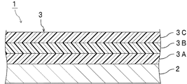
図2は、本発明の一実施形態に係る硬化物膜の製造方法により得られる硬化物膜を備える電子部品を示す断面図である。 FIG. 2: is sectional drawing which shows an electronic component provided with the hardened | cured material film obtained by the manufacturing method of the hardened | cured material film which concerns on one Embodiment of this invention.
図2に示す電子部品1は、電子部品本体2(第1の電子部品本体)と、電子部品本体2の表面上に配置された多層の硬化物膜3とを備える。多層の硬化物膜3は、複数の硬化物膜3A,3B,3Cを有する。多層の硬化物膜3では、複数の硬化物膜3A,3B,3Cが積層されている。多層の硬化物膜3は加熱後の硬化物膜である。多層の硬化物膜3の第1の電子部品本体2側とは反対の表面上に、第2の電子部品本体が配置されていてもよい。
An
上記電子部品本体としては、具体的には、半導体チップ、ダイシング後の半導体ウェーハ(分割された半導体ウェーハ)、コンデンサ、ダイオード、プリント基板、フレキシブルプリント基板、ガラスエポキシ基板及びガラス基板等が挙げられる。上記電子部品本体は、表面に硬化物膜を有していてもよい。硬化物膜を有する電子部品本体において、硬化物膜上に、硬化物膜を形成してもよい。 Specific examples of the electronic component body include semiconductor chips, semiconductor wafers after dicing (divided semiconductor wafers), capacitors, diodes, printed boards, flexible printed boards, glass epoxy boards, and glass boards. The electronic component body may have a cured product film on the surface. In the electronic component main body having a cured product film, a cured product film may be formed on the cured product film.
以下の本発明の一実施形態に係る硬化物膜の製造方法について説明する。 The manufacturing method of the hardened | cured material film | membrane which concerns on one embodiment of the following this invention is demonstrated.
先ず、図1(a)に示すように、電子部品本体2上に、インクジェット装置11を用いて、光硬化性及び熱硬化性を有しかつ液状である硬化性組成物12を塗布する(塗布工程)。ここでは、電子部品本体2の表面上に、全体に、硬化性組成物12を塗布している。塗布後、硬化性組成物12の液滴が互いに混ざり合い、図1(b)に示す状態になる。
First, as shown to Fig.1 (a), the
図3に示すように、インクジェット装置11は内部に、インクタンク21と、吐出部22と、循環流路部23とを有する。
As shown in FIG. 3, the ink jet device 11 includes an
循環流路部23は、循環流路部23内に、バッファタンク23Aとポンプ23Bとを有する。但し、図4に示すインクジェット装置11Xのように、循環流路部23Xは、循環流路部23X内に、バッファタンクとポンプとを有していなくてもよい。上記循環流路部は、上記循環流路部内に、上記バッファタンクを有することが好ましく、上記ポンプを有することが好ましい。また、上記循環流路部は、上記循環流路部内に、バッファタンク及びポンプの他に、流速計、温度計、フィルター等を有していてもよい。
The
インクタンク21には、上記硬化性組成物が貯留されている。吐出部22(インクジェットヘッド)から、上記硬化性組成物が吐出される。吐出部22は吐出ノズルを含む。インクタンク21に、吐出部22が接続されている。インクタンク21と吐出部22とは流路を介して接続されている。循環流路部23の一端は吐出部22に接続されており、他端はインクタンク21に接続されている。循環流路部23の内部を、上記硬化性組成物が流れる。
The
バッファタンク23A又はポンプ23Bが備えられる場合には、バッファタンク23A及びポンプ23Bはそれぞれ、吐出部22とインクタンク21との間に配置されることが好ましい。バッファタンク23Aはポンプ23Bよりも吐出部22側に配置されている。ポンプ23Bは、バッファタンク23Aよりもインクタンク21側に配置されている。バッファタンク23Aには、上記硬化性組成物が仮貯留される。
When the buffer tank 23A or the pump 23B is provided, the buffer tank 23A and the pump 23B are preferably disposed between the
上記吐出部としては、サーマル方式、バブル噴射方式、電磁バルブ方式又はピエゾ方式のインクジェットヘッド等が挙げられる。また、上記吐出部内の循環流路部としては、共通循環流路(マニフォールド)から塗出ノズルへ分岐しているエンドシュータータイプや塗出ノズルをインクが循環するサイドシュータータイプが挙げられる。硬化性組成物の吐出性を高めて、微細な硬化物膜の形成精度をより一層高める観点からは、上記インクジェット装置がピエゾ方式のインクジェットヘッドを用いるインクジェット装置であり、上記塗布工程において、ピエゾ素子の作用によって、上記硬化性組成物を塗布することが好ましい。 Examples of the ejection unit include a thermal type, bubble jet type, electromagnetic valve type, or piezoelectric type inkjet head. Further, examples of the circulation flow path section in the discharge section include an end shooter type branching from a common circulation flow path (manifold) to the coating nozzle and a side shooter type in which ink circulates through the coating nozzle. From the viewpoint of further improving the discharge accuracy of the curable composition and further improving the formation accuracy of the fine cured product film, the inkjet device is an inkjet device using a piezoelectric inkjet head, and in the coating step, a piezoelectric element is used. It is preferable to apply the curable composition by the action of the above.
上記硬化性組成物の循環方法に関しては、インクの自重を利用したり、ポンプ等を利用して加圧、減圧等を行い循環したりすることが可能である。これらは複数組み合わせて用いてもよい。ポンプとしてはシリンダ方式の無脈動ポンプ、プロペラポンプ、ギヤポンプ及びダイヤフラムポンプ等が挙げられる。循環効率を高めて、微細な硬化物膜の形成精度をより一層高める観点からは、上記循環流路部は、上記循環流路部内に上記硬化性組成物を移送させるポンプを含むことが好ましい。 Regarding the method for circulating the curable composition, it is possible to circulate by utilizing the weight of the ink or by applying pressure, depressurization or the like using a pump or the like. A plurality of these may be used in combination. Examples of the pump include a cylinder-type non-pulsation pump, a propeller pump, a gear pump, and a diaphragm pump. From the viewpoint of increasing the circulation efficiency and further improving the formation accuracy of the fine cured product film, the circulation channel part preferably includes a pump for transferring the curable composition into the circulation channel part.
上記吐出部の塗出ノズルにおいては、適切な圧力に保ちかつ、その範囲内で圧力変動(脈動)が少ないことが好ましい。ポンプ等を使用する場合にはポンプの脈動を抑えるためにポンプと上記吐出部との間に減衰器を設けることが好ましい。このような減衰器としては上記硬化性組成物が仮貯留されるバッファタンクや膜式のダンパ等が挙げられる。 In the coating nozzle of the discharge unit, it is preferable that the pressure is kept at an appropriate pressure and that the pressure fluctuation (pulsation) is small within the range. When a pump or the like is used, it is preferable to provide an attenuator between the pump and the discharge unit in order to suppress pump pulsation. Examples of such an attenuator include a buffer tank in which the curable composition is temporarily stored and a membrane damper.
厚みが厚い硬化物膜の形成精度をより一層高める観点からは、上記循環流路部は、上記循環流路部内に、上記硬化性組成物が仮貯留されるバッファタンクを含むことが好ましい。 From the viewpoint of further increasing the formation accuracy of the cured product film having a large thickness, the circulation channel part preferably includes a buffer tank in which the curable composition is temporarily stored in the circulation channel part.
上記の塗布工程において、インクジェット装置11内で、上記硬化性組成物をインクタンク21から吐出部22に移動させた後に、吐出部22から吐出されなかった上記硬化性組成物を、循環流路部23内を流してインクタンク21に移動させる。それによって、上記の塗布工程において、上記硬化性組成物を循環させながら、塗布する。
In the application step, after the curable composition is moved from the
次に、図1(b),(c)に示すように、上記の塗布工程後に、第1の光照射部13から塗布後の硬化性組成物12に光を照射して、硬化性組成物12の硬化を進行させる(第1の光照射工程)。それによって、第1の光照射部13により光が照射された予備硬化物膜12Aが形成される。後述する第2の光照射部14から光が照射される場合、第1の光照射部13から照射される光の波長や照射強度と、後述する第2の光照射部14から照射される光の波長や照射強度とが同じでも異なっていてもよい。硬化物膜における硬化性をより一層高める観点からは、第2の光照射部14から照射される光の照射強度が、第1の光照射部13から照射される光の照射強度より強い方が好ましい。光硬化性化合物と、光及び熱硬化性化合物とを用いる場合に、光硬化性を制御するために、上記第1の光照射工程と、後述する第2の光照射工程とを行うことが好ましい。
Next, as shown in FIGS. 1B and 1C, after the coating step, the
なお、「第1の光照射部13から塗布後の硬化性組成物12に光を照射して、硬化性組成物12の硬化を進行させる」には、反応を進行させて増粘状態にすることも含まれる。
In addition, in order to “light the
光照射を行う装置としては特に限定されず、紫外線を発生する発光ダイオード(UV−LED)、メタルハライドランプ、高圧水銀ランプ、及び超高圧水銀ランプ等が挙げられる。硬化物膜の形成精度をより一層高める観点からは、特に第1の光照射部に、UV−LEDを用いることが好ましい。 The device that performs light irradiation is not particularly limited, and examples thereof include a light emitting diode (UV-LED) that generates ultraviolet rays, a metal halide lamp, a high pressure mercury lamp, and an ultrahigh pressure mercury lamp. From the viewpoint of further improving the accuracy of forming the cured film, it is particularly preferable to use a UV-LED for the first light irradiation section.
次に、図1(c),(d)に示すように、上記の第1の光照射工程後の予備硬化物膜12A上にて、上記の塗布工程と上記の第1の光照射工程とを行い、予備硬化物膜12A上に他の予備硬化物膜12B,12Cを形成することにより、多層の予備硬化物膜12Xを形成する(多層化工程)。多層の予備硬化物膜12Xは、予備硬化物膜12A,12B,12Cを含む。上記の塗布工程と上記の第1の光照射工程とを複数回行い、積層数を増やす。
Next, as shown in FIGS. 1C and 1D, on the preliminary-cured material film 12A after the first light irradiation step, the coating step and the first light irradiation step are performed. And forming the other preliminary-cured
次に、図1(d),(e)に示すように、上記の多層化工程後に、第1の光照射部13とは別の第2の光照射部14から、多層の予備硬化物膜12X(予備硬化物膜12A,12B,12C)に光を照射して、多層の予備硬化物膜12Xの硬化をさらに進行させる(第2の光照射工程)。それによって、第2の光照射部14により光が照射された予備硬化物膜12Yが形成される。
Next, as shown in FIGS. 1D and 1E, after the multi-layering step, a multi-layer precured material film is formed from the second
上記の第2の光照射工程は、後述する加熱工程前に行われることが好ましい。厚みが厚い硬化物膜の形成精度をより一層高める観点からは、上記第2の光照射工程が行われることが好ましい。但し、上記第2の光照射工程は必ずしも行われる必要はなく、上記多層化工程後に、上記第2の光照射工程を行わずに、後述する加熱工程が行われてもよい。 The second light irradiation step is preferably performed before the heating step described later. From the viewpoint of further increasing the formation accuracy of the thick cured film, it is preferable that the second light irradiation step is performed. However, the second light irradiation step is not necessarily performed, and a heating step described later may be performed after the multilayering step without performing the second light irradiation step.
次に、上記多層化工程後かつ上記第2の光照射工程後に、予備硬化物膜12Yを加熱して、第2の光照射部14により光が照射された予備硬化物膜12Yを硬化させて、硬化物膜3を形成する(加熱工程)。なお、上記多層化工程後に、上記第2の光照射工程を行わない場合には、上記多層化工程後に、多層の予備硬化物膜12Xを加熱して、多層の予備硬化物膜12Xを硬化させて、硬化物膜を形成することができる(加熱工程)。このようにして、図2に示す電子部品1を得ることができる。
Next, after the multilayering step and the second light irradiation step, the preliminary-cured
上記の硬化物膜の製造方法において、硬化性組成物の吐出性及び移送性を高めて、厚みが厚い硬化物膜の形成精度をより一層高める観点からは、循環されている上記硬化性組成物の温度は好ましくは30℃以上、より好ましくは40℃以上、好ましくは120℃以下、より好ましくは100℃以下である。 In the manufacturing method of said hardened | cured material film, the said curable composition currently circulated from a viewpoint which raises the discharge property and transportability of a curable composition, and raises the formation precision of a hardened | cured material film with thick thickness further. The temperature is preferably 30 ° C. or higher, more preferably 40 ° C. or higher, preferably 120 ° C. or lower, more preferably 100 ° C. or lower.
硬化性組成物の吐出性を高めて、厚みが厚い硬化物膜の形成精度をより一層高める観点からは、上記硬化性組成物の吐出時の粘度は好ましくは3mPa・s以上、より好ましくは5mPa・s以上、好ましくは1500mPa・s以下、より好ましくは1200mPa・s以下である。 From the viewpoint of increasing the dischargeability of the curable composition and further increasing the accuracy of forming a thick cured film, the viscosity at the time of discharging the curable composition is preferably 3 mPa · s or more, more preferably 5 mPa. S or more, preferably 1500 mPa · s or less, more preferably 1200 mPa · s or less.
上記粘度は、JIS K2283に準拠して、E型粘度計(東機産業社製「TVE22L」)を用いて、吐出時の温度で測定される。 The viscosity is measured at an ejection temperature using an E-type viscometer (“TVE22L” manufactured by Toki Sangyo Co., Ltd.) in accordance with JIS K2283.
上記硬化性組成物は、光硬化性及び熱硬化性を有する。上記硬化性組成物は、光硬化性成分と熱硬化性成分とを含む。上記硬化性組成物は、光硬化性化合物(光の照射により硬化可能な硬化性化合物)と、熱硬化性化合物(加熱により硬化可能な硬化性化合物)と、光重合開始剤と、熱硬化剤とを含むことが好ましい。上記硬化性組成物は、光硬化性化合物と、光及び熱硬化性化合物(光の照射及び加熱の双方により硬化可能な硬化性化合物)と、熱硬化性化合物と、光重合開始剤と、熱硬化剤とを含むことが好ましい。上記硬化性組成物は、硬化促進剤を含むことが好ましい。 The said curable composition has photocurability and thermosetting. The said curable composition contains a photocurable component and a thermosetting component. The curable composition includes a photocurable compound (a curable compound that can be cured by light irradiation), a thermosetting compound (a curable compound that can be cured by heating), a photopolymerization initiator, and a thermosetting agent. Are preferably included. The curable composition comprises a photocurable compound, a light and thermosetting compound (a curable compound that can be cured by both light irradiation and heating), a thermosetting compound, a photopolymerization initiator, and heat. It preferably contains a curing agent. It is preferable that the said curable composition contains a hardening accelerator.
以下、上記硬化性組成物に含まれる各成分の詳細を説明する。 Hereinafter, the detail of each component contained in the said curable composition is demonstrated.
(硬化性化合物)
(光硬化性化合物)
上記光硬化性化合物としては、(メタ)アクリロイル基を有する硬化性化合物、ビニル基を有する硬化性化合物及びマレイミド基を有する硬化性化合物等が挙げられる。厚みが厚い硬化物膜の形成精度をより一層高める観点からは、上記光硬化性化合物は、(メタ)アクリロイル基(1個以上)を有することが好ましい。上記光硬化性化合物は、1種のみが用いられてもよく、2種以上が併用されてもよい。
(Curable compound)
(Photocurable compound)
Examples of the photocurable compound include a curable compound having a (meth) acryloyl group, a curable compound having a vinyl group, and a curable compound having a maleimide group. From the viewpoint of further improving the formation accuracy of the cured film having a large thickness, the photocurable compound preferably has a (meth) acryloyl group (one or more). As for the said photocurable compound, only 1 type may be used and 2 or more types may be used together.
本明細書では、上記(メタ)アクリロイル基を有する硬化性化合物は、メタクリロイル基及びアクリロイル基の内の少なくとも一方を有する化合物を意味する。 In the present specification, the curable compound having the (meth) acryloyl group means a compound having at least one of a methacryloyl group and an acryloyl group.
上記光硬化性化合物として、光反応性基を2個以上有する多官能化合物(A1)を用いてもよく、光反応性基を1個有する単官能化合物(A2)を用いてもよい。 As the photocurable compound, a polyfunctional compound (A1) having two or more photoreactive groups may be used, or a monofunctional compound (A2) having one photoreactive group may be used.
厚みが厚い硬化物膜の形成精度をより一層高める観点からは、上記硬化性組成物が、上記光硬化性化合物として、(メタ)アクリロイル基を1個有する単官能化合物(A2)と、(メタ)アクリロイル基を2個以上有する多官能化合物(A1)とを含むことが好ましい。 From the viewpoint of further increasing the formation accuracy of a cured product film having a large thickness, the curable composition has, as the photocurable compound, a monofunctional compound (A2) having one (meth) acryloyl group, And a polyfunctional compound (A1) having two or more acryloyl groups.
上記多官能化合物(A1)としては、多価アルコールの(メタ)アクリル酸付加物、多価アルコールのアルキレンオキサイド変性物の(メタ)アクリル酸付加物、ウレタン(メタ)アクリレート類、及びポリエステル(メタ)アクリレート類等が挙げられる。上記多価アルコールとしては、ジエチレングリコール、トリエチレングリコール、ポリエチレングリコール、ジプロピレングリコール、トリプロピレングリコール、ポリプロピレングリコール、トリメチロールプロパン、シクロヘキサンジメタノール、トリシクロデカンジメタノール、ビスフェノールAのアルキレンオキシド付加物、及びペンタエリスリトール等が挙げられる。 Examples of the polyfunctional compound (A1) include (meth) acrylic acid adducts of polyhydric alcohols, (meth) acrylic acid adducts of alkylene oxide modified products of polyhydric alcohols, urethane (meth) acrylates, and polyesters (meta ) Acrylates and the like. Examples of the polyhydric alcohol include diethylene glycol, triethylene glycol, polyethylene glycol, dipropylene glycol, tripropylene glycol, polypropylene glycol, trimethylol propane, cyclohexane dimethanol, tricyclodecane dimethanol, an alkylene oxide adduct of bisphenol A, and Examples include pentaerythritol.
上記多官能化合物(A1)の具体例としては、トリシクロデカンジメタノールジ(メタ)アクリレート、イソボルニルジメタノールジ(メタ)アクリレート及びジシクロペンテニルジメタノールジ(メタ)アクリレート等が挙げられる。なかでも、硬化物の耐湿熱性をより一層高める観点からは、上記多官能化合物(A1)は、トリシクロデカンジメタノールジ(メタ)アクリレートであることが好ましい。上記「(メタ)アクリレート」の用語は、アクリレートとメタクリレートとを示す。 Specific examples of the polyfunctional compound (A1) include tricyclodecane dimethanol di (meth) acrylate, isobornyl dimethanol di (meth) acrylate, dicyclopentenyl dimethanol di (meth) acrylate, and the like. Especially, it is preferable that the said polyfunctional compound (A1) is tricyclodecane dimethanol di (meth) acrylate from a viewpoint of improving the heat-and-moisture resistance of hardened | cured material further. The term “(meth) acrylate” refers to acrylate and methacrylate.
上記「(メタ)アクリレート」の用語は、アクリレート又はメタクリレートを示す。上記「(メタ)アクリル」の用語は、アクリル又はメタクリルを示す。 The term “(meth) acrylate” refers to acrylate or methacrylate. The term “(meth) acryl” refers to acryl or methacryl.
上記多官能化合物(A1)は、多環骨格を有し、かつ(メタ)アクリロイル基を2個以上有する多官能化合物(A1)であることが好ましい。多官能化合物(A1)の使用により、上記硬化性組成物の硬化物の耐湿熱性を高くすることができる。従って、電子部品の信頼性を高めることができる。 The polyfunctional compound (A1) is preferably a polyfunctional compound (A1) having a polycyclic skeleton and having two or more (meth) acryloyl groups. The use of the polyfunctional compound (A1) can increase the heat and moisture resistance of the cured product of the curable composition. Therefore, the reliability of the electronic component can be increased.
上記多官能化合物(A1)は、多環骨格を有し、かつ(メタ)アクリロイル基を2個以上有すれば特に限定されない。多官能化合物(A1)として、多環骨格を有し、かつ(メタ)アクリロイル基を2個以上有する従来公知の多官能化合物を用いることができる。上記多官能化合物(A1)は、(メタ)アクリロイル基を2個以上有するため、光の照射により重合が進行し、硬化する。上記多官能化合物(A1)は、1種のみが用いられてもよく、2種以上が併用されてもよい。 The polyfunctional compound (A1) is not particularly limited as long as it has a polycyclic skeleton and two or more (meth) acryloyl groups. As the polyfunctional compound (A1), a conventionally known polyfunctional compound having a polycyclic skeleton and having two or more (meth) acryloyl groups can be used. Since the polyfunctional compound (A1) has two or more (meth) acryloyl groups, the polymerization proceeds and is cured by light irradiation. As for the said polyfunctional compound (A1), only 1 type may be used and 2 or more types may be used together.
上記多官能化合物(A1)の具体例としては、トリシクロデカンジメタノールジ(メタ)アクリレート、イソボルニルジメタノールジ(メタ)アクリレート及びジシクロペンテニルジメタノールジ(メタ)アクリレート等が挙げられる。なかでも、硬化物の耐湿熱性をより一層高める観点からは、上記多官能化合物(A1)は、トリシクロデカンジメタノールジ(メタ)アクリレートであることが好ましい。 Specific examples of the polyfunctional compound (A1) include tricyclodecane dimethanol di (meth) acrylate, isobornyl dimethanol di (meth) acrylate, dicyclopentenyl dimethanol di (meth) acrylate, and the like. Especially, it is preferable that the said polyfunctional compound (A1) is tricyclodecane dimethanol di (meth) acrylate from a viewpoint of improving the heat-and-moisture resistance of hardened | cured material further.
上記多官能化合物(A1)及び後述する単官能化合物(A2)における上記「多環骨格」とは、複数の環状骨格を連続して有する構造を示す。多官能化合物(A1)及び単官能化合物(A2)における上記多環骨格としてはそれぞれ、多環脂環式骨格及び多環芳香族骨格等が挙げられる。 The “polycyclic skeleton” in the polyfunctional compound (A1) and the monofunctional compound (A2) described later indicates a structure having a plurality of cyclic skeletons continuously. Examples of the polycyclic skeleton in the polyfunctional compound (A1) and the monofunctional compound (A2) include a polycyclic alicyclic skeleton and a polycyclic aromatic skeleton.
上記多環脂環式骨格としては、ビシクロアルカン骨格、トリシクロアルカン骨格、テトラシクロアルカン骨格及びイソボルニル骨格等が挙げられる。 Examples of the polycyclic alicyclic skeleton include a bicycloalkane skeleton, a tricycloalkane skeleton, a tetracycloalkane skeleton, and an isobornyl skeleton.
上記多環芳香族骨格としては、ナフタレン環骨格、アントラセン環骨格、フェナントレン環骨格、テトラセン環骨格、クリセン環骨格、トリフェニレン環骨格、テトラフェン環骨格、ピレン環骨格、ペンタセン環骨格、ピセン環骨格及びペリレン環骨格等が挙げられる。 Examples of the polycyclic aromatic skeleton include naphthalene ring skeleton, anthracene ring skeleton, phenanthrene ring skeleton, tetracene ring skeleton, chrysene ring skeleton, triphenylene ring skeleton, tetraphen ring skeleton, pyrene ring skeleton, pentacene ring skeleton, picene ring skeleton and Examples include perylene ring skeletons.
上記単官能化合物(A2)の具体例としては、イソボルニル(メタ)アクリレート、ジヒドロキシシクロペンタジエニル(メタ)アクリレート、ジシクロペンテニル(メタ)アクリレート、ジシクロペンテニルオキシエチル(メタ)アクリレート、ジシクロペンタニル(メタ)アクリレート及びナフチル(メタ)アクリレート等が挙げられる。なかでも、硬化物の耐湿熱性をより一層高める観点からは、上記単官能化合物(A2)は、イソボルニル(メタ)アクリレート、ジヒドロキシシクロペンタジエニル(メタ)アクリレート、ジシクロペンテニル(メタ)アクリレート、ジシクロペンテニルオキシエチル(メタ)アクリレート及びジシクロペンタニル(メタ)アクリレートからなる群から選択された少なくとも1種であることが好ましい。 Specific examples of the monofunctional compound (A2) include isobornyl (meth) acrylate, dihydroxycyclopentadienyl (meth) acrylate, dicyclopentenyl (meth) acrylate, dicyclopentenyloxyethyl (meth) acrylate, dicyclopenta Examples include nyl (meth) acrylate and naphthyl (meth) acrylate. Among these, from the viewpoint of further improving the heat and heat resistance of the cured product, the monofunctional compound (A2) is composed of isobornyl (meth) acrylate, dihydroxycyclopentadienyl (meth) acrylate, dicyclopentenyl (meth) acrylate, di It is preferably at least one selected from the group consisting of cyclopentenyloxyethyl (meth) acrylate and dicyclopentanyl (meth) acrylate.
上記ビニル基を有する化合物としてはビニルエーテル類、エチレン誘導体、スチレン、クロロメチルスチレン、α−メチルスチレン、無水マレイン酸、ジシクロペンタジエン、N−ビニルピロリドン及びN−ビニルホルムアミド等が挙げられる。 Examples of the compound having a vinyl group include vinyl ethers, ethylene derivatives, styrene, chloromethyl styrene, α-methyl styrene, maleic anhydride, dicyclopentadiene, N-vinyl pyrrolidone, and N-vinyl formamide.
上記マレイミド基を有する化合物としては特に限定されず、例えば、N−メチルマレイミド、N−エチルマレイミド、N−ヘキシルマレイミド、N−プロピルマレイミド、N−ブチルマレイミド、N−オクチルマレイミド、N−ドデシルマレイミド、N−シクロヘキシルマレイミド、N−フェニルマレイミド、N−p−カルボキシフェニルマレイミド、N−p−ヒドロキシフェニルマレイミド、N−p−クロロフェニルマレイミド、N−p−トリルマレイミド、N−p−キシリルマレイミド、N−o−クロロフェニルマレイミド、N−o−トリルマレイミド、N−ベンジルマレイミド、N−2,5−ジエチルフェニルマレイミド、N−2,5−ジメチルフェニルマレイミド、N−m−トリルマレイミド、N−α−ナフチルマレイミド、N−o−キシリルマレイミド、N−m−キシリルマレイミド、ビスマレイミドメタン、1,2−ビスマレイミドエタン、1,6−ビスマレイミドヘキサン、ビスマレイミドドデカン、N,N’−m−フェニレンジマレイミド、N,N’−p−フェニレンジマレイミド、4,4’−ビスマレイミドジフェニルエーテル、4,4’−ビスマレイミドジフェニルメタン、4,4’−ビスマレイミド−ジ(3−メチルフェニル)メタン、4,4’−ビスマレイミド−ジ(3−エチルフェニル)メタン、4,4’−ビスマレイミド−ジ(3−メチル−5−エチル−フェニル)メタン、N,N’−(2,2−ビス−(4−フェノキシフェニル)プロパン)ジマレイミド、N,N’−2,4−トリレンジマレイミド、N,N’−2,6−トリレンジマレイミド、及びN,N’−m−キシリレンジマレイミド等が挙げられる。 The compound having a maleimide group is not particularly limited. For example, N-methylmaleimide, N-ethylmaleimide, N-hexylmaleimide, N-propylmaleimide, N-butylmaleimide, N-octylmaleimide, N-dodecylmaleimide, N-cyclohexylmaleimide, N-phenylmaleimide, Np-carboxyphenylmaleimide, Np-hydroxyphenylmaleimide, Np-chlorophenylmaleimide, Np-tolylmaleimide, Np-xylylmaleimide, N- o-chlorophenylmaleimide, N-o-tolylmaleimide, N-benzylmaleimide, N-2,5-diethylphenylmaleimide, N-2,5-dimethylphenylmaleimide, Nm-tolylmaleimide, N-α-naphthylmaleimide , N-o Xylylmaleimide, Nm-xylylmaleimide, bismaleimide methane, 1,2-bismaleimide ethane, 1,6-bismaleimide hexane, bismaleimide dodecane, N, N′-m-phenylenedimaleimide, N, N '-P-phenylenedimaleimide, 4,4'-bismaleimide diphenyl ether, 4,4'-bismaleimide diphenylmethane, 4,4'-bismaleimide-di (3-methylphenyl) methane, 4,4'-bismaleimide -Di (3-ethylphenyl) methane, 4,4'-bismaleimide-di (3-methyl-5-ethyl-phenyl) methane, N, N '-(2,2-bis- (4-phenoxyphenyl) Propane) dimaleimide, N, N'-2,4-tolylene dialeimide, N, N'-2,6-tolylene dialeimide, and N, N'-m-xylylene dimaleimide and the like can be mentioned.
絶縁信頼性や接着信頼性をより一層高める観点から、上記光硬化性化合物は、ジシクロペンタジエン骨格を有することが好ましい。 From the viewpoint of further increasing the insulation reliability and adhesion reliability, the photocurable compound preferably has a dicyclopentadiene skeleton.
厚みが厚い硬化物膜の形成精度をより一層高める観点からは、上記硬化性組成物100重量%中、上記光硬化性化合物の含有量は、好ましくは40重量%以上、より好ましくは50重量%以上、好ましくは90重量%以下、より好ましくは85重量%以下である。 From the viewpoint of further increasing the accuracy of forming a cured film having a large thickness, the content of the photocurable compound is preferably 40% by weight or more, more preferably 50% by weight in 100% by weight of the curable composition. As mentioned above, Preferably it is 90 weight% or less, More preferably, it is 85 weight% or less.
(光及び熱硬化性化合物)
上記光及び熱硬化性化合物としては、各種の光硬化性官能基と各種の熱硬化性官能基とを有する化合物が挙げられる。厚みが厚い硬化物膜の形成精度をより一層高める観点からは、上記光及び熱硬化性化合物は、(メタ)アクリロイル基と環状エーテル基とを有することが好ましく、(メタ)アクリロイル基とエポキシ基とを有することが好ましい。上記光及び熱硬化性化合物は、1種のみが用いられてもよく、2種以上が併用されてもよい。
(Light and thermosetting compounds)
Examples of the light and thermosetting compounds include compounds having various photocurable functional groups and various thermosetting functional groups. From the viewpoint of further increasing the formation accuracy of a cured film having a large thickness, the light and thermosetting compound preferably has a (meth) acryloyl group and a cyclic ether group, and a (meth) acryloyl group and an epoxy group. It is preferable to have. As for the said light and a thermosetting compound, only 1 type may be used and 2 or more types may be used together.
上記光及び熱硬化性化合物としては、特に限定されないが、(メタ)アクリロイル基とエポキシ基を有する化合物、エポキシ化合物の部分(メタ)アクリル化物、及びウレタン変性(メタ)アクリルエポキシ化合物等が挙げられる。 Although it does not specifically limit as said light and a thermosetting compound, The compound which has a (meth) acryloyl group and an epoxy group, the partial (meth) acrylate of an epoxy compound, a urethane modified (meth) acryl epoxy compound, etc. are mentioned. .
上記(メタ)アクリロイル基とエポキシ基を有する化合物としては、グリシジル(メタ)アクリレート、及び4−ヒドロキシブチル(メタ)アクリレートグリシジルエーテル等が挙げられる。 Examples of the compound having the (meth) acryloyl group and the epoxy group include glycidyl (meth) acrylate and 4-hydroxybutyl (meth) acrylate glycidyl ether.
上記エポキシ化合物の部分(メタ)アクリル化物としては、エポキシ化合物と(メタ)アクリル酸とを、常法に従って触媒の存在下で反応させることにより得られる。上記エポキシ化合物の部分(メタ)アクリル化物に用いることができるエポキシ化合物としては、ノボラック型エポキシ化合物及びビスフェノール型エポキシ化合物等が挙げられる。上記ノボラック型エポキシ化合物としては、フェノールノボラック型エポキシ化合物、クレゾールノボラック型エポキシ化合物、ビフェニルノボラック型エポキシ化合物、トリスフェノールノボラック型エポキシ化合物、及びジシクロペンタジエンノボラック型エポキシ化合物等が挙げられる。上記ビスフェノール型エポキシ化合物としては、ビスフェノールA型エポキシ化合物、ビスフェノールF型エポキシ化合物、2,2’−ジアリルビスフェノールA型エポキシ化合物、水添ビスフェノール型エポキシ化合物、及びポリオキシプロピレンビスフェノールA型エポキシ化合物等が挙げられる。エポキシ化合物と(メタ)アクリル酸との配合量を適宜変更することにより、所望のアクリル化率のエポキシ化合物を得ることが可能である。エポキシ基1当量に対してカルボン酸の配合量は、好ましくは0.1当量以上、より好ましくは0.2当量以上、好ましくは0.7当量以下、より好ましくは0.5当量以下である。 The partial (meth) acrylated product of the epoxy compound can be obtained by reacting an epoxy compound and (meth) acrylic acid in the presence of a catalyst according to a conventional method. Examples of the epoxy compound that can be used for the partial (meth) acrylate of the epoxy compound include novolac-type epoxy compounds and bisphenol-type epoxy compounds. Examples of the novolak type epoxy compound include a phenol novolak type epoxy compound, a cresol novolak type epoxy compound, a biphenyl novolak type epoxy compound, a trisphenol novolak type epoxy compound, a dicyclopentadiene novolak type epoxy compound, and the like. Examples of the bisphenol type epoxy compound include a bisphenol A type epoxy compound, a bisphenol F type epoxy compound, a 2,2′-diallyl bisphenol A type epoxy compound, a hydrogenated bisphenol type epoxy compound, and a polyoxypropylene bisphenol A type epoxy compound. Can be mentioned. By appropriately changing the blending amount of the epoxy compound and (meth) acrylic acid, an epoxy compound having a desired acrylate ratio can be obtained. The blending amount of the carboxylic acid with respect to 1 equivalent of epoxy group is preferably 0.1 equivalent or more, more preferably 0.2 equivalent or more, preferably 0.7 equivalent or less, more preferably 0.5 equivalent or less.
上記ウレタン変性(メタ)アクリルエポキシ化合物は、例えば、以下の方法によって得られる。ポリオールと2官能以上のイソシアネートを反応させ、さらに残りのイソシアネート基に、酸基を有する(メタ)アクリルモノマー及びグリシドールを反応させる。または、ポリオールを用いず、2官能以上のイソシアネートに水酸基を有する(メタ)アクリルモノマーとグリシドールとを反応させてもよい。または、イソシアネート基を有する(メタ)アクリレートモノマーにグリシドールを反応させても、上記ウレタン変性(メタ)アクリルエポキシ化合物が得られる。具体的には、例えば、まず、トリメチロールプロパン1モルとイソホロンジイソシアネート3モルとを錫系触媒下で反応させる。得られた化合物中に残るイソシアネート基と、水酸基を有するアクリルモノマーであるヒドロキシエチルアクリレート、及び水酸基を有するエポキシであるグリシドールを反応させることにより、上記ウレタン変性(メタ)アクリルエポキシ化合物が得られる。 The urethane-modified (meth) acryl epoxy compound is obtained, for example, by the following method. A polyol and a bifunctional or higher functional isocyanate are reacted, and the remaining isocyanate group is reacted with a (meth) acryl monomer having an acid group and glycidol. Alternatively, a (meth) acryl monomer having a hydroxyl group in a bifunctional or higher isocyanate and glycidol may be reacted without using a polyol. Alternatively, the urethane-modified (meth) acryl epoxy compound can be obtained by reacting glycidol with a (meth) acrylate monomer having an isocyanate group. Specifically, for example, first, 1 mol of trimethylolpropane and 3 mol of isophorone diisocyanate are reacted under a tin-based catalyst. The urethane-modified (meth) acrylic epoxy compound is obtained by reacting the isocyanate group remaining in the obtained compound with hydroxyethyl acrylate which is an acrylic monomer having a hydroxyl group and glycidol which is an epoxy having a hydroxyl group.
上記ポリオールとしては、特に限定されず、例えば、エチレングリコール、グリセリン、ソルビトール、トリメチロールプロパン、及び(ポリ)プロピレングリコール等が挙げられる。 The polyol is not particularly limited, and examples thereof include ethylene glycol, glycerin, sorbitol, trimethylolpropane, and (poly) propylene glycol.
上記イソシアネートは、2官能以上であれば、特に限定されない。上記イソシアネートとしては、例えば、イソホロンジイソシアネート、2,4−トリレンジイソシアネート、2,6−トリレンジイソシアネート、ヘキサメチレンジイソシアネート、トリメチルヘキサメチレンジイソシアネート、ジフェニルメタン−4,4’−ジイソシアネート(MDI)、水添MDI、ポリメリックMDI、1,5−ナフタレンジイソシアネート、ノルボルナンジイソシネート、トリジンジイソシアネート、キシリレンジイオシアネート(XDI)、水添XDI、リジンジイソシアネート、トリフェニルメタントリイソシアネート、トリス(イソシアネートフェニル)チオフォスフェート、テトラメチルキシレンジイソシアネート、及び1,6,10−ウンデカントリイソシアネート等が挙げられる。 The isocyanate is not particularly limited as long as it is bifunctional or higher. Examples of the isocyanate include isophorone diisocyanate, 2,4-tolylene diisocyanate, 2,6-tolylene diisocyanate, hexamethylene diisocyanate, trimethylhexamethylene diisocyanate, diphenylmethane-4,4′-diisocyanate (MDI), and hydrogenated MDI. , Polymeric MDI, 1,5-naphthalene diisocyanate, norbornane diisocyanate, tolidine diisocyanate, xylylene diisocyanate (XDI), hydrogenated XDI, lysine diisocyanate, triphenylmethane triisocyanate, tris (isocyanatophenyl) thiophosphate, tetramethyl Examples include xylene diisocyanate and 1,6,10-undecane triisocyanate.
厚みが厚い硬化物膜の形成精度をより一層高める観点からは、上記硬化性組成物100重量%中、上記光及び熱硬化性化合物の含有量は、好ましくは0.5重量%以上、より好ましくは1重量%以上、好ましくは60重量%以下、より好ましくは50重量%以下である。 From the viewpoint of further increasing the formation accuracy of the cured product film having a large thickness, the content of the light and thermosetting compound in the curable composition of 100% by weight is preferably 0.5% by weight or more, more preferably. Is 1% by weight or more, preferably 60% by weight or less, more preferably 50% by weight or less.
厚みが厚い硬化物膜の形成精度をより一層高める観点からは、上記硬化性組成物100重量%中、上記光硬化性化合物と上記光及び熱硬化性化合物との合計の含有量は、好ましくは40重量%以上、より好ましくは50重量%以上、好ましくは90重量%以下、より好ましくは85重量%以下である。 From the viewpoint of further increasing the formation accuracy of the cured film having a large thickness, the total content of the photocurable compound and the light and thermosetting compound in 100% by weight of the curable composition is preferably It is 40% by weight or more, more preferably 50% by weight or more, preferably 90% by weight or less, more preferably 85% by weight or less.
(熱硬化性化合物)
上記熱硬化性化合物としては、環状エーテル基を有する熱硬化性化合物、及びチイラン基を有する熱硬化性化合物等が挙げられる。厚みが厚い硬化物膜の形成精度をより一層高める観点からは、上記熱硬化性化合物は、環状エーテル基を有する熱硬化性化合物であることが好ましく、エポキシ基を有する熱硬化性化合物(エポキシ化合物)であることがより好ましい。上記熱硬化性化合物は、1種のみが用いられてもよく、2種以上が併用されてもよい。
(Thermosetting compound)
Examples of the thermosetting compound include a thermosetting compound having a cyclic ether group, a thermosetting compound having a thiirane group, and the like. From the viewpoint of further increasing the formation accuracy of the cured film having a large thickness, the thermosetting compound is preferably a thermosetting compound having a cyclic ether group, and a thermosetting compound having an epoxy group (epoxy compound). ) Is more preferable. As for the said thermosetting compound, only 1 type may be used and 2 or more types may be used together.
上記エポキシ化合物としては特に限定されず、例えば、ノボラック型エポキシ化合物及びビスフェノール型エポキシ化合物等が挙げられる。上記ノボラック型エポキシ化合物としては、フェノールノボラック型エポキシ化合物、クレゾールノボラック型エポキシ化合物、ビフェニルノボラック型エポキシ化合物、トリスフェノールノボラック型エポキシ化合物、及びジシクロペンタジエンノボラック型エポキシ化合物等が挙げられる。上記ビスフェノール型エポキシ化合物としては、ビスフェノールA型エポキシ化合物、ビスフェノールF型エポキシ化合物、2,2’−ジアリルビスフェノールA型エポキシ化合物、水添ビスフェノール型エポキシ化合物、及びポリオキシプロピレンビスフェノールA型エポキシ化合物等が挙げられる。また、上記エポキシ化合物としては、その他に、環式脂肪族エポキシ化合物、及びグリシジルアミン等も挙げられる。 The epoxy compound is not particularly limited, and examples thereof include novolak type epoxy compounds and bisphenol type epoxy compounds. Examples of the novolak type epoxy compound include a phenol novolak type epoxy compound, a cresol novolak type epoxy compound, a biphenyl novolak type epoxy compound, a trisphenol novolak type epoxy compound, a dicyclopentadiene novolak type epoxy compound, and the like. Examples of the bisphenol type epoxy compound include a bisphenol A type epoxy compound, a bisphenol F type epoxy compound, a 2,2′-diallyl bisphenol A type epoxy compound, a hydrogenated bisphenol type epoxy compound, and a polyoxypropylene bisphenol A type epoxy compound. Can be mentioned. In addition, examples of the epoxy compound include a cycloaliphatic epoxy compound and glycidylamine.
厚みが厚い硬化物膜の形成精度をより一層高める観点からは、上記硬化性組成物100重量%中、上記熱硬化性化合物の含有量は、好ましくは3重量%以上、より好ましくは5重量%以上、好ましくは60重量%以下、より好ましくは50重量%以下である。 From the viewpoint of further improving the accuracy of forming a cured film having a large thickness, the content of the thermosetting compound is preferably 3% by weight or more, more preferably 5% by weight in 100% by weight of the curable composition. As mentioned above, Preferably it is 60 weight% or less, More preferably, it is 50 weight% or less.
(光重合開始剤)
上記光重合開始剤としては、光ラジカル重合開始剤及び光カチオン重合開始剤等が挙げられる。上記光重合開始剤は、光ラジカル重合開始剤であることが好ましい。上記光重合開始剤は、1種のみが用いられてもよく、2種以上が併用されてもよい。
(Photopolymerization initiator)
Examples of the photopolymerization initiator include a photoradical polymerization initiator and a photocationic polymerization initiator. The photopolymerization initiator is preferably a photoradical polymerization initiator. As for the said photoinitiator, only 1 type may be used and 2 or more types may be used together.
上記光ラジカル重合開始剤は特に限定されない。上記光ラジカル重合開始剤は、光の照射によりラジカルを発生し、ラジカル重合反応を開始するための化合物である。上記光ラジカル重合開始剤の具体例としては、例えば、ベンゾイン、ベンゾインアルキルエーテル類、アセトフェノン類、アミノアセトフェノン類、アントラキノン類、チオキサントン類、ケタール類、2,4,5−トリアリールイミダゾール二量体、リボフラビンテトラブチレート、チオール化合物、2,4,6−トリス−s−トリアジン、有機ハロゲン化合物、ベンゾフェノン類、キサントン類及び2,4,6−トリメチルベンゾイルジフェニルホスフィンオキサイド等が挙げられる。上記光ラジカル重合開始剤は、1種のみが用いられてもよく、2種以上が併用されてもよい。 The photo radical polymerization initiator is not particularly limited. The photo radical polymerization initiator is a compound for generating radicals upon light irradiation and initiating a radical polymerization reaction. Specific examples of the photo radical polymerization initiator include, for example, benzoin, benzoin alkyl ethers, acetophenones, aminoacetophenones, anthraquinones, thioxanthones, ketals, 2,4,5-triarylimidazole dimers, Examples include riboflavin tetrabutyrate, thiol compounds, 2,4,6-tris-s-triazine, organic halogen compounds, benzophenones, xanthones, and 2,4,6-trimethylbenzoyldiphenylphosphine oxide. As for the said radical photopolymerization initiator, only 1 type may be used and 2 or more types may be used together.
上記光ラジカル重合開始剤とともに、光重合開始助剤を用いてもよい。該光重合開始助剤としては、N,N−ジメチルアミノ安息香酸エチルエステル、N,N−ジメチルアミノ安息香酸イソアミルエステル、ペンチル−4−ジメチルアミノベンゾエート、トリエチルアミン及びトリエタノールアミン等が挙げられる。これら以外の光重合開始助剤を用いてもよい。上記光重合開始助剤は、1種のみが用いられてもよく、2種以上が併用されてもよい。 A photopolymerization initiation assistant may be used together with the photo radical polymerization initiator. Examples of the photopolymerization initiation assistant include N, N-dimethylaminobenzoic acid ethyl ester, N, N-dimethylaminobenzoic acid isoamyl ester, pentyl-4-dimethylaminobenzoate, triethylamine, and triethanolamine. Photopolymerization initiation assistants other than these may be used. As for the said photoinitiation adjuvant, only 1 type may be used and 2 or more types may be used together.
また、可視光領域に吸収があるCGI−784等(チバ・スペシャルティ・ケミカルズ社製)のチタノセン化合物などを、光反応を促進するために用いてもよい。 In addition, a titanocene compound such as CGI-784 (manufactured by Ciba Specialty Chemicals) having absorption in the visible light region may be used to promote the photoreaction.
上記光カチオン重合開始剤としては特に限定されず、例えば、スルホニウム塩、ヨードニウム塩、メタロセン化合物及びベンゾイントシレート等が挙げられる。上記光カチオン重合開始剤は、1種のみが用いられてもよく、2種以上が併用されてもよい。 It does not specifically limit as said photocationic polymerization initiator, For example, a sulfonium salt, an iodonium salt, a metallocene compound, a benzoin tosylate etc. are mentioned. As for the said photocationic polymerization initiator, only 1 type may be used and 2 or more types may be used together.
上記硬化性組成物100重量%中、上記光重合開始剤の含有量は好ましくは0.1重量%以上、より好ましくは0.2重量%以上、好ましくは10重量%以下、より好ましくは5重量%以下である。 In 100% by weight of the curable composition, the content of the photopolymerization initiator is preferably 0.1% by weight or more, more preferably 0.2% by weight or more, preferably 10% by weight or less, more preferably 5% by weight. % Or less.
(熱硬化剤)
上記熱硬化剤としては、有機酸、アミン化合物、アミド化合物、ヒドラジド化合物、イミダゾール化合物、イミダゾリン化合物、フェノール化合物、ユリア化合物、ポリスルフィッド化合物及び酸無水物等が挙げられる。上記熱硬化剤として、アミン−エポキシアダクトなどの変性ポリアミン化合物を用いてもよい。これら以外の熱硬化剤を用いてもよい。上記熱硬化剤は、1種のみが用いられてもよく、2種以上が併用されてもよい。
(Thermosetting agent)
Examples of the thermosetting agent include organic acids, amine compounds, amide compounds, hydrazide compounds, imidazole compounds, imidazoline compounds, phenol compounds, urea compounds, polysulfide compounds, and acid anhydrides. A modified polyamine compound such as an amine-epoxy adduct may be used as the thermosetting agent. Thermosetting agents other than these may be used. As for the said thermosetting agent, only 1 type may be used and 2 or more types may be used together.
上記アミン化合物とは、1個以上の1〜3級のアミノ基を有する化合物を意味する。上記アミン化合物としては、例えば、(1)脂肪族ポリアミン、(2)脂環族ポリアミン、(3)芳香族ポリアミン、(4)ヒドラジド、及び(5)グアニジン誘導体等が挙げられる。また、エポキシ化合物付加ポリアミン(エポキシ化合物とポリアミンの反応物)、マイケル付加ポリアミン(α、β不飽和ケトンとポリアミンの反応物)、マンニッヒ付加ポリアミン(ポリアミンとホルマリン及びフェノールの縮合体)、チオ尿素付加ポリアミン(チオ尿素とポリアミンの反応物)、ケトン封鎖ポリアミン(ケトン化合物とポリアミンの反応物[ケチミン])などのアダクト体を用いてもよい。 The amine compound means a compound having one or more primary to tertiary amino groups. Examples of the amine compound include (1) aliphatic polyamines, (2) alicyclic polyamines, (3) aromatic polyamines, (4) hydrazides, and (5) guanidine derivatives. In addition, epoxy compound addition polyamine (reaction product of epoxy compound and polyamine), Michael addition polyamine (reaction product of α, β unsaturated ketone and polyamine), Mannich addition polyamine (condensate of polyamine, formalin and phenol), thiourea addition Adducts such as polyamine (reaction product of thiourea and polyamine) and ketone-capped polyamine (reaction product of ketone compound and polyamine [ketimine]) may also be used.
上記(1)脂肪族ポリアミンとしては、ジエチレントリアミン、トリエチレンテトラミン、テトラエチレンペンタミン、及びジエチルアミノプロピルアミン等が挙げられる。 Examples of the (1) aliphatic polyamine include diethylenetriamine, triethylenetetramine, tetraethylenepentamine, and diethylaminopropylamine.
上記(2)脂環族ポリアミンとしては、メンセンジアミン、イソホロンジアミン、N−アミノエチルピペラジン、3,9−ビス(3−アミノプロピル)−2,4,8,10−テトラオキサスピロ(5,5)ウンデカンアダクト、ビス(4−アミノ−3−メチルシクロヘキシル)メタン、及びビス(4−アミノシクロヘキシル)メタン等が挙げられる。 Examples of the (2) alicyclic polyamine include mensendiamine, isophoronediamine, N-aminoethylpiperazine, 3,9-bis (3-aminopropyl) -2,4,8,10-tetraoxaspiro (5, 5) Undecane adduct, bis (4-amino-3-methylcyclohexyl) methane, bis (4-aminocyclohexyl) methane and the like.
上記(3)芳香族ポリアミンとしては、m−フェニレンジアミン、p−フェニレンジアミン、o−キシレンジアミン、m−キシレンジアミン、p−キシレンジアミン、4,4−ジアミノジフェニルメタン、4,4−ジアミノジフェニルプロパン、4,4−ジアミノジフェニルスルフォン、4,4−ジアミノジシクロヘキサン、ビス(4−アミノフェニル)フェニルメタン、1,5−ジアミノナフタレン、1,1−ビス(4−アミノフェニル)シクロヘキサン、2,2−ビス[(4−アミノフェノキシ)フェニル]プロパン、ビス[4−(4−アミノフェノキシ)フェニル]スルフォン、1,3−ビス(4−アミノフェノキシ)ベンゼン、4,4−メチレン−ビス(2−クロロアニリン)、及び4,4−ジアミノジフェニルスルフォン等が挙げられる。 Examples of the aromatic polyamine (3) include m-phenylenediamine, p-phenylenediamine, o-xylenediamine, m-xylenediamine, p-xylenediamine, 4,4-diaminodiphenylmethane, 4,4-diaminodiphenylpropane, 4,4-diaminodiphenylsulfone, 4,4-diaminodicyclohexane, bis (4-aminophenyl) phenylmethane, 1,5-diaminonaphthalene, 1,1-bis (4-aminophenyl) cyclohexane, 2,2- Bis [(4-aminophenoxy) phenyl] propane, bis [4- (4-aminophenoxy) phenyl] sulfone, 1,3-bis (4-aminophenoxy) benzene, 4,4-methylene-bis (2-chloro) Aniline), and 4,4-diaminodiphenylsulfone It is.
上記(4)ヒドラジドとしては、カルボジヒドラジド、アジピン酸ジヒドラジド、セバシン酸ジヒドラジド、ドデカン二酸ジヒドラジド、及びイソフタル酸ジヒドラジド等が挙げられる。 Examples of (4) hydrazide include carbodihydrazide, adipic acid dihydrazide, sebacic acid dihydrazide, dodecanedioic acid dihydrazide, and isophthalic acid dihydrazide.
上記(5)グアニジン誘導体としては、ジシアンジアミド、1−o−トリルジグアニド、α−2,5−ジメチルグアニド、α,ω−ジフェニルジグアニジド、α,α−ビスグアニルグアニジノジフェニルエーテル、p−クロロフェニルジグアニド、α,α−ヘキサメチレンビス[ω−(p−クロロフェノール)]ジグアニド、フェニルジグアニドオキサレート、アセチルグアニジン、及びジエチルシアノアセチルグアニジン等が挙げられる。 Examples of the guanidine derivative (5) include dicyandiamide, 1-o-tolyldiguanide, α-2,5-dimethylguanide, α, ω-diphenyldiguanide, α, α-bisguanylguanidinodiphenyl ether, p-chlorophenyldiguanide, Examples include α, α-hexamethylenebis [ω- (p-chlorophenol)] diguanide, phenyldiguanide oxalate, acetylguanidine, and diethylcyanoacetylguanidine.
上記フェノール化合物としては、多価フェノール化合物等が挙げられる。上記多価フェノール化合物としては、例えば、フェノール、クレゾール、エチルフェノール、ブチルフェノール、オクチルフェノール、ビスフェノールA、テトラブロムビスフェノールA、ビスフェノールF、ビスフェノールS、4,4’−ビフェニルフェノール、ナフタレン骨格含有フェノールノボラック樹脂、キシリレン骨格含有フェノールノボラック樹脂、ジシクロペンタジエン骨格含有フェノールノボラック樹脂、及びフルオレン骨格含有フェノールノボラック樹脂等が挙げられる。 Examples of the phenol compound include polyhydric phenol compounds. Examples of the polyhydric phenol compound include phenol, cresol, ethylphenol, butylphenol, octylphenol, bisphenol A, tetrabromobisphenol A, bisphenol F, bisphenol S, 4,4′-biphenylphenol, naphthalene skeleton-containing phenol novolac resin, Examples thereof include a xylylene skeleton-containing phenol novolak resin, a dicyclopentadiene skeleton-containing phenol novolak resin, and a fluorene skeleton-containing phenol novolak resin.
上記酸無水物としては、例えば、無水フタル酸、テトラヒドロ無水フタル酸、ヘキサヒドロ無水フタル酸、メチルテトラヒドロ無水フタル酸、無水メチルナジック酸、ドデシル無水コハク酸、無水クロレンディック酸、無水ピロメリット酸、ベンゾフェノンテトラカルボン酸無水物、メチルシクロヘキセンテトラカルボン酸無水物、無水トリメリット酸、及びポリアゼライン酸無水物等が挙げられる。 Examples of the acid anhydride include phthalic anhydride, tetrahydrophthalic anhydride, hexahydrophthalic anhydride, methyltetrahydrophthalic anhydride, methyl nadic anhydride, dodecyl succinic anhydride, chlorendic acid, pyromellitic anhydride, Examples include benzophenone tetracarboxylic acid anhydride, methylcyclohexene tetracarboxylic acid anhydride, trimellitic anhydride, and polyazeline acid anhydride.
上記硬化性組成物100重量%中、上記熱硬化剤の含有量は好ましくは1重量%以上、より好ましくは5重量%以上、好ましくは60重量%以下、より好ましくは50重量%以下である。 In 100% by weight of the curable composition, the content of the thermosetting agent is preferably 1% by weight or more, more preferably 5% by weight or more, preferably 60% by weight or less, more preferably 50% by weight or less.
(硬化促進剤)
上記硬化促進剤としては、第三級アミン、イミダゾール、第四級アンモニウム塩、第四級ホスホニウム塩、有機金属塩、リン化合物及び尿素系化合物等が挙げられる。
(Curing accelerator)
Examples of the curing accelerator include tertiary amines, imidazoles, quaternary ammonium salts, quaternary phosphonium salts, organometallic salts, phosphorus compounds, urea compounds, and the like.
上記硬化性組成物100重量%中、上記硬化促進剤の含有量は好ましくは0.01重量%以上、より好ましくは0.1重量%以上、好ましくは10重量%以下、より好ましくは5重量%以下である。 In 100% by weight of the curable composition, the content of the curing accelerator is preferably 0.01% by weight or more, more preferably 0.1% by weight or more, preferably 10% by weight or less, more preferably 5% by weight. It is as follows.
(他の成分)
上記硬化性組成物は、他の成分を含んでいてもよい。他の成分としては特に限定されないが、カップリング剤等の接着助剤、顔料、染料、レベリング剤、消泡剤、及び重合禁止剤等が挙げられる。
(Other ingredients)
The curable composition may contain other components. Although it does not specifically limit as another component, Adhesion adjuvants, such as a coupling agent, a pigment, dye, a leveling agent, an antifoamer, a polymerization inhibitor, etc. are mentioned.
以下、実施例及び比較例を挙げて、本発明を具体的に説明する。本発明は、以下の実施例のみに限定されない。 Hereinafter, the present invention will be specifically described with reference to Examples and Comparative Examples. The present invention is not limited only to the following examples.
(合成例1)
攪拌器、温度計、滴下ロートを備えた3つ口セパラブルフラスコに、メチルセロソルブ50g、ジシアンジアミド15g、及び2,4−ジアミノ−6−[2’−ウンデシルイミダゾリル−(1’)]−エチル−s−トリアジン1gを加え、100℃に加熱してジシアンジアミドを溶解させた。溶解後、ブチルグリシジルエーテル130gを滴下ロートから20分かけて滴下し、1時間反応させた。その後60℃に温度を下げ、減圧にして溶媒を除去し、薄黄色の反応粘稠物(熱硬化剤A)を得た。
(Synthesis Example 1)
In a three-necked separable flask equipped with a stirrer, a thermometer, and a dropping funnel, 50 g of methyl cellosolve, 15 g of dicyandiamide, and 2,4-diamino-6- [2′-undecylimidazolyl- (1 ′)]-ethyl 1 g of -s-triazine was added and heated to 100 ° C. to dissolve dicyandiamide. After dissolution, 130 g of butyl glycidyl ether was added dropwise from the dropping funnel over 20 minutes and reacted for 1 hour. Thereafter, the temperature was lowered to 60 ° C., and the solvent was removed under reduced pressure to obtain a pale yellow reaction viscous product (thermosetting agent A).
(硬化性組成物Aの調製)
光硬化性化合物としてトリメチロールプロパントリアクリレート(TMPTA、ダイセル・オルネクス社製)30重量部、光硬化性化合物としてトリシクロデカンジメタノールジアクリレート(IRR−214K、ダイセル・オルネクス社製)30重量部、光及び熱硬化性化合物としてビスフェノールA型エポキシ化合物のアクリル酸付加物(UVACURE1561、ダイセル・オルネクス社製)10重量部、熱硬化性化合物としてビスフェノールA型エポキシ化合物(EXA850CRP、DIC社製)30重量部、熱硬化剤として熱硬化剤A(合成例1で合成)7.5重量部、硬化促進剤としてDBU−オクチル酸塩(UCAT SA102、サンアプロ社製)1重量部、及び光重合開始剤として2−ベンジル−2−ジメチルアミノ−4−モルホリノブチロフェノン(IRUGACURE369、BASF社製)5重量部を均一に混合し、硬化性組成物Aを得た。
(Preparation of curable composition A)
30 parts by weight of trimethylolpropane triacrylate (TMPTA, manufactured by Daicel Ornex) as a photocurable compound, 30 parts by weight of tricyclodecane dimethanol diacrylate (IRR-214K, manufactured by Daicel Ornex) as a photocurable compound, 10 parts by weight of an acrylic acid adduct of bisphenol A type epoxy compound (UVACURE 1561, manufactured by Daicel Ornex) as a light and thermosetting compound, and 30 parts by weight of bisphenol A type epoxy compound (EXA850CRP, manufactured by DIC) as a thermosetting compound , 7.5 parts by weight of thermosetting agent A (synthesized in Synthesis Example 1) as a thermosetting agent, 1 part by weight of DBU-octylate (UCAT SA102, manufactured by San Apro) as a curing accelerator, and 2 parts as a photopolymerization initiator -Benzyl-2-dimethylamino-4 A curable composition A was obtained by uniformly mixing 5 parts by weight of morpholinobyllophenone (IRUGACURE369, manufactured by BASF).
後述の膜形成、及び微細パターン形成時の循環温度(吐出時の温度)で、粘度計(東機産業社製「TVE22L」)を用いて、得られた硬化性組成物Aの10rpmの粘度を測定した。 Using a viscometer (“TVE22L” manufactured by Toki Sangyo Co., Ltd.) at a circulation temperature (temperature at the time of discharge) during film formation and fine pattern formation described below, the viscosity of the curable composition A obtained was 10 rpm. It was measured.
(硬化性組成物B〜Hの調製)
下記の表1に示す成分を下記の表2に示す配合量で配合したこと以外は上記硬化性組成物Aの調製と同様にして調製した。得られた硬化性組成物B〜Hの粘度も、硬化性組成物Aの粘度と同様にして測定した。
(Preparation of curable compositions B to H)
The components shown in Table 1 below were prepared in the same manner as in the preparation of the curable composition A except that the components shown in Table 2 below were added. The viscosity of the obtained curable compositions B to H was also measured in the same manner as the viscosity of the curable composition A.

(実施例1)
(1)膜形成
FR−4基板(パナソニック電工社製「R−1705」(板厚0.8mm))にキャタリスト(ロームアンドハース社製「キャタリスト44」)及び銅めっき液(ロームアンドハース社製「キューポジット253」)を配置し、銅配線である銅めっき層を部分的に形成して、基板(銅張積層板)を得た。
Example 1
(1) Film formation An FR-4 substrate (“R-1705” manufactured by Panasonic Electric Works Co., Ltd. (plate thickness 0.8 mm)) and a catalyst (“Catalyst 44” manufactured by Rohm and Haas) and a copper plating solution (Rohm and Haas) “Cuposit 253” manufactured by the company was disposed, and a copper plating layer as a copper wiring was partially formed to obtain a substrate (copper-clad laminate).
上述した本発明の一実施形態に係る電子部品の製造方法に従って、図1(a)〜(e)に示す各工程(但し、下記の表3に示すように条件を設定)を経て、硬化物膜を形成した。上記硬化性組成物Aを循環させながら、塗布する上記塗布工程と、上記第1の光照射工程とを10回繰り返し、その後、上記加熱工程を行い硬化物膜を形成して、電子部品であるプリント配線板を得た。上記塗布工程では、上記硬化性組成物を循環させながら、塗布した。塗布パターンは5cm×5cmのフラットな膜になるようにし、20個の膜形成を行った。 In accordance with the electronic component manufacturing method according to the embodiment of the present invention described above, the cured product is subjected to the steps shown in FIGS. 1A to 1E (however, the conditions are set as shown in Table 3 below). A film was formed. While the curable composition A is circulated, the coating step for coating and the first light irradiation step are repeated 10 times, and then the heating step is performed to form a cured product film, which is an electronic component. A printed wiring board was obtained. In the coating step, coating was performed while circulating the curable composition. The coating pattern was a flat film of 5 cm × 5 cm, and 20 films were formed.
(2)微細パターン形成
FR−4基板(パナソニック電工社製「R−1705」(板厚0.8mm))にキャタリスト(ロームアンドハース社製「キャタリスト44」)及び銅めっき液(ロームアンドハース社製「キューポジット253」)を配置し、銅配線である銅めっき層を部分的に形成して、基板(銅張積層板)を得た。
(2) Fine pattern formation A FR-4 substrate (“R-1705” manufactured by Panasonic Electric Works Co., Ltd. (plate thickness: 0.8 mm)) and a catalyst (“Catalyst 44” manufactured by Rohm and Haas)) and a copper plating solution (Rohm and A “Cuposit 253” manufactured by Haas Co., Ltd.) was placed, and a copper plating layer as a copper wiring was partially formed to obtain a substrate (copper-clad laminate).
上述した本発明の一実施形態に係る電子部品の製造方法に従って、図1(a)〜(e)に示す各工程(但し、下記の表3に示すように条件を設定)を経て、硬化物膜を形成した。上記硬化性組成物Aを循環させながら、塗布する上記塗布工程と、上記第1の光照射工程とを10回繰り返し、その後、上記加熱工程を行い硬化物膜を形成して、電子部品であるプリント配線板を得た。上記塗布工程では、上記硬化性組成物を循環させながら、塗布した。塗布パターンはラインの幅150μm、ライン間の間隔が300μmになるように塗布した。 In accordance with the electronic component manufacturing method according to the embodiment of the present invention described above, the cured product is subjected to the steps shown in FIGS. 1A to 1E (however, the conditions are set as shown in Table 3 below). A film was formed. While the curable composition A is circulated, the coating step for coating and the first light irradiation step are repeated 10 times, and then the heating step is performed to form a cured product film, which is an electronic component. A printed wiring board was obtained. In the coating step, coating was performed while circulating the curable composition. The coating pattern was coated so that the line width was 150 μm and the distance between the lines was 300 μm.
(実施例2〜11、及び比較例1〜4)
硬化性組成物の種類、及び製造条件を下記の表3に示すように変更した以外は実施例1と同様にして、膜形成及び微細パターン形成を実施した。
(Examples 2 to 11 and Comparative Examples 1 to 4)
Film formation and fine pattern formation were performed in the same manner as in Example 1 except that the type of the curable composition and the production conditions were changed as shown in Table 3 below.
(評価)
(1)膜形成を行った基板の評価(塗出抜けの確認)
実体顕微鏡(ニコン社製「SMZ−10」)にて膜の確認を行い、液の抜けの確認を行った。
(Evaluation)
(1) Evaluation of the substrate on which the film was formed (confirmation of missing coating)
The film was confirmed with a stereomicroscope ("SMZ-10" manufactured by Nikon Corporation), and liquid leakage was confirmed.
[膜形成の判定基準]
○:抜けのあるパターンが0/20
△:抜けのあるパターンが1/20以上、4/20以下
×:抜けのあるパターンが5/20以上
[Criteria for film formation]
○: The pattern with omission is 0/20
Δ: Missing pattern is 1/20 or more, 4/20 or less. X: Missing pattern is 5/20 or more.
(2)微細パターン形成を行った基板の評価
光学顕微鏡(デジタルマイクロスコープVH―Z100、キーエンス社製)を用いてライン、ライン間の間隔を30点(塗布時に抜けのある部分は除く)測定した。
(2) Evaluation of substrate on which fine pattern was formed Using an optical microscope (digital microscope VH-Z100, manufactured by Keyence Corporation), the line and the interval between the lines were measured at 30 points (excluding the part where there was a drop during application). .
[微細パターン形成の判定基準]
○○:ライン幅が150±30μm
○:○○に相当せず、ライン幅が150±50μm
△:○○及び○に相当せず、ライン幅が150±80μm
×:○○、○及び△に相当せず、ライン幅が150±120μm
××:ラインとラインの間隔とがなくなっている
[Judgment criteria for fine pattern formation]
○○: Line width is 150 ± 30μm
○: Not equivalent to ○○, line width is 150 ± 50μm
Δ: Not equivalent to ○○ and ○, line width is 150 ± 80 μm
×: Does not correspond to ○○, ○ and △, and the line width is 150 ± 120 μm
XX: There is no gap between lines
(3)膜形成を行った基板における硬化物膜の密着性の評価(長期信頼性:冷熱サイクル評価)
膜形成を行った基板について、液槽式熱衝撃試験機(ESPEC社製「TSB−51」)を用いて、−50℃で5分間保持した後、125℃まで昇温し、125℃で5分間保持した後−50℃まで降温する過程を1サイクルとする冷熱サイクル試験を実施した。500サイクル後に基板を取り出した。
(3) Evaluation of adhesion of cured film on substrate on which film is formed (long-term reliability: evaluation of thermal cycle)
The substrate on which the film was formed was held at −50 ° C. for 5 minutes using a liquid tank thermal shock tester (“TSB-51” manufactured by ESPEC), then heated to 125 ° C. and 5 ° C. at 125 ° C. A cold cycle test was conducted in which the temperature was lowered to -50 ° C after being held for 1 minute, and the cycle was one cycle. The substrate was taken out after 500 cycles.
実体顕微鏡(ニコン社製「SMZ−10」)にて基板を観察して、剥離の確認を行った。 The substrate was observed with a stereomicroscope ("SMZ-10" manufactured by Nikon Corporation), and peeling was confirmed.
[密着性の判定基準]
○:剥離していない
△:わずかに剥離している(使用上問題がない)
×:大きく剥離している(使用上問題があり)
[Adhesion criteria]
○: not peeled △: slightly peeled (no problem in use)
×: Exfoliated greatly (there is a problem in use)
結果を下記の表3に示す。 The results are shown in Table 3 below.
1…電子部品
2…電子部品本体
3…多層の硬化物膜(加熱後)
3A,3B,3C…硬化物膜(加熱後)
11,11X…インクジェット装置
12…硬化性組成物
12A,12B,12C…第1の光照射部により光が照射された予備硬化物膜
12X…多層の予備硬化物膜
12Y…第2の光照射部により光が照射された多層の予備硬化物膜
13…第1の光照射部
14…第2の光照射部
21…インクタンク
22…吐出部
23,23X…循環流路部
23A…バッファタンク
23B…ポンプ
DESCRIPTION OF
3A, 3B, 3C ... cured product film (after heating)
DESCRIPTION OF
Claims (7)
前記塗布工程後に、第1の光照射部から前記硬化性組成物に光を照射して、前記硬化性組成物の硬化を進行させて、予備硬化物膜を形成する第1の光照射工程と、
前記第1の光照射工程後の前記予備硬化物膜上にて、前記塗布工程と前記第1の光照射工程とを行い、前記予備硬化物膜上に他の予備硬化物膜を形成することにより、多層の予備硬化物膜を形成する多層化工程と、
前記多層化工程後に、前記多層の予備硬化物膜を加熱して、前記多層の予備硬化物膜を硬化させて、硬化物膜を形成する加熱工程とを備え、
前記インクジェット装置が、前記硬化性組成物が貯留されるインクタンクと、前記インクタンクと接続されておりかつ前記硬化性組成物が吐出される吐出部と、一端が前記吐出部に接続されており、他端が前記インクタンク部に接続されており、かつ内部を前記硬化性組成物が流れる循環流路部とを有し、
前記塗布工程において、前記インクジェット装置内で、前記硬化性組成物を前記インクタンクから前記吐出部に移動させた後に、前記吐出部から吐出されなかった前記硬化性組成物を、前記循環流路部内を流して前記インクタンクに移動させることにより、前記硬化性組成物を循環させながら、塗布する、硬化物膜の製造方法。 An application step of applying a liquid curable composition having photocurability and thermosetting using an inkjet device;
A first light irradiation step of forming a preliminary-cured product film by irradiating the curable composition with light from a first light irradiation unit after the coating step to advance the curing of the curable composition; ,
Performing the coating step and the first light irradiation step on the preliminary-cured material film after the first light irradiation step to form another preliminary-cured material film on the preliminary-cured material film. A multilayering process for forming a multilayer precured film,
A heating step of heating the multilayer preliminary-cured material film after the multilayering step, curing the multilayer preliminary-cured material film, and forming a cured material film;
The ink jet device includes an ink tank in which the curable composition is stored, a discharge unit that is connected to the ink tank and discharges the curable composition, and one end connected to the discharge unit. The other end is connected to the ink tank portion, and has a circulation flow path portion through which the curable composition flows.
In the application step, after the curable composition is moved from the ink tank to the discharge unit in the ink jet apparatus, the curable composition that has not been discharged from the discharge unit is placed in the circulation channel unit. The cured product film is applied by circulating and moving the curable composition by circulating it to the ink tank.
前記塗布工程において、ピエゾ素子の作用によって、前記硬化性組成物を塗布する、請求項1〜4のいずれか1項に記載の硬化物膜の製造方法。 The inkjet device is an inkjet device using a piezoelectric inkjet head;
The manufacturing method of the hardened | cured material film of any one of Claims 1-4 which apply | coats the said curable composition by the effect | action of a piezo element in the said application | coating process.
電子部品本体と、前記電子部品本体上に前記硬化物膜とを備える電子部品を得る、電子部品の製造方法。 A step of forming a cured product film on the electronic component main body by the method for producing a cured product film according to any one of claims 1 to 6 ,
The manufacturing method of an electronic component which obtains an electronic component provided with an electronic component main body and the said hardened | cured material film on the said electronic component main body.
Priority Applications (13)
| Application Number | Priority Date | Filing Date | Title |
|---|---|---|---|
| JP2013230441A JP5756841B2 (en) | 2013-11-06 | 2013-11-06 | Method for producing cured film and method for producing electronic component |
| KR1020217040716A KR102400772B1 (en) | 2013-11-06 | 2014-11-05 | Method for manufacturing cured film, method for manufacturing electronic component, and electronic component |
| PCT/JP2014/079320 WO2015068722A1 (en) | 2013-11-06 | 2014-11-05 | Method for manufacturing cured film, method for manufacturing electronic component, and electronic component |
| KR1020167001225A KR20160011707A (en) | 2013-11-06 | 2014-11-05 | Method for manufacturing cured film, method for manufacturing electronic component, and electronic component |
| KR1020207029519A KR102339967B1 (en) | 2013-11-06 | 2014-11-05 | Method for manufacturing cured film, method for manufacturing electronic component, and electronic component |
| EP14859434.4A EP3067124B1 (en) | 2013-11-06 | 2014-11-05 | Method for manufacturing cured film, method for manufacturing electronic component, and electronic component |
| KR1020167029034A KR20160124256A (en) | 2013-11-06 | 2014-11-05 | Method for manufacturing cured film, method for manufacturing electronic component, and electronic component |
| US14/778,859 US11220604B2 (en) | 2013-11-06 | 2014-11-05 | Method for manufacturing cured film, method for manufacturing electronic component, and electronic component |
| CN201480007000.2A CN104981299B (en) | 2013-11-06 | 2014-11-05 | The manufacturing method of cured film, the manufacturing method of electronic component and electronic component |
| KR1020157019456A KR20160014572A (en) | 2013-11-06 | 2014-11-05 | Method for manufacturing cured film, method for manufacturing electronic component, and electronic component |
| TW104133089A TWI545150B (en) | 2013-11-06 | 2014-11-06 | A method for manufacturing a hardened film, a method of manufacturing an electronic component, and an electronic component |
| TW103138591A TWI525135B (en) | 2013-11-06 | 2014-11-06 | A method for manufacturing a hardened film, a method of manufacturing an electronic component, and an electronic component |
| US17/548,454 US20220098419A1 (en) | 2013-11-06 | 2021-12-10 | Method for manufacturing cured film, method for manufacturing electronic component, and electronic component |
Applications Claiming Priority (1)
| Application Number | Priority Date | Filing Date | Title |
|---|---|---|---|
| JP2013230441A JP5756841B2 (en) | 2013-11-06 | 2013-11-06 | Method for producing cured film and method for producing electronic component |
Publications (2)
| Publication Number | Publication Date |
|---|---|
| JP2015089540A JP2015089540A (en) | 2015-05-11 |
| JP5756841B2 true JP5756841B2 (en) | 2015-07-29 |
Family
ID=53193326
Family Applications (1)
| Application Number | Title | Priority Date | Filing Date |
|---|---|---|---|
| JP2013230441A Active JP5756841B2 (en) | 2013-11-06 | 2013-11-06 | Method for producing cured film and method for producing electronic component |
Country Status (1)
| Country | Link |
|---|---|
| JP (1) | JP5756841B2 (en) |
Families Citing this family (6)
| Publication number | Priority date | Publication date | Assignee | Title |
|---|---|---|---|---|
| CN107490936A (en) * | 2016-06-09 | 2017-12-19 | 株式会社田村制作所 | The forming method of cured coating film |
| JP6434564B2 (en) * | 2016-06-09 | 2018-12-05 | 株式会社タムラ製作所 | Method for forming cured coating film |
| JP6416327B1 (en) * | 2017-06-06 | 2018-10-31 | 太陽インキ製造株式会社 | Inkjet curable composition set, cured product, manufacturing method thereof, printed wiring board, and fan-out wafer level package |
| CN112087883A (en) * | 2019-06-12 | 2020-12-15 | 群翊工业股份有限公司 | Substrate surface feeding method and substrate surface feeding equipment |
| JPWO2022085183A1 (en) * | 2020-10-23 | 2022-04-28 | ||
| JP2022080617A (en) * | 2020-11-18 | 2022-05-30 | Dic株式会社 | Dispersion, light conversion layer, color filter, and light-emitting element |
Family Cites Families (14)
| Publication number | Priority date | Publication date | Assignee | Title |
|---|---|---|---|---|
| JP2010054777A (en) * | 2008-08-28 | 2010-03-11 | Seiko Epson Corp | Forming method of thin film and color filter |
| JP2010247373A (en) * | 2009-04-13 | 2010-11-04 | Seiko Epson Corp | Liquid jetting apparatus and liquid circulating method |
| JP5779844B2 (en) * | 2010-06-17 | 2015-09-16 | セイコーエプソン株式会社 | Liquid ejector |
| JP5686464B2 (en) * | 2010-06-29 | 2015-03-18 | 富士フイルム株式会社 | Liquid ejection head, liquid ejection apparatus, and ink jet printing apparatus |
| JP2012021516A (en) * | 2010-07-16 | 2012-02-02 | Seiko Epson Corp | Fluid flowing device, fluid discharge device, and fluid flowing method |
| JP5735238B2 (en) * | 2010-09-02 | 2015-06-17 | 積水化学工業株式会社 | Curable composition for inkjet and method for producing printed wiring board |
| JP2012092312A (en) * | 2010-09-28 | 2012-05-17 | Sekisui Chem Co Ltd | Curable composition for inkjet and method for producing electronic component |
| JP2012143691A (en) * | 2011-01-11 | 2012-08-02 | Dainippon Screen Mfg Co Ltd | Pattern forming method and pattern forming device |
| JP2012192598A (en) * | 2011-03-16 | 2012-10-11 | Seiko Epson Corp | Method for manufacturing recorded matter and recorded matter |
| JP2013078862A (en) * | 2011-09-30 | 2013-05-02 | Fujifilm Corp | Inkjet recording apparatus, and image recording method |
| JP5814807B2 (en) * | 2012-01-23 | 2015-11-17 | 日本ピラー工業株式会社 | Rotating seal ring |
| EP2821229B1 (en) * | 2012-03-01 | 2017-09-13 | Konica Minolta, Inc. | Inkjet printing method |
| JP5958803B2 (en) * | 2012-03-28 | 2016-08-02 | 富士フイルム株式会社 | Actinic ray curable ink jet ink composition, method for producing the same, ink jet recording method, and printed matter |
| JP2015110206A (en) * | 2013-11-06 | 2015-06-18 | 積水化学工業株式会社 | Manufacturing method of curable film |
-
2013
- 2013-11-06 JP JP2013230441A patent/JP5756841B2/en active Active
Also Published As
| Publication number | Publication date |
|---|---|
| JP2015089540A (en) | 2015-05-11 |
Similar Documents
| Publication | Publication Date | Title |
|---|---|---|
| JP5815142B1 (en) | Manufacturing method of electronic parts | |
| JP5756841B2 (en) | Method for producing cured film and method for producing electronic component | |
| TWI647294B (en) | Light and thermosetting adhesive for inkjet, manufacturing method of semiconductor device, and electronic component | |
| US20220098419A1 (en) | Method for manufacturing cured film, method for manufacturing electronic component, and electronic component | |
| JP5654700B1 (en) | Method for producing cured film, method for producing electronic component, and electronic component | |
| JP6411184B2 (en) | INK JET LIGHT AND THERMOSETTING ADHESIVE, SEMICONDUCTOR DEVICE MANUFACTURING METHOD, AND ELECTRONIC COMPONENT MANUFACTURING METHOD | |
| JP6325905B2 (en) | Ink-jet light and thermosetting adhesive, method for producing electronic component, and electronic component | |
| JP6355422B2 (en) | Ink-jet light and thermosetting adhesive, method for producing electronic component, and electronic component | |
| JP6329102B2 (en) | Inkjet composition, method for manufacturing semiconductor device, electronic component, and method for manufacturing electronic component | |
| WO2015068722A1 (en) | Method for manufacturing cured film, method for manufacturing electronic component, and electronic component | |
| JP6325914B2 (en) | Ink-jet light and thermosetting adhesive, method for producing electronic component, and electronic component | |
| CN117223097A (en) | Curable composition for inkjet and air cavity formation, electronic component, and method for producing electronic component |
Legal Events
| Date | Code | Title | Description |
|---|---|---|---|
| A975 | Report on accelerated examination |
Free format text: JAPANESE INTERMEDIATE CODE: A971005 Effective date: 20150320 |
|
| A131 | Notification of reasons for refusal |
Free format text: JAPANESE INTERMEDIATE CODE: A131 Effective date: 20150324 |
|
| A521 | Written amendment |
Free format text: JAPANESE INTERMEDIATE CODE: A523 Effective date: 20150408 |
|
| TRDD | Decision of grant or rejection written | ||
| A01 | Written decision to grant a patent or to grant a registration (utility model) |
Free format text: JAPANESE INTERMEDIATE CODE: A01 Effective date: 20150507 |
|
| A61 | First payment of annual fees (during grant procedure) |
Free format text: JAPANESE INTERMEDIATE CODE: A61 Effective date: 20150601 |
|
| R151 | Written notification of patent or utility model registration |
Ref document number: 5756841 Country of ref document: JP Free format text: JAPANESE INTERMEDIATE CODE: R151 |