JP5754398B2 - Semiconductor device - Google Patents
Semiconductor device Download PDFInfo
- Publication number
- JP5754398B2 JP5754398B2 JP2012053061A JP2012053061A JP5754398B2 JP 5754398 B2 JP5754398 B2 JP 5754398B2 JP 2012053061 A JP2012053061 A JP 2012053061A JP 2012053061 A JP2012053061 A JP 2012053061A JP 5754398 B2 JP5754398 B2 JP 5754398B2
- Authority
- JP
- Japan
- Prior art keywords
- comb teeth
- electrode
- internal electrode
- semiconductor device
- semiconductor element
- Prior art date
- Legal status (The legal status is an assumption and is not a legal conclusion. Google has not performed a legal analysis and makes no representation as to the accuracy of the status listed.)
- Active
Links
- 239000004065 semiconductor Substances 0.000 title claims description 117
- 239000003990 capacitor Substances 0.000 claims description 32
- 239000011347 resin Substances 0.000 claims description 25
- 229920005989 resin Polymers 0.000 claims description 25
- 244000126211 Hericium coralloides Species 0.000 claims description 12
- 238000001816 cooling Methods 0.000 claims description 8
- 239000000919 ceramic Substances 0.000 claims description 5
- 230000008878 coupling Effects 0.000 claims description 4
- 238000010168 coupling process Methods 0.000 claims description 4
- 238000005859 coupling reaction Methods 0.000 claims description 4
- 239000004020 conductor Substances 0.000 claims description 3
- 229910000679 solder Inorganic materials 0.000 description 10
- 239000000463 material Substances 0.000 description 6
- 230000017525 heat dissipation Effects 0.000 description 3
- 238000010586 diagram Methods 0.000 description 2
- 230000000694 effects Effects 0.000 description 2
- 238000009434 installation Methods 0.000 description 2
- 238000000034 method Methods 0.000 description 2
- 239000000758 substrate Substances 0.000 description 2
- 239000003989 dielectric material Substances 0.000 description 1
- 229910010272 inorganic material Inorganic materials 0.000 description 1
- 239000011147 inorganic material Substances 0.000 description 1
- 239000012212 insulator Substances 0.000 description 1
- 239000011368 organic material Substances 0.000 description 1
- 238000001721 transfer moulding Methods 0.000 description 1
Images


Classifications
-
- H—ELECTRICITY
- H01—ELECTRIC ELEMENTS
- H01L—SEMICONDUCTOR DEVICES NOT COVERED BY CLASS H10
- H01L28/00—Passive two-terminal components without a potential-jump or surface barrier for integrated circuits; Details thereof; Multistep manufacturing processes therefor
- H01L28/40—Capacitors
- H01L28/60—Electrodes
- H01L28/82—Electrodes with an enlarged surface, e.g. formed by texturisation
-
- H—ELECTRICITY
- H01—ELECTRIC ELEMENTS
- H01L—SEMICONDUCTOR DEVICES NOT COVERED BY CLASS H10
- H01L29/00—Semiconductor devices adapted for rectifying, amplifying, oscillating or switching, or capacitors or resistors with at least one potential-jump barrier or surface barrier, e.g. PN junction depletion layer or carrier concentration layer; Details of semiconductor bodies or of electrodes thereof ; Multistep manufacturing processes therefor
- H01L29/66—Types of semiconductor device ; Multistep manufacturing processes therefor
- H01L29/86—Types of semiconductor device ; Multistep manufacturing processes therefor controllable only by variation of the electric current supplied, or only the electric potential applied, to one or more of the electrodes carrying the current to be rectified, amplified, oscillated or switched
- H01L29/92—Capacitors with potential-jump barrier or surface barrier
-
- H—ELECTRICITY
- H01—ELECTRIC ELEMENTS
- H01G—CAPACITORS; CAPACITORS, RECTIFIERS, DETECTORS, SWITCHING DEVICES OR LIGHT-SENSITIVE DEVICES, OF THE ELECTROLYTIC TYPE
- H01G4/00—Fixed capacitors; Processes of their manufacture
- H01G4/002—Details
- H01G4/228—Terminals
- H01G4/232—Terminals electrically connecting two or more layers of a stacked or rolled capacitor
-
- H—ELECTRICITY
- H01—ELECTRIC ELEMENTS
- H01G—CAPACITORS; CAPACITORS, RECTIFIERS, DETECTORS, SWITCHING DEVICES OR LIGHT-SENSITIVE DEVICES, OF THE ELECTROLYTIC TYPE
- H01G4/00—Fixed capacitors; Processes of their manufacture
- H01G4/30—Stacked capacitors
-
- H—ELECTRICITY
- H01—ELECTRIC ELEMENTS
- H01L—SEMICONDUCTOR DEVICES NOT COVERED BY CLASS H10
- H01L23/00—Details of semiconductor or other solid state devices
- H01L23/48—Arrangements for conducting electric current to or from the solid state body in operation, e.g. leads, terminal arrangements ; Selection of materials therefor
- H01L23/488—Arrangements for conducting electric current to or from the solid state body in operation, e.g. leads, terminal arrangements ; Selection of materials therefor consisting of soldered or bonded constructions
- H01L23/495—Lead-frames or other flat leads
- H01L23/49541—Geometry of the lead-frame
- H01L23/49562—Geometry of the lead-frame for devices being provided for in H01L29/00
-
- H—ELECTRICITY
- H01—ELECTRIC ELEMENTS
- H01L—SEMICONDUCTOR DEVICES NOT COVERED BY CLASS H10
- H01L23/00—Details of semiconductor or other solid state devices
- H01L23/48—Arrangements for conducting electric current to or from the solid state body in operation, e.g. leads, terminal arrangements ; Selection of materials therefor
- H01L23/488—Arrangements for conducting electric current to or from the solid state body in operation, e.g. leads, terminal arrangements ; Selection of materials therefor consisting of soldered or bonded constructions
- H01L23/495—Lead-frames or other flat leads
- H01L23/49589—Capacitor integral with or on the leadframe
-
- H—ELECTRICITY
- H01—ELECTRIC ELEMENTS
- H01L—SEMICONDUCTOR DEVICES NOT COVERED BY CLASS H10
- H01L23/00—Details of semiconductor or other solid state devices
- H01L23/58—Structural electrical arrangements for semiconductor devices not otherwise provided for, e.g. in combination with batteries
- H01L23/64—Impedance arrangements
- H01L23/642—Capacitive arrangements
-
- H—ELECTRICITY
- H01—ELECTRIC ELEMENTS
- H01L—SEMICONDUCTOR DEVICES NOT COVERED BY CLASS H10
- H01L24/00—Arrangements for connecting or disconnecting semiconductor or solid-state bodies; Methods or apparatus related thereto
- H01L24/01—Means for bonding being attached to, or being formed on, the surface to be connected, e.g. chip-to-package, die-attach, "first-level" interconnects; Manufacturing methods related thereto
- H01L24/26—Layer connectors, e.g. plate connectors, solder or adhesive layers; Manufacturing methods related thereto
- H01L24/31—Structure, shape, material or disposition of the layer connectors after the connecting process
- H01L24/32—Structure, shape, material or disposition of the layer connectors after the connecting process of an individual layer connector
-
- H—ELECTRICITY
- H01—ELECTRIC ELEMENTS
- H01L—SEMICONDUCTOR DEVICES NOT COVERED BY CLASS H10
- H01L25/00—Assemblies consisting of a plurality of individual semiconductor or other solid state devices ; Multistep manufacturing processes thereof
- H01L25/16—Assemblies consisting of a plurality of individual semiconductor or other solid state devices ; Multistep manufacturing processes thereof the devices being of types provided for in two or more different main groups of groups H01L27/00 - H01L33/00, or in a single subclass of H10K, H10N, e.g. forming hybrid circuits
-
- H—ELECTRICITY
- H01—ELECTRIC ELEMENTS
- H01L—SEMICONDUCTOR DEVICES NOT COVERED BY CLASS H10
- H01L28/00—Passive two-terminal components without a potential-jump or surface barrier for integrated circuits; Details thereof; Multistep manufacturing processes therefor
- H01L28/40—Capacitors
- H01L28/60—Electrodes
- H01L28/82—Electrodes with an enlarged surface, e.g. formed by texturisation
- H01L28/86—Electrodes with an enlarged surface, e.g. formed by texturisation having horizontal extensions
-
- H—ELECTRICITY
- H01—ELECTRIC ELEMENTS
- H01L—SEMICONDUCTOR DEVICES NOT COVERED BY CLASS H10
- H01L28/00—Passive two-terminal components without a potential-jump or surface barrier for integrated circuits; Details thereof; Multistep manufacturing processes therefor
- H01L28/40—Capacitors
- H01L28/60—Electrodes
- H01L28/82—Electrodes with an enlarged surface, e.g. formed by texturisation
- H01L28/90—Electrodes with an enlarged surface, e.g. formed by texturisation having vertical extensions
-
- H—ELECTRICITY
- H01—ELECTRIC ELEMENTS
- H01G—CAPACITORS; CAPACITORS, RECTIFIERS, DETECTORS, SWITCHING DEVICES OR LIGHT-SENSITIVE DEVICES, OF THE ELECTROLYTIC TYPE
- H01G4/00—Fixed capacitors; Processes of their manufacture
- H01G4/33—Thin- or thick-film capacitors
-
- H—ELECTRICITY
- H01—ELECTRIC ELEMENTS
- H01G—CAPACITORS; CAPACITORS, RECTIFIERS, DETECTORS, SWITCHING DEVICES OR LIGHT-SENSITIVE DEVICES, OF THE ELECTROLYTIC TYPE
- H01G4/00—Fixed capacitors; Processes of their manufacture
- H01G4/40—Structural combinations of fixed capacitors with other electric elements, the structure mainly consisting of a capacitor, e.g. RC combinations
-
- H—ELECTRICITY
- H01—ELECTRIC ELEMENTS
- H01L—SEMICONDUCTOR DEVICES NOT COVERED BY CLASS H10
- H01L2924/00—Indexing scheme for arrangements or methods for connecting or disconnecting semiconductor or solid-state bodies as covered by H01L24/00
- H01L2924/10—Details of semiconductor or other solid state devices to be connected
- H01L2924/11—Device type
- H01L2924/13—Discrete devices, e.g. 3 terminal devices
- H01L2924/1304—Transistor
- H01L2924/1305—Bipolar Junction Transistor [BJT]
- H01L2924/13055—Insulated gate bipolar transistor [IGBT]
Description
本発明は、例えば大電流の制御に用いられる半導体装置に関する。 The present invention relates to a semiconductor device used for controlling a large current, for example.
特許文献1には、半導体チップとコンデンサが同一基板上に形成された半導体装置が開示されている。特許文献2には、モータ一体型の自動車用パワーモジュールが開示されている。
電源から半導体素子へ供給する電力を整流するためにコンデンサを用いることがある。しかし半導体素子とコンデンサの距離が離れるとインダクタンスが大きくなり、サージ電圧が増加する。よって、半導体素子と整流用のコンデンサは近接させることが好ましい。また、車両用の半導体装置では、半導体装置の設置面積を低減することと、半導体装置の搭載性(設置のしやすさ)が高いことが求められている。 A capacitor may be used to rectify the power supplied from the power source to the semiconductor element. However, when the distance between the semiconductor element and the capacitor increases, the inductance increases and the surge voltage increases. Therefore, it is preferable that the semiconductor element and the rectifying capacitor be close to each other. Further, in a semiconductor device for a vehicle, it is required to reduce the installation area of the semiconductor device and to have high mountability (easy to install) of the semiconductor device.
これらの理由から、半導体素子とコンデンサを有する半導体装置をできるだけ小さくする必要がある。ところが、特許文献1に開示の半導体装置では、基板上の離れた場所に半導体素子とコンデンサを搭載するので半導体素子とコンデンサの距離を短くできなかった。また、特許文献2に開示の半導体装置は半導体素子とコンデンサが別部品となっているため、搭載性を向上させる必要があった。
For these reasons, it is necessary to make a semiconductor device having a semiconductor element and a capacitor as small as possible. However, in the semiconductor device disclosed in
本発明は、上述のような課題を解決するためになされたもので、半導体素子とコンデンサを近接配置でき、かつ高い搭載性を有する半導体装置を提供することを目的とする。 The present invention has been made to solve the above-described problems, and an object of the present invention is to provide a semiconductor device in which a semiconductor element and a capacitor can be disposed close to each other and which has high mountability.
本願の発明に係る半導体装置は、半導体素子と、該半導体素子の上面に電気的に接続された第1電極と、複数の第1櫛歯部と該複数の第1櫛歯部を連結する第1連結部とを有し、該半導体素子の下面に面接触した第1内部電極と、該第1内部電極と電気的に接続された第2電極と、該複数の第1櫛歯部に接触せず該複数の第1櫛歯部の間に進入する複数の第2櫛歯部と、該複数の第2櫛歯部を連結する第2連結部とを有し、該第1電極の下面に電気的に接続された第2内部電極と、該複数の第1櫛歯部と該複数の第2櫛歯部の間を埋める下部誘電体と、を備えたことを特徴とする。 A semiconductor device according to the invention of the present application includes a semiconductor element, a first electrode electrically connected to an upper surface of the semiconductor element, a plurality of first comb teeth, and a plurality of first comb teeth connected to each other. A first internal electrode in surface contact with the lower surface of the semiconductor element, a second electrode electrically connected to the first internal electrode, and the plurality of first comb teeth A plurality of second comb teeth that enter between the plurality of first comb teeth without contacting each other, and a second connecting portion that connects the plurality of second comb teeth, A second internal electrode electrically connected to the lower surface, and a plurality of first comb teeth and a lower dielectric filling between the plurality of second comb teeth are provided.
本発明によれば、半導体素子とコンデンサを近接配置でき、かつ高い搭載性を有する半導体装置を提供できる。 ADVANTAGE OF THE INVENTION According to this invention, the semiconductor device which can arrange | position a semiconductor element and a capacitor | condenser closely, and has high mounting property can be provided.
実施の形態1.
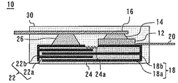
図1は、本発明の実施の形態1に係る半導体装置の断面図である。半導体装置10は、半導体素子12を有している。半導体素子12は上面にエミッタが形成され下面にコレクタが形成されたIGBTである。半導体素子12の上面には、はんだ14を介して第1電極16が電気的に接続されている。第1電極16はエミッタ電極として機能する。
FIG. 1 is a cross-sectional view of a semiconductor device according to
半導体素子12の下面には、第1内部電極18が電気的に接続されている。第1内部電極18は、複数の第1櫛歯部18aと複数の第1櫛歯部18aを連結する第1連結部18bとを有している。複数の第1櫛歯部18aの櫛歯部はそれぞれ平行に伸びている。複数の第1櫛歯部の1つの櫛歯が半導体素子12の下面と面接触している。
A first
第1内部電極18には第2電極20が電気的に接続されている。第2電極20はコレクタ電極として機能する。第1内部電極18と対向する位置に第2内部電極22が形成されている。第2内部電極22は、複数の第2櫛歯部22aと複数の第2櫛歯部22aを連結する第2連結部22bとを有している。複数の第2櫛歯部22aの櫛歯部はそれぞれ平行に伸びている。複数の第2櫛歯部22aは複数の第1櫛歯部18aに接触せず複数の第1櫛歯部18aの間に進入している。すなわち、複数の第1櫛歯部18aと複数の第2櫛歯部22aは、接触せずにかみ合うように配置されている。
A
複数の第1櫛歯部18aと複数の第2櫛歯部22aの間は下部誘電体24で埋められている。下部誘電体24はセラミックで形成されている。これにより下部誘電体24、複数の第1櫛歯部18a、及び複数の第2櫛歯部22aを有し、複数の第1櫛歯部18aと複数の第2櫛歯部22aを電極とするコンデンサが形成されている。なお、下部誘電体24には凹部24aが形成されている。
A space between the plurality of first
第2内部電極22は、第1電極16の下面に電気的に接続されている。具体的には、複数の第2櫛歯部22aの1つの櫛歯がはんだ26を介して第1電極16の下面と電気的に接続されている。半導体素子12、第1内部電極18、及び第2内部電極22を覆い、第1電極16の一部、第2電極20の一部、及び下部誘電体24の一部を外部に露出させる樹脂30が形成されている。樹脂30は、トランスファーモールド法で形成されたものである。前述の凹部24aは樹脂30と接する部分に形成されているため、凹部24aには樹脂30が満たされている。
The second
図2は、本発明の実施の形態1に係る半導体装置10の搭載例を示す斜視図である。半導体装置10は、冷却体50の上の接合材52によって冷却体50と固定される。そして、下部誘電体24の下面が熱伝導材54と接触することで、半導体装置10の放熱性を高めることができる。
FIG. 2 is a perspective view showing an example of mounting the
下部誘電体24は、絶縁膜として半導体素子12を半導体装置10の外部から絶縁する。これにより半導体素子12と冷却体50を絶縁できる。さらに下部誘電体24は、前述の通りコンデンサの電極間材料としても機能する。すなわち、下部誘電体24は、半導体素子12の絶縁膜としての機能と、コンデンサの誘電体としての機能を併せ持つ。また、本発明の実施の形態1に係る半導体装置10は、樹脂30内部において半導体素子12とコンデンサを隣接させたため半導体素子12とコンデンサを十分に近接させて低インダクタンスとすることができる。しかも、半導体素子12とコンデンサをトランスファーモールド法で一体的に重ねて形成したので半導体装置10の設置面積を低減して冷却体などへの搭載性を高めることができる。
The
また、半導体装置10の下部から冷却することにより、コンデンサと半導体素子12の両方を冷却することが可能となる。なお、凹部24aに樹脂を満たすことで樹脂30の剥がれを防止するアンカー効果をもたせることができる。
Further, by cooling from the lower part of the
ところで、本発明の実施の形態1に係る半導体装置10は様々な用途がある。例えば半導体装置10を用いてブリッジ回路を構成することができる。図3は、本発明の実施の形態1に係る半導体装置でハーフブリッジ回路を構成したことを示す図である。半導体装置10の第1内部電極18、下部誘電体24、及び第2内部電極22からなるコンデンサは整流コンデンサC1として用いることができる。
Incidentally, the
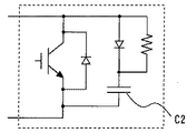
また、半導体装置10でスナバ回路を構成することもできる。図4は、本発明の実施の形態1に係る半導体装置でCRDスナバ回路を構成したことを示す図である。第1内部電極18、下部誘電体24、及び第2内部電極22からなるコンデンサをスナバ回路のコンデンサC2として用いることができる。
In addition, a snubber circuit can be configured by the
本発明の実施の形態1に係る半導体装置の下部誘電体24はセラミック以外の材料で形成してもよい。下部誘電体24は、絶縁体と誘電体の両方の性質を有するもので形成されれば特に限定されない。例えば下部誘電体をセラミック以外の無機物で形成してもよいし、樹脂フィルム等の有機物で形成してもよい。
The
本発明の実施の形態1に係る半導体装置の凹部24aは、下部誘電体24に限らず第1内部電極18又は第2内部電極22の樹脂30と接する部分に形成してもよい。凹部を形成する部分を増やすことで、樹脂の剥がれを防止する効果を高めることができる。
The
実施の形態2.
図5は、本発明の実施の形態2に係る半導体装置の断面図である。実施の形態1との相違点を中心に説明する。本発明の実施の形態2に係る半導体装置は、第3内部電極60を有している。第3内部電極60は、複数の第3櫛歯部60aと複数の第3櫛歯部60aを連結する第3連結部60bとを有している。第3内部電極60は、はんだ62を介して第2電極20に電気的に接続されている。具体的には複数の第3櫛歯部60aの1つの櫛歯がはんだを介して第2電極20の上面に接続されている。なお、第3内部電極60は、半導体素子12の上面側に形成されている。
Embodiment 2. FIG.
FIG. 5 is a cross-sectional view of the semiconductor device according to the second embodiment of the present invention. The description will focus on the differences from the first embodiment. The semiconductor device according to the second embodiment of the present invention has a third
第3内部電極60と対向する位置に第4内部電極64が形成されている。第4内部電極64は、複数の第3櫛歯部60aに接触せず複数の第3櫛歯部60aの間に進入する複数の第4櫛歯部64aと、複数の第4櫛歯部64aを連結する第4連結部64bとを有している。第4内部電極64は、第1電極16の上面に電気的に接続されている。具体的には、複数の第4櫛歯部64aの1つの櫛歯が第1電極16の上面に面接触している。
A fourth
さらに、上部誘電体66が複数の第3櫛歯部60aと複数の第4櫛歯部64aの間を埋めている。これにより上部誘電体66、複数の第3櫛歯部60a、及び複数の第4櫛歯部64aを有し、複数の第3櫛歯部60aと複数の第4櫛歯部64aを電極とするコンデンサが形成されている。
Further, the
樹脂30は、半導体素子12、第1内部電極18、第2内部電極22、第3内部電極60、及び第4内部電極64を覆い、第1電極16の一部、第2電極20の一部、下部誘電体24の一部、及び上部誘電体66の一部を外部に露出させている。
The
本発明の実施の形態2に係る半導体装置によれば、半導体装置の下面と上面の両方から誘電体が露出しているので、半導体装置の下面と上面の両方から半導体装置を冷却することができる。また、半導体素子12の上側と下側にコンデンサを形成したので、コンデンサの容量設定の自由度を高くすることができる。
According to the semiconductor device according to the second embodiment of the present invention, since the dielectric is exposed from both the lower surface and the upper surface of the semiconductor device, the semiconductor device can be cooled from both the lower surface and the upper surface of the semiconductor device. . In addition, since the capacitors are formed on the upper side and the lower side of the
なお、本発明の実施の形態2に係る半導体装置は、少なくとも実施の形態1と同程度の変形や応用が可能である。例えば、下部誘電体24と上部誘電体66を樹脂フィルムで形成してもよい。
It should be noted that the semiconductor device according to the second embodiment of the present invention can be modified and applied at least as much as the first embodiment. For example, the
実施の形態3.
図6は、本発明の実施の形態3に係る半導体装置の断面図である。実施の形態1との相違点を中心に説明する。第1内部電極100と第2内部電極102は上下方向に対向している。具体的には、第1連結部100bは半導体素子12の下面と面接触している。また、複数の第1櫛歯部100aは第1連結部100bから下方に伸びている。第2連結部102bの上面は第1連結部100bに対向している。そして、複数の第2櫛歯部102aは第2連結部102bから上方に伸びている。
Embodiment 3 FIG.
FIG. 6 is a cross-sectional view of the semiconductor device according to the third embodiment of the present invention. The description will focus on the differences from the first embodiment. The first
第1電極104は、はんだ14を介して半導体素子12の上面と電気的に接続されるとともに第2連結部102bの上面と面接触するように、屈曲した形状である。樹脂30は、半導体素子12、及び第1内部電極100を覆い、第1電極104の一部、第2電極20の一部、第2連結部102bの下面を外部に露出させるように形成されている。
The
本発明の実施の形態3に係る半導体装置によれば、複数の第1櫛歯部100aが第1連結部100bから下方に伸び、複数の第2櫛歯部102aは第2連結部102bから上方に伸び、第2連結部102bの下面は外部に露出している。よって、半導体素子12で発生した熱を速やかに外部に逃がすことができるので、半導体装置の放熱性を高めることができる。なお本発明の実施の形態3に係る半導体装置は、少なくとも実施の形態1と同程度の変形や応用が可能である。
According to the semiconductor device according to the third embodiment of the present invention, the plurality of
実施の形態4.
図7は、本発明の実施の形態4に係る半導体装置の断面図である。実施の形態3との相違点を中心に説明する。本発明の実施の形態4に係る半導体装置は、第3内部電極124を有している。第3内部電極124は、複数の第3櫛歯部124aと複数の第3櫛歯部を連結する第3連結部124bとを有している。第3内部電極124は、はんだ126を介して第2電極20の上面に電気的に接続されている。この第3内部電極124は、半導体素子12の上面側に形成されている。
Embodiment 4 FIG.
FIG. 7 is a cross-sectional view of a semiconductor device according to Embodiment 4 of the present invention. The difference from the third embodiment will be mainly described. The semiconductor device according to the fourth embodiment of the present invention has a third
第3内部電極124と対向する位置に第4内部電極128が形成されている。第4内部電極128は、複数の第3櫛歯部124aに接触せず複数の第3櫛歯部124aの間に進入する複数の第4櫛歯部128aと、複数の第4櫛歯部128aを連結する第4連結部128bとを有している。第4内部電極128は、はんだ130を介して第1電極104の上面に電気的に接続されている。具体的には、第4連結部128bの下面ははんだ130により第1電極104の上面と電気的に接続されている。
A fourth
上部誘電体132は、複数の第3櫛歯部124aと複数の第4櫛歯部128aの間を埋めている。これにより上部誘電体132、複数の第3櫛歯部124a、及び複数の第4櫛歯部128aを有し、複数の第3櫛歯部124aと複数の第4櫛歯部128aを電極とするコンデンサが形成される。
The
樹脂30は、半導体素子12、第1内部電極100、第4内部電極128を覆い、第1電極104の一部、第2電極20の一部、第2連結部102bの下面、及び第3連結部124bの上面を外部に露出させている。
The
本発明の実施の形態4に係る半導体装置は、実施の形態3に係る半導体装置の半導体素子の上方にコンデンサを追加したものである。従って、本発明の実施の形態4に係る半導体装置によれば、半導体装置の下面と上面の両方から冷却することができる。半導体素子の上方では、複数の第4櫛歯部128aが第4連結部128bから上方に伸び、第3連結部124bの下面は第4連結部128bに対向し、複数の第3櫛歯部124aが第3連結部124bから下方に伸びているので放熱が容易となる。
The semiconductor device according to the fourth embodiment of the present invention is obtained by adding a capacitor above the semiconductor element of the semiconductor device according to the third embodiment. Therefore, the semiconductor device according to the fourth embodiment of the present invention can be cooled from both the lower surface and the upper surface of the semiconductor device. Above the semiconductor element, a plurality of
また、半導体素子12の上側と下側にコンデンサを形成したので、コンデンサの容量設定の自由度を高くすることができる。なお本発明の実施の形態4に係る半導体装置は、少なくとも実施の形態1、3と同程度の変形や応用が可能である。
In addition, since the capacitors are formed on the upper side and the lower side of the
10 半導体装置、 12 半導体素子、 14 はんだ、 16 第1電極、 18a 複数の第1櫛歯部、 18b 第1連結部、 18 第1内部電極、 20 第2電極、 22a 複数の第2櫛歯部、 22b 第2連結部、 22 第2内部電極、 24 下部誘電体、 24a 凹部、 30 樹脂、 50 冷却体、 52 接合材、 54 熱伝導材、 60a 複数の第3櫛歯部、 60b 第3連結部、 60 第3内部電極、 62 はんだ、 64a 複数の第4櫛歯部、 64b 第4連結部、 64 第4内部電極、 66 上部誘電体
DESCRIPTION OF
Claims (12)
前記半導体素子の上面に電気的に接続された第1電極と、
複数の第1櫛歯部と前記複数の第1櫛歯部を連結する第1連結部とを有し、前記半導体素子の下面に面接触した第1内部電極と、
前記第1内部電極と電気的に接続された第2電極と、
前記複数の第1櫛歯部に接触せず前記複数の第1櫛歯部の間に進入する複数の第2櫛歯部と、前記複数の第2櫛歯部を連結する第2連結部とを有し、前記第1電極の下面に電気的に接続された第2内部電極と、
前記複数の第1櫛歯部と前記複数の第2櫛歯部の間を埋める下部誘電体と、を備えたことを特徴とする半導体装置。 A semiconductor element;
A first electrode electrically connected to an upper surface of the semiconductor element;
A first internal electrode having a plurality of first comb teeth and a first connection that couples the plurality of first comb teeth, and being in surface contact with the lower surface of the semiconductor element;
A second electrode electrically connected to the first internal electrode;
A plurality of second comb teeth that enter between the plurality of first comb teeth without contacting the plurality of first comb teeth; and a second connection that connects the plurality of second comb teeth A second internal electrode electrically connected to the lower surface of the first electrode;
A semiconductor device comprising: a plurality of first comb teeth and a lower dielectric filling between the plurality of second comb teeth.
前記複数の第1櫛歯部の1つの櫛歯が前記半導体素子の下面と面接触したことを特徴とする請求項1に記載の半導体装置。 Resin that covers the semiconductor element, the first internal electrode, and the second internal electrode, and exposes a part of the first electrode, a part of the second electrode, and a part of the lower dielectric to the outside. Prepared,
The semiconductor device according to claim 1, wherein one comb tooth of the plurality of first comb tooth portions is in surface contact with a lower surface of the semiconductor element.
前記複数の第3櫛歯部に接触せず前記複数の第3櫛歯部の間に進入する複数の第4櫛歯部と、前記複数の第4櫛歯部を連結する第4連結部とを有し、前記第1電極の上面に電気的に接続された第4内部電極と、
前記複数の第3櫛歯部と前記複数の第4櫛歯部の間を埋める上部誘電体と、を備えたことを特徴とする請求項1に記載の半導体装置。 A plurality of third comb teeth and a third coupling portion that couples the plurality of third comb teeth; electrically connected to the second electrode; and formed on the upper surface side of the semiconductor element A third internal electrode;
A plurality of fourth comb teeth that enter between the plurality of third comb teeth without contacting the plurality of third comb teeth, and a fourth connection that connects the plurality of fourth comb teeth A fourth internal electrode electrically connected to the upper surface of the first electrode;
2. The semiconductor device according to claim 1, further comprising an upper dielectric that fills a space between the plurality of third comb teeth and the plurality of fourth comb teeth.
前記第1連結部は前記半導体素子の下面と面接触し、
前記複数の第1櫛歯部は前記第1連結部から下方に伸び、
前記第2連結部の上面は前記第1連結部に対向し、
前記樹脂は、前記第2連結部の下面を外部に露出させることを特徴とする請求項1に記載の半導体装置。 A resin covering the semiconductor element and the first internal electrode, and exposing a part of the first electrode and a part of the second electrode to the outside;
The first connecting portion is in surface contact with the lower surface of the semiconductor element;
The plurality of first comb teeth extend downward from the first coupling portion,
The upper surface of the second connecting part faces the first connecting part,
The semiconductor device according to claim 1, wherein the resin exposes a lower surface of the second connecting portion to the outside.
前記第1連結部は前記半導体素子の下面と面接触し、
前記複数の第1櫛歯部は前記第1連結部から下方に伸び、
前記第2連結部の上面は前記第1連結部に対向し
前記第4連結部の下面は前記第1電極の上面と対向しつつ電気的に接続され、
前記複数の第4櫛歯部は前記第4連結部から上方に伸び、
前記第3連結部の下面は前記第4連結部に対向し、
前記樹脂は前記第2連結部の下面、及び前記第3連結部の上面を外部に露出させることを特徴とする請求項3に記載の半導体装置。 A resin covering the semiconductor element, the first internal electrode, and the fourth internal electrode, and exposing a part of the first electrode and a part of the second electrode to the outside;
The first connecting portion is in surface contact with the lower surface of the semiconductor element;
The plurality of first comb teeth extend downward from the first coupling portion,
The upper surface of the second connecting portion is opposed to the first connecting portion, and the lower surface of the fourth connecting portion is electrically connected while facing the upper surface of the first electrode,
The plurality of fourth comb teeth extend upward from the fourth connecting portion,
The lower surface of the third connecting part faces the fourth connecting part,
The semiconductor device according to claim 3, wherein the resin exposes a lower surface of the second connecting portion and an upper surface of the third connecting portion to the outside.
前記凹部に前記樹脂が満たされたことを特徴とする請求項2に記載の半導体装置。 The lower dielectric, the first internal electrode, or the second internal electrode has a recess in a portion in contact with the resin,
The semiconductor device according to claim 2, wherein the recess is filled with the resin.
前記冷却体の上に設けられた熱伝導材と、を備え、 A heat conductive material provided on the cooling body,
前記下部誘電体の下面が前記熱伝導材に接触することを特徴とする請求項1に記載の半導体装置。 The semiconductor device according to claim 1, wherein a lower surface of the lower dielectric is in contact with the heat conductive material.
Priority Applications (4)
| Application Number | Priority Date | Filing Date | Title |
|---|---|---|---|
| JP2012053061A JP5754398B2 (en) | 2012-03-09 | 2012-03-09 | Semiconductor device |
| DE102012224354.2A DE102012224354B4 (en) | 2012-03-09 | 2012-12-21 | Semiconductor device |
| US13/733,723 US8754462B2 (en) | 2012-03-09 | 2013-01-03 | Semiconductor device |
| CN201310074184.1A CN103311191B (en) | 2012-03-09 | 2013-03-08 | Semiconductor device |
Applications Claiming Priority (1)
| Application Number | Priority Date | Filing Date | Title |
|---|---|---|---|
| JP2012053061A JP5754398B2 (en) | 2012-03-09 | 2012-03-09 | Semiconductor device |
Publications (3)
| Publication Number | Publication Date |
|---|---|
| JP2013187464A JP2013187464A (en) | 2013-09-19 |
| JP2013187464A5 JP2013187464A5 (en) | 2014-10-09 |
| JP5754398B2 true JP5754398B2 (en) | 2015-07-29 |
Family
ID=49029640
Family Applications (1)
| Application Number | Title | Priority Date | Filing Date |
|---|---|---|---|
| JP2012053061A Active JP5754398B2 (en) | 2012-03-09 | 2012-03-09 | Semiconductor device |
Country Status (4)
| Country | Link |
|---|---|
| US (1) | US8754462B2 (en) |
| JP (1) | JP5754398B2 (en) |
| CN (1) | CN103311191B (en) |
| DE (1) | DE102012224354B4 (en) |
Families Citing this family (6)
| Publication number | Priority date | Publication date | Assignee | Title |
|---|---|---|---|---|
| WO2013140503A1 (en) * | 2012-03-19 | 2013-09-26 | 三菱電機株式会社 | Semiconductor device and semiconductor system |
| WO2015133024A1 (en) * | 2014-03-06 | 2015-09-11 | 三菱電機株式会社 | Power semiconductor device |
| WO2020218298A1 (en) * | 2019-04-24 | 2020-10-29 | ローム株式会社 | Semiconductor device |
| US20220165719A1 (en) | 2019-04-24 | 2022-05-26 | Rohm Co., Ltd. | Semiconductor device |
| US11538748B2 (en) | 2020-06-04 | 2022-12-27 | Mediatek Singapore Pte. Ltd. | Semiconductor device with capacitor element |
| DE102022211040A1 (en) | 2022-10-19 | 2024-04-25 | Robert Bosch Gesellschaft mit beschränkter Haftung | Semiconductor module |
Family Cites Families (23)
| Publication number | Priority date | Publication date | Assignee | Title |
|---|---|---|---|---|
| JPH05299584A (en) | 1992-02-21 | 1993-11-12 | Toshiba Corp | Thin film capacitor element and semiconductor memory device |
| JPH06140446A (en) | 1992-07-21 | 1994-05-20 | Hitachi Ltd | Semiconductor device and electronic device using same |
| JP3340003B2 (en) * | 1995-11-20 | 2002-10-28 | 京セラ株式会社 | Multilayer wiring board and package for housing semiconductor element |
| JPH10174424A (en) | 1996-10-07 | 1998-06-26 | Toshiba Corp | Power converter |
| JP2000058372A (en) | 1998-08-04 | 2000-02-25 | Toshiba Corp | Ceramic capacitor mounting structure |
| JP2000092847A (en) | 1998-09-14 | 2000-03-31 | Denso Corp | Semiconductor module apparatus with capacitor |
| JP3553849B2 (en) | 2000-03-07 | 2004-08-11 | 富士電機デバイステクノロジー株式会社 | Semiconductor device and manufacturing method thereof |
| JP4044265B2 (en) | 2000-05-16 | 2008-02-06 | 三菱電機株式会社 | Power module |
| US6558169B2 (en) * | 2001-03-29 | 2003-05-06 | Intel Corporation | Shunt power connection for an integrated circuit package |
| JP4060657B2 (en) * | 2002-07-18 | 2008-03-12 | Necトーキン株式会社 | Solid electrolytic capacitor and manufacturing method thereof |
| JP2004350400A (en) | 2003-05-22 | 2004-12-09 | Hitachi Ltd | Power converter |
| DE10345247B4 (en) | 2003-09-29 | 2007-10-04 | Infineon Technologies Ag | Use of conductor tracks as Krallkörper |
| JP2005341643A (en) * | 2004-05-24 | 2005-12-08 | Toshiba Corp | Bus bar apparatus of power converter |
| JP2006174566A (en) * | 2004-12-14 | 2006-06-29 | Toyota Motor Corp | Current control element, booster and inverter device |
| JP2006222347A (en) * | 2005-02-14 | 2006-08-24 | Toyota Motor Corp | Semiconductor module and manufacturing method thereof |
| JP4661645B2 (en) * | 2005-03-23 | 2011-03-30 | トヨタ自動車株式会社 | Power semiconductor module |
| KR100876247B1 (en) * | 2006-10-19 | 2008-12-26 | 삼성에스디아이 주식회사 | Secondary Battery and Manufacturing Method Thereof |
| JP5061717B2 (en) | 2007-05-18 | 2012-10-31 | 富士電機株式会社 | Semiconductor module and method for manufacturing semiconductor module |
| JP5151338B2 (en) * | 2007-09-14 | 2013-02-27 | 株式会社Ihi | Insulated semiconductor power module with built-in capacitor |
| US8053865B2 (en) * | 2008-03-10 | 2011-11-08 | Taiwan Semiconductor Manufacturing Company, Ltd. | MOM capacitors integrated with air-gaps |
| JP5169353B2 (en) * | 2008-03-18 | 2013-03-27 | 三菱電機株式会社 | Power module |
| JP5332753B2 (en) | 2009-03-10 | 2013-11-06 | 日産自動車株式会社 | Mechanical and electric integrated drive |
| JP5469584B2 (en) | 2010-10-28 | 2014-04-16 | 株式会社日立製作所 | Built-in capacitor between bus bars, power equipment and power converter |
-
2012
- 2012-03-09 JP JP2012053061A patent/JP5754398B2/en active Active
- 2012-12-21 DE DE102012224354.2A patent/DE102012224354B4/en active Active
-
2013
- 2013-01-03 US US13/733,723 patent/US8754462B2/en active Active
- 2013-03-08 CN CN201310074184.1A patent/CN103311191B/en active Active
Also Published As
| Publication number | Publication date |
|---|---|
| US8754462B2 (en) | 2014-06-17 |
| US20130234291A1 (en) | 2013-09-12 |
| CN103311191B (en) | 2016-08-10 |
| CN103311191A (en) | 2013-09-18 |
| DE102012224354B4 (en) | 2021-09-30 |
| JP2013187464A (en) | 2013-09-19 |
| DE102012224354A1 (en) | 2013-09-12 |
Similar Documents
| Publication | Publication Date | Title |
|---|---|---|
| JP6230660B2 (en) | Power semiconductor module | |
| US9871463B2 (en) | Power module | |
| JP5754398B2 (en) | Semiconductor device | |
| JP6233507B2 (en) | Power semiconductor modules and composite modules | |
| JP4613077B2 (en) | Semiconductor device, electrode member, and method for manufacturing electrode member | |
| KR101581610B1 (en) | Semiconductor device and method for manufacturing same | |
| EP3104412B1 (en) | Power semiconductor module | |
| JP5678884B2 (en) | Power converter | |
| JP2007073743A (en) | Semiconductor device | |
| US8373197B2 (en) | Circuit device | |
| WO2015072105A1 (en) | Power module | |
| IT201800004209A1 (en) | SEMICONDUCTIVE POWER DEVICE WITH RELATIVE ENCAPSULATION AND CORRESPONDING MANUFACTURING PROCEDURE | |
| JP2009010252A (en) | Semiconductor device | |
| KR101734712B1 (en) | Power module | |
| JP6813259B2 (en) | Semiconductor device | |
| JP7176397B2 (en) | Semiconductor device and its manufacturing method | |
| JP5619232B2 (en) | Semiconductor device and method for manufacturing electrode member | |
| WO2021029150A1 (en) | Semiconductor device | |
| JP5151338B2 (en) | Insulated semiconductor power module with built-in capacitor | |
| JP7155748B2 (en) | semiconductor equipment | |
| JP5485833B2 (en) | Semiconductor device, electrode member, and method for manufacturing electrode member | |
| JP7118204B1 (en) | semiconductor equipment | |
| KR20190085587A (en) | High thermal conductivity semiconductor package | |
| WO2024024067A1 (en) | Electric power conversion device, and method for producing electric power conversion device | |
| JP2016214012A (en) | Power conversion device |
Legal Events
| Date | Code | Title | Description |
|---|---|---|---|
| A521 | Request for written amendment filed |
Free format text: JAPANESE INTERMEDIATE CODE: A523 Effective date: 20140430 |
|
| A621 | Written request for application examination |
Free format text: JAPANESE INTERMEDIATE CODE: A621 Effective date: 20140430 |
|
| A521 | Request for written amendment filed |
Free format text: JAPANESE INTERMEDIATE CODE: A523 Effective date: 20140821 |
|
| A977 | Report on retrieval |
Free format text: JAPANESE INTERMEDIATE CODE: A971007 Effective date: 20141212 |
|
| A131 | Notification of reasons for refusal |
Free format text: JAPANESE INTERMEDIATE CODE: A131 Effective date: 20150106 |
|
| A521 | Request for written amendment filed |
Free format text: JAPANESE INTERMEDIATE CODE: A523 Effective date: 20150127 |
|
| TRDD | Decision of grant or rejection written | ||
| A01 | Written decision to grant a patent or to grant a registration (utility model) |
Free format text: JAPANESE INTERMEDIATE CODE: A01 Effective date: 20150428 |
|
| A61 | First payment of annual fees (during grant procedure) |
Free format text: JAPANESE INTERMEDIATE CODE: A61 Effective date: 20150511 |
|
| R150 | Certificate of patent or registration of utility model |
Ref document number: 5754398 Country of ref document: JP Free format text: JAPANESE INTERMEDIATE CODE: R150 |
|
| R250 | Receipt of annual fees |
Free format text: JAPANESE INTERMEDIATE CODE: R250 |
|
| R250 | Receipt of annual fees |
Free format text: JAPANESE INTERMEDIATE CODE: R250 |
|
| R250 | Receipt of annual fees |
Free format text: JAPANESE INTERMEDIATE CODE: R250 |
|
| R250 | Receipt of annual fees |
Free format text: JAPANESE INTERMEDIATE CODE: R250 |
|
| R250 | Receipt of annual fees |
Free format text: JAPANESE INTERMEDIATE CODE: R250 |
|
| R250 | Receipt of annual fees |
Free format text: JAPANESE INTERMEDIATE CODE: R250 |