JP5725397B2 - Electrochromic compound - Google Patents
Electrochromic compound Download PDFInfo
- Publication number
- JP5725397B2 JP5725397B2 JP2010172866A JP2010172866A JP5725397B2 JP 5725397 B2 JP5725397 B2 JP 5725397B2 JP 2010172866 A JP2010172866 A JP 2010172866A JP 2010172866 A JP2010172866 A JP 2010172866A JP 5725397 B2 JP5725397 B2 JP 5725397B2
- Authority
- JP
- Japan
- Prior art keywords
- group
- display
- substituted
- electrochromic
- unsubstituted
- Prior art date
- Legal status (The legal status is an assumption and is not a legal conclusion. Google has not performed a legal analysis and makes no representation as to the accuracy of the status listed.)
- Expired - Fee Related
Links
Images


Description
本発明は、エレクトロクロミック化合物、エレクトロクロミック組成物、表示素子及び表示装置に関する。 The present invention relates to an electrochromic compound, an electrochromic composition, a display element, and a display device.
近年、紙に替わる電子媒体として、電子ペーパーが知られている。電子ペーパーは、表示装置が紙のように用いられる。 In recent years, electronic paper has been known as an electronic medium that replaces paper. Electronic paper is used like a paper display device.
電子ペーパー用途の表示装置としては、反射型液晶表示装置、電気泳動表示装置等が知られている。しかしながら、白反射率及びコントラスト比を確保しながら、多色表示することは大変困難である。一般に、多色表示するためには、カラーフィルタを設けるが、カラーフィルタが光を吸収することに加え、一画素を、例えば、レッド、グリーン及びブルーに3分割するため、白反射率が低下し、それに伴ってコントラスト比が低下する。 As display devices for electronic paper, reflection type liquid crystal display devices, electrophoretic display devices, and the like are known. However, it is very difficult to display multiple colors while ensuring white reflectance and contrast ratio. In general, a color filter is provided for multicolor display. In addition to the light absorbing by the color filter, one pixel is divided into, for example, red, green, and blue, so that the white reflectance decreases. As a result, the contrast ratio decreases.
一方、カラーフィルタを設けない反射型の表示装置として、エレクトロクロミック表示装置が知られている。エレクトロクロミック表示装置は、エレクトロクロミック化合物の構造によって様々な色を発色できるため、多色カラー表示装置として期待されている。 On the other hand, an electrochromic display device is known as a reflective display device without a color filter. An electrochromic display device is expected as a multicolor display device because it can generate various colors depending on the structure of the electrochromic compound.
特許文献1には、表示電極と、該表示電極に対して間隔をおいて対向して設けた対向電極と、両電極間に配置された電解質とを備え、該表示電極の対向電極側の表面に異なる色を発色し、かつ、発色状態になるための閾値電圧または消色状態になるための閾値電圧または十分な色濃度に発色するための必要電荷量または十分に消色するための必要電荷量のうち少なくともいずれかが異なる2種類以上のエレクトロクロミック組成物を積層または混合して形成した表示層を有することを特徴とする多色表示素子が開示されている。
しかしながら、エレクトロクロミック組成物に含まれるビオロゲン化合物は、青色、緑色等を発色するものであり、フルカラー化に必要なシアンを発色することができない。 However, the viologen compound contained in the electrochromic composition develops blue, green, and the like, and cannot develop cyan necessary for full color.
本発明は、上記従来技術が有する問題に鑑み、シアンを発色及び消色することが可能なエレクトロクロミック化合物及びエレクトロクロミック組成物並びに該エレクトロクロミック化合物又は該エレクトロクロミック組成物を有する表示素子及び表示装置を提供することを目的とする。 The present invention has been made in view of the above-described problems of the prior art, and an electrochromic compound and an electrochromic composition capable of developing and decoloring cyan, and a display element and a display device having the electrochromic compound or the electrochromic composition The purpose is to provide.
請求項1に記載の発明は、エレクトロクロミック化合物において、一般式
The invention according to

で表されることを特徴とする。
It is represented by.
請求項2に記載の発明は、請求項1に記載のエレクトロクロミック化合物において、前記アルキル基は、炭素数が2以上20以下であることを特徴とする。
The invention described in
請求項3に記載の発明は、エレクトロクロミック組成物において、導電性又は半導体性のナノスケールの凹凸を有する構造体に請求項1又は2に記載のエレクトロクロミック化合物が結合又は吸着されていることを特徴とする。 According to a third aspect of the present invention, in the electrochromic composition, the electrochromic compound according to the first or second aspect is bound or adsorbed to a structure having conductive or semiconducting nanoscale irregularities. Features.
請求項4に記載の発明は、エレクトロクロミック組成物において、導電性又は半導体性のナノスケールの凹凸を有する構造体に、一般式 In the electrochromic composition, the structure having conductive or semiconducting nanoscale unevenness has a general formula.
で表される化合物を反応させた後、一般式
After reacting the compound represented by general formula
で表される化合物を反応させることにより得られることを特徴とする。
It is obtained by reacting a compound represented by the formula:
請求項5に記載の発明は、表示電極と、前記表示電極に対して、所定の間隔を隔てて対向して設けられている対向電極と、前記表示電極及び前記対向電極の間に挟持されている電解質を有する表示素子であって、前記表示電極の前記対向電極側の表面に、請求項1若しくは2に記載のエレクトロクロミック化合物又は請求項3若しくは4に記載のエレクトロクロミック組成物を含む表示層が形成されていることを特徴とする。
The invention according to claim 5 is sandwiched between the display electrode, the counter electrode provided to face the display electrode at a predetermined interval, and the display electrode and the counter electrode. A display layer comprising an electrolyte that includes the electrochromic compound according to
請求項6に記載の発明は、表示装置において、請求項5に記載の表示素子と、前記表示素子を駆動する手段を有することを特徴とする。 According to a sixth aspect of the present invention, in the display device, the display element according to the fifth aspect and means for driving the display element are provided.
本発明によれば、シアンを発色及び消色することが可能なエレクトロクロミック化合物及びエレクトロクロミック組成物並びに該エレクトロクロミック化合物又は該エレクトロクロミック組成物を有する表示素子及び表示装置を提供することができる。 ADVANTAGE OF THE INVENTION According to this invention, the display element and display apparatus which have the electrochromic compound and electrochromic composition which can color-develop and decolorize cyan, and this electrochromic compound or this electrochromic composition can be provided.
次に、本発明を実施するための形態を図面と共に説明する。 Next, the form for implementing this invention is demonstrated with drawing.
本発明のエレクトロクロミック化合物は、一般式 The electrochromic compound of the present invention has the general formula
で表される。
It is represented by
X1、X2、X3、X4、X5、X6、X7、X8及びX9により、エレクトロクロミック化合物の溶媒に対する溶解性を付与することができる。これにより、エレクトロクロミック組成物又は表示素子を作製するプロセスが容易になる。また、本発明のエレクトロクロミック化合物は、シアンを発色することができるが、X1、X2、X3、X4、X5、X6、X7、X8及びX9を調整すると、イエローやマゼンタを発色することもできる。 X 1 , X 2 , X 3 , X 4 , X 5 , X 6 , X 7 , X 8 and X 9 can impart solubility of the electrochromic compound to the solvent. This facilitates the process of producing the electrochromic composition or display element. In addition, the electrochromic compound of the present invention can develop cyan, but if X 1 , X 2 , X 3 , X 4 , X 5 , X 6 , X 7 , X 8 and X 9 are adjusted, yellow And magenta.
なお、耐熱性、耐光性等の安定性を考慮すると、X1、X2、X3、X4、X5、X6、X7、X8及びX9は、それぞれ独立に、水素原子、ハロゲン基又は炭素数が1〜6の基であることが好ましい。 In consideration of stability such as heat resistance and light resistance, X 1 , X 2 , X 3 , X 4 , X 5 , X 6 , X 7 , X 8 and X 9 are each independently a hydrogen atom, It is preferably a halogen group or a group having 1 to 6 carbon atoms.
また、R1及びR2は、それぞれ独立に、置換若しくは無置換の炭素数が2〜20のアルキル基又は置換若しくは無置換のアリール基であることが好ましい。これにより、本発明のエレクトロクロミック化合物の溶解性を向上させることができる。その結果、本発明のエレクトロクロミック化合物の合成が容易となり、収率が向上することに加え、表示層を形成することが容易となる。また、R1及びR2の立体障害により、表示層における本発明のエレクトロクロミック化合物同士の会合を抑制することができ、会合による酸化還元反応の不具合を低減することができる。アルキル基は、直鎖状、分岐状及び環状のいずれであってもよいが、立体障害を考慮すると、分岐状であることが好ましい。 R 1 and R 2 are preferably each independently a substituted or unsubstituted alkyl group having 2 to 20 carbon atoms or a substituted or unsubstituted aryl group. Thereby, the solubility of the electrochromic compound of this invention can be improved. As a result, the electrochromic compound of the present invention can be easily synthesized and the yield can be improved, and the display layer can be easily formed. In addition, due to the steric hindrance of R 1 and R 2 , association between the electrochromic compounds of the present invention in the display layer can be suppressed, and defects in the oxidation-reduction reaction due to the association can be reduced. The alkyl group may be linear, branched or cyclic, but is preferably branched considering steric hindrance.
R1及びR2のアルキル基、アルケニル基、アルキニル基又はアリール基における置換基としては、特に限定されないが、アルキル基、アリール基、アルコキシ基、スルホン酸基、ホスホン酸基、リン酸基、カルボキシル基、トリクロロシリル基、トリアルコキシシリル基、モノクロロシリル基、モノアルコキシシリル基等が挙げられ、二種以上併用してもよい。中でも、炭素数が1〜4のアルキル基;フルオロ基、クロロ基、ブロモ基等のハロゲン基;トリフルオロメチル基、2,2,2−トリフルオロエチル基、ペンタフルオロエチル基等のハロゲン化アルキル基が好ましい。 The substituent in the alkyl group, alkenyl group, alkynyl group or aryl group of R 1 and R 2 is not particularly limited, but is an alkyl group, aryl group, alkoxy group, sulfonic acid group, phosphonic acid group, phosphoric acid group, carboxyl group. Group, a trichlorosilyl group, a trialkoxysilyl group, a monochlorosilyl group, a monoalkoxysilyl group, and the like, and two or more of them may be used in combination. Among them, alkyl groups having 1 to 4 carbon atoms; halogen groups such as fluoro groups, chloro groups, and bromo groups; halogenated alkyl groups such as trifluoromethyl groups, 2,2,2-trifluoroethyl groups, and pentafluoroethyl groups Groups are preferred.
1価のアニオンとしては、特に限定されないが、Br−、Cl−、ClO4 −、PF6 −、BF4 −等が挙げられる。 The monovalent anion is not particularly limited, and examples thereof include Br − , Cl − , ClO 4 − , PF 6 − and BF 4 − .
なお、本発明のエレクトロクロミック化合物は、合成の容易さ及び安定性の面から、対称的な構造であることが好ましい。 The electrochromic compound of the present invention preferably has a symmetric structure from the viewpoint of ease of synthesis and stability.
本発明のエレクトロクロミック化合物としては、特に限定されないが、エレクトロクロミック化合物(1)〜(11)が挙げられる。 Although it does not specifically limit as an electrochromic compound of this invention, Electrochromic compounds (1)-(11) are mentioned.
また、本発明のエレクトロクロミック組成物は、導電性又は半導体性のナノ構造体に、一般式 In addition, the electrochromic composition of the present invention has a general formula in a conductive or semiconducting nanostructure.
で表される化合物を反応させた後、一般式
After reacting the compound represented by general formula
で表される化合物を反応させることにより得られる。
It is obtained by reacting a compound represented by
一般式(2)で表される化合物は、導電性又は半導性のナノ構造体の表面のヒドロキシル基と反応し、シロキサン結合を介して結合することができる。このとき、導電性又は半導性のナノ構造体に対する結合力が大きいことから、C1、C2及びC3がエトキシ基、メトキシ基等のアルコキシ基又はクロロ基であることが好ましい。また、Aは、ブロモ基であることが好ましく、Bは、炭素数が1〜6のアルキレン基であることが好ましい。 The compound represented by the general formula (2) reacts with the hydroxyl group on the surface of the conductive or semiconductive nanostructure and can be bonded through a siloxane bond. At this time, C 1 , C 2, and C 3 are preferably an alkoxy group such as an ethoxy group or a methoxy group, or a chloro group, because the bonding strength to the conductive or semiconductive nanostructure is large. A is preferably a bromo group, and B is preferably an alkylene group having 1 to 6 carbon atoms.
X1、X2、X3、X4、X5、X6、X7、X8及びX9により、一般式(3)で表される化合物の溶媒に対する溶解性を付与することができる。これにより、エレクトロクロミック組成物又は表示素子を作製するプロセスが容易になる。また、本発明のエレクトロクロミック組成物は、シアンを発色することができるが、X1、X2、X3、X4、X5、X6、X7、X8及びX9を調整すると、イエローやマゼンタを発色することもできる。 X 1 , X 2 , X 3 , X 4 , X 5 , X 6 , X 7 , X 8 and X 9 can impart solubility to the solvent of the compound represented by the general formula (3). This facilitates the process of producing the electrochromic composition or display element. The electrochromic composition of the present invention can develop cyan, but when X 1 , X 2 , X 3 , X 4 , X 5 , X 6 , X 7 , X 8 and X 9 are adjusted, Yellow and magenta can also be developed.
なお、耐熱性、耐光性等の安定性を考慮すると、X1、X2、X3、X4、X5、X6、X7、X8及びX9は、それぞれ独立に、水素原子、ハロゲン基又は炭素数が1〜6の基であることが好ましい。 In consideration of stability such as heat resistance and light resistance, X 1 , X 2 , X 3 , X 4 , X 5 , X 6 , X 7 , X 8 and X 9 are each independently a hydrogen atom, It is preferably a halogen group or a group having 1 to 6 carbon atoms.
また、一般式(3)で表される化合物は、合成の容易さ及び安定性の面から、対称的な構造であることが好ましい。 Moreover, it is preferable that the compound represented by General formula (3) is a symmetrical structure from the surface of the synthetic | combination ease and stability.
このようにして得られる本発明のエレクトロクロミック組成物を含む表示層を有する表示素子は、画像のメモリ性、即ち、画像保持特性に優れる。 The display element having a display layer containing the electrochromic composition of the present invention thus obtained is excellent in image memory properties, that is, image retention characteristics.
導電性又は半導性のナノ構造体は、比表面積が100m2/g以上であることが好ましい。これにより、エレクトロクロミック化合物で効率的に表面処理することができ、発消色の表示コントラスト比に優れた多色表示が可能となる。 The conductive or semiconducting nanostructure preferably has a specific surface area of 100 m 2 / g or more. Thereby, the surface treatment can be efficiently performed with the electrochromic compound, and multicolor display excellent in the display contrast ratio of color development and decoloration is possible.
導電性又は半導性のナノ構造体としては、特に限定されないが、ナノ粒子集積体、ナノポーラス構造体等のナノスケールの凹凸を有する構造体が挙げられる。ナノ粒子は、平均一次粒径が30nm以下であることが好ましい。これにより、光の透過率が向上し、比表面積が大きくなる。 The conductive or semiconducting nanostructure is not particularly limited, and examples thereof include structures having nanoscale irregularities such as nanoparticle aggregates and nanoporous structures. The nanoparticles preferably have an average primary particle size of 30 nm or less. This improves the light transmittance and increases the specific surface area.
導電性又は半導性のナノ構造体は、透明性や導電性の面から、金属酸化物を含むことが好ましい。金属酸化物としては、特に限定されないが、酸化チタン、酸化亜鉛、酸化スズ、アルミナ、酸化ジルコニウム、酸化セリウム、シリカ、酸化イットリウム、酸素ホウ素、酸化マグネシウム、チタン酸ストロンチウム、チタン酸カリウム、チタン酸バリウム、チタン酸カルシウム、酸化カルシウム、フェライト、酸化ハフニウム、酸化タングステン、酸化鉄、酸化銅、酸化ニッケル、酸化コバルト、酸化バリウム、酸化ストロンチウム、酸化バナジウム、アルミノケイ酸、リン酸カルシウム、アルミノシリケート等が挙げられ、二種以上併用してもよい。中でも、発消色の応答速度に優れた多色表示が可能であることから、酸化チタン、酸化亜鉛、酸化スズ、アルミナ、酸化ジルコニウム、酸化鉄、酸化マグネシウム、酸化インジウム又は酸化タングステンが好ましく、酸化チタンが特に好ましい。 The conductive or semiconducting nanostructure preferably contains a metal oxide in terms of transparency and conductivity. The metal oxide is not particularly limited, but titanium oxide, zinc oxide, tin oxide, alumina, zirconium oxide, cerium oxide, silica, yttrium oxide, oxygen boron, magnesium oxide, strontium titanate, potassium titanate, barium titanate. , Calcium titanate, calcium oxide, ferrite, hafnium oxide, tungsten oxide, iron oxide, copper oxide, nickel oxide, cobalt oxide, barium oxide, strontium oxide, vanadium oxide, aluminosilicate, calcium phosphate, aluminosilicate, etc. Two or more species may be used in combination. Among these, titanium oxide, zinc oxide, tin oxide, alumina, zirconium oxide, iron oxide, magnesium oxide, indium oxide or tungsten oxide are preferable because multicolor display excellent in response speed of color development and decoloration is possible. Titanium is particularly preferred.
図1に、本発明の表示素子の一例を示す。表示素子10は、表示電極11aが形成されている表示基板11と、表示電極11aに対して、所定の間隔を隔てて対向して設けられている対向電極12aが形成されている対向基板12と、表示基板11及び対向基板12の間に挟持されている表示層13を有する。このとき、表示層13は、電解液13a中に本発明のエレクトロクロミック化合物13bが溶解されている。このとき、エレクトロクロミック化合物13bは、表示電極11の表面で酸化還元反応することにより発消色する。また、対向電極12の表示電極11側の表面に、白色粒子を含む白色反射層14が形成されているため、表示素子10は、反射型の表示素子である。なお、表示基板11及び対向基板12は、スペーサ15を介して、貼り合わされている。
FIG. 1 shows an example of the display element of the present invention. The
図2に、表示素子10の変形例を示す。表示素子20は、表示層13の代わりに、表示電極11aの対向電極12a側の表面に、エレクトロクロミック化合物13bを含む表示層23が形成されている以外は、表示素子10と同一の構成である。表示層23は、ディッピング法、蒸着法、スピンコート法、印刷法、インクジェット法等を用いて形成することができる。なお、R1及び/又はR2がスルホン酸基、ホスホン酸基、リン酸基、カルボキシル基、トリクロロシリル基、トリアルコキシシリル基、モノクロロシリル基及びモノアルコキシシリル基からなる群より選択される一種以上の官能基で置換されている場合、表面にヒドロキシル基を有する表示電極11aをエレクトロクロミック化合物13bで表面処理することができる。
FIG. 2 shows a modification of the
図3に、表示素子10の変形例を示す。表示素子30は、表示層13の代わりに、表示電極11aの対向電極12b側の表面に、本発明のエレクトロクロミック組成物33bを含む表示層33が形成されている以外は、表示素子10と同一の構成である。表示層33は、ディッピング法、蒸着法、スピンコート法、印刷法、インクジェット法等を用いて形成することができる。
FIG. 3 shows a modification of the
表示基板11は、表示電極11aが形成されている透明基板11bである。
The
表示電極11aを構成する材料としては、透明であれば、特に限定されないが、スズをドープした酸化インジウム(以下、ITOという)、フッ素をドープした酸化スズ(以下、FTOという)、アンチモンをドープした酸化スズ(以下、ATOという)等の無機材料が挙げられる。中でも、スパッタ法を用いて、容易に薄膜を形成できることから、インジウム酸化物、スズ酸化物又は亜鉛酸化物を含む無機材料が好ましく、InSnO、GaZnO、SnO、In2O3、ZnOが特に好ましい。
The material constituting the
透明基板11bを構成する材料としては、ガラス、プラスチック等が挙げられる。このとき、透明基板11bとして、プラスチックフィルムを用いると、軽量でフレキシブルな表示素子を作製することができる。
Examples of the material constituting the
対向基板12は、対向電極12aが形成されている基板12bである。
The
対向電極12aを構成する材料としては、特に限定されないが、ITO、FTO、酸化亜鉛、亜鉛、白金、カーボン等が挙げられる。このとき、対向電極12aが、エレクトロクロミック化合物が酸化(又は還元)するときに、還元(又は酸化)する材料を含むと、安定に発色及び消色することが可能な表示素子が得られる。
Although it does not specifically limit as a material which comprises the
基板12bを構成する材料としては、ガラス、プラスチック等が挙げられる。
Examples of the material constituting the
なお、対向基板12の代わりに、亜鉛板等の金属板を用いてもよい。
Instead of the
電解液13aとしては、支持塩を溶媒に溶解させた溶液、イオン液体等が用いられる。このため、イオン伝導度が高い。
As the
支持塩としては、特に限定されないが、LiClO4、LiBF4、LiAsF6、LiPF6、CF3SO3Li、CF3COOLi、KCl、NaClO3、NaCl、NaBF4、NaSCN、KBF4、Mg(ClO4)2、Mg(BF4)2等の金属塩;過塩素酸テトラブチルアンモニウム、テトラブチルアンモニウムヘキサフルオロホスファート等の4級アンモニウム塩等が挙げられる。 The supporting salt is not particularly limited, but LiClO 4 , LiBF 4 , LiAsF 6 , LiPF 6 , CF 3 SO 3 Li, CF 3 COOLi, KCl, NaClO 3 , NaCl, NaBF 4 , NaSCN, KBF 4 , Mg (ClO 4 ) 2 , metal salts such as Mg (BF 4 ) 2 ; quaternary ammonium salts such as tetrabutylammonium perchlorate and tetrabutylammonium hexafluorophosphate.
溶媒としては、特に限定されないが、プロピレンカーボネート、アセトニトリル、γ−ブチロラクトン、エチレンカーボネート、スルホラン、ジオキソラン、テトラヒドロフラン、2−メチルテトラヒドロフラン、ジメチルスルホキシド、1,2−ジメトキシエタン、1,2−エトキシメトキシエタン、ポリエチレングリコール、アルコール類等が挙げられる。 The solvent is not particularly limited, but propylene carbonate, acetonitrile, γ-butyrolactone, ethylene carbonate, sulfolane, dioxolane, tetrahydrofuran, 2-methyltetrahydrofuran, dimethyl sulfoxide, 1,2-dimethoxyethane, 1,2-ethoxymethoxyethane, Examples include polyethylene glycol and alcohols.
なお、電解液13aの代わりに、ゲル状の電解質;ポリマー電解質等の固体電解質を用いてもよい。ポリマー電解質としては、パーフルオロスルホン酸系高分子等が挙げられる。これにより、耐久性に優れる表示素子を作製することができる。
Instead of the
白色反射層14は、白色の顔料粒子及び樹脂を含む塗布液を対向電極12上に塗布することにより形成することができる。
The white
白色の顔料粒子としては、特に限定されないが、酸化チタン、酸化アルミニウム、酸化亜鉛、酸化ケイ素、酸化セシウム、酸化イットリウム等の金属酸化物が挙げられる。 Although it does not specifically limit as a white pigment particle, Metal oxides, such as a titanium oxide, an aluminum oxide, a zinc oxide, a silicon oxide, a cesium oxide, an yttrium oxide, are mentioned.
白色の顔料粒子は、反射率を考慮すると、平均粒径が50〜400nmであることが好ましい。 The white pigment particles preferably have an average particle size of 50 to 400 nm in consideration of reflectance.
なお、白色反射層14を形成する代わりに、ポリマー電解質中に白色の顔料粒子を分散させてもよい。
Instead of forming the white
表示素子10、20、30を駆動する方法としては、表示電極11aと対向電極12aの間に、所定の電圧を印加することが可能であれば、特に限定されない。このとき、パッシブ駆動する方法を用いると、安価な表示装置が得られる。また、アクティブ駆動する方法を用いると、高速で、高精細に表示することが可能な表示装置が得られる。なお、対向基板12にアクティブ駆動素子を設けることにより、容易にアクティブ駆動することができる。
A method for driving the
表示素子10、20、30は、電子書籍、電子看板、電子棚札等の表示装置に適用することができる。
The
(実施例1)
[エレクトロクロミック化合物(2)の合成]
図4に、エレクトロクロミック化合物(2)の合成フローを示す。
Example 1
[Synthesis of Electrochromic Compound (2)]
FIG. 4 shows a synthesis flow of the electrochromic compound (2).
4−アセチルピリジン5.6g、イソニコチン酸エチル7.0g及び1,4−ジオキサン30mlを反応フラスコに仕込み、カリウムtert−ブトキシド5.2gを徐々に加えた後、90℃で1時間撹拌し、放冷した。反応液を水80mlで希釈した後、酢酸7mlを加えて生成物を析出させた。析出した生成物を濾過した後、水洗し、乾燥して、化合物(A)2.7gを得た。 A reaction flask was charged with 5.6 g of 4-acetylpyridine, 7.0 g of ethyl isonicotinate and 30 ml of 1,4-dioxane, and after gradually adding 5.2 g of potassium tert-butoxide, the mixture was stirred at 90 ° C. for 1 hour. Allowed to cool. The reaction solution was diluted with 80 ml of water, and 7 ml of acetic acid was added to precipitate the product. The precipitated product was filtered, washed with water, and dried to obtain 2.7 g of compound (A).
ヒドロキシルアミン塩酸塩3.36g、水酸化ナトリウム1.93g及びエタノール32mlを反応フラスコに仕込み、40℃で10分撹拌した。次に、化合物(A)2.7gを投入し、還流下で1時間撹拌した後、水酸化ナトリウム2.1gを加えて還流下で1時間撹拌し、放冷した。反応液からエタノールを留去した後、残留物中の不純物を水に溶解させた。さらに、濾過した後、水洗し、乾燥して、化合物(B)1.1gを得た。化合物(B)のGC/MSを測定したところ、分子イオンピークの質量電荷比は223であった。 Hydroxylamine hydrochloride (3.36 g), sodium hydroxide (1.93 g) and ethanol (32 ml) were charged into a reaction flask and stirred at 40 ° C. for 10 minutes. Next, 2.7 g of compound (A) was added and stirred for 1 hour under reflux, then 2.1 g of sodium hydroxide was added and stirred for 1 hour under reflux and allowed to cool. After removing ethanol from the reaction solution, impurities in the residue were dissolved in water. Further, after filtration, washing with water and drying, 1.1 g of compound (B) was obtained. When GC / MS of the compound (B) was measured, the mass-to-charge ratio of the molecular ion peak was 223.
化合物(B)0.45g、2−ブロモエチルホスホン酸ジエチル2.0g、1−プロパノール3ml及び水6mlを反応フラスコに仕込み、90℃で40時間撹拌した後、放冷した。反応液を、水15mlと酢酸エチル30mlの混合液中に排出し、水層を分取した。得られた水層及び濃塩酸20mlを反応フラスコに仕込み、90℃で23時間撹拌した後、放冷した。反応液から水を留去し、タール状の残留物をメタノールに溶解させた後、撹拌下、2−プロパノール/エタノール混合溶媒(容量比2/1)中に滴下して生成物を結晶化させた。さらに、濾過した後、2−プロパノールで洗浄し、乾燥して、エレクトロクロミック化合物(2)0.30gを得た。エレクトロクロミック化合物(2)の1H−NMR(300MHz,D2O)を測定したところ、エレクトロクロミック化合物(2)の構造を支持するシグナルδ2.23(m,4H)、δ4.76(m,4H)、δ7.99(s,1H)、δ8.43(m,4H)、8.96(dd,4H)が得られた。
0.45 g of compound (B), 2.0 g of diethyl 2-bromoethylphosphonate, 3 ml of 1-propanol and 6 ml of water were charged into a reaction flask, stirred at 90 ° C. for 40 hours, and then allowed to cool. The reaction solution was discharged into a mixed solution of 15 ml of water and 30 ml of ethyl acetate, and the aqueous layer was separated. The obtained aqueous layer and 20 ml of concentrated hydrochloric acid were charged into a reaction flask, stirred at 90 ° C. for 23 hours, and then allowed to cool. Water was distilled off from the reaction solution, and the tar-like residue was dissolved in methanol, and then dropped into a 2-propanol / ethanol mixed solvent (
[表示素子の作製]
スパッタ法を用いて、30mm×30mmのガラス基板11bの上面の16mm×23mmの領域に、厚さが約100nmのITOからなる表示電極11aを形成して、表示基板11を得た。表示電極11aの端部間の抵抗を測定したところ、約200Ωであった。
[Production of display element]
Using the sputtering method, a
次に、スピンコート法を用いて、表示電極11a上に、酸化チタンのナノ粒子の分散液SP210(昭和タイタニウム社製)を塗布し、120℃で15分間アニール処理して、ナノ粒子集積体を形成した。さらに、スピンコート法を用いて、エレクトロクロミック化合物(2)の1質量%2,2,3,3−テトラフルオロプロパノール溶液を塗布し、120℃で10分間アニール処理して、ナノ粒子集積体の表面にエレクトロクロミック化合物(2)を吸着させて、エレクトロクロミック組成物33bを含む表示層33を形成した。
Next, a dispersion liquid SP210 of titanium oxide nanoparticles (manufactured by Showa Titanium Co., Ltd.) is applied onto the
一方、スパッタ法を用いて、30mm×30mmのガラス基板12bの上面の全面に、厚さが約150nmのITO膜を形成した。次に、スピンコート法を用いて、ITO膜上に、熱硬化性の導電性カーボンインクCH10(十条ケミカル社製)に対して、酢酸2−エトキシエチルを25質量%添加した液を塗布した後、120℃で15分間アニール処理して、対向電極12aを形成し、対向基板12を得た。
On the other hand, an ITO film having a thickness of about 150 nm was formed on the entire upper surface of the 30 mm × 30
表示基板11及び対向基板12を、75μmのスペーサ15を介して貼り合わせ、セルを得た。次に、過塩素酸テトラブチルアンモニウムを、ジメチルスルホキシド(DMSO)に対して、20質量%溶解させた電解液13a中に、平均一次粒径が300nmの酸化チタン粒子(石原産業社製)を35質量%分散させた液をセル内に封入して、白色反射層14を形成し、表示素子30を得た。
The
[発消色試験]
表示素子30の表示電極11aに負極を、対向電極12aに正極を接続し、3.0Vの電圧を1秒間印加したところ、シアンを発色した。次に、−4.5Vの電圧を2秒間印加したところ、完全に消色し、白色に戻った。また、表示素子30は、3.0Vの電圧を1秒間印加した後、電圧を印加せずに300秒間放置しても、発色状態が保持されたことから、画像保持特性に優れることが確認された。
[Color development test]
When a negative electrode was connected to the
分光測色計LCD−5000(大塚電子社製)を用いて、発色状態及び消色状態の表示素子30に拡散光を照射したところ、図5に示す反射スペクトルが得られた。また、図6に、図5の発色状態の反射スペクトルをCIE表色系に座標変換した結果を示す。図5及び図6から、表示素子30は、可視域において反射率が低い領域の幅が狭く、シアンを発色することが確認された。
When the diffused light was irradiated to the
[光吸収スペクトルの測定]
表示層33が形成されている表示基板11を石英セルに入れ、対極として、白金電極、参照電極として、Ag/Ag+電極RE−7(ビー・エー・エス社製)を用い、過塩素酸テトラブチルアンモニウムを、ジメチルスルホキシド(DMSO)に対して、20質量%溶解させた電界液で石英セルを満たした。ポテンショスタットALS−660C(ビー・エー・エス社製)を用いて、−1.5Vの電圧を印加したところ、シアンを発色した。
[Measurement of light absorption spectrum]
The
重水素タングステンハロゲン光源DH−2000(オーシャンオプティクス社製)を用いて、石英セルに光を照射し、透過した光をスペクトロメータUSB4000(オーシャンオプティクス社製)で検出したところ、図7に示す光吸収スペクトルが得られた。 A deuterium tungsten halogen light source DH-2000 (manufactured by Ocean Optics) was used to irradiate the quartz cell with light, and the transmitted light was detected by a spectrometer USB4000 (manufactured by Ocean Optics). A spectrum was obtained.
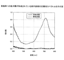
図7から、発色状態の表示層33は、720nm付近にシャープな吸収ピークを有することが確認された。
From FIG. 7, it was confirmed that the
(実施例2)
[エレクトロクロミック化合物(10)の合成]
化合物(B)0.45g、適量の臭化エチル、1−プロパノール3ml及び水6mlを反応フラスコに仕込み、90℃で40時間撹拌した後、放冷した。反応液を、水15mlと酢酸エチル30mlの混合液中に排出し、水層を分取した。得られた水層及び濃塩酸20mlを反応フラスコに仕込み、90℃で23時間撹拌した後、放冷した。反応液から水を留去し、タール状の残留物をメタノールに溶解させた後、撹拌下、2−プロパノール/エタノール混合溶媒(容量比2/1)中に滴下して生成物を結晶化させた。さらに、濾過した後、2−プロパノールで洗浄し、乾燥して、エレクトロクロミック化合物(10)0.30gを得た。
(Example 2)
[Synthesis of Electrochromic Compound (10)]
0.45 g of compound (B), an appropriate amount of ethyl bromide, 3 ml of 1-propanol and 6 ml of water were charged into a reaction flask, stirred at 90 ° C. for 40 hours, and then allowed to cool. The reaction solution was discharged into a mixed solution of 15 ml of water and 30 ml of ethyl acetate, and the aqueous layer was separated. The obtained aqueous layer and 20 ml of concentrated hydrochloric acid were charged into a reaction flask, stirred at 90 ° C. for 23 hours, and then allowed to cool. Water was distilled off from the reaction solution, and the tar-like residue was dissolved in methanol, and then dropped into a 2-propanol / ethanol mixed solvent (
[表示素子の作製]
表示基板11及び対向基板12として、上面の全面に、それぞれSnO2からなる表示電極11a及び対向電極12aが形成されている30mm×30mmのガラス基板11b及び12b(AGCファブリテック社製)を用いた。表示電極11aの端部間の抵抗を測定したところ、約20Ωであった。
[Production of display element]
As the
表示基板11及び対向基板12を、75μmのスペーサ15を介して貼り合わせ、セルを得た。次に、エレクトロクロミック化合物(10)13bの1質量%水/2,2,3,3−テトラフルオロプロパノール混合溶媒(質量比1/9)溶液を、過塩素酸テトラブチルアンモニウムを、ジメチルスルホキシド(DMSO)に対して、20質量%溶解させた液に対して、50質量%添加した電解液13aをセル内に封入して、白色反射層14が形成されていない形態の表示素子10を得た。
The
[発消色試験]
表示素子10の表示電極11aに負極を、対向電極12aに正極を接続し、3.0Vの電圧を2秒間印加したところ、シアンを発色した。次に、−3.0Vの電圧を4秒間印加したところ、完全に消色し、無色透明に戻った。また、表示素子10は、3.0Vの電圧を2秒間印加した後、電圧を印加せずに300秒間放置しても、発色状態が保持されたことから、画像保持特性に優れることが確認された。
[Color development test]
When a negative electrode was connected to the
(実施例3)
[エレクトロクロミック化合物(11)の合成]
2−ブロモエチルホスホン酸ジエチルの代わりに、4−(ブロモメチル)ベンジルホスホン酸ジエチルを用いた以外は、エレクトロクロミック化合物(2)と同様にして、エレクトロクロミック化合物(11)を得た。
(Example 3)
[Synthesis of Electrochromic Compound (11)]
An electrochromic compound (11) was obtained in the same manner as the electrochromic compound (2) except that diethyl 4- (bromomethyl) benzylphosphonate was used instead of diethyl 2-bromoethylphosphonate.
[表示素子の作製]
エレクトロクロミック化合物(2)の1質量%2,2,3,3−テトラフルオロプロパノール溶液の代わりに、エレクトロクロミック化合物(11)の1.5質量%2,2,3,3−テトラフルオロプロパノール溶液を用いた以外は、実施例1と同様にして、表示素子30を得た。
[Production of display element]
Instead of the 1
[発消色試験]
表示素子30の表示電極11aに負極を、対向電極12aに正極を接続し、3.0Vの電圧を0.5秒間印加したところ、シアンを発色した。次に、−4.5Vの電圧を2秒間印加したところ、完全に消色し、白色に戻った。また、表示素子30は、3.0Vの電圧を0.5秒間印加した後、電圧を印加せずに300秒間放置しても、発色状態が保持されたことから、画像保持特性に優れることが確認された。
[Color development test]
When a negative electrode was connected to the
(実施例4)
[表示素子の作製]
表示基板として、上面の全面にSnO2からなる表示電極11aが形成されている30mm×30mmのガラス基板11b(AGCファブリテック社製)を用いた。
Example 4
[Production of display element]
As the display substrate, a 30 mm × 30
次に、スピンコート法を用いて、表示電極11a上に、酸化チタンのナノ粒子の分散液SP210(昭和タイタニウム社製)を塗布し、120℃で15分間アニール処理して、ナノ粒子集積体を形成した。ナノ粒子集積体が形成された表示基板11を、3−ブロモプロピルトリクロロシランの0.02質量%トルエン溶液中に30分間浸漬し、ナノ粒子集積体を表面処理した。さらに、表面処理されたナノ粒子集積体が形成された表示基板11を、化合物(B)の0.1質量%トルエン溶液に浸漬し、2時間還流して、ナノ粒子集積体を表面処理して、エレクトロクロミック組成物33bを含む表示層33を形成した。
Next, a dispersion liquid SP210 of titanium oxide nanoparticles (manufactured by Showa Titanium Co., Ltd.) is applied onto the
一方、スパッタ法を用いて、30mm×30mmのガラス基板12bの上面の全面に、厚さが約150nmのITO膜を形成した。次に、スピンコート法を用いて、ITO膜上に、熱硬化性の導電性カーボンインクCH10(十条ケミカル社製)に対して、酢酸2−エトキシエチルを25質量%添加した液を塗布した後、120℃で15分間アニール処理して、対向電極12aを形成し、対向基板12を得た。
On the other hand, an ITO film having a thickness of about 150 nm was formed on the entire upper surface of the 30 mm × 30
表示基板11及び対向基板12を、75μmのスペーサ15を介して貼り合わせ、セルを得た。次に、過塩素酸テトラブチルアンモニウムを、ジメチルスルホキシド(DMSO)に対して、20質量%溶解させた電解液13a中に、平均一次粒径が300nmの酸化チタン粒子(石原産業社製)を35質量%分散させた液をセル内に封入して、白色反射層14を形成し、表示素子30を得た。
The
[発消色試験]
表示素子10の表示電極11aに負極を、対向電極12aに正極を接続し、3.0Vの電圧を1秒間印加したところ、シアンを発色した。次に、−4.5Vの電圧を2秒間印加したところ、完全に消色し、無色透明に戻った。また、表示素子10は、3.0Vの電圧を1秒間印加した後、電圧を印加せずに300秒間放置しても、発色状態が保持されたことから、画像保持特性に優れることが確認された。
[Color development test]
When a negative electrode was connected to the
(比較例1)
[表示素子の作製]
エレクトロクロミック化合物(2)の代わりに、化学式
(Comparative Example 1)
[Production of display element]
Instead of the electrochromic compound (2), the chemical formula
[発消色試験]
表示素子30の表示電極11aに負極を、対向電極12aに正極を接続し、3.0Vの電圧を1秒間印加したところ、青色を発色した。次に、−4.5Vの電圧を2秒間印加したところ、完全に消色し、白色に戻った。また、表示素子30は、3.0Vの電圧を1秒間印加した後、電圧を印加せずに300秒間放置しても、発色状態が保持されたことから、画像保持特性に優れることが確認された。
[Color development test]
When a negative electrode was connected to the
分光測色計LCD−5000(大塚電子社製)を用いて、発色状態の表示素子30に拡散光を照射したところ、図8に示す反射スペクトルが得られた。図8から、表示素子30は、可視域において反射率が低い領域の幅が広く、光吸収がブロードであるため、青色を発色することが確認された。
When the
10、20、30 表示素子
11 表示基板
11a 表示電極
11b 透明基板
12 対向基板
12a 対向電極
12b 基板
13、23 表示層
13a 電解液
13b エレクトロクロミック化合物
14 白色反射層
15 スペーサ
33 表示層
33b エレクトロクロミック組成物
DESCRIPTION OF
Claims (6)
で表されることを特徴とするエレクトロクロミック化合物。 General formula
An electrochromic compound represented by the formula:
で表される化合物を反応させた後、一般式
で表される化合物を反応させることにより得られることを特徴とするエレクトロクロミック組成物。 Structures with conductive or semiconducting nanoscale irregularities have a general formula
After reacting the compound represented by general formula
An electrochromic composition obtained by reacting a compound represented by the formula:
前記表示電極の前記対向電極側の表面に、請求項1若しくは2に記載のエレクトロクロミック化合物又は請求項3若しくは4に記載のエレクトロクロミック組成物を含む表示層が形成されていることを特徴とする表示素子。 A display element comprising: a display electrode; a counter electrode provided to face the display electrode at a predetermined interval; and an electrolyte sandwiched between the display electrode and the counter electrode. ,
A display layer containing the electrochromic compound according to claim 1 or 2 or the electrochromic composition according to claim 3 or 4 is formed on a surface of the display electrode on the counter electrode side. Display element.
前記表示素子を駆動する手段を有することを特徴とする表示装置。 A display element according to claim 5;
A display device comprising means for driving the display element.
Priority Applications (7)
| Application Number | Priority Date | Filing Date | Title |
|---|---|---|---|
| JP2010172866A JP5725397B2 (en) | 2009-10-16 | 2010-07-30 | Electrochromic compound |
| US13/501,007 US8593715B2 (en) | 2009-10-16 | 2010-10-08 | Electrochromic compound, electrochromic composition, and display element |
| CN201080057605.4A CN102666778B (en) | 2009-10-16 | 2010-10-08 | Electrochromic compounds, electrochromic compositions and display element |
| PCT/JP2010/068220 WO2011046222A1 (en) | 2009-10-16 | 2010-10-08 | Electrochromic compound, electrochromic composition, and display element |
| KR1020127009484A KR20120068911A (en) | 2009-10-16 | 2010-10-08 | Electrochromic compound, electrochromic composition, and display element |
| EP10823490.7A EP2488601B1 (en) | 2009-10-16 | 2010-10-08 | Electrochromic compound, electrochromic composition, and display element |
| TW099134894A TWI455935B (en) | 2009-10-16 | 2010-10-13 | Electrochromic compound, electrochromic composition, and display element |
Applications Claiming Priority (3)
| Application Number | Priority Date | Filing Date | Title |
|---|---|---|---|
| JP2009239891 | 2009-10-16 | ||
| JP2009239891 | 2009-10-16 | ||
| JP2010172866A JP5725397B2 (en) | 2009-10-16 | 2010-07-30 | Electrochromic compound |
Publications (2)
| Publication Number | Publication Date |
|---|---|
| JP2011102288A JP2011102288A (en) | 2011-05-26 |
| JP5725397B2 true JP5725397B2 (en) | 2015-05-27 |
Family
ID=44192797
Family Applications (1)
| Application Number | Title | Priority Date | Filing Date |
|---|---|---|---|
| JP2010172866A Expired - Fee Related JP5725397B2 (en) | 2009-10-16 | 2010-07-30 | Electrochromic compound |
Country Status (1)
| Country | Link |
|---|---|
| JP (1) | JP5725397B2 (en) |
Families Citing this family (2)
| Publication number | Priority date | Publication date | Assignee | Title |
|---|---|---|---|---|
| JP5790403B2 (en) | 2010-12-07 | 2015-10-07 | 株式会社リコー | Electrochromic display device |
| JP2013250520A (en) * | 2012-06-04 | 2013-12-12 | Ricoh Co Ltd | Electrochromic compound, electrochromic composition, and display element |
Family Cites Families (5)
| Publication number | Priority date | Publication date | Assignee | Title |
|---|---|---|---|---|
| JPS5918686B2 (en) * | 1973-09-21 | 1984-04-28 | 松下電器産業株式会社 | color display device |
| DE10001031A1 (en) * | 2000-01-13 | 2001-07-19 | Bayer Ag | Electrochromic device |
| JP4929995B2 (en) * | 2006-02-09 | 2012-05-09 | ソニー株式会社 | Electrochromic device |
| JP5648994B2 (en) * | 2009-10-16 | 2015-01-07 | 株式会社リコー | Electrochromic compound |
| JP5550094B2 (en) * | 2009-10-16 | 2014-07-16 | 株式会社リコー | Electrochromic compound, electrochromic composition, and display element |
-
2010
- 2010-07-30 JP JP2010172866A patent/JP5725397B2/en not_active Expired - Fee Related
Also Published As
| Publication number | Publication date |
|---|---|
| JP2011102288A (en) | 2011-05-26 |
Similar Documents
| Publication | Publication Date | Title |
|---|---|---|
| US11053267B2 (en) | Electrochromic compound, electrochromic composition, and display element | |
| JP5648994B2 (en) | Electrochromic compound | |
| JP6085914B2 (en) | Electrochromic compound, electrochromic composition, and display element | |
| JP5550094B2 (en) | Electrochromic compound, electrochromic composition, and display element | |
| JP2014159385A (en) | Electrochromic compound, electrochromic composition, and display element | |
| JP5900813B2 (en) | Electrochromic compound, electrochromic composition, and display element | |
| JP6399535B2 (en) | Electrochromic compound, electrochromic composition, display device using the same, and light control device | |
| JP2012224548A (en) | Electrochromic compound | |
| JP6213080B2 (en) | Electrochromic material, electrochromic composition, and electrochromic display element | |
| JP5725397B2 (en) | Electrochromic compound | |
| JP5617597B2 (en) | Electrochromic compound, electrochromic composition, and display element | |
| JP5949012B2 (en) | Electrochromic compound, electrochromic composition, and display element | |
| JP5811808B2 (en) | Electrochromic compound, electrochromic composition, and display element | |
| JP6519101B2 (en) | Electrochromic compound, electrochromic composition, display device and light control device | |
| JP5568858B2 (en) | Electrochromic composition and display element | |
| JP5962208B2 (en) | Electrochromic compound, electrochromic composition, and display element | |
| JP5939034B2 (en) | Electrochromic compound, electrochromic composition, and display element | |
| JP5875036B2 (en) | Electrochromic compound | |
| JP5880809B2 (en) | Electrochromic compound, electrochromic structure, and display element | |
| JP6387673B2 (en) | Electrochromic compound, electrochromic composition, display device and light control device | |
| JP2013250522A (en) | Electrochromic compound, electrochromic composition, and display element | |
| JP2013250520A (en) | Electrochromic compound, electrochromic composition, and display element |
Legal Events
| Date | Code | Title | Description |
|---|---|---|---|
| A621 | Written request for application examination |
Free format text: JAPANESE INTERMEDIATE CODE: A621 Effective date: 20130425 |
|
| A521 | Request for written amendment filed |
Free format text: JAPANESE INTERMEDIATE CODE: A821 Effective date: 20130425 |
|
| A521 | Request for written amendment filed |
Free format text: JAPANESE INTERMEDIATE CODE: A523 Effective date: 20130704 |
|
| A131 | Notification of reasons for refusal |
Free format text: JAPANESE INTERMEDIATE CODE: A131 Effective date: 20140819 |
|
| A521 | Request for written amendment filed |
Free format text: JAPANESE INTERMEDIATE CODE: A523 Effective date: 20141016 |
|
| TRDD | Decision of grant or rejection written | ||
| A01 | Written decision to grant a patent or to grant a registration (utility model) |
Free format text: JAPANESE INTERMEDIATE CODE: A01 Effective date: 20150224 |
|
| A61 | First payment of annual fees (during grant procedure) |
Free format text: JAPANESE INTERMEDIATE CODE: A61 Effective date: 20150319 |
|
| R150 | Certificate of patent or registration of utility model |
Ref document number: 5725397 Country of ref document: JP Free format text: JAPANESE INTERMEDIATE CODE: R150 |
|
| R250 | Receipt of annual fees |
Free format text: JAPANESE INTERMEDIATE CODE: R250 |
|
| R250 | Receipt of annual fees |
Free format text: JAPANESE INTERMEDIATE CODE: R250 |
|
| R250 | Receipt of annual fees |
Free format text: JAPANESE INTERMEDIATE CODE: R250 |
|
| R250 | Receipt of annual fees |
Free format text: JAPANESE INTERMEDIATE CODE: R250 |
|
| LAPS | Cancellation because of no payment of annual fees |