JP5717724B2 - Band gap adjustment of solar cells from liquid silane by addition of germanium - Google Patents
Band gap adjustment of solar cells from liquid silane by addition of germanium Download PDFInfo
- Publication number
- JP5717724B2 JP5717724B2 JP2012507719A JP2012507719A JP5717724B2 JP 5717724 B2 JP5717724 B2 JP 5717724B2 JP 2012507719 A JP2012507719 A JP 2012507719A JP 2012507719 A JP2012507719 A JP 2012507719A JP 5717724 B2 JP5717724 B2 JP 5717724B2
- Authority
- JP
- Japan
- Prior art keywords
- germanium
- silicon
- compound
- layer
- coating
- Prior art date
- Legal status (The legal status is an assumption and is not a legal conclusion. Google has not performed a legal analysis and makes no representation as to the accuracy of the status listed.)
- Expired - Fee Related
Links
- 229910052732 germanium Inorganic materials 0.000 title claims description 34
- GNPVGFCGXDBREM-UHFFFAOYSA-N germanium atom Chemical compound [Ge] GNPVGFCGXDBREM-UHFFFAOYSA-N 0.000 title claims description 34
- BLRPTPMANUNPDV-UHFFFAOYSA-N Silane Chemical compound [SiH4] BLRPTPMANUNPDV-UHFFFAOYSA-N 0.000 title claims description 8
- 229910000077 silane Inorganic materials 0.000 title claims description 8
- 239000007788 liquid Substances 0.000 title claims description 7
- 239000000203 mixture Substances 0.000 claims description 70
- 238000000034 method Methods 0.000 claims description 69
- 229910052710 silicon Inorganic materials 0.000 claims description 47
- 239000010703 silicon Substances 0.000 claims description 47
- XUIMIQQOPSSXEZ-UHFFFAOYSA-N Silicon Chemical compound [Si] XUIMIQQOPSSXEZ-UHFFFAOYSA-N 0.000 claims description 45
- 238000009472 formulation Methods 0.000 claims description 35
- 239000000758 substrate Substances 0.000 claims description 30
- 238000000576 coating method Methods 0.000 claims description 29
- 239000011248 coating agent Substances 0.000 claims description 28
- 150000002291 germanium compounds Chemical class 0.000 claims description 27
- 229910000577 Silicon-germanium Inorganic materials 0.000 claims description 21
- LEVVHYCKPQWKOP-UHFFFAOYSA-N [Si].[Ge] Chemical compound [Si].[Ge] LEVVHYCKPQWKOP-UHFFFAOYSA-N 0.000 claims description 21
- 238000004519 manufacturing process Methods 0.000 claims description 20
- 150000001875 compounds Chemical class 0.000 claims description 18
- 150000003377 silicon compounds Chemical group 0.000 claims description 16
- 238000006384 oligomerization reaction Methods 0.000 claims description 15
- 238000010438 heat treatment Methods 0.000 claims description 13
- 239000002019 doping agent Substances 0.000 claims description 12
- 230000008021 deposition Effects 0.000 claims description 8
- -1 silicon halide Chemical class 0.000 claims description 8
- 239000002904 solvent Substances 0.000 claims description 8
- 239000001257 hydrogen Substances 0.000 claims description 7
- 229910052739 hydrogen Inorganic materials 0.000 claims description 7
- 229910052736 halogen Inorganic materials 0.000 claims description 6
- 150000002367 halogens Chemical class 0.000 claims description 6
- 125000001190 organyl group Chemical group 0.000 claims description 6
- 150000002431 hydrogen Chemical class 0.000 claims description 5
- 229910000078 germane Inorganic materials 0.000 claims description 4
- 239000007791 liquid phase Substances 0.000 claims description 3
- 238000006116 polymerization reaction Methods 0.000 claims description 3
- 238000007606 doctor blade method Methods 0.000 claims description 2
- 238000005507 spraying Methods 0.000 claims description 2
- 230000005670 electromagnetic radiation Effects 0.000 claims 1
- YXFVVABEGXRONW-UHFFFAOYSA-N Toluene Chemical compound CC1=CC=CC=C1 YXFVVABEGXRONW-UHFFFAOYSA-N 0.000 description 30
- 230000000052 comparative effect Effects 0.000 description 28
- CVLHDNLPWKYNNR-UHFFFAOYSA-N pentasilolane Chemical compound [SiH2]1[SiH2][SiH2][SiH2][SiH2]1 CVLHDNLPWKYNNR-UHFFFAOYSA-N 0.000 description 18
- 238000005516 engineering process Methods 0.000 description 15
- 239000010408 film Substances 0.000 description 14
- 239000011261 inert gas Substances 0.000 description 12
- 239000010453 quartz Substances 0.000 description 12
- VYPSYNLAJGMNEJ-UHFFFAOYSA-N silicon dioxide Inorganic materials O=[Si]=O VYPSYNLAJGMNEJ-UHFFFAOYSA-N 0.000 description 12
- 150000004756 silanes Chemical class 0.000 description 10
- 238000000151 deposition Methods 0.000 description 7
- 238000010521 absorption reaction Methods 0.000 description 6
- 238000010790 dilution Methods 0.000 description 6
- 239000012895 dilution Substances 0.000 description 6
- 239000004065 semiconductor Substances 0.000 description 6
- 229920000642 polymer Polymers 0.000 description 5
- 239000000243 solution Substances 0.000 description 5
- 238000005227 gel permeation chromatography Methods 0.000 description 4
- 230000003287 optical effect Effects 0.000 description 4
- 229920000548 poly(silane) polymer Polymers 0.000 description 4
- COIOYMYWGDAQPM-UHFFFAOYSA-N tris(2-methylphenyl)phosphane Chemical compound CC1=CC=CC=C1P(C=1C(=CC=CC=1)C)C1=CC=CC=C1C COIOYMYWGDAQPM-UHFFFAOYSA-N 0.000 description 4
- 238000009281 ultraviolet germicidal irradiation Methods 0.000 description 4
- OKTJSMMVPCPJKN-UHFFFAOYSA-N Carbon Chemical compound [C] OKTJSMMVPCPJKN-UHFFFAOYSA-N 0.000 description 3
- 229910045601 alloy Inorganic materials 0.000 description 3
- 239000000956 alloy Substances 0.000 description 3
- 150000001639 boron compounds Chemical class 0.000 description 3
- 239000007789 gas Substances 0.000 description 3
- 239000000178 monomer Substances 0.000 description 3
- 229910052698 phosphorus Inorganic materials 0.000 description 3
- 239000011574 phosphorus Substances 0.000 description 3
- 238000000623 plasma-assisted chemical vapour deposition Methods 0.000 description 3
- 239000000126 substance Substances 0.000 description 3
- XKRFYHLGVUSROY-UHFFFAOYSA-N Argon Chemical compound [Ar] XKRFYHLGVUSROY-UHFFFAOYSA-N 0.000 description 2
- IJGRMHOSHXDMSA-UHFFFAOYSA-N Atomic nitrogen Chemical compound N#N IJGRMHOSHXDMSA-UHFFFAOYSA-N 0.000 description 2
- UFHFLCQGNIYNRP-UHFFFAOYSA-N Hydrogen Chemical compound [H][H] UFHFLCQGNIYNRP-UHFFFAOYSA-N 0.000 description 2
- 239000004793 Polystyrene Substances 0.000 description 2
- 239000012300 argon atmosphere Substances 0.000 description 2
- 238000011088 calibration curve Methods 0.000 description 2
- 229910052799 carbon Inorganic materials 0.000 description 2
- DIOQZVSQGTUSAI-UHFFFAOYSA-N decane Chemical compound CCCCCCCCCC DIOQZVSQGTUSAI-UHFFFAOYSA-N 0.000 description 2
- 238000009826 distribution Methods 0.000 description 2
- 230000000694 effects Effects 0.000 description 2
- 239000012212 insulator Substances 0.000 description 2
- 238000005259 measurement Methods 0.000 description 2
- 229910052751 metal Inorganic materials 0.000 description 2
- 239000002184 metal Substances 0.000 description 2
- BKIMMITUMNQMOS-UHFFFAOYSA-N nonane Chemical compound CCCCCCCCC BKIMMITUMNQMOS-UHFFFAOYSA-N 0.000 description 2
- 229920002223 polystyrene Polymers 0.000 description 2
- 230000003595 spectral effect Effects 0.000 description 2
- 239000010409 thin film Substances 0.000 description 2
- XDTMQSROBMDMFD-UHFFFAOYSA-N Cyclohexane Chemical compound C1CCCCC1 XDTMQSROBMDMFD-UHFFFAOYSA-N 0.000 description 1
- CTQNGGLPUBDAKN-UHFFFAOYSA-N O-Xylene Chemical compound CC1=CC=CC=C1C CTQNGGLPUBDAKN-UHFFFAOYSA-N 0.000 description 1
- 238000002835 absorbance Methods 0.000 description 1
- 150000001338 aliphatic hydrocarbons Chemical class 0.000 description 1
- 229910052783 alkali metal Inorganic materials 0.000 description 1
- 150000001340 alkali metals Chemical class 0.000 description 1
- 238000000137 annealing Methods 0.000 description 1
- 229910052786 argon Inorganic materials 0.000 description 1
- 150000004945 aromatic hydrocarbons Chemical class 0.000 description 1
- LUXIMSHPDKSEDK-UHFFFAOYSA-N bis(disilanyl)silane Chemical compound [SiH3][SiH2][SiH2][SiH2][SiH3] LUXIMSHPDKSEDK-UHFFFAOYSA-N 0.000 description 1
- 238000005266 casting Methods 0.000 description 1
- 230000003197 catalytic effect Effects 0.000 description 1
- 239000000919 ceramic Substances 0.000 description 1
- 239000003795 chemical substances by application Substances 0.000 description 1
- 238000005229 chemical vapour deposition Methods 0.000 description 1
- 239000004020 conductor Substances 0.000 description 1
- 229920001577 copolymer Polymers 0.000 description 1
- 238000004132 cross linking Methods 0.000 description 1
- 239000013078 crystal Substances 0.000 description 1
- 229910021419 crystalline silicon Inorganic materials 0.000 description 1
- 150000004759 cyclic silanes Chemical class 0.000 description 1
- WJTCGQSWYFHTAC-UHFFFAOYSA-N cyclooctane Chemical compound C1CCCCCCC1 WJTCGQSWYFHTAC-UHFFFAOYSA-N 0.000 description 1
- 239000004914 cyclooctane Substances 0.000 description 1
- 230000007423 decrease Effects 0.000 description 1
- 230000001419 dependent effect Effects 0.000 description 1
- 238000001514 detection method Methods 0.000 description 1
- 238000009792 diffusion process Methods 0.000 description 1
- 239000011888 foil Substances 0.000 description 1
- 239000011521 glass Substances 0.000 description 1
- 239000010439 graphite Substances 0.000 description 1
- 229910002804 graphite Inorganic materials 0.000 description 1
- 150000004678 hydrides Chemical class 0.000 description 1
- 238000002513 implantation Methods 0.000 description 1
- 230000001678 irradiating effect Effects 0.000 description 1
- 239000012669 liquid formulation Substances 0.000 description 1
- 239000000463 material Substances 0.000 description 1
- 239000011159 matrix material Substances 0.000 description 1
- 230000008018 melting Effects 0.000 description 1
- 238000002844 melting Methods 0.000 description 1
- AUHZEENZYGFFBQ-UHFFFAOYSA-N mesitylene Substances CC1=CC(C)=CC(C)=C1 AUHZEENZYGFFBQ-UHFFFAOYSA-N 0.000 description 1
- 125000001827 mesitylenyl group Chemical group [H]C1=C(C(*)=C(C([H])=C1C([H])([H])[H])C([H])([H])[H])C([H])([H])[H] 0.000 description 1
- 229910001092 metal group alloy Inorganic materials 0.000 description 1
- 150000002739 metals Chemical class 0.000 description 1
- 230000004048 modification Effects 0.000 description 1
- 238000012986 modification Methods 0.000 description 1
- 229910021421 monocrystalline silicon Inorganic materials 0.000 description 1
- 229910052757 nitrogen Inorganic materials 0.000 description 1
- TVMXDCGIABBOFY-UHFFFAOYSA-N octane Chemical compound CCCCCCCC TVMXDCGIABBOFY-UHFFFAOYSA-N 0.000 description 1
- 239000012071 phase Substances 0.000 description 1
- 239000004033 plastic Substances 0.000 description 1
- 229920003023 plastic Polymers 0.000 description 1
- 229910021420 polycrystalline silicon Inorganic materials 0.000 description 1
- 239000002243 precursor Substances 0.000 description 1
- 238000002360 preparation method Methods 0.000 description 1
- 238000006862 quantum yield reaction Methods 0.000 description 1
- 239000011856 silicon-based particle Substances 0.000 description 1
- 238000003786 synthesis reaction Methods 0.000 description 1
- 235000012431 wafers Nutrition 0.000 description 1
- 239000008096 xylene Substances 0.000 description 1
Images

Classifications
-
- H—ELECTRICITY
- H01—ELECTRIC ELEMENTS
- H01L—SEMICONDUCTOR DEVICES NOT COVERED BY CLASS H10
- H01L31/00—Semiconductor devices sensitive to infrared radiation, light, electromagnetic radiation of shorter wavelength or corpuscular radiation and specially adapted either for the conversion of the energy of such radiation into electrical energy or for the control of electrical energy by such radiation; Processes or apparatus specially adapted for the manufacture or treatment thereof or of parts thereof; Details thereof
- H01L31/02—Details
- H01L31/0216—Coatings
-
- C—CHEMISTRY; METALLURGY
- C23—COATING METALLIC MATERIAL; COATING MATERIAL WITH METALLIC MATERIAL; CHEMICAL SURFACE TREATMENT; DIFFUSION TREATMENT OF METALLIC MATERIAL; COATING BY VACUUM EVAPORATION, BY SPUTTERING, BY ION IMPLANTATION OR BY CHEMICAL VAPOUR DEPOSITION, IN GENERAL; INHIBITING CORROSION OF METALLIC MATERIAL OR INCRUSTATION IN GENERAL
- C23C—COATING METALLIC MATERIAL; COATING MATERIAL WITH METALLIC MATERIAL; SURFACE TREATMENT OF METALLIC MATERIAL BY DIFFUSION INTO THE SURFACE, BY CHEMICAL CONVERSION OR SUBSTITUTION; COATING BY VACUUM EVAPORATION, BY SPUTTERING, BY ION IMPLANTATION OR BY CHEMICAL VAPOUR DEPOSITION, IN GENERAL
- C23C18/00—Chemical coating by decomposition of either liquid compounds or solutions of the coating forming compounds, without leaving reaction products of surface material in the coating; Contact plating
- C23C18/02—Chemical coating by decomposition of either liquid compounds or solutions of the coating forming compounds, without leaving reaction products of surface material in the coating; Contact plating by thermal decomposition
- C23C18/12—Chemical coating by decomposition of either liquid compounds or solutions of the coating forming compounds, without leaving reaction products of surface material in the coating; Contact plating by thermal decomposition characterised by the deposition of inorganic material other than metallic material
- C23C18/125—Process of deposition of the inorganic material
- C23C18/1295—Process of deposition of the inorganic material with after-treatment of the deposited inorganic material
-
- C—CHEMISTRY; METALLURGY
- C23—COATING METALLIC MATERIAL; COATING MATERIAL WITH METALLIC MATERIAL; CHEMICAL SURFACE TREATMENT; DIFFUSION TREATMENT OF METALLIC MATERIAL; COATING BY VACUUM EVAPORATION, BY SPUTTERING, BY ION IMPLANTATION OR BY CHEMICAL VAPOUR DEPOSITION, IN GENERAL; INHIBITING CORROSION OF METALLIC MATERIAL OR INCRUSTATION IN GENERAL
- C23C—COATING METALLIC MATERIAL; COATING MATERIAL WITH METALLIC MATERIAL; SURFACE TREATMENT OF METALLIC MATERIAL BY DIFFUSION INTO THE SURFACE, BY CHEMICAL CONVERSION OR SUBSTITUTION; COATING BY VACUUM EVAPORATION, BY SPUTTERING, BY ION IMPLANTATION OR BY CHEMICAL VAPOUR DEPOSITION, IN GENERAL
- C23C18/00—Chemical coating by decomposition of either liquid compounds or solutions of the coating forming compounds, without leaving reaction products of surface material in the coating; Contact plating
- C23C18/02—Chemical coating by decomposition of either liquid compounds or solutions of the coating forming compounds, without leaving reaction products of surface material in the coating; Contact plating by thermal decomposition
- C23C18/12—Chemical coating by decomposition of either liquid compounds or solutions of the coating forming compounds, without leaving reaction products of surface material in the coating; Contact plating by thermal decomposition characterised by the deposition of inorganic material other than metallic material
- C23C18/1204—Chemical coating by decomposition of either liquid compounds or solutions of the coating forming compounds, without leaving reaction products of surface material in the coating; Contact plating by thermal decomposition characterised by the deposition of inorganic material other than metallic material inorganic material, e.g. non-oxide and non-metallic such as sulfides, nitrides based compounds
- C23C18/122—Inorganic polymers, e.g. silanes, polysilazanes, polysiloxanes
-
- C—CHEMISTRY; METALLURGY
- C23—COATING METALLIC MATERIAL; COATING MATERIAL WITH METALLIC MATERIAL; CHEMICAL SURFACE TREATMENT; DIFFUSION TREATMENT OF METALLIC MATERIAL; COATING BY VACUUM EVAPORATION, BY SPUTTERING, BY ION IMPLANTATION OR BY CHEMICAL VAPOUR DEPOSITION, IN GENERAL; INHIBITING CORROSION OF METALLIC MATERIAL OR INCRUSTATION IN GENERAL
- C23C—COATING METALLIC MATERIAL; COATING MATERIAL WITH METALLIC MATERIAL; SURFACE TREATMENT OF METALLIC MATERIAL BY DIFFUSION INTO THE SURFACE, BY CHEMICAL CONVERSION OR SUBSTITUTION; COATING BY VACUUM EVAPORATION, BY SPUTTERING, BY ION IMPLANTATION OR BY CHEMICAL VAPOUR DEPOSITION, IN GENERAL
- C23C18/00—Chemical coating by decomposition of either liquid compounds or solutions of the coating forming compounds, without leaving reaction products of surface material in the coating; Contact plating
- C23C18/02—Chemical coating by decomposition of either liquid compounds or solutions of the coating forming compounds, without leaving reaction products of surface material in the coating; Contact plating by thermal decomposition
- C23C18/12—Chemical coating by decomposition of either liquid compounds or solutions of the coating forming compounds, without leaving reaction products of surface material in the coating; Contact plating by thermal decomposition characterised by the deposition of inorganic material other than metallic material
- C23C18/1229—Composition of the substrate
- C23C18/1245—Inorganic substrates other than metallic
-
- C—CHEMISTRY; METALLURGY
- C23—COATING METALLIC MATERIAL; COATING MATERIAL WITH METALLIC MATERIAL; CHEMICAL SURFACE TREATMENT; DIFFUSION TREATMENT OF METALLIC MATERIAL; COATING BY VACUUM EVAPORATION, BY SPUTTERING, BY ION IMPLANTATION OR BY CHEMICAL VAPOUR DEPOSITION, IN GENERAL; INHIBITING CORROSION OF METALLIC MATERIAL OR INCRUSTATION IN GENERAL
- C23C—COATING METALLIC MATERIAL; COATING MATERIAL WITH METALLIC MATERIAL; SURFACE TREATMENT OF METALLIC MATERIAL BY DIFFUSION INTO THE SURFACE, BY CHEMICAL CONVERSION OR SUBSTITUTION; COATING BY VACUUM EVAPORATION, BY SPUTTERING, BY ION IMPLANTATION OR BY CHEMICAL VAPOUR DEPOSITION, IN GENERAL
- C23C18/00—Chemical coating by decomposition of either liquid compounds or solutions of the coating forming compounds, without leaving reaction products of surface material in the coating; Contact plating
- C23C18/14—Decomposition by irradiation, e.g. photolysis, particle radiation or by mixed irradiation sources
- C23C18/143—Radiation by light, e.g. photolysis or pyrolysis
-
- H—ELECTRICITY
- H01—ELECTRIC ELEMENTS
- H01L—SEMICONDUCTOR DEVICES NOT COVERED BY CLASS H10
- H01L21/00—Processes or apparatus adapted for the manufacture or treatment of semiconductor or solid state devices or of parts thereof
- H01L21/02—Manufacture or treatment of semiconductor devices or of parts thereof
- H01L21/02104—Forming layers
- H01L21/02365—Forming inorganic semiconducting materials on a substrate
- H01L21/02367—Substrates
- H01L21/0237—Materials
- H01L21/0242—Crystalline insulating materials
-
- H—ELECTRICITY
- H01—ELECTRIC ELEMENTS
- H01L—SEMICONDUCTOR DEVICES NOT COVERED BY CLASS H10
- H01L21/00—Processes or apparatus adapted for the manufacture or treatment of semiconductor or solid state devices or of parts thereof
- H01L21/02—Manufacture or treatment of semiconductor devices or of parts thereof
- H01L21/02104—Forming layers
- H01L21/02365—Forming inorganic semiconducting materials on a substrate
- H01L21/02518—Deposited layers
- H01L21/02521—Materials
- H01L21/02524—Group 14 semiconducting materials
- H01L21/02532—Silicon, silicon germanium, germanium
-
- H—ELECTRICITY
- H01—ELECTRIC ELEMENTS
- H01L—SEMICONDUCTOR DEVICES NOT COVERED BY CLASS H10
- H01L21/00—Processes or apparatus adapted for the manufacture or treatment of semiconductor or solid state devices or of parts thereof
- H01L21/02—Manufacture or treatment of semiconductor devices or of parts thereof
- H01L21/02104—Forming layers
- H01L21/02365—Forming inorganic semiconducting materials on a substrate
- H01L21/02612—Formation types
- H01L21/02617—Deposition types
- H01L21/02623—Liquid deposition
- H01L21/02628—Liquid deposition using solutions
-
- H—ELECTRICITY
- H01—ELECTRIC ELEMENTS
- H01L—SEMICONDUCTOR DEVICES NOT COVERED BY CLASS H10
- H01L31/00—Semiconductor devices sensitive to infrared radiation, light, electromagnetic radiation of shorter wavelength or corpuscular radiation and specially adapted either for the conversion of the energy of such radiation into electrical energy or for the control of electrical energy by such radiation; Processes or apparatus specially adapted for the manufacture or treatment thereof or of parts thereof; Details thereof
- H01L31/0248—Semiconductor devices sensitive to infrared radiation, light, electromagnetic radiation of shorter wavelength or corpuscular radiation and specially adapted either for the conversion of the energy of such radiation into electrical energy or for the control of electrical energy by such radiation; Processes or apparatus specially adapted for the manufacture or treatment thereof or of parts thereof; Details thereof characterised by their semiconductor bodies
- H01L31/0256—Semiconductor devices sensitive to infrared radiation, light, electromagnetic radiation of shorter wavelength or corpuscular radiation and specially adapted either for the conversion of the energy of such radiation into electrical energy or for the control of electrical energy by such radiation; Processes or apparatus specially adapted for the manufacture or treatment thereof or of parts thereof; Details thereof characterised by their semiconductor bodies characterised by the material
- H01L31/0264—Inorganic materials
- H01L31/028—Inorganic materials including, apart from doping material or other impurities, only elements of Group IV of the Periodic System
-
- H—ELECTRICITY
- H01—ELECTRIC ELEMENTS
- H01L—SEMICONDUCTOR DEVICES NOT COVERED BY CLASS H10
- H01L31/00—Semiconductor devices sensitive to infrared radiation, light, electromagnetic radiation of shorter wavelength or corpuscular radiation and specially adapted either for the conversion of the energy of such radiation into electrical energy or for the control of electrical energy by such radiation; Processes or apparatus specially adapted for the manufacture or treatment thereof or of parts thereof; Details thereof
- H01L31/0248—Semiconductor devices sensitive to infrared radiation, light, electromagnetic radiation of shorter wavelength or corpuscular radiation and specially adapted either for the conversion of the energy of such radiation into electrical energy or for the control of electrical energy by such radiation; Processes or apparatus specially adapted for the manufacture or treatment thereof or of parts thereof; Details thereof characterised by their semiconductor bodies
- H01L31/036—Semiconductor devices sensitive to infrared radiation, light, electromagnetic radiation of shorter wavelength or corpuscular radiation and specially adapted either for the conversion of the energy of such radiation into electrical energy or for the control of electrical energy by such radiation; Processes or apparatus specially adapted for the manufacture or treatment thereof or of parts thereof; Details thereof characterised by their semiconductor bodies characterised by their crystalline structure or particular orientation of the crystalline planes
- H01L31/0368—Semiconductor devices sensitive to infrared radiation, light, electromagnetic radiation of shorter wavelength or corpuscular radiation and specially adapted either for the conversion of the energy of such radiation into electrical energy or for the control of electrical energy by such radiation; Processes or apparatus specially adapted for the manufacture or treatment thereof or of parts thereof; Details thereof characterised by their semiconductor bodies characterised by their crystalline structure or particular orientation of the crystalline planes including polycrystalline semiconductors
- H01L31/03682—Semiconductor devices sensitive to infrared radiation, light, electromagnetic radiation of shorter wavelength or corpuscular radiation and specially adapted either for the conversion of the energy of such radiation into electrical energy or for the control of electrical energy by such radiation; Processes or apparatus specially adapted for the manufacture or treatment thereof or of parts thereof; Details thereof characterised by their semiconductor bodies characterised by their crystalline structure or particular orientation of the crystalline planes including polycrystalline semiconductors including only elements of Group IV of the Periodic System
- H01L31/03687—Semiconductor devices sensitive to infrared radiation, light, electromagnetic radiation of shorter wavelength or corpuscular radiation and specially adapted either for the conversion of the energy of such radiation into electrical energy or for the control of electrical energy by such radiation; Processes or apparatus specially adapted for the manufacture or treatment thereof or of parts thereof; Details thereof characterised by their semiconductor bodies characterised by their crystalline structure or particular orientation of the crystalline planes including polycrystalline semiconductors including only elements of Group IV of the Periodic System including microcrystalline AIVBIV alloys, e.g. uc-SiGe, uc-SiC
-
- H—ELECTRICITY
- H01—ELECTRIC ELEMENTS
- H01L—SEMICONDUCTOR DEVICES NOT COVERED BY CLASS H10
- H01L31/00—Semiconductor devices sensitive to infrared radiation, light, electromagnetic radiation of shorter wavelength or corpuscular radiation and specially adapted either for the conversion of the energy of such radiation into electrical energy or for the control of electrical energy by such radiation; Processes or apparatus specially adapted for the manufacture or treatment thereof or of parts thereof; Details thereof
- H01L31/0248—Semiconductor devices sensitive to infrared radiation, light, electromagnetic radiation of shorter wavelength or corpuscular radiation and specially adapted either for the conversion of the energy of such radiation into electrical energy or for the control of electrical energy by such radiation; Processes or apparatus specially adapted for the manufacture or treatment thereof or of parts thereof; Details thereof characterised by their semiconductor bodies
- H01L31/036—Semiconductor devices sensitive to infrared radiation, light, electromagnetic radiation of shorter wavelength or corpuscular radiation and specially adapted either for the conversion of the energy of such radiation into electrical energy or for the control of electrical energy by such radiation; Processes or apparatus specially adapted for the manufacture or treatment thereof or of parts thereof; Details thereof characterised by their semiconductor bodies characterised by their crystalline structure or particular orientation of the crystalline planes
- H01L31/0392—Semiconductor devices sensitive to infrared radiation, light, electromagnetic radiation of shorter wavelength or corpuscular radiation and specially adapted either for the conversion of the energy of such radiation into electrical energy or for the control of electrical energy by such radiation; Processes or apparatus specially adapted for the manufacture or treatment thereof or of parts thereof; Details thereof characterised by their semiconductor bodies characterised by their crystalline structure or particular orientation of the crystalline planes including thin films deposited on metallic or insulating substrates ; characterised by specific substrate materials or substrate features or by the presence of intermediate layers, e.g. barrier layers, on the substrate
-
- H—ELECTRICITY
- H01—ELECTRIC ELEMENTS
- H01L—SEMICONDUCTOR DEVICES NOT COVERED BY CLASS H10
- H01L31/00—Semiconductor devices sensitive to infrared radiation, light, electromagnetic radiation of shorter wavelength or corpuscular radiation and specially adapted either for the conversion of the energy of such radiation into electrical energy or for the control of electrical energy by such radiation; Processes or apparatus specially adapted for the manufacture or treatment thereof or of parts thereof; Details thereof
- H01L31/18—Processes or apparatus specially adapted for the manufacture or treatment of these devices or of parts thereof
- H01L31/1804—Processes or apparatus specially adapted for the manufacture or treatment of these devices or of parts thereof comprising only elements of Group IV of the Periodic System
- H01L31/1812—Processes or apparatus specially adapted for the manufacture or treatment of these devices or of parts thereof comprising only elements of Group IV of the Periodic System including only AIVBIV alloys, e.g. SiGe
- H01L31/1816—Special manufacturing methods for microcrystalline layers, e.g. uc-SiGe, uc-SiC
-
- H—ELECTRICITY
- H01—ELECTRIC ELEMENTS
- H01L—SEMICONDUCTOR DEVICES NOT COVERED BY CLASS H10
- H01L31/00—Semiconductor devices sensitive to infrared radiation, light, electromagnetic radiation of shorter wavelength or corpuscular radiation and specially adapted either for the conversion of the energy of such radiation into electrical energy or for the control of electrical energy by such radiation; Processes or apparatus specially adapted for the manufacture or treatment thereof or of parts thereof; Details thereof
- H01L31/18—Processes or apparatus specially adapted for the manufacture or treatment of these devices or of parts thereof
- H01L31/186—Particular post-treatment for the devices, e.g. annealing, impurity gettering, short-circuit elimination, recrystallisation
- H01L31/1864—Annealing
-
- H—ELECTRICITY
- H01—ELECTRIC ELEMENTS
- H01L—SEMICONDUCTOR DEVICES NOT COVERED BY CLASS H10
- H01L31/00—Semiconductor devices sensitive to infrared radiation, light, electromagnetic radiation of shorter wavelength or corpuscular radiation and specially adapted either for the conversion of the energy of such radiation into electrical energy or for the control of electrical energy by such radiation; Processes or apparatus specially adapted for the manufacture or treatment thereof or of parts thereof; Details thereof
- H01L31/18—Processes or apparatus specially adapted for the manufacture or treatment of these devices or of parts thereof
- H01L31/20—Processes or apparatus specially adapted for the manufacture or treatment of these devices or of parts thereof such devices or parts thereof comprising amorphous semiconductor materials
- H01L31/202—Processes or apparatus specially adapted for the manufacture or treatment of these devices or of parts thereof such devices or parts thereof comprising amorphous semiconductor materials including only elements of Group IV of the Periodic System
- H01L31/204—Processes or apparatus specially adapted for the manufacture or treatment of these devices or of parts thereof such devices or parts thereof comprising amorphous semiconductor materials including only elements of Group IV of the Periodic System including AIVBIV alloys, e.g. SiGe, SiC
-
- Y—GENERAL TAGGING OF NEW TECHNOLOGICAL DEVELOPMENTS; GENERAL TAGGING OF CROSS-SECTIONAL TECHNOLOGIES SPANNING OVER SEVERAL SECTIONS OF THE IPC; TECHNICAL SUBJECTS COVERED BY FORMER USPC CROSS-REFERENCE ART COLLECTIONS [XRACs] AND DIGESTS
- Y02—TECHNOLOGIES OR APPLICATIONS FOR MITIGATION OR ADAPTATION AGAINST CLIMATE CHANGE
- Y02E—REDUCTION OF GREENHOUSE GAS [GHG] EMISSIONS, RELATED TO ENERGY GENERATION, TRANSMISSION OR DISTRIBUTION
- Y02E10/00—Energy generation through renewable energy sources
- Y02E10/50—Photovoltaic [PV] energy
- Y02E10/547—Monocrystalline silicon PV cells
-
- Y—GENERAL TAGGING OF NEW TECHNOLOGICAL DEVELOPMENTS; GENERAL TAGGING OF CROSS-SECTIONAL TECHNOLOGIES SPANNING OVER SEVERAL SECTIONS OF THE IPC; TECHNICAL SUBJECTS COVERED BY FORMER USPC CROSS-REFERENCE ART COLLECTIONS [XRACs] AND DIGESTS
- Y02—TECHNOLOGIES OR APPLICATIONS FOR MITIGATION OR ADAPTATION AGAINST CLIMATE CHANGE
- Y02E—REDUCTION OF GREENHOUSE GAS [GHG] EMISSIONS, RELATED TO ENERGY GENERATION, TRANSMISSION OR DISTRIBUTION
- Y02E10/00—Energy generation through renewable energy sources
- Y02E10/50—Photovoltaic [PV] energy
- Y02E10/548—Amorphous silicon PV cells
-
- Y—GENERAL TAGGING OF NEW TECHNOLOGICAL DEVELOPMENTS; GENERAL TAGGING OF CROSS-SECTIONAL TECHNOLOGIES SPANNING OVER SEVERAL SECTIONS OF THE IPC; TECHNICAL SUBJECTS COVERED BY FORMER USPC CROSS-REFERENCE ART COLLECTIONS [XRACs] AND DIGESTS
- Y02—TECHNOLOGIES OR APPLICATIONS FOR MITIGATION OR ADAPTATION AGAINST CLIMATE CHANGE
- Y02P—CLIMATE CHANGE MITIGATION TECHNOLOGIES IN THE PRODUCTION OR PROCESSING OF GOODS
- Y02P70/00—Climate change mitigation technologies in the production process for final industrial or consumer products
- Y02P70/50—Manufacturing or production processes characterised by the final manufactured product
-
- Y—GENERAL TAGGING OF NEW TECHNOLOGICAL DEVELOPMENTS; GENERAL TAGGING OF CROSS-SECTIONAL TECHNOLOGIES SPANNING OVER SEVERAL SECTIONS OF THE IPC; TECHNICAL SUBJECTS COVERED BY FORMER USPC CROSS-REFERENCE ART COLLECTIONS [XRACs] AND DIGESTS
- Y10—TECHNICAL SUBJECTS COVERED BY FORMER USPC
- Y10T—TECHNICAL SUBJECTS COVERED BY FORMER US CLASSIFICATION
- Y10T428/00—Stock material or miscellaneous articles
- Y10T428/31504—Composite [nonstructural laminate]
- Y10T428/31652—Of asbestos
- Y10T428/31663—As siloxane, silicone or silane
Description
本発明は、シリコン化合物含有配合物による基板のコーティングを用いた光起電素子の製造の際の、例えば液体シラン配合物で基板をコーティングする段階を含む太陽電池製造の際の、バンドギャップ(Bandluecke)シフトの減少またはなくす方法に関する。本発明は、かかる光起電素子の製造方法にも関する。 The present invention relates to a band gap (Bandluecke) in the manufacture of photovoltaic devices using a coating of a substrate with a silicon compound-containing formulation, for example in the production of solar cells comprising the step of coating the substrate with a liquid silane formulation. ) Relates to a method of reducing or eliminating shifts. The invention also relates to a method for producing such a photovoltaic element.
太陽電池の従来の製造は、打ち込みまたは拡散を用いて、ドープされた半導体基板のカウンタードープ、或いはエピタキシャル法を用いてドープされた半導体基板上でのカウンタードープされた半導体層の堆積において、または、真空中での気相による、または上記の方法の変形による種々のドーピングの半導体層の堆積のいずれかで成り立っている。全てのこれらの方法の欠点は、運転に必要な経済上のおよび価格上の費用である。 Conventional fabrication of solar cells includes implantation or diffusion, counter-doping of a doped semiconductor substrate, or deposition of a counter-doped semiconductor layer on a semiconductor substrate doped using an epitaxial method, or It consists of the deposition of variously doped semiconductor layers, either by vapor in vacuum or by a modification of the above method. The disadvantage of all these methods is the economic and price costs required for operation.
必須の真空技術、高温および/または高価な基板を回避するために、液相のシランによる層または層連続物の製造が試されている。 In order to avoid the essential vacuum technology, high temperatures and / or expensive substrates, the production of layers or layer successions with liquid phase silanes has been tried.
適した基板上への、これらのシランの1層またはそれより多くの層の堆積によって、太陽電池としてはたらくp−n接合を生産できる。該堆積は、スピンコーターを用いて行われる。生じた層は、適した温度処理によって安定化させられることから、それは典型的には微結晶、ナノ結晶およびアモルファス(単に、多形)構造の混合物と想定される。明示されない場合は、ここで、全ての微結晶、ナノ結晶、および/またはアモルファス層は一般に「多形」として示されることとし、なぜなら、大抵の場合、正確な区別および定義はあまりうまくいかないか、もしくは得られた結果についてあまり意味をなさないからである。 The deposition of one or more layers of these silanes on a suitable substrate can produce a pn junction that acts as a solar cell. The deposition is performed using a spin coater. Since the resulting layer is stabilized by a suitable temperature treatment, it is typically assumed to be a mixture of microcrystalline, nanocrystalline and amorphous (simply polymorphic) structures. Where not explicitly stated here, all microcrystalline, nanocrystalline, and / or amorphous layers shall generally be indicated as “polymorphic”, because in most cases the exact distinction and definition will not work very well, or This is because the results obtained do not make much sense.
シランからどのようにシリコン層を製造するのかについては自体公知である。GB2077710号は、アルカリ金属を用いたSiH2Cl2の同時の還元および重合による、一般式−(SiH2)n− (n≧10)のポリシランの製造を教示している。かかるより高次シランは、例えば太陽電池用のシリコン層のための前駆体として挙げられる。nについてより低い値、即ちn≦4を有するシラン SinH2n+2の場合、JP7267621号は、かかるシランの膜によるシリコン層の製造を教示し、該シランを冷たい状態でUV照射し、その後、400℃を上回る温度に加熱する。さらに、EP1284306号は、一般式SinH2nの環状シランおよび一般式SinH2n+2の非環式シラン(それぞれn=3ないし10)から、同様に、シリコン膜を製造できることを教示している。その際、それらのシランは、例えば加熱および/またはUV照射によって、部分的または完全にオリゴマー化される。さらに、n型もしくはp型ドープを実現するために、特別なリン化合物もしくはホウ素化合物が添加される。 It is known per se how to produce a silicon layer from silane. GB 2077710 teaches the preparation of polysilanes of the general formula — (SiH 2 ) n — (n ≧ 10) by simultaneous reduction and polymerization of SiH 2 Cl 2 using alkali metals. Such higher order silanes are cited as precursors for silicon layers for solar cells, for example. In the case of silanes Si n H 2n + 2 with lower values for n, ie n ≦ 4, JP 7267621 teaches the production of a silicon layer with a film of such silanes, which is then UV irradiated in the cold state, after which , Heated to a temperature above 400 ° C. Further, No. EP1284306, from the general formula Si n H 2n of cyclic silane and the general formula Si n H 2n + 2 acyclic silanes (n = 3 to 10, respectively), teach that likewise can be produced silicon film ing. The silanes are then partially or fully oligomerized, for example by heating and / or UV irradiation. Furthermore, a special phosphorus compound or boron compound is added to realize n-type or p-type doping.
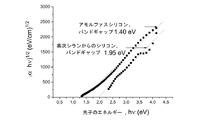
従来技術によって製造される薄膜は、青色シフト(blue shift)として示され且つ他の調べられた測定対象から公知である、光電特性を示す。特徴的な大きさ(当該の場合、シリコン粒子の直径)がナノメートル領域の値を有すると同時に、その光学パラメータを青色にシフトする。生じるシリコン層による光子の吸収は、まず、青色で始まる一方、日光の他のスペクトル領域での吸収は、従来の単結晶シリコンについてよりも著しく低い。使用材料が1.1〜1.5eVのバンドギャップを有する場合、太陽電池が最大効率を有することが文献から公知である。バンドギャップを例えば1.95eVに高めることは、技術的には、1の太陽光採光(Sonne Beleuchtung)の際に達成可能な効率を約71%に、且つ、1000の太陽光集光器採光の際に57%に低下させることを意味する (Goetzberger,A. et al.: Crystalline Silicon Solar Cells, Wiley, New York, 186ページ (1994))。高められたバンドギャップ(アモルファスについての1.4eVから多形シリコンについての1.95eVにかけて)についての検出を、図1に示す。バンドギャップは、分光エリプソメータ(J.A.Woollam Co, Inc., Typ WVASE32(商標))を用いて測定される。(とりわけ)波長に依存する吸光を測定し、それを吸収係数に変換する。さらに、吸収係数と光子エネルギーとの積の平方根を、光子エネルギーに対してプロットする(Taucプロット)。この曲線の直線領域とエネルギー軸との交点がバンドギャップをもたらす。この測定についての例を図1に示す。 Thin films produced by the prior art show photoelectric properties, indicated as blue shift and known from other investigated objects. The characteristic size (in this case, the diameter of the silicon particles) has a value in the nanometer range while simultaneously shifting its optical parameter to blue. The absorption of photons by the resulting silicon layer begins first in blue, while the absorption in other spectral regions of sunlight is significantly lower than for conventional single crystal silicon. It is known from the literature that solar cells have maximum efficiency when the material used has a band gap of 1.1 to 1.5 eV. Increasing the bandgap to, for example, 1.95 eV is technically about 71% of the efficiency achievable with one solar daylighting and about 1000 solar collector daylighting. (Goetzberger, A. et al .: Crystalline Silicon Solar Cells, Wiley, New York, page 186 (1994)). Detection for an increased band gap (from 1.4 eV for amorphous to 1.95 eV for polymorphic silicon) is shown in FIG. The band gap is measured using a spectroscopic ellipsometer (JA Woollam Co, Inc., Typ WVASE32 ™). Measure (among other things) wavelength dependent absorbance and convert it to an absorption coefficient. Further, the square root of the product of the absorption coefficient and the photon energy is plotted against the photon energy (Tauc plot). The intersection of the linear region of this curve and the energy axis provides a band gap. An example of this measurement is shown in FIG.
多結晶の、るつぼ中で引き上げられたシリコンへの、その電気特性および光学特性を改善するための、ゲルマニウム添加法が、他の特許から公知である。US2007/0006915号においては、溶融るつぼ内でキャスティング法によって多結晶シリコン−ゲルマニウム合金が製造されている。該方法は、エネルギーを消費し、且つ、高い装置費用を必要とする。該著者は、その際、太陽電池での電気特性および量子収率の改善において有利であるとみている。その際、リファレンス製品として、既に約1.1eVの光学バンドギャップを有する多結晶シリコンが使用されている。ゲルマニウムの添加によって、より低い値へのバンドギャップの修正が行われ、赤色スペクトル領域における吸収が高められることによって光収率が改善される。 Germanium addition methods are known from other patents for improving the electrical and optical properties of polycrystalline, silicon pulled up in a crucible. In US2007 / 0006915, a polycrystalline silicon-germanium alloy is produced by a casting method in a melting crucible. The method consumes energy and requires high equipment costs. The author then considers it advantageous in improving the electrical properties and quantum yield in solar cells. At that time, polycrystalline silicon having an optical band gap of about 1.1 eV has already been used as a reference product. The addition of germanium improves the light yield by correcting the band gap to a lower value and increasing the absorption in the red spectral region.
本発明の課題は、ここで、スピンオン堆積、または類似の方法を用いて製造された薄い多形シリコン層の連続物に基づく太陽電池の場合、大きなバンドギャップシフトに基づく、入射太陽光の比較的低いエネルギー収率の欠点を、回避し、打ち消し、または補償することであり、その際に(単結晶に基づく太陽電池とは対照的に)薄い多形シリコン層に基づく代替的に製造された太陽電池に関連する費用的および方法的な利点を断念する必要はない。費用のかかる真空チャンバーにおける薄膜法、Si含有ガス、例えばSiH4が気相中でシリコンへと分解される、いわゆるCVDまたはPECVD法(CVD=chemical vapor deposition、PECVD=plasma enhanced CVD)と比較しても、費用的および方法的な利点がある。 The problem of the present invention is now that in the case of solar cells based on a continuum of thin polymorphous silicon layers produced using spin-on deposition or similar methods, the relative Avoiding, canceling out or compensating for the disadvantages of low energy yields, in which case the alternatively manufactured solar based on a thin polymorphic silicon layer (as opposed to a single crystal based solar cell) There is no need to abandon the cost and method advantages associated with batteries. Compared to expensive thin film methods in vacuum chambers, so-called CVD or PECVD methods where Si-containing gas, eg SiH 4 is decomposed into silicon in the gas phase (CVD = chemical vapor deposition, PECVD = plasma enhanced CVD) There are also cost and method advantages.
この課題は、本発明によれば、太陽電池または他の光起電素子の際に観察されるバンドギャップシフトを減少またはなくすための方法によって解決され、ここで、この太陽電池または光起電素子の製造方法は、少なくとも1つのシリコン化合物を含有する配合物で基板をコーティングする段階を含み、ここで該方法は、該配合物が追加的に少なくとも1つのゲルマニウム化合物を含有することを特徴とする。 This problem is solved according to the invention by a method for reducing or eliminating the bandgap shift observed during solar cells or other photovoltaic elements, wherein the solar cells or photovoltaic elements The method comprises the steps of coating the substrate with a formulation containing at least one silicon compound, wherein the method is characterized in that the formulation additionally contains at least one germanium compound. .
基板をコーティングする配合物へのゲルマニウム化合物の添加によって、入射太陽光のエネルギー収率が改善された光起電素子を製造できる。1つだけのダイオード連続物を有する太陽電池と同様に、1つより多くのアクティブダイオードを有するタンデム型太陽電池もそれに包含される。従って、エネルギー収率を改善でき、なぜなら、光起電素子の製造の際に、シリコン含有配合物のみを用いて作業される場合に観察される大きなバンドギャップシフト(「青色シフト」)が、ゲルマニウムの添加によって再度補償されて、本来的に「粗悪な」多形シリコン層が再度「改善」されるからである。このように、典型的には1.9eVを上回るバンドギャップを再度、例えば1.3ないし1.5eVの値に調節できる。それにより、多形シリコンの特性は、再度、AM−光線、例えばAM1ないしAM1.5の光線について最適なバンドギャップに達し、しかしながら薄い層厚および有利な製造方法の重要な長所を有する。 By adding a germanium compound to the formulation for coating the substrate, a photovoltaic device with improved energy yield of incident sunlight can be produced. Similar to solar cells with only one diode series, tandem solar cells with more than one active diode are also encompassed. Thus, the energy yield can be improved because the large band gap shift ("blue shift") observed when working with only silicon-containing formulations during the manufacture of photovoltaic devices is the germanium. This is because the intrinsically “poor” polymorphic silicon layer is “improved” again by being compensated again. Thus, the band gap, typically above 1.9 eV, can be adjusted again, for example to a value of 1.3 to 1.5 eV. Thereby, the properties of the polymorphic silicon again reach the optimum band gap for AM-rays, for example AM1 to AM1.5, but have the important advantages of a thin layer thickness and advantageous manufacturing methods.
ゲルマニウムがシリコンと共に多形シリコン−ゲルマニウム層を形成する場合、バンドギャップシフトの「修正」の所望の効果を常に達成でき、その際、一方ではゲルマニウムの割合が、他方ではシリコン内での分布の程度および/または性質が、バンドギャップの大きさに影響すると考えられる。それ故、シリコン−ゲルマニウム層におけるゲルマニウムの相応する分布を、コーティング法によって達成できる場合、原則的に、全てのゲルマニウム化合物またはゲルマニウムそのものも適している。 When germanium forms a polymorphic silicon-germanium layer with silicon, the desired effect of “correction” of the band gap shift can always be achieved, with the percentage of germanium on the one hand and the degree of distribution within the silicon on the other hand. And / or properties may affect the size of the band gap. Therefore, in principle all germanium compounds or germanium itself are also suitable if a corresponding distribution of germanium in the silicon-germanium layer can be achieved by the coating method.
本発明による方法の好ましい実施態様において、ゲルマニウム化合物は、ゲルマニウムと水素との化合物、好ましくは一般式GenH2n+2またはGenH2n(n=1ないし10、好ましくはn=4ないし8); ゲルマニウムのハロゲン化物; ゲルマニウム−オルガニル; オリゴマーゲルマニウム化合物 GenR2n+2またはGenR2n(n=8ないし100、且つR=H、ハロゲン、オルガニルであり、ここで、各々のRは独立して選択されていてよい); 混合されたゲルマニウム−シリコン−水素−オルガニル、例えばRH2GeSiH3、またはかかるゲルマニウム化合物の任意の混合物である。特に好ましくは、化合物 GenH2n+2またはGenH2n(n=4ないし8)と、質量平均分子量500〜10000g/mol、好ましくは800〜5000を有するオリゴマーゲルマニウム化合物GenR2n+2またはGenR2nとの混合物である。さらに、かかる混合されたゲルマニウム−シリコン−水素−オルガニル、例えばGeH2PhSiH3、そこからのオリゴマー、あるいはむしろそこからのシランとのコオリゴマー。
In a preferred embodiment of the process according to the invention, the germanium compound is a compound of germanium and hydrogen, preferably of the general formula Ge n H 2n + 2 or Ge n H 2n (n = 1 to 10, preferably n = 4 to 8). ); Germanium halide; germanium-organyl; oligomeric germanium compound Ge n R 2n + 2 or Ge n R 2n (n = 8 to 100 and R = H, halogen, organyl, where each R is May be independently selected); mixed germanium-silicon-hydrogen-organyl, such as RH 2 GeSiH 3 , or any mixture of such germanium compounds. Particularly preferably, the compound Ge n H 2n + 2 or Ge n H 2n with (n = 4 to 8), the weight average
特に好ましくは、ゲルマニウムと水素との化合物、ゲルマンおよびオリゴゲルマンもしくはポリゲルマンも使用され、なぜなら、これらは容易に入手でき、化合物のモル質量に対して高いゲルマニウム割合を有し、且つ、好ましく使用されるシランとのその化学的−物理的親和性に基づき、それらと容易に配合できるからである。原理的に適したポリゲルマンについての多くの例が、WO2007/044429号A2内に記載されている。(オリゴ/ポリ)ゲルマンについて、一般式GenH2n+2またはGenH2n(n=1ないし10、好ましくはn=4ないし8)のものが、本発明による方法のために特に適しており、なぜなら、これらは比較的容易にGeH4からオリゴマー化によって、例えばGeH4を減圧で、静電荷によって循環させることによって製造できるからである (例えばHollemann−Wiberg, Lehrbuch der Anorganischen Chemie, 101. Auflage, Verlag Walter de Gruyter, 1995, 956ページ; またはE. Wiberg, E. Amberger "Hydrides", Elsevier, Amsterdam 1971 , 639−718ページ参照)。さらに、該ゲルマニウム化合物を、部分的または完全に、照射または熱処理によってオリゴマー化することもでき、その際、500g/molないし10000g/mol、好ましくは800g/molないし5000g/mol、特に好ましくは1000ないし3000g/molのモル質量に調節できる。 Particular preference is given to using compounds of germanium and hydrogen, germane and oligogermane or polygermane, since these are readily available, have a high germanium ratio relative to the molar mass of the compound and are preferably used. This is because they can be easily blended with them based on their chemical-physical affinity with silane. Many examples of polygermanes suitable in principle are described in WO 2007/044429 A2. For (oligo / poly) germanes, those of the general formula Ge n H 2n + 2 or Ge n H 2n (n = 1 to 10, preferably n = 4 to 8) are particularly suitable for the process according to the invention. Because they can be produced relatively easily from GeH 4 by oligomerization, for example by circulating GeH 4 under reduced pressure, by an electrostatic charge (eg, Hollmann-Wiberg, Lehrbuch der Anorganischen Chemie, 101. Auffage). , Verlag Walter de Gruyter, 1995, pages 956; or E. Wiberg, E. Amberger "Hydrides", Elsevier, 1971, pages 639-718). Furthermore, the germanium compound can also be oligomerized partially or completely by irradiation or heat treatment, in which case 500 g / mol to 10000 g / mol, preferably 800 g / mol to 5000 g / mol, particularly preferably 1000 to The molar mass can be adjusted to 3000 g / mol.
基板をコーティングするシリコン含有配合物中でのゲルマニウムの割合は、純粋なシリコンおよびゲルマニウムの割合に対して、有利には0.5ないし15.0モル%、特に好ましくは3.0ないし12.0モル%、さらに特に好ましくは4.0ないし10.0モル%である。文献から、バンドギャップは、18%のGeH4の添加の際に、ほぼ線形で1.8eVから1.35eVへと低下することが公知である、図2参照 (D.Tahir, R.A.C.M.M.van Swaaij: High Quality Hydrogenated Amorphous Silicon−Germanium Alloys for Grading Purposes at the Intrinsic Layer Tandem Solar CeIIs, SAFE 2001 : proceedings CD−ROM (pp.191−194), Utrecht: STW technology foundation, TUD)。 The proportion of germanium in the silicon-containing formulation for coating the substrate is advantageously from 0.5 to 15.0 mol%, particularly preferably from 3.0 to 12.0, based on the proportion of pure silicon and germanium. The mol% is more preferably 4.0 to 10.0 mol%. From the literature it is known that the band gap decreases almost linearly from 1.8 eV to 1.35 eV upon the addition of 18% GeH 4 , see FIG. 2 (D. Tahir, RA. C.M.M.van Swaaij: High Quality Hydrogenated Amorphous Silicon-Germanium Alloys for Grading Purposes at the Intrinsic Layer Tandem Solar CeIIs, SAFE 2001: proceedings CD-ROM (pp.191-194), Utrecht: STW technology foundation, TUD ).
本発明の対象は、上記の製造方法自体、つまり、例えば太陽電池または他の光起電素子の製造方法も、該方法が少なくとも1つのシリコン化合物を含有する配合物で基板をコーティングする段階を含み、且つ、該配合物が追加的に少なくとも1つのゲルマニウム化合物を含有することを特徴としている場合に包含する。 The subject of the present invention is also the above-described manufacturing method itself, i.e. the manufacturing method of, for example, a solar cell or other photovoltaic device, comprising the step of coating the substrate with a formulation containing at least one silicon compound. And where the formulation is characterized in that it additionally contains at least one germanium compound.
少なくとも1つの、大部分がシリコンからなる層を含む、光起電素子の製造のための、有利には太陽電池の製造のための、本発明による方法の一般的な実施態様は、有利には以下の段階:
a) 基板を準備する段階、
b) 少なくとも1つのシリコン化合物を含有する配合物を準備する段階、
c) 該配合物で基板をコーティングする段階、
d) コーティングされた基板を、少なくとも部分的に多形であり且つ大部分がシリコンからなる層を形成しながら照射および/または熱処理する段階
を含み、形成された層が、少なくとも部分的に多形であり且つ大部分がシリコン−ゲルマニウムからなる層が存在するように、ゲルマニウムを含有するために、該配合物が追加的に少なくとも1つのゲルマニウム化合物を含有することを特徴とする。
A general embodiment of the method according to the invention for the production of photovoltaic elements, preferably for the production of solar cells, comprising at least one layer consisting mostly of silicon, is advantageously The following stages:
a) preparing a substrate;
b) providing a formulation containing at least one silicon compound;
c) coating a substrate with the formulation;
d) irradiating and / or heat-treating the coated substrate at least partially polymorphic and forming a layer consisting mostly of silicon, wherein the formed layer is at least partially polymorphic. And in order to contain germanium, so that a layer consisting mostly of silicon-germanium is present, the formulation is additionally characterized in that it contains at least one germanium compound.
例えば太陽電池の製造のために、少なくとも1つのpn接合が必要である。それは、n型Si層とp型Si層とを使用した2つの層を用いて達成できる。n型Si層およびp型Si層の製造のために、ドーピング物質が加えられ、それはn型ドープの場合は例えばリン化合物であり、且つ、p型ドープの場合は例えばホウ素化合物である。選択的に、例えばさらに、ドープされていない真性Si(i−Si)層が追加的にその間に配置されてもよい。 For example, at least one pn junction is required for the manufacture of solar cells. This can be achieved with two layers using an n-type Si layer and a p-type Si layer. For the production of n-type and p-type Si layers, a doping substance is added, which is for example a phosphorus compound in the case of n-type doping and for example a boron compound in the case of p-type doping. Optionally, for example, an undoped intrinsic Si (i-Si) layer may additionally be disposed therebetween.
コーティングのために使用されるシリコン含有配合物中の純粋なシリコンおよびゲルマニウムの割合に対して、0.5ないし15.0モル%、特に好ましくは3.0ないし12.0モル%、さらに特に好ましくは4.0ないし10.0モル%の、有利に使用される量によって、シリコン−ゲルマニウム層中のゲルマニウムの割合も、典型的にはこの範囲内にある。コーティング条件および/または熱処理条件に依存して、且つ、使用されたシリコン化合物およびゲルマニウム化合物の化学的−物理的特性に依存して、コーティングおよび熱処理の際に使用された量に関して、シリコンおよびゲルマニウムの様々な損失が生じることがあるので、使用された配合物中と、完成したシリコン−ゲルマニウム層中とで、ゲルマニウムについて相違したモル%含有率となることがある。バンドギャップシフトは、モフォロジーとも関係することがあり、即ち、異なるSi/Ge組成は、そのモフォロジーに作用することがあるので、ここでも、組成の純粋な計算上の作用からのずれが生じることがある。 0.5 to 15.0 mol%, particularly preferably 3.0 to 12.0 mol%, even more particularly preferred, based on the proportion of pure silicon and germanium in the silicon-containing formulation used for the coating The proportion of germanium in the silicon-germanium layer is also typically within this range, depending on the amount advantageously used from 4.0 to 10.0 mol%. Depending on the coating conditions and / or heat treatment conditions, and on the amount used during coating and heat treatment, depending on the chemical-physical properties of the silicon and germanium compounds used, the silicon and germanium Because various losses can occur, different mole percent contents for germanium can be found in the formulation used and in the finished silicon-germanium layer. The bandgap shift can also be related to the morphology, i.e., different Si / Ge compositions can affect the morphology, so again the composition can deviate from purely computational effects. is there.
本発明による方法の好ましい実施態様において、シリコン化合物は、シリコンと水素との化合物、好ましくは一般式 SinH2n+2(n=3ないし10、好ましくはn=4ないし8)またはSinH2n(n=4ないし8、好ましくはn=5および6)の化合物; シリコンハロゲン化物; シリコン−オルガニル; オリゴマーシリコン化合物 SinR2n+2またはSinR2n(n=8ないし100且つR=H、ハロゲン、オルガニル、ここで、各々のRは独立して選択されていてよい); またはかかるシリコン化合物の任意の混合物である。さらに、上記の化合物を、部分的または完全にオリゴマー化でき、その際、500g/molないし10000g/mol、好ましくは1000g/molないし5000g/molのモル質量に調節する。さらに、該シリコン化合物も、上述のゲルマニウム化合物と同様に、部分的または完全に、照射または熱処理によってオリゴマー化でき、その際、500g/molないし10000g/mol、好ましくは800g/molないし5000g/mol、特に好ましくは1000ないし3000g/molのモル質量に調節できる。 In a preferred embodiment of the process according to the invention, the silicon compound is a compound of silicon and hydrogen, preferably of the general formula Si n H 2n + 2 (n = 3 to 10, preferably n = 4 to 8) or Si n H. compounds of 2n (n = 4 to 8, preferably n = 5 and 6); silicon halides; silicon - organyl; oligomeric silicon compound Si n R 2n + 2 or Si n R 2n (n = 8 to 100 and R = H, halogen, organyl, wherein each R may be independently selected); or any mixture of such silicon compounds. Furthermore, the above compounds can be partially or fully oligomerized, with the molar mass being adjusted to 500 g / mol to 10000 g / mol, preferably 1000 g / mol to 5000 g / mol. Furthermore, the silicon compound can also be oligomerized partially or completely by irradiation or heat treatment, in the same manner as the above-described germanium compound, in which case 500 g / mol to 10000 g / mol, preferably 800 g / mol to 5000 g / mol, Particularly preferably, the molar mass can be adjusted to 1000 to 3000 g / mol.
ゲルマニウム化合物の場合のように、特に好ましくはシリコンと水素との化合物、つまりシランおよびオリゴシランもしくはポリシランも使用され、なぜなら、それらは化学合成またはSiH4の触媒アネレーションによって得ることができ、化合物のモル質量に対して高いシリコン割合を有し、且つ、好ましいゲルマンと容易に配合できるからである。原理的に適したポリシランについての多くの例が、WO2007/044429号A2内に記載されている。シランについて、特に一般式 SinH2n+2(n=3ないし10、好ましくはn=4ないし8)、またはSinH2n(n=4ないし8、好ましくはn=5および6)のものが、本発明の方法のために適している。 As in the case of germanium compounds, particularly preferably also the compounds of silicon and hydrogen, ie silanes and oligosilanes or polysilanes, are used, which can be obtained by chemical synthesis or catalytic annealing of SiH 4 , This is because it has a high silicon ratio with respect to mass and can be easily blended with a preferred germane. Many examples of polysilanes suitable in principle are described in WO 2007/044429 A2. For silanes, especially those of the general formula Si n H 2n + 2 (n = 3 to 10, preferably n = 4 to 8) or Si n H 2n (n = 4 to 8, preferably n = 5 and 6) Are suitable for the method of the invention.
本発明による方法において使用されるシリコンおよびゲルマニウム含有配合物は、典型的には液体配合物である。それは、上記のシリコンおよびゲルマニウム化合物および随意に溶剤との混合物からなる。適した溶剤は、例えば室温で液体の脂肪族または芳香族炭化水素並びにそれらの混合物である。例は、オクタン、ノナン、デカン、トルエン、キシレン、メシチレン、シクロオクタンである。コーティング溶液の粘度は、典型的には200ないし2000mPasである。 The silicon and germanium containing formulations used in the process according to the present invention are typically liquid formulations. It consists of a mixture of the above silicon and germanium compounds and optionally a solvent. Suitable solvents are, for example, aliphatic or aromatic hydrocarbons which are liquid at room temperature, as well as mixtures thereof. Examples are octane, nonane, decane, toluene, xylene, mesitylene, cyclooctane. The viscosity of the coating solution is typically 200 to 2000 mPas.
本発明による方法の変法において、シリコンおよびゲルマニウム含有配合物を、一般式 SnH2n+2(n=3ないし10、好ましくはn=4ないし8)またはSinH2n(n=4ないし8、好ましくはn=5および6)の少なくとも1つの高次シランと、一般式 GenH2n+2(n=3ないし10、好ましくは4ないし8)、またはGenH2n(n=4ないし8、好ましくはn=5および6)の少なくとも1つの高次ゲルマンとを含有する混合物のオリゴマー化および/またはポリマー化によって製造できる。UV照射または熱処理を用いたオリゴマー化のためには、n≧3を有する上記の式の高次シランおよびゲルマンを使用する。このように、液体の低粘度の混合物から、一段階で、オリゴゲルマン/ポリゲルマン、オリゴシラン/ポリシランおよび/または相応するコポリマー/コオリゴマーを含有する所望の高粘度液体混合物を製造できる。場合によっては、追加的に、溶剤、ドーピング剤および/またはさらなる助剤を添加できる。その際、それらのさらなる薬剤もしくは物質を、互いに独立して、該混合物に、オリゴマー化および/またはポリマー化の前に既に、またはその後に初めて、添加できる。混合物にドーピング物質を添加するのであれば、それはn型ドープの場合、例えばリン化合物であってよく、且つ、p型ドープの場合、例えばホウ素化合物であってよい。この場合も、部分的または完全に、照射または熱処理によってオリゴマー化および/またはポリマー化を行うことができ、その際、500g/molないし10000g/mol、好ましくは800g/molないし5000g/mol、特に好ましくは1000ないし3000g/molのモル質量に調節できる。 In a variant of the process according to the invention, the silicon and germanium containing formulations are prepared according to the general formula Sn H 2n + 2 (n = 3 to 10, preferably n = 4 to 8) or Si n H 2n (n = 4 to 8, preferably n = 5 and 6) and at least one higher order silane and the general formula Ge n H 2n + 2 (n = 3 to 10, preferably 4 to 8) or Gen n H 2n (n = 4 To 8, preferably n = 5 and 6) and can be prepared by oligomerization and / or polymerisation of mixtures containing at least one higher-order germane. For oligomerization using UV irradiation or heat treatment, higher order silanes and germanes of the above formula with n ≧ 3 are used. In this way, a desired high viscosity liquid mixture containing oligogermane / polygermane, oligosilane / polysilane and / or the corresponding copolymer / co-oligomer can be produced in one step from a low viscosity mixture of liquids. In some cases, additional solvents, doping agents and / or further auxiliaries can be added. In that case, these further agents or substances can be added to the mixture, independently of one another, either already before oligomerization and / or polymerisation or only afterwards. If a doping substance is added to the mixture, it can be, for example, a phosphorus compound in the case of n-type doping and can be, for example, a boron compound in the case of p-type doping. In this case as well, oligomerization and / or polymerization can be carried out partially or completely by irradiation or heat treatment, in which case 500 g / mol to 10000 g / mol, preferably 800 g / mol to 5000 g / mol, particularly preferably Can be adjusted to a molar mass of 1000 to 3000 g / mol.
WO2007/044429号A2内、13ページ14行目ないし28ページ20行目に、本発明による方法において同様に使用できる、多数のシリコンおよびゲルマニウム含有化合物が記載されている。そこに記載される化合物および混合物は、ここで記載される配合物の一部であるか、またはこれらの配合物として直接的に使用できる。
In WO 2007/044429 A2, page 13,
シリコンおよびゲルマニウム含有配合物に場合によっては追加的に添加される溶剤、ドーピング剤および/またはさらなる助剤を、コーティング前、コーティングの間、および/またはコーティング後に添加してよい。配合物全体に対する溶剤の割合は、5ないし93質量%、好ましくは15ないし60質量%、特に好ましくは25ないし45質量%であってよい。 Solvents, doping agents and / or further auxiliaries optionally added to the silicon and germanium containing formulations may be added before coating, during coating and / or after coating. The proportion of solvent relative to the total formulation can be 5 to 93% by weight, preferably 15 to 60% by weight, particularly preferably 25 to 45% by weight.
シリコンおよびゲルマニウム含有配合物を用いた基板のコーティングは、公知の方法で行うことができる。典型的な方法は、流し込み、スピンオン堆積、液相からの噴霧、ドクターブレード塗布、およびロール塗布である。本発明による方法の好ましい実施態様において、基板のコーティングは、スピンオン堆積を用いて行われる。 Coating of the substrate with the silicon and germanium-containing compound can be performed by a known method. Typical methods are pouring, spin-on deposition, spraying from the liquid phase, doctor blade coating, and roll coating. In a preferred embodiment of the method according to the invention, the coating of the substrate is performed using spin-on deposition.
コーティングされた基板の照射および/または熱処理を、同様に公知の通りに行うことができる。例えば、該配合物を用いてコーティングされた基板を300ないし1000℃、好ましくは400ないし900℃、さらに好ましくは500ないし800℃の温度へ加熱する。その際、本発明によれば、少なくとも部分的に多形であり且つ大部分がシリコン−ゲルマニウムからなる層が形成される。新たに製造された層の場合、UVランプ(例えば波長254nm、出力15ワット、または波長180nm)を用いて、前に行われる硬化を、架橋によって行うこともできる。本発明による方法の好ましい実施態様において、コーティングされた基板を、照射せずに熱処理に供する。加熱ユニットとしては、例えばヒータープレート、赤外場、管状炉、またはマッフル炉が考慮され、その都度、O2およびH2Oが充分に除去される。温度は300℃〜1000℃に達する。水素および窒素からの、または水素およびアルゴンからのフォーミングガス混合物(例えば、容積比5/95ないし10/90のH2/N2、または容積比5/95ないし10/90のH2/Ar)下での、温度350℃ないし800℃、好ましくは400℃ないし700℃での加熱によって、層に後処理を施すこともできる。 Irradiation and / or heat treatment of the coated substrate can likewise take place in a known manner. For example, a substrate coated with the formulation is heated to a temperature of 300 to 1000 ° C, preferably 400 to 900 ° C, more preferably 500 to 800 ° C. In this case, according to the invention, a layer is formed which is at least partly polymorphic and consists mostly of silicon-germanium. In the case of newly produced layers, the previously performed curing can also be effected by crosslinking using a UV lamp (eg wavelength 254 nm, output 15 watts, or wavelength 180 nm). In a preferred embodiment of the method according to the invention, the coated substrate is subjected to a heat treatment without irradiation. As the heating unit, for example, a heater plate, an infrared field, a tubular furnace, or a muffle furnace is considered, and O 2 and H 2 O are sufficiently removed each time. The temperature reaches 300 ° C to 1000 ° C. Forming gas mixture from hydrogen and nitrogen or from hydrogen and argon (eg H 2 / N 2 in volume ratio 5/95 to 10/90 or H 2 / Ar in volume ratio 5/95 to 10/90) The layer can also be post-treated by heating at a temperature of 350 ° C. to 800 ° C., preferably 400 ° C. to 700 ° C.
基板としては、半導体ウェハ、金属、金属合金、グラファイトまたはその他の導電性炭素基板、またはその他の導電性配合物、例えば炭素マトリックス内の金属箔(Metallflitter)、および導電材料でコーティングされた絶縁体、例えばガラス、セラミックまたは耐熱性プラスチックが考慮される。コーティングされた絶縁体の場合は、例えば電流を導き出すために、横に導電化合物を残すために、シリコン−ゲルマニウムを用いた、後の基板被覆は、面積的に完全には行われないことに留意すべきである。 Substrates include semiconductor wafers, metals, metal alloys, graphite or other conductive carbon substrates, or other conductive compounds, such as metal foils in a carbon matrix, and insulators coated with conductive materials, For example, glass, ceramic or heat resistant plastics are contemplated. Note that in the case of a coated insulator, a subsequent substrate coating using silicon-germanium, for example to leave a conductive compound laterally, in order to derive a current, is not done completely in area. Should.
本発明のさらなる対象は、ここに記載される本発明による方法を使用して製造された、もしくは製造され得る、光起電素子、殊に太陽電池または太陽電池の組み合わせ物、例えばタンデム型電池である。 A further subject of the present invention is a photovoltaic element, in particular a solar cell or a combination of solar cells, such as a tandem cell, produced or can be produced using the method according to the invention described herein. is there.
本発明は、殊に、光起電素子の製造方法の際の、ゲルマニウム化合物の使用も、該方法が、少なくとも1つのシリコン化合物を含有する配合物で基板を被覆する段階を含み、該配合物は追加的に少なくとも1つのかかるゲルマニウム化合物を含有する場合に含む。 The present invention particularly includes the use of a germanium compound in a method for producing a photovoltaic device, the method comprising coating a substrate with a formulation containing at least one silicon compound, Is additionally included when it contains at least one such germanium compound.
実施例
比較例1
≦0.5ppmのO2および≦0.5ppmのH2Oを有するアルゴン雰囲気(グローブボックス)中で、10gのシクロペンタシランを、開放容器内で、UVランプ(波長254nm、出力15ワット)を用い、6cmの間隔で15分間照射する。その際、希薄なシランがより濃厚になる。ゲル透過クロマトグラフィー(GPC)を用い、ポリスチレン検量線を利用して、Mw=2400g/molの高分子成分の質量平均分子量を測定する。さらに、該混合物はまだモノマーのシクロペンタシランの残分を含有している。該混合物を3部のトルエンで希釈し、且つ、スピンコーターを用いて、予備洗浄された石英薄片(3cm×3cm)に塗布する。その後、ヒータープレートを用いて、該層を500℃に加熱する。暗色のシリコン層が生じる。この層を、オーブン内で、不活性ガス下、750℃で30分間、後温度処理する。
Example
Comparative Example 1
In an argon atmosphere (glove box) with ≦ 0.5 ppm O 2 and ≦ 0.5 ppm H 2 O, 10 g cyclopentasilane in an open vessel, UV lamp (wavelength 254 nm, power 15 watts) Use and irradiate at 6 cm intervals for 15 minutes. At that time, dilute silane becomes thicker. Using gel permeation chromatography (GPC), the mass average molecular weight of the polymer component with M w = 2400 g / mol is measured using a polystyrene calibration curve. In addition, the mixture still contains a residue of monomeric cyclopentasilane. The mixture is diluted with 3 parts of toluene and applied to prewashed quartz flakes (3 cm × 3 cm) using a spin coater. The layer is then heated to 500 ° C. using a heater plate. A dark silicon layer is produced. This layer is post-temperature treated in an oven at 750 ° C. for 30 minutes under inert gas.
プロフィルメーター、KLA Tencor、型式P15 (KLA−Tencor Corporation, Film and Surface Technology; 160 Rio Robles, San Jose, California USA 95134)を用いて測定された層厚は250nmである。該層の導電率を、オーミック抵抗として、ヒューレットパッカードのP 4156Aアナライザでの測定により評価し、且つ、オーム・cmでの換算によれば、107オーム・cmよりも大きい。測定されたバンドギャップは1.95eVである。 Profilometer, KLA Tencor, model P15 (KLA-Tencor Corporation, Film and Surface Technology; 160 Rio Robles, San Jose, Calif. USA 95134). The layer thickness is 250 nm. The electrical conductivity of the layer is evaluated as an ohmic resistance by measurement with a Hewlett Packard P 4156A analyzer and is greater than 10 7 ohm · cm according to ohm · cm. The measured band gap is 1.95 eV.
比較例2
比較例1を繰り返し、且つ、UV照射によって製造された、Mw=2400g/molの高分子成分の質量平均分子量を有するオリゴマーのシクロペンタシランと、モノマーのシクロペンタシランとの混合物に、希釈の際、トルエンと共に、トリ(o−トリル)燐をドーピング剤として添加する。溶液を再度、スピンコーターを用いて、予備洗浄された石英薄片(3cm×3cm)に塗布し、且つ、ヒータープレートを用いて、該層を500℃に加熱する。暗色のn型ドープシリコン層が生じる。この層を、オーブン内で、不活性ガス下、750℃で30分間、後温度処理する。
Comparative Example 2
A mixture of oligomeric cyclopentasilane having a mass average molecular weight of the polymer component of M w = 2400 g / mol and monomer cyclopentasilane produced by UV irradiation and repeating Comparative Example 1 was diluted. At this time, tri (o-tolyl) phosphorus is added as a doping agent together with toluene. The solution is again applied to a pre-cleaned quartz flake (3 cm × 3 cm) using a spin coater and the layer is heated to 500 ° C. using a heater plate. A dark n-type doped silicon layer results. This layer is post-temperature treated in an oven at 750 ° C. for 30 minutes under inert gas.
プロフィルメーター、KLA Tencor、型式P15 (KLA−Tencor Corporation, Film and Surface Technology; 160 Rio Robles, San Jose, California USA 95134)を用いて測定された層厚は210nmである。オーミック抵抗として、比較例1で説明された方法に従って評価された層の導電率は、40オーム・cmである。比較例1に記載された方法を用いて測定されたバンドギャップは、1.90eVである。 Layer thickness measured with a profilometer, KLA Tencor, model P15 (KLA-Tencor Corporation, Film and Surface Technology; 160 Rio Robles, San Jose, California USA 95134). As the ohmic resistance, the conductivity of the layer evaluated according to the method described in Comparative Example 1 is 40 ohm · cm. The band gap measured using the method described in Comparative Example 1 is 1.90 eV.
比較例3
比較例1を繰り返し、且つ、UV照射によって製造された、Mw=2400g/molの高分子成分の質量平均分子量を有するオリゴマーのシクロペンタシランと、モノマーのシクロペンタシランとの混合物に、希釈の際、トルエンと共に、デカボラン−14をドーピング剤として添加する。溶液を再度、スピンコーターを用いて、予備洗浄された石英薄片(3cm×3cm)に塗布し、且つ、ヒータープレートを用いて該層を500℃に加熱する。暗色のp型ドープシリコン層が生じる。この層を、オーブン内、不活性ガス下、750℃で30分間、後温度処理する。
Comparative Example 3
A mixture of oligomeric cyclopentasilane having a mass average molecular weight of the polymer component of M w = 2400 g / mol and monomer cyclopentasilane produced by UV irradiation and repeating Comparative Example 1 was diluted. At this time, decaborane-14 is added as a doping agent together with toluene. The solution is again applied to the pre-cleaned quartz flakes (3 cm × 3 cm) using a spin coater and the layer is heated to 500 ° C. using a heater plate. A dark p-type doped silicon layer results. This layer is post-temperature treated in an oven under inert gas at 750 ° C. for 30 minutes.
プロフィルメーター、KLA Tencor、型式P15 (KLA−Tencor Corporation, Film and Surface Technology; 160 Rio Robles, San Jose, California USA 95134)を用いて測定された層厚は270nmである。比較例1に記載された方法を用いて測定されたバンドギャップは、1.90eVである。オーミック抵抗として、比較例1で説明された方法に従って評価された層の導電率は、15オーム・cmである。 Profilometer, KLA Tencor, model P15 (KLA-Tencor Corporation, Film and Surface Technology; 160 Rio Robles, San Jose, Calif. USA 95134). The layer thickness is 270 nm. The band gap measured using the method described in Comparative Example 1 is 1.90 eV. As the ohmic resistance, the conductivity of the layer evaluated according to the method described in Comparative Example 1 is 15 ohm · cm.
実施例1
≦0.5ppmのO2および≦0.5ppmのH2Oを有するアルゴン雰囲気(グローブボックス)中で、10.1gのシクロペンタシランおよび0.76gのPhH2GeSiH3を、開放容器内で、UVランプ(波長254nm、出力15ワット)を用いて、6cmの間隔で35分間照射する。その際、該混合物がより濃厚になる。ゲル透過クロマトグラフィー(GPC)を用い、ポリスチレン検量線を利用して、Mw=2300g/molの高分子成分の質量平均分子量を測定する。高分子成分は、シクロペンタシランのオリゴマーを含有し、その中に部分的にゲルマニウムがコオリゴマー化を介して組み込まれている。さらに、該混合物はまだモノマーのシクロペンタシランの残分および未変換のPhH2GeSiH3を含有している。該混合物を3部のトルエンで希釈し、且つ、スピンコーターを用いて、予備洗浄された石英薄片(3cm×3cm)に塗布する。その後、ヒータープレートを用いて、該層を500℃に加熱する。この層を、オーブン内で、不活性ガス下、750℃で30分間、後温度処理する。暗色のシリコン−ゲルマニウム層が生じる。
Example 1
In an argon atmosphere (glove box) with ≦ 0.5 ppm O 2 and ≦ 0.5 ppm H 2 O, 10.1 g cyclopentasilane and 0.76 g PhH 2 GeSiH 3 in an open vessel, Using a UV lamp (wavelength 254 nm, output 15 watts), irradiation is performed at intervals of 6 cm for 35 minutes. In so doing, the mixture becomes thicker. Using gel permeation chromatography (GPC), the mass average molecular weight of the polymer component with M w = 2300 g / mol is measured using a polystyrene calibration curve. The polymer component contains an oligomer of cyclopentasilane, in which germanium is partially incorporated through co-oligomerization. In addition, the mixture still contains the residue of monomeric cyclopentasilane and unconverted PhH 2 GeSiH 3 . The mixture is diluted with 3 parts of toluene and applied to prewashed quartz flakes (3 cm × 3 cm) using a spin coater. The layer is then heated to 500 ° C. using a heater plate. This layer is post-temperature treated in an oven at 750 ° C. for 30 minutes under inert gas. A dark silicon-germanium layer results.
プロフィルメーター、KLA Tencor、型式P15 (KLA−Tencor Corporation, Film and Surface Technology; 160 Rio Robles, San Jose, California USA 95134)を用いて測定された層厚は240nmである。比較例1に記載された方法を用いて測定されたバンドギャップは、1.85eVである。オーミック抵抗として、比較例1で説明された方法に従って評価された層の導電率は、107オーム・cmより高い。 Profilometer, KLA Tencor, model P15 (KLA-Tencor Corporation, Film and Surface Technology; 160 Rio Robles, San Jose, California USA 95134). The layer thickness is 240 nm. The band gap measured using the method described in Comparative Example 1 is 1.85 eV. As the ohmic resistance, the conductivity of the layer evaluated according to the method described in Comparative Example 1 is higher than 10 7 ohm · cm.
実施例2
実施例1を繰り返すが、しかし、その際、ドーピング剤としてのトリ(o−トリル)燐を、部分的にゲルマニウムがコオリゴマー化を介して取り込まれているシクロペンタシランのオリゴマー、およびモノマーのシクロペンタシラン、並びに未変換のPhH2GeSiH3の混合物の希釈段階で添加する。スピンコーターを用いて、該溶液を予備洗浄された石英小片(3cm×3cm)に塗布する。その後、ヒータープレートを用いて、該層を500℃に加熱する。暗色のシリコン−ゲルマニウム層が生じる。この層を、オーブン内で、不活性ガス下、750℃で30分間、後温度処理する。
Example 2
Example 1 is repeated, but with tri (o-tolyl) phosphorus as the doping agent, an oligomer of cyclopentasilane in which germanium is partially incorporated via co-oligomerization, and the monomer cyclohexane. Add in the dilution stage of the mixture of pentasilane, as well as unconverted PhH 2 GeSiH 3 . Using a spin coater, the solution is applied to pre-cleaned quartz pieces (3 cm × 3 cm). The layer is then heated to 500 ° C. using a heater plate. A dark silicon-germanium layer results. This layer is post-temperature treated in an oven at 750 ° C. for 30 minutes under inert gas.
プロフィルメーター、KLA Tencor、型式P15 (KLA−Tencor Corporation, Film and Surface Technology; 160 Rio Robles, San Jose, California USA 95134)を用いて測定された層厚は220nmである。比較例1に記載された方法を用いて測定されたバンドギャップは、1.84eVである。オーミック抵抗として、比較例1で説明された方法に従って評価された層の導電率は、36オーム・cmである。 Profilometer, KLA Tencor, model P15 (KLA-Tencor Corporation, Film and Surface Technology; 160 Rio Robles, San Jose, California USA 95134). The layer thickness is 220 nm. The band gap measured using the method described in Comparative Example 1 is 1.84 eV. As the ohmic resistance, the conductivity of the layer evaluated according to the method described in Comparative Example 1 is 36 ohm · cm.
実施例3
実施例1を繰り返すが、しかし、その際、ドーピング剤としてのデカボラン−14を、部分的にゲルマニウムがコオリゴマー化を介して取り込まれているシクロペンタシランのオリゴマー、およびモノマーのシクロペンタシラン、並びに未変換のPhH2GeSiH3の混合物の希釈段階で添加する。スピンコーターを用いて、該溶液を予備洗浄された石英小片(3cm×3cm)に塗布する。その後、ヒータープレートを用いて、該層を500℃に加熱する。この層を、オーブン内で、不活性ガス下、750℃で30分間、後温度処理する。暗色のシリコン−ゲルマニウム層が生じる。
Example 3
Example 1 is repeated, but with decaborane-14 as a doping agent, an oligomer of cyclopentasilane in which germanium is partially incorporated via co-oligomerization, and monomeric cyclopentasilane, and Add in the dilution stage of the mixture of unconverted PhH 2 GeSiH 3 . Using a spin coater, the solution is applied to pre-cleaned quartz pieces (3 cm × 3 cm). The layer is then heated to 500 ° C. using a heater plate. This layer is post-temperature treated in an oven at 750 ° C. for 30 minutes under inert gas. A dark silicon-germanium layer results.
プロフィルメーター、KLA Tencor、型式P15 (KLA−Tencor Corporation, Film and Surface Technology; 160 Rio Robles, San Jose, California USA 95134)を用いて測定された層厚は270nmである。比較例1に記載された方法を用いて測定されたバンドギャップは、1.81eVである。オーミック抵抗として、比較例1で説明された方法に従って評価された層の導電率は、17オーム・cmである。 Profilometer, KLA Tencor, model P15 (KLA-Tencor Corporation, Film and Surface Technology; 160 Rio Robles, San Jose, Calif. USA 95134). The layer thickness is 270 nm. The band gap measured using the method described in Comparative Example 1 is 1.81 eV. As the ohmic resistance, the conductivity of the layer evaluated according to the method described in Comparative Example 1 is 17 ohm · cm.
実施例4
実施例1を繰り返し、その際、第一の段階において、10.1gのシクロペンタシランおよび3.04gのPhH2GeSiH3をUVオリゴマー化に供する。該混合物を3部のトルエンで希釈し、且つ、スピンコーターを用いて、予備洗浄された石英薄片(3cm×3cm)に塗布する。その後、ヒータープレートを用いて、該層を500℃に加熱する。暗色のシリコン−ゲルマニウム層が生じる。この層を、オーブン内で、不活性ガス下、750℃で30分間、後温度処理する。
Example 4
Example 1 is repeated, where in the first stage 10.1 g of cyclopentasilane and 3.04 g of PhH 2 GeSiH 3 are subjected to UV oligomerization. The mixture is diluted with 3 parts of toluene and applied to prewashed quartz flakes (3 cm × 3 cm) using a spin coater. The layer is then heated to 500 ° C. using a heater plate. A dark silicon-germanium layer results. This layer is post-temperature treated in an oven at 750 ° C. for 30 minutes under inert gas.
プロフィルメーター、KLA Tencor、型式P15 (KLA−Tencor Corporation, Film and Surface Technology; 160 Rio Robles, San Jose, California USA 95134)を用いて測定された層厚は250nmである。比較例1に記載された方法を用いて測定されたバンドギャップは、1.53eVである。オーミック抵抗として、比較例1で説明された方法に従って評価された層の導電率は、107オーム・cmより高い。 Profilometer, KLA Tencor, model P15 (KLA-Tencor Corporation, Film and Surface Technology; 160 Rio Robles, San Jose, Calif. USA 95134). The layer thickness is 250 nm. The band gap measured using the method described in Comparative Example 1 is 1.53 eV. As the ohmic resistance, the conductivity of the layer evaluated according to the method described in Comparative Example 1 is higher than 10 7 ohm · cm.
実施例5
実施例4を繰り返し、ここでもまた、第一の段階において、10.1gのシクロペンタシランおよび3.04gのPhH2GeSiH3をUVオリゴマー化に供する。しかし、希釈の際、トルエンと共に、トリ(o−トリル)燐をドーピング剤として添加する。該混合物を、スピンコーターを用いて、予備洗浄された石英小片(3cm×3cm)に塗布する。その後、ヒータープレートを用いて、該層を500℃に加熱する。暗色のシリコン−ゲルマニウム層が生じる。この層を、オーブン内で、不活性ガス下、750℃で30分間、後温度処理する。
Example 5
Example 4 is repeated, again in the first stage, 10.1 g of cyclopentasilane and 3.04 g of PhH 2 GeSiH 3 are subjected to UV oligomerization. However, at the time of dilution, tri (o-tolyl) phosphorus is added as a doping agent together with toluene. The mixture is applied to pre-cleaned quartz pieces (3 cm × 3 cm) using a spin coater. The layer is then heated to 500 ° C. using a heater plate. A dark silicon-germanium layer results. This layer is post-temperature treated in an oven at 750 ° C. for 30 minutes under inert gas.
プロフィルメーター、KLA Tencor、型式P15 (KLA−Tencor Corporation, Film and Surface Technology; 160 Rio Robles, San Jose, California USA 95134)を用いて測定された層厚は230nmである。比較例1に記載された方法を用いて測定されたバンドギャップは、1.55eVである。オーミック抵抗として、比較例1で説明された方法に従って評価された層の導電率は、42オーム・cmである。 Profilometer, KLA Tencor, model P15 (KLA-Tencor Corporation, Film and Surface Technology; 160 Rio Robles, San Jose, California USA 95134). Layer thickness is 230 nm. The band gap measured using the method described in Comparative Example 1 is 1.55 eV. As the ohmic resistance, the conductivity of the layer evaluated according to the method described in Comparative Example 1 is 42 ohm · cm.
実施例6
実施例4を繰り返し、ここでもまた、第一の段階において、10.1gのシクロペンタシランおよび6.08gのPhH2GeSiH3をUVオリゴマー化に供する。しかし、希釈の際、トルエンと共に、デカボラン−14をドーピング剤として添加する。該混合物を、スピンコーターを用いて、予備洗浄された石英小片(3cm×3cm)に塗布する。その後、ヒータープレートを用いて、該層を500℃に加熱する。暗色のシリコン−ゲルマニウム層が生じる。この層を、オーブン内で、不活性ガス下で、750℃で30分間、後温度処理する。
Example 6
Example 4 is repeated, again in the first stage, 10.1 g of cyclopentasilane and 6.08 g of PhH 2 GeSiH 3 are subjected to UV oligomerization. However, during dilution, decaborane-14 is added as a dopant along with toluene. The mixture is applied to pre-cleaned quartz pieces (3 cm × 3 cm) using a spin coater. The layer is then heated to 500 ° C. using a heater plate. A dark silicon-germanium layer results. This layer is post-temperature treated in an oven under inert gas at 750 ° C. for 30 minutes.
プロフィルメーター、KLA Tencor、型式P15 (KLA−Tencor Corporation, Film and Surface Technology; 160 Rio Robles, San Jose, California USA 95134)を用いて測定された層厚は260nmである。比較例1に記載された方法を用いて測定されたバンドギャップは、1.53eVである。オーミック抵抗として、比較例1で説明された方法に従って評価された層の導電率は、12オーム・cmである。 Profilometer, KLA Tencor, model P15 (KLA-Tencor Corporation, Film and Surface Technology; 160 Rio Robles, San Jose, California USA 95134). The layer thickness is 260 nm. The band gap measured using the method described in Comparative Example 1 is 1.53 eV. As the ohmic resistance, the conductivity of the layer evaluated according to the method described in Comparative Example 1 is 12 ohm · cm.
実施例7
実施例1を繰り返し、その際、第一の段階において、10.1gのシクロペンタシランおよび6.08gのPhH2GeSiH3をUVオリゴマー化に供する。該混合物を3部のトルエンで希釈し、且つ、スピンコーターを用いて、予備洗浄された石英薄片(3cm×3cm)に塗布する。その後、ヒータープレートを用いて、該層を500℃に加熱する。暗色のシリコン−ゲルマニウム層が生じる。この層を、オーブン内、不活性ガス下、750℃で30分間、後温度処理する。
Example 7
Example 1 is repeated, where in the first stage 10.1 g of cyclopentasilane and 6.08 g of PhH 2 GeSiH 3 are subjected to UV oligomerization. The mixture is diluted with 3 parts of toluene and applied to prewashed quartz flakes (3 cm × 3 cm) using a spin coater. The layer is then heated to 500 ° C. using a heater plate. A dark silicon-germanium layer results. This layer is post-temperature treated in an oven under inert gas at 750 ° C. for 30 minutes.
プロフィルメーター、KLA Tencor、型式P15 (KLA−Tencor Corporation, Film and Surface Technology; 160 Rio Robles, San Jose, California USA 95134)を用いて測定された層厚は250nmである。比較例1に記載された方法を用いて測定されたバンドギャップは、1.41eVである。オーミック抵抗として、比較例1で説明された方法に従って評価された層の導電率は、107オーム・cmより高い。 Profilometer, KLA Tencor, model P15 (KLA-Tencor Corporation, Film and Surface Technology; 160 Rio Robles, San Jose, Calif. USA 95134). The layer thickness is 250 nm. The band gap measured using the method described in Comparative Example 1 is 1.41 eV. As the ohmic resistance, the conductivity of the layer evaluated according to the method described in Comparative Example 1 is higher than 107 ohm · cm.
実施例8
実施例7を繰り返し、ここでもまた、第一の段階において、10.1gのシクロペンタシランおよび6.08gのPhH2GeSiH3をUVオリゴマー化に供する。しかし、希釈の際、トルエンと共に、トリ(o−トリル)燐をドーピング剤として添加する。該混合物を、スピンコーターを用いて、予備洗浄された石英小片(3cm×3cm)に塗布する。その後、ヒータープレートを用いて、該層を500℃に加熱する。暗色のシリコン−ゲルマニウム層が生じる。この層を、オーブン内、不活性ガス下で、750℃で30分間、後温度処理する。
Example 8
Example 7 is repeated and again, in the first stage, 10.1 g of cyclopentasilane and 6.08 g of PhH 2 GeSiH 3 are subjected to UV oligomerization. However, at the time of dilution, tri (o-tolyl) phosphorus is added as a doping agent together with toluene. The mixture is applied to pre-cleaned quartz pieces (3 cm × 3 cm) using a spin coater. The layer is then heated to 500 ° C. using a heater plate. A dark silicon-germanium layer results. This layer is post-temperature treated in an oven under inert gas at 750 ° C. for 30 minutes.
プロフィルメーター、KLA Tencor、型式P15 (KLA−Tencor Corporation, Film and Surface Technology; 160 Rio Robles, San Jose, California USA 95134)を用いて測定された層厚は220nmである。比較例1に記載された方法を用いて測定されたバンドギャップは、1.39eVである。オーミック抵抗として、比較例1で説明された方法に従って評価された層の導電率は、33オーム・cmである。 Profilometer, KLA Tencor, model P15 (KLA-Tencor Corporation, Film and Surface Technology; 160 Rio Robles, San Jose, California USA 95134). The layer thickness is 220 nm. The band gap measured using the method described in Comparative Example 1 is 1.39 eV. As the ohmic resistance, the conductivity of the layer evaluated according to the method described in Comparative Example 1 is 33 ohm · cm.
実施例9
実施例7を繰り返し、ここでもまた、第一の段階において、10.1gのシクロペンタシランおよび6.08gのPhH2GeSiH3をUVオリゴマー化に供する。しかし、希釈の際、デカボラン−14をドーピング剤として共に添加する。該混合物を、スピンコーターを用いて、予備洗浄された石英小片(3cm×3cm)に塗布する。その後、ヒータープレートを用いて、該層を500℃に加熱する。暗色のシリコン−ゲルマニウム層が生じる。この層を、オーブン内で、不活性ガス下、750℃で30分間、後温度処理する。
Example 9
Example 7 is repeated and again, in the first stage, 10.1 g of cyclopentasilane and 6.08 g of PhH 2 GeSiH 3 are subjected to UV oligomerization. However, during dilution, decaborane-14 is added together as a doping agent. The mixture is applied to pre-cleaned quartz pieces (3 cm × 3 cm) using a spin coater. The layer is then heated to 500 ° C. using a heater plate. A dark silicon-germanium layer results. This layer is post-temperature treated in an oven at 750 ° C. for 30 minutes under inert gas.
プロフィルメーター、KLA Tencor、型式P15 (KLA−Tencor Corporation, Film and Surface Technology; 160 Rio Robles, San Jose, California USA 95134)を用いて測定された層厚は280nmである。比較例1に記載された方法を用いて測定されたバンドギャップは、1.38eVである。オーミック抵抗として、比較例1で説明された方法に従って評価された層の導電率は、14オーム・cmである。 Profilometer, KLA Tencor, model P15 (KLA-Tencor Corporation, Film and Surface Technology; 160 Rio Robles, San Jose, Calif. USA 95134). The layer thickness is 280 nm. The band gap measured using the method described in Comparative Example 1 is 1.38 eV. As the ohmic resistance, the conductivity of the layer evaluated according to the method described in Comparative Example 1 is 14 ohm · cm.
Claims (13)
前記配合物が追加的に少なくとも1種のゲルマニウム化合物を含有すること、ならびに、
前記ゲルマニウム化合物が、
式 GenH2n+2またはGenH2n(n=4〜8)の化合物と、
質量平均分子量800〜5000g/molを有するオリゴマーのゲルマニウム化合物 GenR2n+2またはGenR2n(当該式中、n=8〜100であり、Rは、H、ハロゲン、またはオルガニルであり、ここで、各々のRは独立して選択されていてよい)と
の混合物であること、
を特徴とする、方法。 A because of the methods Ru reduced the band gap in manufacturing the solar cells, wherein the production method comprises a step of coating a substrate with a formulation containing at least one silicon compound, In the method
The formulation additionally contains at least one germanium compound, and
The germanium compound is
A compound of formula Ge n H 2n + 2 or Ge n H 2n (n = 4-8);
Germanium compounds Ge n in R 2n + 2 or Ge n R 2n (the type of oligomer having a weight average molecular weight 8 00~ 5 000g / mol, a n = 8 to 100, R is, H, halogen, or organyl Wherein each R may be selected independently)
A method characterized by.
前記配合物が追加的に少なくとも1種のゲルマニウム化合物を含有すること、ならびに、
前記ゲルマニウム化合物が、
式 GenH2n+2またはGenH2n(n=4〜8)の化合物と、
質量平均分子量800〜5000g/molを有するオリゴマーのゲルマニウム化合物 GenR2n+2またはGenR2n(当該式中、n=8〜100であり、Rは、H、ハロゲン、またはオルガニルであり、ここで、各々のRは独立して選択されていてよい)と
の混合物であること、
を特徴とする方法。 A method for producing a photovoltaic device comprising at least one layer comprising mostly silicon, wherein the method comprises coating a substrate with a formulation containing at least one silicon compound. In the method,
The formulation additionally contains at least one germanium compound, and
The germanium compound is
A compound of formula Ge n H 2n + 2 or Ge n H 2n (n = 4-8);
Germanium compounds Ge n in R 2n + 2 or Ge n R 2n (the type of oligomer having a weight average molecular weight 8 00~ 5 000g / mol, a n = 8 to 100, R is, H, halogen, or organyl Wherein each R may be selected independently)
A method characterized by.
a) 基板を準備する段階、
b) 少なくとも1種のシリコン化合物を含有する配合物を準備する段階、
c) 該配合物で基板をコーティングする段階、
d) コーティングされた基板を、少なくとも部分的に多形であり且つ大部分がシリコンからなる層を形成しながら電磁照射および/または熱処理する段階
を含み、形成された層が、少なくとも部分的に多形であり且つ大部分がシリコン−ゲルマニウムからなる層が存在するようにゲルマニウムを含有するために、該配合物が追加的に少なくとも1種のゲルマニウム化合物を含有することを特徴とする方法。 A method according to claim 2, advantageously for the production of solar cells, comprising the following steps:
a) preparing a substrate;
b) providing a formulation containing at least one silicon compound;
c) coating a substrate with the formulation;
d) subjecting the coated substrate to electromagnetic irradiation and / or heat treatment while forming a layer that is at least partly polymorphic and mostly composed of silicon, wherein the formed layer is at least partly polymorphic. A method characterized in that the formulation additionally contains at least one germanium compound in order to contain germanium so that there is a layer which is in the form and consists mostly of silicon-germanium.
請求項1から3までのいずれか1項に記載の方法。 The ratio of germanium in the blend is 0.5 to 15.0 mol% with respect to the ratio of pure silicon and germanium,
4. A method according to any one of claims 1 to 3 .
請求項1から4までのいずれか1項に記載の方法。 The ratio of germanium in the layer consisting mostly of silicon-germanium is 0.5 to 15.0 mol% with respect to the ratio of pure silicon and germanium,
The method according to any one of claims 1 to 4 .
請求項1から5までのいずれか1項に記載の方法。 The silicon compound is a compound of silicon and hydrogen, preferably a compound of the general formula Si n H 2n + 2 (n = 3 to 10) or Si n H 2n (n = 4 to 8); silicon halide; silicon— An oligomeric silicon compound Si n R 2n + 2 or Si n R 2n (where n = 8 to 100 and R is H, halogen or organyl, wherein each R is independently selected) Good); or any mixture of such silicon compounds,
6. A method according to any one of claims 1-5 .
請求項1から6までのいずれか1項に記載の方法。 Formulations containing contain and germanium the silicon is a blend of a liquid, the formulation of the liquid comprises a solvent agent, and the viscosity of the coating solution is characterized in that it is a 200~2000MPas,
7. A method according to any one of claims 1-6 .
一般式SinH2n+2(n=3〜10)またはSinH2n(n=4〜8)の少なくとも1種のシランと、
一般式GenH2n+2(n=3〜10)またはGenH2n(n=4〜8)の少なくとも1種のゲルマンと、
溶剤および/またはドーピング剤と
を含有する混合物のオリゴマー化および/またはポリマー化によって製造され、有利には該混合物の電磁照射および/または熱処理によって製造されることを特徴とする、
請求項1から7までのいずれか1項に記載の方法。 A formulation comprising silicon and germanium,
At least one silane of the general formula Si n H 2n + 2 (n = 3-10) or Si n H 2n (n = 4-8);
At least one germane of the general formula Ge n H 2n + 2 (n = 3-10) or Ge n H 2n (n = 4-8);
Produced by oligomerization and / or polymerization of the mixture containing the solvent agent and / or doping agents, preferably characterized in that it is produced by electromagnetic radiation and / or heat treatment of the mixture,
The method according to any one of claims 1 to 7.
請求項1から8までのいずれか1項に記載の方法。 To formulations containing contain and germanium the silicon, prior to coating, during coating, and / or after coating, the additional manner, characterized in that the addition of solvents and / or doping agents,
9. A method according to any one of claims 1-8 .
請求項1から9までのいずれか1項に記載の方法。 The substrate is coated using spin-on deposition, pouring, spraying from the liquid phase, doctor blade coating, or roll coating,
The method according to any one of claims 1 to 9.
請求項1から10までのいずれか1項に記載の方法。 The coated substrate is electromagnetically irradiated or heat-treated at a temperature of 300 to 1000 ° C., advantageously 400 to 900 ° C., more preferably 500 to 800 ° C.,
The method according to any one of the preceding claims.
前記配合物が追加的に少なくとも1種のかかるゲルマニウム化合物を含有すること、ならびに、
前記ゲルマニウム化合物が、
式 GenH2n+2またはGenH2n(n=4〜8)の化合物と、
質量平均分子量800〜5000g/molを有するオリゴマーのゲルマニウム化合物 GenR2n+2またはGenR2n(当該式中、n=8〜100であり、Rは、H、ハロゲン、またはオルガニルであり、ここで、各々のRは独立して選択されていてよい)と
の混合物であること、
を特徴とする、使用。 Comprising the step of coating a substrate with the formulation containing at least one silicon compound, at the time of method of manufacturing a photovoltaic device, in particular, according to any one of claims 1 to 1 1 Use of a germanium compound in the process,
The formulation additionally contains at least one such germanium compound, and
The germanium compound is
A compound of formula Ge n H 2n + 2 or Ge n H 2n (n = 4-8);
Germanium compounds Ge n in R 2n + 2 or Ge n R 2n (the type of oligomer having a weight average molecular weight 8 00~ 5 000g / mol, a n = 8 to 100, R is, H, halogen, or organyl Wherein each R may be selected independently)
Features, use.
Applications Claiming Priority (3)
| Application Number | Priority Date | Filing Date | Title |
|---|---|---|---|
| DE102009002758.0 | 2009-04-30 | ||
| DE200910002758 DE102009002758A1 (en) | 2009-04-30 | 2009-04-30 | Bandgap Tailoring of solar cells from liquid silane by adding germanium |
| PCT/EP2010/055665 WO2010125081A2 (en) | 2009-04-30 | 2010-04-28 | Tailoring the band gap of solar cells made of liquid silane by adding germanium |
Publications (3)
| Publication Number | Publication Date |
|---|---|
| JP2012525695A JP2012525695A (en) | 2012-10-22 |
| JP2012525695A5 JP2012525695A5 (en) | 2015-02-26 |
| JP5717724B2 true JP5717724B2 (en) | 2015-05-13 |
Family
ID=42932176
Family Applications (1)
| Application Number | Title | Priority Date | Filing Date |
|---|---|---|---|
| JP2012507719A Expired - Fee Related JP5717724B2 (en) | 2009-04-30 | 2010-04-28 | Band gap adjustment of solar cells from liquid silane by addition of germanium |
Country Status (7)
| Country | Link |
|---|---|
| US (1) | US8709858B2 (en) |
| EP (1) | EP2425461A2 (en) |
| JP (1) | JP5717724B2 (en) |
| KR (1) | KR101687428B1 (en) |
| CN (1) | CN102422441B (en) |
| DE (1) | DE102009002758A1 (en) |
| WO (1) | WO2010125081A2 (en) |
Families Citing this family (12)
| Publication number | Priority date | Publication date | Assignee | Title |
|---|---|---|---|---|
| EP2135844A1 (en) * | 2008-06-17 | 2009-12-23 | Evonik Degussa GmbH | Method for manufacturing higher hydridosilanes |
| DE102008043422B3 (en) | 2008-11-03 | 2010-01-07 | Evonik Degussa Gmbh | Process for the purification of low molecular weight hydridosilanes |
| DE102009048087A1 (en) | 2009-10-02 | 2011-04-07 | Evonik Degussa Gmbh | Process for the preparation of higher hydridosilanes |
| DE102009053818A1 (en) | 2009-11-18 | 2011-05-19 | Evonik Degussa Gmbh | Doping of silicon layers from liquid silanes for electronics and solar applications |
| DE102009053806A1 (en) | 2009-11-18 | 2011-05-19 | Evonik Degussa Gmbh | Process for producing silicon layers |
| DE102009053805A1 (en) | 2009-11-18 | 2011-05-26 | Evonik Degussa Gmbh | Silicon layers of polymer-modified liquid silane formulations |
| DE102009053804B3 (en) | 2009-11-18 | 2011-03-17 | Evonik Degussa Gmbh | Process for the preparation of hydridosilanes |
| DE102010002405A1 (en) | 2010-02-26 | 2011-09-01 | Evonik Degussa Gmbh | A process for the oligomerization of hydridosilanes, the process of preparing oligomerizates and their use |
| DE102010030696A1 (en) | 2010-06-30 | 2012-01-05 | Evonik Degussa Gmbh | Modification of silicon layers from silane-containing formulations |
| JP5929737B2 (en) * | 2012-12-18 | 2016-06-08 | 株式会社島津製作所 | Band gap calculation device and band gap calculation program |
| DE102015225289A1 (en) | 2015-12-15 | 2017-06-22 | Evonik Degussa Gmbh | Doped compositions, processes for their preparation and their use |
| CN115188842A (en) * | 2022-06-21 | 2022-10-14 | 广州诺尔光电科技有限公司 | Ge avalanche photodiode on Si substrate and manufacturing method thereof |
Family Cites Families (22)
| Publication number | Priority date | Publication date | Assignee | Title |
|---|---|---|---|---|
| GB2077710B (en) | 1980-06-11 | 1983-10-12 | Nat Res Dev | Synthesising a polysilane |
| JPH0582812A (en) * | 1991-09-25 | 1993-04-02 | Matsushita Electric Ind Co Ltd | Solar cell |
| JP3517934B2 (en) | 1994-03-24 | 2004-04-12 | 昭和電工株式会社 | Method of forming silicon film |
| US5866471A (en) * | 1995-12-26 | 1999-02-02 | Kabushiki Kaisha Toshiba | Method of forming semiconductor thin film and method of fabricating solar cell |
| JPH09237927A (en) * | 1995-12-26 | 1997-09-09 | Toshiba Corp | Semiconductor film forming method and solar cell manufacturing method |
| JPH1154773A (en) * | 1997-08-01 | 1999-02-26 | Canon Inc | Photovoltaic element and its manufacture |
| WO2002080244A2 (en) * | 2001-02-12 | 2002-10-10 | Asm America, Inc. | Improved process for deposition of semiconductor films |
| US6858196B2 (en) * | 2001-07-19 | 2005-02-22 | Asm America, Inc. | Method and apparatus for chemical synthesis |
| TW555690B (en) | 2001-08-14 | 2003-10-01 | Jsr Corp | Silane composition, silicon film forming method and solar cell production method |
| US7879696B2 (en) | 2003-07-08 | 2011-02-01 | Kovio, Inc. | Compositions and methods for forming a semiconducting and/or silicon-containing film, and structures formed therefrom |
| JP3869403B2 (en) * | 2003-09-30 | 2007-01-17 | 株式会社東芝 | Hologram recording medium, manufacturing method thereof, and hologram recording method |
| US7750232B2 (en) | 2005-07-08 | 2010-07-06 | Sumco Solar Corporation | Multi-crystalline silicon-germanium bulk crystal for use as a solar cell and method of making |
| JP5888831B2 (en) | 2005-10-05 | 2016-03-22 | シン フィルム エレクトロニクス エーエスエー | Cross-linked polymer and method for producing the same |
| WO2008045327A2 (en) | 2006-10-06 | 2008-04-17 | Kovio, Inc. | Silicon polymers, methods of polymerizing silicon compounds, and methods of forming thin films from such silicon polymers |
| EP2087529A2 (en) * | 2006-11-15 | 2009-08-12 | Innovalight, Inc. | A method of fabricating a densified nanoparticle thin film with a set of occluded pores |
| CN101237000A (en) * | 2007-01-29 | 2008-08-06 | 北京行者多媒体科技有限公司 | Nano crystal silicon and non crystal germanium mixed absorption layer for multi-node light voltage part based on film silicon |
| US8530589B2 (en) * | 2007-05-04 | 2013-09-10 | Kovio, Inc. | Print processing for patterned conductor, semiconductor and dielectric materials |
| EP2135844A1 (en) | 2008-06-17 | 2009-12-23 | Evonik Degussa GmbH | Method for manufacturing higher hydridosilanes |
| DE102008043422B3 (en) | 2008-11-03 | 2010-01-07 | Evonik Degussa Gmbh | Process for the purification of low molecular weight hydridosilanes |
| DE102009053804B3 (en) | 2009-11-18 | 2011-03-17 | Evonik Degussa Gmbh | Process for the preparation of hydridosilanes |
| DE102009053805A1 (en) | 2009-11-18 | 2011-05-26 | Evonik Degussa Gmbh | Silicon layers of polymer-modified liquid silane formulations |
| DE102009053818A1 (en) | 2009-11-18 | 2011-05-19 | Evonik Degussa Gmbh | Doping of silicon layers from liquid silanes for electronics and solar applications |
-
2009
- 2009-04-30 DE DE200910002758 patent/DE102009002758A1/en not_active Withdrawn
-
2010
- 2010-04-28 CN CN201080018902.8A patent/CN102422441B/en not_active Expired - Fee Related
- 2010-04-28 KR KR1020117025599A patent/KR101687428B1/en active IP Right Grant
- 2010-04-28 WO PCT/EP2010/055665 patent/WO2010125081A2/en active Application Filing
- 2010-04-28 JP JP2012507719A patent/JP5717724B2/en not_active Expired - Fee Related
- 2010-04-28 US US13/265,417 patent/US8709858B2/en not_active Expired - Fee Related
- 2010-04-28 EP EP10715550A patent/EP2425461A2/en not_active Withdrawn
Also Published As
| Publication number | Publication date |
|---|---|
| CN102422441B (en) | 2015-08-26 |
| JP2012525695A (en) | 2012-10-22 |
| DE102009002758A1 (en) | 2010-11-11 |
| CN102422441A (en) | 2012-04-18 |
| KR20120018128A (en) | 2012-02-29 |
| EP2425461A2 (en) | 2012-03-07 |
| KR101687428B1 (en) | 2016-12-19 |
| WO2010125081A2 (en) | 2010-11-04 |
| WO2010125081A3 (en) | 2011-09-15 |
| US20120042951A1 (en) | 2012-02-23 |
| US8709858B2 (en) | 2014-04-29 |
Similar Documents
| Publication | Publication Date | Title |
|---|---|---|
| JP5717724B2 (en) | Band gap adjustment of solar cells from liquid silane by addition of germanium | |
| TW555690B (en) | Silane composition, silicon film forming method and solar cell production method | |
| EP1085560B1 (en) | Method for forming a silicon film | |
| US6518087B1 (en) | Method for manufacturing solar battery | |
| Yuan et al. | Antimony assisted low-temperature processing of CuIn1− xGaxSe2− ySy solar cells | |
| US9362112B2 (en) | p-Doped silicon layers | |
| US9096922B2 (en) | Silicon layers formed from polymer-modified liquid silane formulations | |
| WO2011032272A1 (en) | Solar cell with improved performance | |
| WO2008103948A1 (en) | Carbon-containing semiconducting devices and methods of making thereof | |
| JP6012469B2 (en) | Silicon layer manufacturing method | |
| KR20160021120A (en) | Formulations containing hydridosilanes and hydridosilane oligomers, method for preparing same and use thereof | |
| US9153432B2 (en) | Modification of silicon layers formed from silane-containing formulations | |
| Limmanee et al. | Effect of thermal annealing on the properties of a-SiCN: H films by hot wire chemical vapor deposition using hexamethyldisilazane | |
| JP4419357B2 (en) | Silane composition and method for producing solar cell using the same | |
| US20200303584A1 (en) | Method for Producing a Nitrogen-Free Layer Comprising Silicon Carbide | |
| WO2012114624A1 (en) | Quantum dot semiconductor film and method of forming the same | |
| Yoshinaga et al. | Fabrication of silicon and carbon based wide-gap semiconductor thin films for high conversion efficiency | |
| Benvenuto et al. | Doped polycrystalline silicon thin films deposited on glass from trichlorosilane | |
| Magubane et al. | Sequential Chemical Vapor Deposition of Two-Dimensional Sn–Pb Compound Perovskite Thin Films and Its Exciton Transport | |
| Honda et al. | Development of Amorphous Carbon-Based Variable Optical Gap Semiconductor Materials | |
| Bi et al. | Over 14% Efficiency of Highly Reproducibility Sn Perovskite Solar Cell Via Defects Passivation and Morphology Repairment |
Legal Events
| Date | Code | Title | Description |
|---|---|---|---|
| A621 | Written request for application examination |
Free format text: JAPANESE INTERMEDIATE CODE: A621 Effective date: 20130425 |
|
| A977 | Report on retrieval |
Free format text: JAPANESE INTERMEDIATE CODE: A971007 Effective date: 20131211 |
|
| A131 | Notification of reasons for refusal |
Free format text: JAPANESE INTERMEDIATE CODE: A131 Effective date: 20140114 |
|
| A601 | Written request for extension of time |
Free format text: JAPANESE INTERMEDIATE CODE: A601 Effective date: 20140414 |
|
| A602 | Written permission of extension of time |
Free format text: JAPANESE INTERMEDIATE CODE: A602 Effective date: 20140421 |
|
| A601 | Written request for extension of time |
Free format text: JAPANESE INTERMEDIATE CODE: A601 Effective date: 20140514 |
|
| A602 | Written permission of extension of time |
Free format text: JAPANESE INTERMEDIATE CODE: A602 Effective date: 20140521 |
|
| A601 | Written request for extension of time |
Free format text: JAPANESE INTERMEDIATE CODE: A601 Effective date: 20140616 |
|
| A602 | Written permission of extension of time |
Free format text: JAPANESE INTERMEDIATE CODE: A602 Effective date: 20140623 |
|
| A521 | Written amendment |
Free format text: JAPANESE INTERMEDIATE CODE: A523 Effective date: 20140714 |
|
| A131 | Notification of reasons for refusal |
Free format text: JAPANESE INTERMEDIATE CODE: A131 Effective date: 20140908 |
|
| A601 | Written request for extension of time |
Free format text: JAPANESE INTERMEDIATE CODE: A601 Effective date: 20141127 |
|
| A602 | Written permission of extension of time |
Free format text: JAPANESE INTERMEDIATE CODE: A602 Effective date: 20141204 |
|
| A524 | Written submission of copy of amendment under section 19 (pct) |
Free format text: JAPANESE INTERMEDIATE CODE: A524 Effective date: 20150105 |
|
| A521 | Written amendment |
Free format text: JAPANESE INTERMEDIATE CODE: A523 Effective date: 20150106 |
|
| TRDD | Decision of grant or rejection written | ||
| A01 | Written decision to grant a patent or to grant a registration (utility model) |
Free format text: JAPANESE INTERMEDIATE CODE: A01 Effective date: 20150309 |
|
| A61 | First payment of annual fees (during grant procedure) |
Free format text: JAPANESE INTERMEDIATE CODE: A61 Effective date: 20150317 |
|
| R150 | Certificate of patent or registration of utility model |
Ref document number: 5717724 Country of ref document: JP Free format text: JAPANESE INTERMEDIATE CODE: R150 |
|
| R250 | Receipt of annual fees |
Free format text: JAPANESE INTERMEDIATE CODE: R250 |
|
| LAPS | Cancellation because of no payment of annual fees |