JP5717612B2 - Processing apparatus and processing method - Google Patents
Processing apparatus and processing method Download PDFInfo
- Publication number
- JP5717612B2 JP5717612B2 JP2011254773A JP2011254773A JP5717612B2 JP 5717612 B2 JP5717612 B2 JP 5717612B2 JP 2011254773 A JP2011254773 A JP 2011254773A JP 2011254773 A JP2011254773 A JP 2011254773A JP 5717612 B2 JP5717612 B2 JP 5717612B2
- Authority
- JP
- Japan
- Prior art keywords
- roic
- current
- time period
- unit cells
- circuit
- Prior art date
- Legal status (The legal status is an assumption and is not a legal conclusion. Google has not performed a legal analysis and makes no representation as to the accuracy of the status listed.)
- Active
Links
- 238000012545 processing Methods 0.000 title claims description 16
- 238000003672 processing method Methods 0.000 title 1
- 230000004907 flux Effects 0.000 claims description 43
- 238000000034 method Methods 0.000 claims description 26
- 239000000872 buffer Substances 0.000 claims description 15
- 230000008569 process Effects 0.000 claims description 14
- 230000004044 response Effects 0.000 claims description 12
- 230000003139 buffering effect Effects 0.000 claims 2
- 230000008901 benefit Effects 0.000 description 8
- 239000003990 capacitor Substances 0.000 description 7
- 239000000758 substrate Substances 0.000 description 7
- 238000001514 detection method Methods 0.000 description 5
- 230000006870 function Effects 0.000 description 5
- 238000004891 communication Methods 0.000 description 4
- 238000004590 computer program Methods 0.000 description 3
- 230000023077 detection of light stimulus Effects 0.000 description 3
- 238000012986 modification Methods 0.000 description 3
- 230000004048 modification Effects 0.000 description 3
- 238000012935 Averaging Methods 0.000 description 2
- XUIMIQQOPSSXEZ-UHFFFAOYSA-N Silicon Chemical compound [Si] XUIMIQQOPSSXEZ-UHFFFAOYSA-N 0.000 description 2
- 238000007792 addition Methods 0.000 description 2
- 239000004020 conductor Substances 0.000 description 2
- 238000012217 deletion Methods 0.000 description 2
- 230000037430 deletion Effects 0.000 description 2
- 238000002347 injection Methods 0.000 description 2
- 239000007924 injection Substances 0.000 description 2
- 230000010354 integration Effects 0.000 description 2
- 239000000463 material Substances 0.000 description 2
- 229910052710 silicon Inorganic materials 0.000 description 2
- 239000010703 silicon Substances 0.000 description 2
- 230000035508 accumulation Effects 0.000 description 1
- 238000009825 accumulation Methods 0.000 description 1
- 238000003491 array Methods 0.000 description 1
- 230000000295 complement effect Effects 0.000 description 1
- 230000009977 dual effect Effects 0.000 description 1
- 238000005530 etching Methods 0.000 description 1
- 238000003475 lamination Methods 0.000 description 1
- 229910044991 metal oxide Inorganic materials 0.000 description 1
- 150000004706 metal oxides Chemical class 0.000 description 1
- 230000005855 radiation Effects 0.000 description 1
- 239000004065 semiconductor Substances 0.000 description 1
- 238000006467 substitution reaction Methods 0.000 description 1
- 230000002123 temporal effect Effects 0.000 description 1
Images


Classifications
-
- H—ELECTRICITY
- H04—ELECTRIC COMMUNICATION TECHNIQUE
- H04N—PICTORIAL COMMUNICATION, e.g. TELEVISION
- H04N5/00—Details of television systems
- H04N5/30—Transforming light or analogous information into electric information
- H04N5/33—Transforming infrared radiation
-
- G—PHYSICS
- G01—MEASURING; TESTING
- G01J—MEASUREMENT OF INTENSITY, VELOCITY, SPECTRAL CONTENT, POLARISATION, PHASE OR PULSE CHARACTERISTICS OF INFRARED, VISIBLE OR ULTRAVIOLET LIGHT; COLORIMETRY; RADIATION PYROMETRY
- G01J1/00—Photometry, e.g. photographic exposure meter
- G01J1/42—Photometry, e.g. photographic exposure meter using electric radiation detectors
- G01J1/44—Electric circuits
- G01J1/46—Electric circuits using a capacitor
-
- G—PHYSICS
- G01—MEASURING; TESTING
- G01J—MEASUREMENT OF INTENSITY, VELOCITY, SPECTRAL CONTENT, POLARISATION, PHASE OR PULSE CHARACTERISTICS OF INFRARED, VISIBLE OR ULTRAVIOLET LIGHT; COLORIMETRY; RADIATION PYROMETRY
- G01J3/00—Spectrometry; Spectrophotometry; Monochromators; Measuring colours
- G01J3/28—Investigating the spectrum
- G01J3/2803—Investigating the spectrum using photoelectric array detector
-
- G—PHYSICS
- G01—MEASURING; TESTING
- G01J—MEASUREMENT OF INTENSITY, VELOCITY, SPECTRAL CONTENT, POLARISATION, PHASE OR PULSE CHARACTERISTICS OF INFRARED, VISIBLE OR ULTRAVIOLET LIGHT; COLORIMETRY; RADIATION PYROMETRY
- G01J3/00—Spectrometry; Spectrophotometry; Monochromators; Measuring colours
- G01J3/28—Investigating the spectrum
- G01J3/30—Measuring the intensity of spectral lines directly on the spectrum itself
- G01J3/36—Investigating two or more bands of a spectrum by separate detectors
-
- H—ELECTRICITY
- H04—ELECTRIC COMMUNICATION TECHNIQUE
- H04N—PICTORIAL COMMUNICATION, e.g. TELEVISION
- H04N23/00—Cameras or camera modules comprising electronic image sensors; Control thereof
- H04N23/10—Cameras or camera modules comprising electronic image sensors; Control thereof for generating image signals from different wavelengths
- H04N23/11—Cameras or camera modules comprising electronic image sensors; Control thereof for generating image signals from different wavelengths for generating image signals from visible and infrared light wavelengths
-
- H—ELECTRICITY
- H04—ELECTRIC COMMUNICATION TECHNIQUE
- H04N—PICTORIAL COMMUNICATION, e.g. TELEVISION
- H04N25/00—Circuitry of solid-state image sensors [SSIS]; Control thereof
- H04N25/50—Control of the SSIS exposure
- H04N25/57—Control of the dynamic range
- H04N25/58—Control of the dynamic range involving two or more exposures
-
- H—ELECTRICITY
- H01—ELECTRIC ELEMENTS
- H01L—SEMICONDUCTOR DEVICES NOT COVERED BY CLASS H10
- H01L27/00—Devices consisting of a plurality of semiconductor or other solid-state components formed in or on a common substrate
- H01L27/14—Devices consisting of a plurality of semiconductor or other solid-state components formed in or on a common substrate including semiconductor components sensitive to infrared radiation, light, electromagnetic radiation of shorter wavelength or corpuscular radiation and specially adapted either for the conversion of the energy of such radiation into electrical energy or for the control of electrical energy by such radiation
- H01L27/144—Devices controlled by radiation
- H01L27/146—Imager structures
- H01L27/14601—Structural or functional details thereof
- H01L27/14618—Containers
-
- H—ELECTRICITY
- H01—ELECTRIC ELEMENTS
- H01L—SEMICONDUCTOR DEVICES NOT COVERED BY CLASS H10
- H01L2924/00—Indexing scheme for arrangements or methods for connecting or disconnecting semiconductor or solid-state bodies as covered by H01L24/00
- H01L2924/0001—Technical content checked by a classifier
- H01L2924/0002—Not covered by any one of groups H01L24/00, H01L24/00 and H01L2224/00
Description
本発明は一般に、検出器アレイの分野に関し、特に、積層された読み出し集積回路を用いる検出器アレイの信号の処理に関する。 The present invention relates generally to the field of detector arrays, and more particularly to processing of detector array signals using stacked readout integrated circuits.
検出器システムは、検出器アレイと、読み出し集積回路(ROIC)とを有することが可能である。検出器アレイは、光を検出し、光の検出に応答して電流を生成する検出器画素を有することが可能である。ROICは、検出器画素により生成される電流を処理する単位セルを有することが可能である。 The detector system can have a detector array and a readout integrated circuit (ROIC). The detector array can have detector pixels that detect light and generate a current in response to detecting the light. The ROIC can have a unit cell that processes the current generated by the detector pixels.
本発明に従って、検出器電流を処理する従来技術に関連する短所及び課題を低減する又は排除することが可能である。 In accordance with the present invention, it is possible to reduce or eliminate the disadvantages and problems associated with prior art processing detector currents.
特定の実施形態に従って、装置は、第1読み出し集積回路(ROIC)と、第2ROICと、デュアルバンド検出器アレイとを有する。第1ROICは第1単位セルを有する。第2ROICは、第1ROICの外側に備えられ、第2単位セルを有する。導電性ビアが、第2ROICを通って且つ少なくとも第1ROICの中に備えられる。検出器アレイは、第2ROICの外側に備えられる。検出器アレイは、高ダイナミックレンジ赤外光を検出し、複数の検出器画素を有する。各々の検出器画素は、光の検出に応答して電流を発生させて、ビアにその電流を流す。ビアは、第2単位セル及び第1単位セルに信号を送信する。 In accordance with certain embodiments, the apparatus has a first readout integrated circuit (ROIC), a second ROIC, and a dual band detector array. The first ROIC has a first unit cell. The second ROIC is provided outside the first ROIC and has a second unit cell. Conductive vias are provided through the second ROIC and at least in the first ROIC. The detector array is provided outside the second ROIC. The detector array detects high dynamic range infrared light and has a plurality of detector pixels. Each detector pixel generates a current in response to light detection and passes the current through the via. The via transmits a signal to the second unit cell and the first unit cell.
特定の実施形態に従って、方法は、検出器アレイの検出器画素により、光の検出に応答して電流を生成するステップを有する。検出器アレイは検出器画素を有し、第2読み出し集積回路(ROIC)の外側に備えられる。電流が、第2ROICを通って且つ少なくとも第1ROICの中に備えられた複数の導電性ビアの1つのビアに検出器画素により流される。信号が、第2ROICの第2単位セルに且つ第1ROICの第1単位セルにビアにより送信される。第1ROICは複数の第1単位セルを有し、第2ROICは、第1ROICの外側に備えられ、複数の第2単位セルを有する。 According to certain embodiments, the method includes generating a current in response to the detection of light by detector pixels of the detector array. The detector array has detector pixels and is provided outside a second readout integrated circuit (ROIC). Current is passed by the detector pixel through the second ROIC and into at least one of the plurality of conductive vias provided in the first ROIC. A signal is transmitted via the second unit cell of the second ROIC and to the first unit cell of the first ROIC. The first ROIC has a plurality of first unit cells, and the second ROIC is provided outside the first ROIC and has a plurality of second unit cells.
特定の実施形態に従って、装置は、第1読み出し集積回路(ROIC)、第2ROIC、検出器アレイ及びスイッチを有する。第1ROICは複数の第1単位セルを有し、高フラックス検出光(a higher flux detected light)を捕捉するように電流を処理する高フラックスROIC(a high flux ROIC)として動作する。第2ROICは、第1ROICの外側に備えられ、第2単位セルを有する。第2ROICは、低フラックス検出光(a low flux detected light)を捕捉するように電流を処理する。複数の導電性ビアが、第2ROICを通って且つ少なくとも第1ROICの中に備えられる。検出器アレイは第2ROICの外側に備えられ、複数の検出器画素を有する。各々の検出器画素は、光の検出に応答して電流を発生させて、ビアに電流を流す。ビアは、第2単位セル及び第1単位セルに信号を送信する。スイッチは検出器アレイに結合され、第1時間期間の間、高フラックスROICとして動作する第1ROICに電流を流し、第2時間期間の間、低フラックスROICとして動作する第2ROICに電流を流す。第2時間期間は第1時間期間より長い。 According to a particular embodiment, the device comprises a first readout integrated circuit (ROIC), a second ROIC, a detector array and a switch. The first ROIC has a plurality of first unit cells and operates as a high flux ROIC (a high flux ROIC) that processes a current so as to capture a high flux detected light (a high flux detected light). The second ROIC is provided outside the first ROIC and has a second unit cell. The second ROIC processes the current to capture a low flux detected light. A plurality of conductive vias are provided through the second ROIC and at least in the first ROIC. A detector array is provided outside the second ROIC and has a plurality of detector pixels. Each detector pixel generates a current in response to the detection of light and causes the current to flow through the via. The via transmits a signal to the second unit cell and the first unit cell. The switch is coupled to the detector array and conducts current through a first ROIC that operates as a high flux ROIC during a first time period and conducts current through a second ROIC that operates as a low flux ROIC during a second time period. The second time period is longer than the first time period.
特定の本発明の実施形態は1つ又はそれ以上の有利点を提供する。一実施形態の技術的有利点は、検出器システムが2つ又はそれ以上のROICを有することが可能であることである。異なるROICは異なる動作を実行することが可能である。実施例としては、一のROICはより高いフラックス(flux)の光を捕捉するように電流を処理することが可能であり、他のROICは、より低いフラックスの光を捕捉するように電流を処理するように用いられることが可能である。他の実施例としては、一のROICは一の波長帯域の光に関連する電流を処理するように用いられることが可能であり、他のROICは、異なる波長帯域の光に関連する電流を処理するように用いられることが可能である。一実施形態の他の技術的有利点は、2つのROICが互いの上部に実質的に積層されることが可能であることである。ROICを積層することにより、基板領域のより有効な使用を可能にする。 Certain embodiments of the present invention provide one or more advantages. A technical advantage of one embodiment is that the detector system can have two or more ROICs. Different ROICs can perform different operations. As an example, one ROIC can process the current to capture higher flux light and the other ROIC can process the current to capture lower flux light. Can be used. As another example, one ROIC can be used to handle currents associated with light in one wavelength band, while other ROICs process currents associated with light in different wavelength bands. Can be used. Another technical advantage of one embodiment is that two ROICs can be substantially stacked on top of each other. Lamination of ROIC allows more efficient use of the substrate area.
本発明の特定の実施形態は、上記の技術的有利点を有さない、上記の技術的有利点の一部を有する、又は全てを有することが可能である。1つ又はそれ以上の他の技術的有利点について、図、明細書及び同時提出の特許請求の範囲から当業者は容易に理解することが可能である。 Certain embodiments of the present invention may have some or all of the above technical advantages, may not have the technical advantages described above. One or more other technical advantages can be readily understood by those skilled in the art from the drawings, specification, and appended claims.
本発明、本発明の特徴及び有利点についての十分な理解のために、以下の詳細説明を、添付図と共に参照する。 For a full understanding of the invention, its features and advantages, reference is made to the following detailed description, taken in conjunction with the accompanying drawings.
本発明の実施形態及び本発明の有利点は、図1乃至3を参照することにより十分に理解することができ、同様の参照番号は種々の図における同様に対応する部分について用いられている。 Embodiments of the present invention and advantages of the present invention can be better understood with reference to FIGS. 1-3, wherein like reference numerals are used for like corresponding parts in the various figures.
図1は、検出器信号を処理する積層された複数のROICを有する装置の実施例を示している。特定の実施形態においては、複数のROICは異なる動作を実行することが可能である。特定の実施形態においては、複数のROICを積層することにより、基板領域のより有効な使用が可能になる。 FIG. 1 shows an embodiment of an apparatus having a plurality of stacked ROICs that process detector signals. In certain embodiments, multiple ROICs can perform different operations. In certain embodiments, stacking multiple ROICs allows more efficient use of the substrate area.
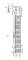
例示されている実施例においては、装置10は、図示しているように結合された、第1読み出し集積回路(ROIC)20と、第2ROIC22と、検出器アレイ24と、画像処理システム36とを有する。ROIC40及び42は、1つ又はそれ以上の列増幅器46及び48並びにバッファ30及び32をそれぞれ有する。ボンドパッド50及び52は、ROIC20及び22のそれぞれからの出力を提供する。
In the illustrated embodiment, the
例示としての実施例においては、第1ROICは第1単位セル40を有する。第2ROIC22は、第1ROIC20の外側に備えられ、第2単位セル42を有する。導電性鉛直方向相互接続アクセス(ビア)50が、第2ROIC22を通って、且つ第1ROIC20の中に、恐らくそれを通って備えられる。検出器アレイ24は第2ROIC22の外側に備えられ、検出器画素38を有する。各々の検出器画素38は、光を検出することに応答して電流を発生し、ビア50にその電流を流し、そのビアは、第1単位セル40及び第2単位セル42にその信号を送信する。列アンプ46及び48は単位セル40及び42のそれぞれの出力を増幅する。ボンドパッド50及び52は、列アンプ46及び48のそれぞれからの増幅された出力を供給する。バッファ30及び32は、ROIC20及び22のそれぞれからの出力をバッファリングする。画像処理システム36は、バッファ30及び32から出力を受けて、画像の表示を開始するように用いられることが可能である出力から画像データを生成する。
In the exemplary embodiment, the first ROIC has a
特定の実施形態においては、検出器画素38、単位セル40及び42の各々は、相補型金属酸化膜半導体(CMOS)回路が形成される異なる基板に対応する異なる機能回路を表し得る。装置10の断面図は、検出器画素38の1つの行並びに単位セル40及び42のみを示している。しかしながら、検出器アレイ24及びROIC20及び22は、検出器画素38並びに単位セル40及び42のそれぞれの行及び列の何れかの適切な数を有することが可能である。
In certain embodiments, each of the
特定の実施形態においては、検出器アレイ24は検出器画素38のアレイを有する。その実施形態においては、検出器画素38は、単位セル40及び/又は42により操作されることが可能であるアナログ電気信号を検知し、そのアナログ電気信号に放射光を変換する光検出器を有する。検出器画素38は、何れかの適切な放射フラックスの光を検出することが可能である。例えば、検出器画素38は、より高いフラックス(例えば、1015フォトン/cm2・sec)の光及び/又はより低いフラックスの光(例えば、1015フォトン/cm2・sec)を検出することが可能である。
In certain embodiments,
検出器画素38は何れかの適切な波長帯域の光を検出することが可能である。波長帯域の例には、短波長の赤外線(IR)(SWIR)(約1000乃至3000nm)、中波長IR(MWIR)(約3000乃至8000nm)、長波長IR(LWIR)(約7000乃至14,000nm)及び超長波長IR(VLWIR)(約12,000乃至30,000nm)並びにIR帯域の長波長側又は短波長側の帯域がある。
The
検出器画素38は、共通波長帯域に対して感応することが可能である、又は、1つの波長帯域に対して感応する画素の集合と、1つ又はそれ以上の他の波長帯域に対して感応する1つ又はそれ以上の画素の他の集合とを有することが可能である。第1波長帯域及び第2波長帯域は何れかの適切な波長帯域であることが可能である。例えば、第1波長帯域はSWIRであり、第2波長帯域はMWIRであることが可能である。
The
検出器アレイ24は何れかの適切な輝度の光を検出することが可能である。特定の実施形態においては、検出器アレイ24は、輝度が広ダイナミックレンジである光(例えば、赤外線)を検出することが可能である。例えば、検出器アレイ24は、値xを有するダイナミックレンジを有することが可能であり、ここでは、xは60乃至90dB、90乃至120dB又は120dB以上の値である。
The
特定の実施形態においては、ROIC20又は22は、検出器アレイ24と連結する電子回路マルチプレクサであり、アナログダイナミックレンジ管理回路として機能する。ROIC20又は22は、各々が検出器画素38にバイアスを掛ける単位セル40又は42のアレイを有する。単位セル40又は42は、検出器画素38から受けた電荷をコンデンサに充電する。第1ROIC20は第1単位セル40を有し、第2ROIC22は第2単位セル42を有する。単位セルの例については、図2を参照して説明する。
In certain embodiments,
特定の実施形態においては、ROIC20又は22は、シリコンに基づく基板により構成されることが可能である。CMOS回路は、材料の層のエッチング、成長及び処理により基板の外側に形成されることが可能である。検出器画素38のアレイは、ROIC20又は22に対してハイブリダイゼーションさせることが可能である。ROIC20又は22の特定の回路は検出器画素38と一体的に形成されることが可能である、又は検出器画素38と別個に形成されることが可能である。
In certain embodiments, the
特定の実施形態においては、一のROIC(第1又は第2ROIC)は高フラックス検知ROIC(又は高フラックス検知低消費電力ROIC)として機能することが可能であり、他のROIC(第2又は第1ROIC)は低フラックス検知ROIC(又は低フラックス検知高消費電力ROIC)として機能することが可能である。例えば、第1ROIC20は高フラックス検知ROICとして機能し、第2ROIC22は低フラックス検知ROICとして機能することが可能である。
In certain embodiments, one ROIC (first or second ROIC) can function as a high flux sensing ROIC (or high flux sensing low power ROIC) and the other ROIC (second or first ROIC). ) Can function as a low flux detection ROIC (or low flux detection high power consumption ROIC). For example, the
高フラックスROICは、より高いフラックスの光を捕捉するように電流を処理することが可能である。特定の実施形態においては、高フラックスROICは、低フラックスROICより消費電力が低いROICであることが可能である。実施例は、直接注入(DI)単位セルを有する。特定の実施形態においては、サブフレーム平均化(SFA)が、より大きい容量性のバケットサイズをもたらすより長い全集積時間を可能にするために、複数の短いサブフレーム集積を平均化するように用いられることが可能である。 High flux ROICs can handle current to capture higher flux of light. In certain embodiments, a high flux ROIC can be a ROIC that consumes less power than a low flux ROIC. The embodiment has a direct injection (DI) unit cell. In certain embodiments, subframe averaging (SFA) is used to average multiple short subframe accumulations to allow longer total integration times resulting in a larger capacitive bucket size. It is possible to be
低フラックスROICは、より低いフラックスの光により生成される光電流を処理することが可能である。特定の実施形態においては、低フラックスROICは、高フラックスROICより消費電力が高いROICであることが可能である。実施例においては、容量性トランスインピーダンスアンプ(CTIA)と、バッファード直接注入(BDI)単位セルとを有する。特定の実施形態においては、マルチフレーム平均化(MFA)処理が、減少された入射フラックスを補償することが可能である複数のフレーム時間に亘って全集積時間を延長するように用いられることが可能である。 A low flux ROIC can handle the photocurrent generated by the lower flux of light. In certain embodiments, the low flux ROIC can be a ROIC that consumes more power than a high flux ROIC. The embodiment includes a capacitive transimpedance amplifier (CTIA) and a buffered direct injection (BDI) unit cell. In certain embodiments, a multiframe averaging (MFA) process can be used to extend the total integration time over multiple frame times that can compensate for the reduced incident flux. It is.
特定の実施形態においては、第1ROIC20は、第1波長帯域の光と関連する電流を処理することが可能であり、第2ROIC22は、第1波長帯域と同じ又はそれとは異なることが可能である第2波長帯域の光と関連する電流を処理することが可能である。ROIC20及び22は、何れかの適切な波長帯域、例えば、上記の波長帯域を処理することが可能である。
In certain embodiments, the
特定の実施形態においては、検出器アレイ24は、ROIC20及び22間で交替させることによりROIC20及び22に電流を流すことが可能である。例えば、検出器アレイ24は、第1時間期間の間、高フラックスROICとして機能する一のROICに、続いて、第2時間期間の間、低フラックスROICとして機能する他のROICに電流を流すことが可能である。第2時間期間は、第1時間期間より長い、短い、又はそれと等しいことが可能である。例えば、第2時間期間(低フラックスROIC)は第1時間期間(高フラックスROICのための)より長いことが可能である。
In certain embodiments, the
特定の実施例においては、異なる波長帯域のフレーム間で時間的位置合わせを達成することが可能であるスケジュールに従って、電流がROIC20及び22に流されることが可能である。その実施例においては、電流は、第1波長帯域(例えば、LWIR帯域)を積分する第1ROIC20に、及び第2波長帯域(例えば、MWIR帯域)を積分する第2ROIC22に流されることが可能である。電流が第2ROIC22に流される第2時間期間の前に及び後に存在する第1時間期間の間、電流が第1ROIC20に流されることが可能である。第1時間期間及び第2時間期間は何れかの適切な持続時間を有することが可能であり、第1時間期間は第2時間期間より長い、短い又はそれと同じであることが可能である。例えば、第1時間期間は約1msecであることが可能であり、第2時間期間は約2乃至5msecであることが可能である。
In certain embodiments, current can be passed through the ROICs 20 and 22 according to a schedule that can achieve temporal alignment between frames of different wavelength bands. In that embodiment, current can be passed to the
特定の実施形態においては、ROIC20及び22は、並列に処理して、完全なデータのアレイを出力することが可能である。完全なデータのアレイは、少なくとも殆どの又は全てのROICの単位セルからの出力を有するデータを参照することが可能である。完全なデータのアレイは、画像のフレームを生成するように用いられることが可能である。特定の実施形態においては、装置10は、第1ROIC20により生成されたデータの1つ又はそれ以上の第1フレームを出力し、続いて、第2ROIC22により生成されたデータの1つ又はそれ以上の第2フレームを出力することが可能である。
In certain embodiments,
特定の実施形態においては、1つ又はそれ以上の第1列アンプ46は第1ROIC20からの出力を増幅することが可能であり、1つ又はそれ以上の第2列アンプ48は第2ROIC22からの出力を増幅することが可能である。列アンプの実施例は、列当たりシングルエンド型CTIA又は差動型CTIAを、若しくは列アンプ当たり電圧モードアンプを有する。
In certain embodiments, one or more
特定の実施形態においては、1つ又はそれ以上の第1バッファ30は、第1ROIC20からの出力をバッファリングすることが可能であり、1つ又はそれ以上の第2バッファ32は、第2ROIC22からの出力をバッファリングすることが可能である。バッファの例には、ボルテージフォロア、シングルエンド型アンプ又は差動型アンプ等の電圧モードアンプがある。
In certain embodiments, one or more
特定の実施形態においては、画像処理システム36は、第1ROIC20により生成されたデータの1つ又はそれ以上の第1フレームと、第2ROIC22により生成されたデータの1つ又はそれ以上の第2フレームとを受けることが可能である。画像処理システム36は、何れかの適切な方法で画像を生成するようにデータの第1フレーム及び第2フレームを解析することが可能である。例えば、画像処理システムは、合成フレームデータを生成するように第1フレームデータ及び第2フレームデータを融合させて、その合成フレームデータから画像のフレームを生成することが可能である。
In certain embodiments, the
図2は、単位システム60の実施例を示している。その実施例においては、単位システム60は、単位セル40と、単位セル42と、検出器画素38とを有する。ビア50は、検出器画素38を単位セル40及び/又は単位セル42に電気的に結合させ、検出器画素38から単位セル40及び/又は単位セル42に電流を流すことが可能である。
FIG. 2 shows an embodiment of the
特定の実施形態においては、ビア50は、孔内に備えられた導電性材料を有する孔(開口又はアパーチャ等)であることが可能である。何れかの適切な導電性材料、例えば、絶縁性酸化物材料が用いられることが可能である。ビア50は、スルーシリコンビア(TSV)等の適切なビアである。ビア50は何れかの適切な形状を有することが可能である。例えば、ビア50は、基板の反対面における開口を有する、1つの基板のみにおいて開口を有する、又は何れの面にも開口を有さないことが可能である。 In certain embodiments, the via 50 can be a hole (such as an opening or aperture) with a conductive material provided in the hole. Any suitable conductive material can be used, for example, an insulating oxide material. The via 50 is a suitable via such as a through silicon via (TSV). Via 50 can have any suitable shape. For example, the via 50 can have an opening on the opposite side of the substrate, an opening on only one substrate, or no opening on either side.
図3は、単位システム60をより詳細に示している。図示している実施例においては、単位システム60は、検出器画素38と、単位セル40及び42と、図示されたように結合されたビア50とを有する。各々の単位セル40及び42は、スイッチ70と、回路80と、コンデンサ84と、ストレージアレイ72とを有する。ストレージアレイ72は、ROIC20又は22の単位セル40又は42からの出力を蓄えるストレージ要素90を有する。動作の実施例においては、検出器画素38は、光を検出し、光の検出に応答して電流を出力する。スイッチ70は、電流を単位セル40の方に及び/又はビア50を介して電流を方向付ける。単位セル40及び42は、ストレージ要素90に蓄えられる出力を生成するように、その電流を処理する。
FIG. 3 shows the
特定の実施形態においては、単位セル40又は42は、ランプ回路及びアナログ/ディジタル変換器(A/D)を有することが可能である回路80及びコンデンサ84を有することが可能である。コンデンサ84は、第1プレートと、反対側の第2プレートとを有することが可能である。ランプ回路は、コンデンサの第1プレートに電圧ランプを供給することが可能である。コンデンサの第2プレートは、検出器画素38から電流を受けることが可能である。A/Dは、コンデンサの第2プレートからアナログ出力を受け、ストレージ要素90にディジタル出力を供給する。カウンタが、単位セルのアレイの出力に対して並列に結合されることが可能であり、全体的な計数において各々のディジタルインバータからのディジタル出力を蓄積することが可能である。
In certain embodiments, the
スイッチ70は、少なくとも一部の単位セルに備えられ、ビア50に対する制御された接続を提供することが可能である。特定の実施形態においては、スイッチ70は、ROIC20及び22間で交替させることによりROIC20及び22に電流を流すことが可能である。例えば、スイッチ70は、第1時間期間の間、高フラックスROICとして機能する一のROICに、続いて、第2時間期間の間、低フラックスROICとして機能する他のROICに電流を流すことが可能である。第2時間期間は、第1時間期間より長い、短い、又はそれと同じであることが可能である。例えば、第2時間期間(低フラックスROICのための)は第1時間期間(高フラックスROICのための)より長いことが可能である。
The
特定の実施形態においては、スイッチ70は、第1時間期間の間、第1波長帯域のために用いられる一のROICに電流を流し、第2時間期間の間、第2波長帯域のために用いられる他のROICに電流を流すことが可能であり、第2波長帯域はより広い波長を有する。第2時間期間は、第1時間期間より長い、短い、又はそれと同じであることが可能である。例えば、第2時間期間(広波長のための)は第1時間期間(狭波長のための)より長いことが可能である。例えば、第1時間期間は1乃至100μsecの範囲内の値であることが可能であり、第2時間期間は1000乃至20000μsecの範囲内の値であることが可能である。
In certain embodiments, the
単位セル40又は42は何れかの適切な大きさ、例えば、20μmx20μmの正方形より小さいことが可能である。単位セル40又は42は、何れかの適切なフレームレート、例えば、30Hz、60Hz又はそれより大きいフレームレートで動作することが可能である。
The
修正、付加又は削除が、本発明の範囲から逸脱することなく、本明細書で開示されたシステム及び装置で行われることが可能である。それらのシステム及び装置の構成要素は、一体化される又は別個にされることが可能である。更に、システム及び装置の動作は、より多い、より少ない又は他の構成要素により実行されることが可能である。例えば、ROIC20又は22の動作は、2つ以上の構成要素により実行されることが可能である。更に、システム及び装置の動作は、ソフトウェア、ハードウェア及び/又は他のロジックを有する何れかの適切なロジックを用いて実行されることが可能である。本明細書で用いているように、表現“各々”においては、集合の各々のメンバー又は集合の副集合の各々のメンバーを引き合いに出す。
Modifications, additions or deletions can be made with the systems and apparatus disclosed herein without departing from the scope of the present invention. The components of these systems and devices can be integrated or separated. Moreover, the operation of the system and apparatus can be performed by more, fewer, or other components. For example, the operation of
修正、付加又は削除は、本発明の範囲から逸脱せずに、本明細書で開示されている方法に対して行われ得る。その方法は、より多い、少ないステップを、又は他のステップを有することが可能である。更に、ステップは、何れかの適切な順序で実行されることが可能である。 Modifications, additions or deletions may be made to the methods disclosed herein without departing from the scope of the invention. The method can have more, fewer steps, or other steps. Further, the steps can be performed in any suitable order.
本明細書において開示されているシステム及び装置の構成要素は、インタフェース、ロジック、メモリ及び/又は他の適切な要素を有することが可能である。インタフェースは入力を受信し、出力を送信し、その入力及び/又は出力を処理し、並びに/若しくは他の適切な動作を実行する。インタフェースはハードウェア及び/又はソフトウェアを有することが可能である。 The components of the systems and devices disclosed herein can include interfaces, logic, memory, and / or other suitable elements. The interface receives input, sends output, processes the input and / or output, and / or performs other suitable operations. The interface can comprise hardware and / or software.
ロジックは、構成要素の動作を実行する、例えば、入力から出力を生成する命令を実行する。ロジックは、ハードウェア、ソフトウェア及び/又は他のロジックを有することが可能である。ロジックは、1つ又はそれ以上の有体媒体において符号化されることが可能である。プロセッサのような特定のロジックが構成要素の動作を管理することが可能である。プロセッサの例としては、1つ又はそれ以上のコンピュータ、1つ又はそれ以上のマイクロプロセッサ、1つ又はそれ以上のアプリケーション及び/又は他のロジックを有する。 The logic executes the operations of the component, for example, executes instructions to generate output from input. The logic can comprise hardware, software and / or other logic. The logic can be encoded in one or more tangible media. Certain logic, such as a processor, can manage the operation of the component. Examples of processors include one or more computers, one or more microprocessors, one or more applications, and / or other logic.
特定の実施形態においては、実施形態の動作は、コンピュータプログラム、ソフトウェア、コンピュータ実行可能命令及び/又はコンピュータにより実行されることが可能である命令により実行されることが可能である。特定の実施形態においては、実施形態の動作は、記憶される、コンピュータプログラムにより具現される及び/又は符号化される、並びに/若しくは記憶された及び/若しくは符号化されたコンピュータプログラムを有する、1つ又はそれ以上のコンピュータ読み出し可能媒体により実行されることが可能である。 In certain embodiments, the operations of the embodiments can be performed by computer programs, software, computer-executable instructions and / or instructions that can be executed by a computer. In certain embodiments, the operations of the embodiments comprise a computer program stored, embodied and / or encoded by a computer program, and / or stored and / or encoded. It can be performed by one or more computer readable media.
メモリは命令を記憶する。メモリは、1つ又はそれ以上の非一時的媒体、有体記憶媒体、コンピュータ読み出し可能記憶媒体及び/又はコンピュータ実行可能記憶媒体記憶を有することが可能である。メモリの例としては、コンピュータメモリ(例えば、ランダムアクセスメモリ(RAM)又は読み出し専用メモリ(ROM))、大容量媒体(例えば、ハードディスク)、取り外し可能記憶媒体(例えば、コンパクトディスク(CD)又はディジタルビデオディスク(DVD))、データベース及び/又はネットワークストレージ(例えば、サーバ)並びに/若しくは他のコンピュータ読み出し可能媒体を有することが可能である。 The memory stores instructions. The memory may have one or more non-transitory media, tangible storage media, computer readable storage media, and / or computer executable storage media storage. Examples of memory include computer memory (eg, random access memory (RAM) or read only memory (ROM)), large capacity media (eg, hard disk), removable storage media (eg, compact disc (CD) or digital video). Disc (DVD)), database and / or network storage (eg, server) and / or other computer readable media may be included.
システム及び装置の構成要素は何れかの適切な通信ネットワークにより結合されることが可能である。通信ネットワークは、公衆交換電話網(PSTN)、公衆又は個人データネットワーク、ローカルエリアネットワーク(LAN)、メトロポリタンエリアネットワーク(MAN)、ワイドエリアネットワーク(WAN)、ローカル、域内又はグローバル通信、又はインターネットのようなコンピュータネットワーク、有線又は無線ネットワーク、企業イントラネット、他の適切な通信リンク、若しくは上記の何れかの組み合わせ、の1つ又はそれ以上の全て又は一部を有することが可能である。 System and apparatus components may be coupled by any suitable communication network. The communication network can be a public switched telephone network (PSTN), a public or personal data network, a local area network (LAN), a metropolitan area network (MAN), a wide area network (WAN), local, regional or global communications, or the Internet. A computer network, a wired or wireless network, a corporate intranet, other suitable communication links, or any combination of any of the above, all or part of.
本明細書においては、特定の実施形態について詳述しているが、それらの実施形態の代替及び置き換えが可能であることが当業者には理解できる。従って、上記の実施形態の詳述は本発明を制限するものではない。他の変形、置き換え及び修正が、本発明の趣旨及び範囲から逸脱することなく、可能であり、同時提出の特許請求の範囲によって規定されるものである。 Although specific embodiments are described in detail herein, those skilled in the art will recognize that these embodiments can be substituted and replaced. Therefore, the detailed description of the above embodiment does not limit the present invention. Other variations, substitutions, and modifications are possible without departing from the spirit and scope of the present invention and are defined by the appended claims.
36 画像処理システム
38 検出器アレイ
40 単位セル
42 単位セル
50 ボンドパッド(ビア)
52 ボンドパッド
60 単位システム
72 ストレージアレイ
80 回路
90 ストレージ要素
36
52
Claims (14)
前記第1のROIC上に備えられ、複数の第2単位セルを有する第2のROICと、
前記第2のROICを貫通し且つ前記第1のROICの少なくとも一部に入るように備えられる複数の導電性ビアと、
前記第2のROIC上に備えられ、複数の検出器画素を有する検出器アレイであって、前記複数の検出器画素の各々は、光を受光したことに応答して電流を生成し、前記複数の導電性ビアのうち対応する導電性ビアに前記電流を送る、検出器アレイと、
を有し、前記複数の第1単位セルの各々は、前記電流を処理する第1回路と、前記第1回路を、前記複数の導電性ビアのうち対応する導電性ビアに、第1の時間期間の間電気的に接続する第1スイッチとを有し、
前記複数の第2単位セルの各々は、前記電流を処理する第2回路と、前記第2回路を、前記複数の導電性ビアのうち対応する導電性ビアに、第1の時間期間に続く第2の時間期間の間電気的に接続する第2スイッチとを有し、
前記検出器アレイは、単位面積及び単位時間当たりのフォトン数が所定値より高い高フラックス光及び前記所定値より低い低フラックス光のうち一方を、前記第1の時間期間の間に受光し、前記高フラックス光及び低フラックス光のうち他方を、前記第2の時間期間の間に受光する、装置。 A first readout integrated circuit having a plurality of first unit cell (ROIC),
Provided on the first ROIC, a second ROIC having a plurality of second unit cells,
A plurality of conductive vias provided to enter at least a portion of the second through the ROIC且previous SL first ROIC,
Provided on the second ROIC, a detector array having a plurality of detector pixels, each of the plurality of detector pixel generates a current in response particular to receive light, said plurality that feed the current to the corresponding conductive vias of the conductive vias, a detector array,
Each of the plurality of first unit cells includes a first circuit for processing the current and the first circuit to a corresponding conductive via among the plurality of conductive vias for a first time. A first switch electrically connected for a period of time,
Each of the plurality of second unit cells includes a second circuit that processes the current, and a second circuit that is connected to a corresponding conductive via among the plurality of conductive vias in a first time period. A second switch electrically connected for two time periods;
The detector array receives one of a high flux light whose unit area and the number of photons per unit time are higher than a predetermined value and a low flux light lower than the predetermined value during the first time period, An apparatus for receiving the other of the high flux light and the low flux light during the second time period .
前記第1のROIC上に備えられ、複数の第2単位セルを有する第2のROICと、 A second ROIC provided on the first ROIC and having a plurality of second unit cells;
前記第2のROICを貫通し且つ前記第1のROICの少なくとも一部に入るように備えられる複数の導電性ビアと、 A plurality of conductive vias provided to penetrate through the second ROIC and into at least a portion of the first ROIC;
前記第2のROIC上に備えられ、複数の検出器画素を有する検出器アレイであって、前記複数の検出器画素の各々は、光を受光したことに応答して電流を生成し、前記複数の導電性ビアのうち対応する導電性ビアに前記電流を送る、検出器アレイと、 A detector array provided on the second ROIC and having a plurality of detector pixels, each of the plurality of detector pixels generating a current in response to receiving light, the plurality of detector pixels A detector array for sending the current to a corresponding one of the conductive vias;
を有し、前記複数の第1単位セルの各々は、前記電流を処理する第1回路と、前記第1回路を、前記複数の導電性ビアのうち対応する導電性ビアに、第1の時間期間の間電気的に接続する第1スイッチとを有し、 Each of the plurality of first unit cells includes a first circuit for processing the current and the first circuit to a corresponding conductive via among the plurality of conductive vias for a first time. A first switch electrically connected for a period of time,
前記複数の第2単位セルの各々は、前記電流を処理する第2回路と、前記第2回路を、前記複数の導電性ビアのうち対応する導電性ビアに、第1の時間期間に続く第2の時間期間の間電気的に接続する第2スイッチとを有し、 Each of the plurality of second unit cells includes a second circuit that processes the current, and a second circuit that is connected to a corresponding conductive via among the plurality of conductive vias in a first time period. A second switch electrically connected for two time periods;
前記検出器アレイは、第1の波長帯域に属する第1波長光及び前記第1の波長帯域とは異なる第2の波長帯域に属する第2波長光のうち一方を、前記第1の時間期間の間に受光し、前記第1波長光及び第2波長光のうち他方を、前記第2の時間期間の間に受光する、装置。 The detector array receives one of a first wavelength light belonging to a first wavelength band and a second wavelength light belonging to a second wavelength band different from the first wavelength band, in the first time period. And receiving the other of the first wavelength light and the second wavelength light during the second time period.
前記第2のROICに結合され、前記第2のROICからの出力を増幅するように形成される1つ以上の第2列アンプと、
を更に有する、請求項1又は2に記載の装置。 And coupled to said first ROIC, first column amplifier on one or more formed to amplify the output from the first ROIC,
And coupled to said second ROIC, second column amplifier on one or more formed to amplify the output from the second ROIC,
Further comprising a device according to claim 1 or 2.
前記第2のROICに結合され、前記第2のROICからの出力をバッファリングするように形成される1つ以上の第2バッファと、
を更に有する、請求項1又は2に記載の装置。 Coupled to said first ROIC, a first buffer on one or more of the output is formed so as to buffer from the first ROIC,
Coupled to said second ROIC, and the second buffer on one or more formed the output from the second ROIC to buffer,
Further comprising a device according to claim 1 or 2.
前記第1のROIC上に備えられ、複数の第2単位セルを有する第2のROICと、 A second ROIC provided on the first ROIC and having a plurality of second unit cells;
前記第2のROICを貫通し且つ前記第1のROICの少なくとも一部に入るように備えられる複数の導電性ビアと、 A plurality of conductive vias provided to penetrate through the second ROIC and into at least a portion of the first ROIC;
前記第2のROIC上に備えられ、複数の検出器画素を有する検出器アレイと、 A detector array provided on the second ROIC and having a plurality of detector pixels;
を有する装置が実行する方法であって、 A method performed by a device having:
第1の時間期間の間に、前記複数の検出器画素の各々が、単位面積及び単位時間当たりのフォトン数が所定値より高い高フラックス光及び前記所定値より低い低フラックス光のうち一方を受光したことに応答して電流を生成し、前記複数の導電性ビアのうち対応する導電性ビアに該電流を送り、前記複数の第1単位セルの各々が、前記第1の時間期間の間では導通状態である第1スイッチを介して該電流を受け、第1回路により該電流を処理するステップと、 During the first time period, each of the plurality of detector pixels receives one of a high flux light whose unit area and the number of photons per unit time are higher than a predetermined value and a low flux light lower than the predetermined value. In response, the current is generated, and the current is sent to a corresponding one of the plurality of conductive vias, and each of the plurality of first unit cells is in the first time period. Receiving the current through a first switch in a conducting state and processing the current by a first circuit;
前記第1の時間期間に続く第2の時間期間の間に、前記複数の検出器画素の各々が、前記高フラックス光及び低フラックス光のうち他方を受光したことに応答して電流を生成し、前記複数の導電性ビアのうち対応する導電性ビアに該電流を送り、前記複数の第2単位セルの各々が、前記第2の時間期間の間では導通状態である第2スイッチを介して該電流を受け、第2回路により前記電流を処理するステップと、 During a second time period following the first time period, each of the plurality of detector pixels generates a current in response to receiving the other of the high flux light and the low flux light. The current is sent to a corresponding one of the plurality of conductive vias, and each of the plurality of second unit cells is connected through a second switch that is in a conductive state during the second time period. Receiving the current and processing the current by a second circuit;
を有する方法。 Having a method.
前記第1のROIC上に備えられ、複数の第2単位セルを有する第2のROICと、 A second ROIC provided on the first ROIC and having a plurality of second unit cells;
前記第2のROICを貫通し且つ前記第1のROICの少なくとも一部に入るように備えられる複数の導電性ビアと、 A plurality of conductive vias provided to penetrate through the second ROIC and into at least a portion of the first ROIC;
前記第2のROIC上に備えられ、複数の検出器画素を有する検出器アレイと、 A detector array provided on the second ROIC and having a plurality of detector pixels;
を有する装置が実行する方法であって、 A method performed by a device having:
第1の時間期間の間に、前記複数の検出器画素の各々が、第1の波長帯域に属する第1波長光及び前記第1の波長帯域とは異なる第2の波長帯域に属する第2波長光のうち一方を受光したことに応答して電流を生成し、前記複数の導電性ビアのうち対応する導電性ビアに該電流を送り、前記複数の第1単位セルの各々が、前記第1の時間期間の間では導通状態である第1スイッチを介して該電流を受け、第1回路により該電流を処理するステップと、 During the first time period, each of the plurality of detector pixels includes a first wavelength light belonging to a first wavelength band and a second wavelength belonging to a second wavelength band different from the first wavelength band. A current is generated in response to receiving one of the lights, and the current is sent to a corresponding one of the plurality of conductive vias, and each of the plurality of first unit cells is configured to receive the first unit cell. Receiving the current through a first switch that is in a conducting state during a period of time and processing the current by a first circuit;
前記第1の時間期間に続く第2の時間期間の間に、前記複数の検出器画素の各々が、前記第1波長光及び第2波長光のうち他方を受光したことに応答して電流を生成し、前記複数の導電性ビアのうち対応する導電性ビアに該電流を送り、前記複数の第2単位セルの各々が、前記第2の時間期間の間では導通状態である第2スイッチを介して該電流を受け、第2回路により該電流を処理するステップと、 During a second time period following the first time period, each of the plurality of detector pixels receives a current in response to receiving the other of the first wavelength light and the second wavelength light. Generating a second switch in which each of the plurality of second unit cells is in a conductive state during the second time period. Receiving the current through and processing the current by a second circuit;
を有する方法。 Having a method.
前記第2のROICに結合される1つ以上の第2列アンプにより、前記第2のROICからの出力を増幅するステップと、
を更に有する、請求項8又は9に記載の方法。 The first column amplifier on one or more that will be coupled to the first ROIC, a step for amplifying the output from the first ROIC,
The second column amplifier on one or more that will be coupled to the second ROIC, a step for amplifying the output from said second ROIC,
10. The method according to claim 8 or 9 , further comprising:
前記第2のROICに結合される1つ以上の第2バッファにより、前記第2のROICからの出力をバッファリングするステップと
を更に有する、請求項8又は9に記載の方法。 By one or more of the first buffer that will be coupled to the first ROIC, a step of buffering the output from the first ROIC,
Wherein the second second buffers on one or more that will be coupled to the ROIC, further comprising the step of buffering the output from the second ROIC, The method according to claim 8 or 9.
前記第2のROICにより生成されるデータの1つ以上の第2フレームを出力するステップと、
を更に有する、請求項8又は9に記載の方法。 And outputting the first frame on one or more of the data that is generated by the first ROIC,
And outputting the second frame on one or more of data to which the Ru generated by the second ROIC,
10. The method according to claim 8 or 9 , further comprising:
Applications Claiming Priority (2)
| Application Number | Priority Date | Filing Date | Title |
|---|---|---|---|
| US12/952,282 | 2010-11-23 | ||
| US12/952,282 US8415623B2 (en) | 2010-11-23 | 2010-11-23 | Processing detector array signals using stacked readout integrated circuits |
Publications (3)
| Publication Number | Publication Date |
|---|---|
| JP2012114439A JP2012114439A (en) | 2012-06-14 |
| JP2012114439A5 JP2012114439A5 (en) | 2014-01-23 |
| JP5717612B2 true JP5717612B2 (en) | 2015-05-13 |
Family
ID=45094482
Family Applications (1)
| Application Number | Title | Priority Date | Filing Date |
|---|---|---|---|
| JP2011254773A Active JP5717612B2 (en) | 2010-11-23 | 2011-11-22 | Processing apparatus and processing method |
Country Status (5)
| Country | Link |
|---|---|
| US (1) | US8415623B2 (en) |
| EP (1) | EP2456193B1 (en) |
| JP (1) | JP5717612B2 (en) |
| IL (1) | IL216363A (en) |
| TW (1) | TWI531242B (en) |
Families Citing this family (7)
| Publication number | Priority date | Publication date | Assignee | Title |
|---|---|---|---|---|
| US8637800B2 (en) | 2011-04-19 | 2014-01-28 | Altasens, Inc. | Image sensor with hybrid heterostructure |
| US9310495B2 (en) * | 2011-05-04 | 2016-04-12 | Oy Ajat Ltd. | Photon/energy identifying X-ray and gamma ray imaging device (“PID”) with a two dimensional array of pixels and system therefrom |
| US8773562B1 (en) * | 2013-01-31 | 2014-07-08 | Apple Inc. | Vertically stacked image sensor |
| US9110136B2 (en) | 2013-09-27 | 2015-08-18 | Taiwan Semiconductor Manufacturing Company, Ltd. | Circuit and method for monolithic stacked integrated circuit testing |
| US20180376044A1 (en) * | 2017-06-22 | 2018-12-27 | Robert Bosch Gmbh | Device Having A CMOS VL and IR Imaging System |
| US10883804B2 (en) * | 2017-12-22 | 2021-01-05 | Ams Sensors Uk Limited | Infra-red device |
| US20200344426A1 (en) * | 2019-04-15 | 2020-10-29 | Owl Autonomous Imaging, Inc. | Thermal ranging devices and methods |
Family Cites Families (26)
| Publication number | Priority date | Publication date | Assignee | Title |
|---|---|---|---|---|
| US6456326B2 (en) | 1994-01-28 | 2002-09-24 | California Institute Of Technology | Single chip camera device having double sampling operation |
| US5512750A (en) * | 1994-06-03 | 1996-04-30 | Martin Marietta Corporation | A-dual band IR sensor having two monolithically integrated staring detector arrays for simultaneous, coincident image readout |
| DE69628187D1 (en) | 1995-11-07 | 2003-06-18 | California Inst Of Techn | IMAGE SENSOR WITH LINEAR OUTPUT WITH LARGE DYNAMIC RANGE |
| US5892541A (en) | 1996-09-10 | 1999-04-06 | Foveonics, Inc. | Imaging system and method for increasing the dynamic range of an array of active pixel sensor cells |
| FR2759494B1 (en) * | 1997-02-07 | 1999-03-05 | Commissariat Energie Atomique | MULTI-COLOR PHOTON RADIATION DETECTOR |
| US6493030B1 (en) | 1998-04-08 | 2002-12-10 | Pictos Technologies, Inc. | Low-noise active pixel sensor for imaging arrays with global reset |
| US6078037A (en) | 1998-04-16 | 2000-06-20 | Intel Corporation | Active pixel CMOS sensor with multiple storage capacitors |
| US6875975B2 (en) * | 1999-12-24 | 2005-04-05 | Bae Systems Information And Electronic Systems Integration Inc | Multi-color, multi-focal plane optical detector |
| JP3713418B2 (en) * | 2000-05-30 | 2005-11-09 | 光正 小柳 | Manufacturing method of three-dimensional image processing apparatus |
| US6504141B1 (en) | 2000-09-29 | 2003-01-07 | Rockwell Science Center, Llc | Adaptive amplifier circuit with enhanced dynamic range |
| US6924841B2 (en) | 2001-05-02 | 2005-08-02 | Agilent Technologies, Inc. | System and method for capturing color images that extends the dynamic range of an image sensor using first and second groups of pixels |
| US6885002B1 (en) | 2001-08-31 | 2005-04-26 | Raytheon Company | IRFPA ROIC with dual TDM reset integrators and sub-frame averaging functions per unit cell |
| US6864965B2 (en) * | 2002-03-12 | 2005-03-08 | Bae Systems Information And Electronic Systems Integration Inc. | Dual-mode focal plane array for missile seekers |
| US20060055800A1 (en) * | 2002-12-18 | 2006-03-16 | Noble Device Technologies Corp. | Adaptive solid state image sensor |
| US7586074B2 (en) | 2003-02-17 | 2009-09-08 | Raytheon Company | Multi-mode high capacity dual integration direct injection detector input circuit |
| US7492399B1 (en) * | 2004-02-17 | 2009-02-17 | Raytheon Company | High dynamic range dual mode charge transimpedance amplifier/source follower per detector input circuit |
| US7091531B2 (en) | 2004-04-07 | 2006-08-15 | Micron Technology, Inc. | High dynamic range pixel amplifier |
| US7723815B1 (en) * | 2004-07-09 | 2010-05-25 | Raytheon Company | Wafer bonded composite structure for thermally matching a readout circuit (ROIC) and an infrared detector chip both during and after hybridization |
| JP3976754B2 (en) | 2004-07-13 | 2007-09-19 | マイクロン テクノロジー,インコーポレイテッド | Wide dynamic range imaging device with selective reading |
| US7551059B2 (en) * | 2005-01-06 | 2009-06-23 | Goodrich Corporation | Hybrid infrared detector array and CMOS readout integrated circuit with improved dynamic range |
| US7095355B1 (en) | 2005-05-09 | 2006-08-22 | Raytheon Company | Low power ADC for imaging arrays |
| US20070102622A1 (en) | 2005-07-01 | 2007-05-10 | Olsen Richard I | Apparatus for multiple camera devices and method of operating same |
| JP4901320B2 (en) * | 2006-06-13 | 2012-03-21 | 三菱電機株式会社 | 2-wavelength image sensor |
| US7592593B2 (en) * | 2006-07-26 | 2009-09-22 | Northrop Grumman Corporation | Multi-band focal plane array |
| US7616243B2 (en) | 2007-03-07 | 2009-11-10 | Altasens, Inc. | Method and apparatus for improving and controlling dynamic range in an image sensor |
| US8154099B2 (en) * | 2009-08-19 | 2012-04-10 | Raytheon Company | Composite semiconductor structure formed using atomic bonding and adapted to alter the rate of thermal expansion of a substrate |
-
2010
- 2010-11-23 US US12/952,282 patent/US8415623B2/en active Active
-
2011
- 2011-11-14 IL IL216363A patent/IL216363A/en active IP Right Grant
- 2011-11-21 EP EP11190023.9A patent/EP2456193B1/en active Active
- 2011-11-22 JP JP2011254773A patent/JP5717612B2/en active Active
- 2011-11-22 TW TW100142703A patent/TWI531242B/en active
Also Published As
| Publication number | Publication date |
|---|---|
| IL216363A (en) | 2016-10-31 |
| EP2456193A3 (en) | 2014-08-20 |
| US8415623B2 (en) | 2013-04-09 |
| TWI531242B (en) | 2016-04-21 |
| JP2012114439A (en) | 2012-06-14 |
| TW201230795A (en) | 2012-07-16 |
| EP2456193A2 (en) | 2012-05-23 |
| EP2456193B1 (en) | 2020-07-08 |
| US20120126121A1 (en) | 2012-05-24 |
| IL216363A0 (en) | 2012-02-29 |
Similar Documents
| Publication | Publication Date | Title |
|---|---|---|
| JP5717612B2 (en) | Processing apparatus and processing method | |
| TWI545954B (en) | Negative biased substrate for pixels in stacked image sensors | |
| US9570486B2 (en) | Solid-state imaging device and switching circuit | |
| EP3430648B1 (en) | Stacked backside-illuminated quanta image sensor with cluster-parallel readout | |
| US20130107095A1 (en) | Solid-state imaging device | |
| TW201004326A (en) | Suppression of row-wise noise in CMOS image sensors | |
| US10777602B2 (en) | Pixel circuit | |
| TW201519420A (en) | Buffered direct injection pixel for infrared detector arrays | |
| US11343439B2 (en) | High dynamic range imaging pixels with multiple photodiodes | |
| US20230007208A1 (en) | Methods and systems of low power facial recognition | |
| US10277838B2 (en) | Monolithic visible/IR fused low light level imaging sensor | |
| US10084980B2 (en) | Solid-state image sensor and camera | |
| JP2012114439A5 (en) | ||
| TW202101969A (en) | Solid-state imaging element | |
| JP2020181932A (en) | Solid-state image sensor, manufacturing method of solid-state image sensor, and electronic device | |
| KR20130074501A (en) | Image sensor and operation method of the same | |
| US11539904B2 (en) | Image sensor and electronic camera | |
| KR20080085798A (en) | Laminating type thermovision sensor device | |
| US11451751B2 (en) | Solid-state image pickup device and image pickup device | |
| WO2022004269A1 (en) | Photodetector and electronic device | |
| WO2020050195A1 (en) | Solid-state imaging element and electronic device | |
| JP2004363437A (en) | Amplification type solid state image pickup device | |
| KR100868191B1 (en) | Charge Coupled Device with no Horizontal Charge Coupled Device | |
| JP2017103420A (en) | Imaging device |
Legal Events
| Date | Code | Title | Description |
|---|---|---|---|
| A521 | Request for written amendment filed |
Free format text: JAPANESE INTERMEDIATE CODE: A523 Effective date: 20131202 |
|
| A621 | Written request for application examination |
Free format text: JAPANESE INTERMEDIATE CODE: A621 Effective date: 20131202 |
|
| A977 | Report on retrieval |
Free format text: JAPANESE INTERMEDIATE CODE: A971007 Effective date: 20140916 |
|
| A131 | Notification of reasons for refusal |
Free format text: JAPANESE INTERMEDIATE CODE: A131 Effective date: 20141104 |
|
| A521 | Request for written amendment filed |
Free format text: JAPANESE INTERMEDIATE CODE: A523 Effective date: 20150122 |
|
| TRDD | Decision of grant or rejection written | ||
| A01 | Written decision to grant a patent or to grant a registration (utility model) |
Free format text: JAPANESE INTERMEDIATE CODE: A01 Effective date: 20150217 |
|
| A61 | First payment of annual fees (during grant procedure) |
Free format text: JAPANESE INTERMEDIATE CODE: A61 Effective date: 20150317 |
|
| R150 | Certificate of patent or registration of utility model |
Ref document number: 5717612 Country of ref document: JP Free format text: JAPANESE INTERMEDIATE CODE: R150 |
|
| R250 | Receipt of annual fees |
Free format text: JAPANESE INTERMEDIATE CODE: R250 |
|
| R250 | Receipt of annual fees |
Free format text: JAPANESE INTERMEDIATE CODE: R250 |
|
| R250 | Receipt of annual fees |
Free format text: JAPANESE INTERMEDIATE CODE: R250 |
|
| R250 | Receipt of annual fees |
Free format text: JAPANESE INTERMEDIATE CODE: R250 |
|
| R250 | Receipt of annual fees |
Free format text: JAPANESE INTERMEDIATE CODE: R250 |
|
| R250 | Receipt of annual fees |
Free format text: JAPANESE INTERMEDIATE CODE: R250 |
|
| R250 | Receipt of annual fees |
Free format text: JAPANESE INTERMEDIATE CODE: R250 |