JP5703590B2 - Manufacturing method of semiconductor device - Google Patents
Manufacturing method of semiconductor device Download PDFInfo
- Publication number
- JP5703590B2 JP5703590B2 JP2010108111A JP2010108111A JP5703590B2 JP 5703590 B2 JP5703590 B2 JP 5703590B2 JP 2010108111 A JP2010108111 A JP 2010108111A JP 2010108111 A JP2010108111 A JP 2010108111A JP 5703590 B2 JP5703590 B2 JP 5703590B2
- Authority
- JP
- Japan
- Prior art keywords
- silicon nitride
- nitride film
- semiconductor device
- film
- manufacturing
- Prior art date
- Legal status (The legal status is an assumption and is not a legal conclusion. Google has not performed a legal analysis and makes no representation as to the accuracy of the status listed.)
- Expired - Fee Related
Links
- 239000004065 semiconductor Substances 0.000 title claims description 202
- 238000004519 manufacturing process Methods 0.000 title claims description 132
- 229910052581 Si3N4 Inorganic materials 0.000 claims description 470
- HQVNEWCFYHHQES-UHFFFAOYSA-N silicon nitride Chemical compound N12[Si]34N5[Si]62N3[Si]51N64 HQVNEWCFYHHQES-UHFFFAOYSA-N 0.000 claims description 470
- 238000000034 method Methods 0.000 claims description 118
- 229910017855 NH 4 F Inorganic materials 0.000 claims description 63
- 239000007789 gas Substances 0.000 claims description 52
- 239000000758 substrate Substances 0.000 claims description 48
- 238000010438 heat treatment Methods 0.000 claims description 43
- 238000009832 plasma treatment Methods 0.000 claims description 26
- QVGXLLKOCUKJST-UHFFFAOYSA-N atomic oxygen Chemical compound [O] QVGXLLKOCUKJST-UHFFFAOYSA-N 0.000 claims description 24
- 239000001301 oxygen Substances 0.000 claims description 24
- 229910052760 oxygen Inorganic materials 0.000 claims description 24
- 238000005530 etching Methods 0.000 description 88
- 238000009792 diffusion process Methods 0.000 description 37
- 239000010410 layer Substances 0.000 description 37
- 238000001723 curing Methods 0.000 description 23
- 230000004048 modification Effects 0.000 description 22
- 238000012986 modification Methods 0.000 description 22
- 239000012535 impurity Substances 0.000 description 21
- 230000007423 decrease Effects 0.000 description 15
- 230000015572 biosynthetic process Effects 0.000 description 14
- 238000002955 isolation Methods 0.000 description 13
- 239000002019 doping agent Substances 0.000 description 12
- 238000005229 chemical vapour deposition Methods 0.000 description 10
- 238000005468 ion implantation Methods 0.000 description 9
- 229910021332 silicide Inorganic materials 0.000 description 7
- FVBUAEGBCNSCDD-UHFFFAOYSA-N silicide(4-) Chemical compound [Si-4] FVBUAEGBCNSCDD-UHFFFAOYSA-N 0.000 description 7
- 229910000577 Silicon-germanium Inorganic materials 0.000 description 6
- LEVVHYCKPQWKOP-UHFFFAOYSA-N [Si].[Ge] Chemical compound [Si].[Ge] LEVVHYCKPQWKOP-UHFFFAOYSA-N 0.000 description 6
- 230000001133 acceleration Effects 0.000 description 6
- KRHYYFGTRYWZRS-UHFFFAOYSA-M Fluoride anion Chemical compound [F-] KRHYYFGTRYWZRS-UHFFFAOYSA-M 0.000 description 5
- XKRFYHLGVUSROY-UHFFFAOYSA-N Argon Chemical compound [Ar] XKRFYHLGVUSROY-UHFFFAOYSA-N 0.000 description 4
- VYPSYNLAJGMNEJ-UHFFFAOYSA-N Silicium dioxide Chemical class O=[Si]=O VYPSYNLAJGMNEJ-UHFFFAOYSA-N 0.000 description 4
- 238000006243 chemical reaction Methods 0.000 description 4
- 238000001020 plasma etching Methods 0.000 description 4
- 229910052814 silicon oxide Inorganic materials 0.000 description 4
- WGTYBPLFGIVFAS-UHFFFAOYSA-M tetramethylammonium hydroxide Chemical compound [OH-].C[N+](C)(C)C WGTYBPLFGIVFAS-UHFFFAOYSA-M 0.000 description 4
- 239000011800 void material Substances 0.000 description 4
- 229910052751 metal Inorganic materials 0.000 description 3
- 239000002184 metal Substances 0.000 description 3
- 238000004151 rapid thermal annealing Methods 0.000 description 3
- 239000000243 solution Substances 0.000 description 3
- 238000001039 wet etching Methods 0.000 description 3
- DDFHBQSCUXNBSA-UHFFFAOYSA-N 5-(5-carboxythiophen-2-yl)thiophene-2-carboxylic acid Chemical compound S1C(C(=O)O)=CC=C1C1=CC=C(C(O)=O)S1 DDFHBQSCUXNBSA-UHFFFAOYSA-N 0.000 description 2
- QGZKDVFQNNGYKY-UHFFFAOYSA-N Ammonia Chemical compound N QGZKDVFQNNGYKY-UHFFFAOYSA-N 0.000 description 2
- MYMOFIZGZYHOMD-UHFFFAOYSA-N Dioxygen Chemical compound O=O MYMOFIZGZYHOMD-UHFFFAOYSA-N 0.000 description 2
- PXHVJJICTQNCMI-UHFFFAOYSA-N Nickel Chemical compound [Ni] PXHVJJICTQNCMI-UHFFFAOYSA-N 0.000 description 2
- XUIMIQQOPSSXEZ-UHFFFAOYSA-N Silicon Chemical compound [Si] XUIMIQQOPSSXEZ-UHFFFAOYSA-N 0.000 description 2
- QAOWNCQODCNURD-UHFFFAOYSA-N Sulfuric acid Chemical compound OS(O)(=O)=O QAOWNCQODCNURD-UHFFFAOYSA-N 0.000 description 2
- 239000007864 aqueous solution Substances 0.000 description 2
- 229910052786 argon Inorganic materials 0.000 description 2
- OEYIOHPDSNJKLS-UHFFFAOYSA-N choline Chemical compound C[N+](C)(C)CCO OEYIOHPDSNJKLS-UHFFFAOYSA-N 0.000 description 2
- 229960001231 choline Drugs 0.000 description 2
- 230000000052 comparative effect Effects 0.000 description 2
- 238000010586 diagram Methods 0.000 description 2
- 229910001882 dioxygen Inorganic materials 0.000 description 2
- 238000011156 evaluation Methods 0.000 description 2
- 239000001307 helium Substances 0.000 description 2
- 229910052734 helium Inorganic materials 0.000 description 2
- SWQJXJOGLNCZEY-UHFFFAOYSA-N helium atom Chemical compound [He] SWQJXJOGLNCZEY-UHFFFAOYSA-N 0.000 description 2
- 239000000463 material Substances 0.000 description 2
- 239000012528 membrane Substances 0.000 description 2
- 238000005268 plasma chemical vapour deposition Methods 0.000 description 2
- 229910021420 polycrystalline silicon Inorganic materials 0.000 description 2
- 229920005591 polysilicon Polymers 0.000 description 2
- 229910052710 silicon Inorganic materials 0.000 description 2
- 239000010703 silicon Substances 0.000 description 2
- 239000002344 surface layer Substances 0.000 description 2
- VHUUQVKOLVNVRT-UHFFFAOYSA-N Ammonium hydroxide Chemical compound [NH4+].[OH-] VHUUQVKOLVNVRT-UHFFFAOYSA-N 0.000 description 1
- ZOXJGFHDIHLPTG-UHFFFAOYSA-N Boron Chemical compound [B] ZOXJGFHDIHLPTG-UHFFFAOYSA-N 0.000 description 1
- MHAJPDPJQMAIIY-UHFFFAOYSA-N Hydrogen peroxide Chemical compound OO MHAJPDPJQMAIIY-UHFFFAOYSA-N 0.000 description 1
- 229910000990 Ni alloy Inorganic materials 0.000 description 1
- OAICVXFJPJFONN-UHFFFAOYSA-N Phosphorus Chemical compound [P] OAICVXFJPJFONN-UHFFFAOYSA-N 0.000 description 1
- 229910003902 SiCl 4 Inorganic materials 0.000 description 1
- 238000003848 UV Light-Curing Methods 0.000 description 1
- 239000003513 alkali Substances 0.000 description 1
- 229910021529 ammonia Inorganic materials 0.000 description 1
- 239000000908 ammonium hydroxide Substances 0.000 description 1
- 238000000137 annealing Methods 0.000 description 1
- 229910052785 arsenic Inorganic materials 0.000 description 1
- RQNWIZPPADIBDY-UHFFFAOYSA-N arsenic atom Chemical compound [As] RQNWIZPPADIBDY-UHFFFAOYSA-N 0.000 description 1
- 229910052796 boron Inorganic materials 0.000 description 1
- 230000006835 compression Effects 0.000 description 1
- 238000007906 compression Methods 0.000 description 1
- 238000010790 dilution Methods 0.000 description 1
- 239000012895 dilution Substances 0.000 description 1
- 238000009826 distribution Methods 0.000 description 1
- 238000005108 dry cleaning Methods 0.000 description 1
- NKAWWXQVDJITSK-UHFFFAOYSA-M ethyl-(hydroxymethyl)-dimethylazanium;hydroxide Chemical compound [OH-].CC[N+](C)(C)CO NKAWWXQVDJITSK-UHFFFAOYSA-M 0.000 description 1
- 150000004673 fluoride salts Chemical class 0.000 description 1
- 230000001678 irradiating effect Effects 0.000 description 1
- QKCGXXHCELUCKW-UHFFFAOYSA-N n-[4-[4-(dinaphthalen-2-ylamino)phenyl]phenyl]-n-naphthalen-2-ylnaphthalen-2-amine Chemical compound C1=CC=CC2=CC(N(C=3C=CC(=CC=3)C=3C=CC(=CC=3)N(C=3C=C4C=CC=CC4=CC=3)C=3C=C4C=CC=CC4=CC=3)C3=CC4=CC=CC=C4C=C3)=CC=C21 QKCGXXHCELUCKW-UHFFFAOYSA-N 0.000 description 1
- 229910052759 nickel Inorganic materials 0.000 description 1
- 150000004767 nitrides Chemical class 0.000 description 1
- 230000003647 oxidation Effects 0.000 description 1
- 238000007254 oxidation reaction Methods 0.000 description 1
- 229910052698 phosphorus Inorganic materials 0.000 description 1
- 239000011574 phosphorus Substances 0.000 description 1
- 238000000206 photolithography Methods 0.000 description 1
- 239000003870 refractory metal Substances 0.000 description 1
- 238000004544 sputter deposition Methods 0.000 description 1
- 238000011144 upstream manufacturing Methods 0.000 description 1
Images


Classifications
-
- H—ELECTRICITY
- H01—ELECTRIC ELEMENTS
- H01L—SEMICONDUCTOR DEVICES NOT COVERED BY CLASS H10
- H01L21/00—Processes or apparatus adapted for the manufacture or treatment of semiconductor or solid state devices or of parts thereof
- H01L21/02—Manufacture or treatment of semiconductor devices or of parts thereof
- H01L21/04—Manufacture or treatment of semiconductor devices or of parts thereof the devices having at least one potential-jump barrier or surface barrier, e.g. PN junction, depletion layer or carrier concentration layer
- H01L21/18—Manufacture or treatment of semiconductor devices or of parts thereof the devices having at least one potential-jump barrier or surface barrier, e.g. PN junction, depletion layer or carrier concentration layer the devices having semiconductor bodies comprising elements of Group IV of the Periodic System or AIIIBV compounds with or without impurities, e.g. doping materials
- H01L21/30—Treatment of semiconductor bodies using processes or apparatus not provided for in groups H01L21/20 - H01L21/26
- H01L21/31—Treatment of semiconductor bodies using processes or apparatus not provided for in groups H01L21/20 - H01L21/26 to form insulating layers thereon, e.g. for masking or by using photolithographic techniques; After treatment of these layers; Selection of materials for these layers
- H01L21/3105—After-treatment
- H01L21/311—Etching the insulating layers by chemical or physical means
- H01L21/31105—Etching inorganic layers
- H01L21/31111—Etching inorganic layers by chemical means
- H01L21/31116—Etching inorganic layers by chemical means by dry-etching
-
- H—ELECTRICITY
- H01—ELECTRIC ELEMENTS
- H01L—SEMICONDUCTOR DEVICES NOT COVERED BY CLASS H10
- H01L21/00—Processes or apparatus adapted for the manufacture or treatment of semiconductor or solid state devices or of parts thereof
- H01L21/02—Manufacture or treatment of semiconductor devices or of parts thereof
- H01L21/02104—Forming layers
- H01L21/02107—Forming insulating materials on a substrate
- H01L21/02109—Forming insulating materials on a substrate characterised by the type of layer, e.g. type of material, porous/non-porous, pre-cursors, mixtures or laminates
- H01L21/02112—Forming insulating materials on a substrate characterised by the type of layer, e.g. type of material, porous/non-porous, pre-cursors, mixtures or laminates characterised by the material of the layer
- H01L21/02123—Forming insulating materials on a substrate characterised by the type of layer, e.g. type of material, porous/non-porous, pre-cursors, mixtures or laminates characterised by the material of the layer the material containing silicon
- H01L21/0217—Forming insulating materials on a substrate characterised by the type of layer, e.g. type of material, porous/non-porous, pre-cursors, mixtures or laminates characterised by the material of the layer the material containing silicon the material being a silicon nitride not containing oxygen, e.g. SixNy or SixByNz
-
- H—ELECTRICITY
- H01—ELECTRIC ELEMENTS
- H01L—SEMICONDUCTOR DEVICES NOT COVERED BY CLASS H10
- H01L21/00—Processes or apparatus adapted for the manufacture or treatment of semiconductor or solid state devices or of parts thereof
- H01L21/02—Manufacture or treatment of semiconductor devices or of parts thereof
- H01L21/02104—Forming layers
- H01L21/02107—Forming insulating materials on a substrate
- H01L21/02225—Forming insulating materials on a substrate characterised by the process for the formation of the insulating layer
- H01L21/0226—Forming insulating materials on a substrate characterised by the process for the formation of the insulating layer formation by a deposition process
- H01L21/02263—Forming insulating materials on a substrate characterised by the process for the formation of the insulating layer formation by a deposition process deposition from the gas or vapour phase
- H01L21/02271—Forming insulating materials on a substrate characterised by the process for the formation of the insulating layer formation by a deposition process deposition from the gas or vapour phase deposition by decomposition or reaction of gaseous or vapour phase compounds, i.e. chemical vapour deposition
- H01L21/02274—Forming insulating materials on a substrate characterised by the process for the formation of the insulating layer formation by a deposition process deposition from the gas or vapour phase deposition by decomposition or reaction of gaseous or vapour phase compounds, i.e. chemical vapour deposition in the presence of a plasma [PECVD]
-
- H—ELECTRICITY
- H01—ELECTRIC ELEMENTS
- H01L—SEMICONDUCTOR DEVICES NOT COVERED BY CLASS H10
- H01L21/00—Processes or apparatus adapted for the manufacture or treatment of semiconductor or solid state devices or of parts thereof
- H01L21/02—Manufacture or treatment of semiconductor devices or of parts thereof
- H01L21/04—Manufacture or treatment of semiconductor devices or of parts thereof the devices having at least one potential-jump barrier or surface barrier, e.g. PN junction, depletion layer or carrier concentration layer
- H01L21/18—Manufacture or treatment of semiconductor devices or of parts thereof the devices having at least one potential-jump barrier or surface barrier, e.g. PN junction, depletion layer or carrier concentration layer the devices having semiconductor bodies comprising elements of Group IV of the Periodic System or AIIIBV compounds with or without impurities, e.g. doping materials
- H01L21/30—Treatment of semiconductor bodies using processes or apparatus not provided for in groups H01L21/20 - H01L21/26
- H01L21/31—Treatment of semiconductor bodies using processes or apparatus not provided for in groups H01L21/20 - H01L21/26 to form insulating layers thereon, e.g. for masking or by using photolithographic techniques; After treatment of these layers; Selection of materials for these layers
- H01L21/3105—After-treatment
-
- H—ELECTRICITY
- H01—ELECTRIC ELEMENTS
- H01L—SEMICONDUCTOR DEVICES NOT COVERED BY CLASS H10
- H01L21/00—Processes or apparatus adapted for the manufacture or treatment of semiconductor or solid state devices or of parts thereof
- H01L21/70—Manufacture or treatment of devices consisting of a plurality of solid state components formed in or on a common substrate or of parts thereof; Manufacture of integrated circuit devices or of parts thereof
- H01L21/77—Manufacture or treatment of devices consisting of a plurality of solid state components or integrated circuits formed in, or on, a common substrate
- H01L21/78—Manufacture or treatment of devices consisting of a plurality of solid state components or integrated circuits formed in, or on, a common substrate with subsequent division of the substrate into plural individual devices
- H01L21/82—Manufacture or treatment of devices consisting of a plurality of solid state components or integrated circuits formed in, or on, a common substrate with subsequent division of the substrate into plural individual devices to produce devices, e.g. integrated circuits, each consisting of a plurality of components
- H01L21/822—Manufacture or treatment of devices consisting of a plurality of solid state components or integrated circuits formed in, or on, a common substrate with subsequent division of the substrate into plural individual devices to produce devices, e.g. integrated circuits, each consisting of a plurality of components the substrate being a semiconductor, using silicon technology
- H01L21/8232—Field-effect technology
- H01L21/8234—MIS technology, i.e. integration processes of field effect transistors of the conductor-insulator-semiconductor type
- H01L21/823412—MIS technology, i.e. integration processes of field effect transistors of the conductor-insulator-semiconductor type with a particular manufacturing method of the channel structures, e.g. channel implants, halo or pocket implants, or channel materials
-
- H—ELECTRICITY
- H01—ELECTRIC ELEMENTS
- H01L—SEMICONDUCTOR DEVICES NOT COVERED BY CLASS H10
- H01L21/00—Processes or apparatus adapted for the manufacture or treatment of semiconductor or solid state devices or of parts thereof
- H01L21/70—Manufacture or treatment of devices consisting of a plurality of solid state components formed in or on a common substrate or of parts thereof; Manufacture of integrated circuit devices or of parts thereof
- H01L21/77—Manufacture or treatment of devices consisting of a plurality of solid state components or integrated circuits formed in, or on, a common substrate
- H01L21/78—Manufacture or treatment of devices consisting of a plurality of solid state components or integrated circuits formed in, or on, a common substrate with subsequent division of the substrate into plural individual devices
- H01L21/82—Manufacture or treatment of devices consisting of a plurality of solid state components or integrated circuits formed in, or on, a common substrate with subsequent division of the substrate into plural individual devices to produce devices, e.g. integrated circuits, each consisting of a plurality of components
- H01L21/822—Manufacture or treatment of devices consisting of a plurality of solid state components or integrated circuits formed in, or on, a common substrate with subsequent division of the substrate into plural individual devices to produce devices, e.g. integrated circuits, each consisting of a plurality of components the substrate being a semiconductor, using silicon technology
- H01L21/8232—Field-effect technology
- H01L21/8234—MIS technology, i.e. integration processes of field effect transistors of the conductor-insulator-semiconductor type
- H01L21/823418—MIS technology, i.e. integration processes of field effect transistors of the conductor-insulator-semiconductor type with a particular manufacturing method of the source or drain structures, e.g. specific source or drain implants or silicided source or drain structures or raised source or drain structures
- H01L21/823425—MIS technology, i.e. integration processes of field effect transistors of the conductor-insulator-semiconductor type with a particular manufacturing method of the source or drain structures, e.g. specific source or drain implants or silicided source or drain structures or raised source or drain structures manufacturing common source or drain regions between a plurality of conductor-insulator-semiconductor structures
-
- H—ELECTRICITY
- H01—ELECTRIC ELEMENTS
- H01L—SEMICONDUCTOR DEVICES NOT COVERED BY CLASS H10
- H01L21/00—Processes or apparatus adapted for the manufacture or treatment of semiconductor or solid state devices or of parts thereof
- H01L21/70—Manufacture or treatment of devices consisting of a plurality of solid state components formed in or on a common substrate or of parts thereof; Manufacture of integrated circuit devices or of parts thereof
- H01L21/77—Manufacture or treatment of devices consisting of a plurality of solid state components or integrated circuits formed in, or on, a common substrate
- H01L21/78—Manufacture or treatment of devices consisting of a plurality of solid state components or integrated circuits formed in, or on, a common substrate with subsequent division of the substrate into plural individual devices
- H01L21/82—Manufacture or treatment of devices consisting of a plurality of solid state components or integrated circuits formed in, or on, a common substrate with subsequent division of the substrate into plural individual devices to produce devices, e.g. integrated circuits, each consisting of a plurality of components
- H01L21/822—Manufacture or treatment of devices consisting of a plurality of solid state components or integrated circuits formed in, or on, a common substrate with subsequent division of the substrate into plural individual devices to produce devices, e.g. integrated circuits, each consisting of a plurality of components the substrate being a semiconductor, using silicon technology
- H01L21/8232—Field-effect technology
- H01L21/8234—MIS technology, i.e. integration processes of field effect transistors of the conductor-insulator-semiconductor type
- H01L21/8238—Complementary field-effect transistors, e.g. CMOS
- H01L21/823807—Complementary field-effect transistors, e.g. CMOS with a particular manufacturing method of the channel structures, e.g. channel implants, halo or pocket implants, or channel materials
-
- H—ELECTRICITY
- H01—ELECTRIC ELEMENTS
- H01L—SEMICONDUCTOR DEVICES NOT COVERED BY CLASS H10
- H01L29/00—Semiconductor devices adapted for rectifying, amplifying, oscillating or switching, or capacitors or resistors with at least one potential-jump barrier or surface barrier, e.g. PN junction depletion layer or carrier concentration layer; Details of semiconductor bodies or of electrodes thereof ; Multistep manufacturing processes therefor
- H01L29/66—Types of semiconductor device ; Multistep manufacturing processes therefor
- H01L29/68—Types of semiconductor device ; Multistep manufacturing processes therefor controllable by only the electric current supplied, or only the electric potential applied, to an electrode which does not carry the current to be rectified, amplified or switched
- H01L29/76—Unipolar devices, e.g. field effect transistors
- H01L29/772—Field effect transistors
- H01L29/78—Field effect transistors with field effect produced by an insulated gate
- H01L29/7842—Field effect transistors with field effect produced by an insulated gate means for exerting mechanical stress on the crystal lattice of the channel region, e.g. using a flexible substrate
- H01L29/7843—Field effect transistors with field effect produced by an insulated gate means for exerting mechanical stress on the crystal lattice of the channel region, e.g. using a flexible substrate the means being an applied insulating layer
Description
本発明は、半導体装置の製造方法に関する。 The present invention relates to a method for manufacturing a semiconductor device.
近時、トランジスタにおけるキャリア移動度を向上させるための方法として、トランジスタのチャネル領域に引張応力や圧縮応力を印加することが提案されている。 Recently, as a method for improving carrier mobility in a transistor, it has been proposed to apply a tensile stress or a compressive stress to a channel region of the transistor.
NMOSトランジスタに対しては、NMOSトランジスタのチャネル領域に引張応力を印加する引張応力膜が、NMOSトランジスタを覆うように形成される。 For the NMOS transistor, a tensile stress film for applying a tensile stress to the channel region of the NMOS transistor is formed so as to cover the NMOS transistor.
PMOSトランジスタに対しては、PMOSトランジスタのチャネル領域に圧縮応力を印加する圧縮応力膜が、PMOSトランジスタを覆うように形成される。 For the PMOS transistor, a compressive stress film for applying a compressive stress to the channel region of the PMOS transistor is formed so as to cover the PMOS transistor.
引張応力膜や圧縮応力膜の材料としては、シリコン窒化膜が用いられる。 A silicon nitride film is used as a material for the tensile stress film and the compressive stress film.
しかしながら、提案されている半導体装置では、必ずしも良質な応力膜を形成し得ない場合があった。 However, in the proposed semiconductor device, a high-quality stress film cannot always be formed.
本発明の目的は、信頼性の向上に寄与し得る半導体装置の製造方法を提供することにある。 An object of the present invention is to provide a method of manufacturing a semiconductor device that can contribute to improvement of reliability.
実施形態の一観点によれば、半導体基板にトランジスタを形成する工程と、前記半導体基板上に、前記トランジスタを覆う第1のシリコン窒化膜を形成する工程と、前記第1のシリコン窒化膜にNH4Fラジカルを供給する工程と、前記NH4Fラジカルを供給する工程の後、前記第1のシリコン窒化膜に対して熱処理を行う工程と、前記熱処理を行う工程の後、前記第1のシリコン窒化膜上に第2のシリコン窒化膜を形成する工程とを有することを特徴とする半導体装置の製造方法が提供される。
According to one aspect of the embodiment, a step of forming a transistor on a semiconductor substrate, a step of forming a first silicon nitride film covering the transistor on the semiconductor substrate, and an NH on the first silicon nitride film 4 and supplying the F radical, after the step of supplying the
開示の半導体装置の製造方法によれば、シリコン窒化膜にエッチャントとなるNH4Fラジカルを供給し、この後、シリコン窒化膜に対して熱処理を行うことにより、シリコン窒化膜をエッチバックする。このため、ゲート電極間に位置するソース/ドレイン拡散層上からゲート電極上に向かってシリコン窒化膜の膜厚が徐々に薄くなるように、シリコン窒化膜が残存する。このため、ゲート電極が互いに隣接している箇所において、シリコン窒化膜の表面の傾斜が比較的緩やかになる。このようにエッチバックされたシリコン窒化膜上にシリコン窒化膜を積層形成するため、シリコン窒化膜の積層膜に鬆が生じるのを防止することができる。従って、信頼性の高い半導体装置を高い歩留まりで提供することができる。 According to the disclosed method for manufacturing a semiconductor device, NH 4 F radicals serving as an etchant are supplied to the silicon nitride film, and then the silicon nitride film is etched back by performing a heat treatment on the silicon nitride film. For this reason, the silicon nitride film remains so that the thickness of the silicon nitride film gradually decreases from the source / drain diffusion layer located between the gate electrodes toward the gate electrode. For this reason, the slope of the surface of the silicon nitride film becomes relatively gentle at the locations where the gate electrodes are adjacent to each other. Since the silicon nitride film is laminated on the silicon nitride film etched back in this way, it is possible to prevent the formation of voids in the laminated film of silicon nitride films. Therefore, a highly reliable semiconductor device can be provided with high yield.
参考例による半導体装置の製造方法を図39及び図40を用いて説明する。図39及び図40は、参考例による半導体装置の製造方法を示す工程断面図である。 A method of manufacturing a semiconductor device according to a reference example will be described with reference to FIGS. 39 and 40 are process cross-sectional views illustrating a method for manufacturing a semiconductor device according to a reference example.
まず、STI(Shallow Trench Isolation)法により、素子領域を確定する素子分離領域114を半導体基板110に形成する(図39(a)参照)。次に、イオン注入法により、半導体基板110内にウェル116を形成する。次に、ゲート絶縁膜118を介してゲート電極120を形成する。次に、ゲート電極120をマスクとして、イオン注入法により、ゲート電極120の両側の半導体基板110内にエクステンション領域122を形成する。次に、ゲート電極120の側壁部分に、シリコン酸化膜124とシリコン窒化膜126との積層構造のサイドウォール絶縁膜128を形成する。次に、ゲート電極120及びサイドウォール絶縁膜128をマスクとして、イオン注入法により、深い不純物拡散領域130を形成する。エクステンション領域122と不純物拡散領域130とにより、エクステンションソース/ドレイン構造のソース/ドレイン拡散層132が形成される。次に、ソース/ドレイン拡散層132上及びゲート電極120の上部にシリサイド膜134を形成する。こうして、ゲート電極120とソース/ドレイン拡散層132とを有するトランジスタ136が形成される。
First, an
次に、全面に、CVD(Chemical Vapor Deposition、化学気相堆積)法により、シリコン窒化膜138を形成する(図39(b)参照)。シリコン窒化膜138は、後の工程で形成されるシリコン窒化膜140、142、144と相俟って、トランジスタ136のチャネル領域137に応力を印加する応力膜として機能するものである。
Next, a
次に、全面に、CVD法により、シリコン窒化膜140を形成する(図39(c)参照)。
Next, a
次に、全面に、CVD法により、シリコン窒化膜142を形成する(図40(a)参照)。
Next, a
次に、全面に、CVD法により、シリコン窒化膜144を形成する(図40(b)参照)。こうして、シリコン窒化膜138,140,142,144の積層膜により応力膜146が形成される。
Next, a
こうして、参考例による半導体装置が製造される。 Thus, the semiconductor device according to the reference example is manufactured.
しかしながら、参考例による半導体装置の製造方法においては、ゲート電極120が互いに隣接している箇所において、応力膜146に鬆145が生じてしまう場合があった。
However, in the method of manufacturing the semiconductor device according to the reference example, there is a case where the
応力膜146に鬆145が生じると、コンタクトプラグ形成工程において短絡等が発生する要因となり、ひいては半導体装置の信頼性の低下を招くこととなる。
When the void 145 is generated in the
[第1実施形態]
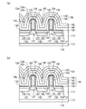
第1実施形態による半導体装置の製造方法を図1乃至図5を用いて説明する。図1乃至図4は、本実施形態による半導体装置の製造方法を示す工程断面図である。
[First Embodiment]
A method of manufacturing the semiconductor device according to the first embodiment will be described with reference to FIGS. 1 to 4 are process cross-sectional views illustrating the method for fabricating the semiconductor device according to the present embodiment.
まず、例えばSTI法により、素子領域を確定する素子分離領域14を半導体基板10に形成する(図1(a)参照)。半導体基板10としては、例えばシリコン基板を用いる。素子分離領域14の材料としては、例えばシリコン酸化膜を用いる。
First, an
次に、例えばイオン注入法により、P型のドーパント不純物を導入することにより、半導体基板10内にP型ウェル16を形成する。P型のドーパント不純物としては、例えばB(ボロン)を用いる。加速電圧は、例えば100〜200keVとする。ドーズ量は、例えば1×10¹³〜5×1013cm−2とする。
Next, a P-
次に、全面に、例えば熱酸化法により、例えば膜厚2〜5nmのシリコン酸化膜のゲート絶縁膜18を形成する。
Next, a
次に、全面に、例えばCVD法により、例えば膜厚50〜150nmのポリシリコン膜を形成する。 Next, a polysilicon film having a film thickness of, for example, 50 to 150 nm is formed on the entire surface by, eg, CVD.
次に、フォトリソグラフィ技術を用い、ポリシリコン膜をゲート電極20の形状にパターニングする。ゲート電極20のラインアンドスペース(L/S)は、例えば以下の通りとする。ライン(L)、即ち、ゲート配線20の幅は、例えば20〜90nmとする。スペース(S)、即ち、互いに隣接するゲート配線20とゲート配線20との間隔は、例えば50〜200nmとする。こうして、NMOSトランジスタ36(図2(c)参照)のゲート電極20が形成される(図1(b)参照)。
Next, the polysilicon film is patterned into the shape of the
次に、ゲート電極20をマスクとして、例えばイオン注入法により、ゲート電極20の両側の半導体基板10内にN型のドーパント不純物を導入する。N型のドーパント不純物としては、例えばAs(砒素)を用いる。加速電圧は、例えば5〜10keVとする。ドーズ量は、例えば5×10¹⁴〜10×1014cm−2とする。これにより、エクステンションソース/ドレイン構造の浅い領域を形成するエクステンション領域22が形成される(図1(c)参照)。
Next, using the
次に、全面に、例えばCVD法により、例えば膜厚5〜10nmのシリコン窒化膜24を形成する。
Next, a
次に、例えばRIE(Reactive Ion Etching、反応性イオンエッチング)法により、シリコン窒化膜24を異方性エッチングする。
Next, the
次に、全面に、例えばCVD法により、例えば膜厚20〜50nmのシリコン窒化膜26を形成する。
Next, a
次に、例えばRIE法により、シリコン窒化膜26を異方性エッチングする。これにより、ゲート電極20の側壁部分に、シリコン窒化膜24とシリコン窒化膜26との積層構造のサイドウォール絶縁膜28が形成される(図2(a)参照)。
Next, the
次に、ゲート電極20及びサイドウォール絶縁膜28をマスクとして、例えばイオン注入法により、ゲート電極20及びサイドウォール絶縁膜28の両側の半導体基板10内にN型のドーパント不純物を導入する。N型のドーパント不純物としては、例えばP(リン)を用いる。加速電圧は、例えば10〜20keVとする。ドーズ量は、例えば3×10¹³〜7×1013cm−2とする。これにより、エクステンションソース/ドレイン構造の深い領域を形成する不純物拡散領域30が形成される。エクステンション領域22と不純物拡散領域30とにより、エクステンションソース/ドレイン構造のソース/ドレイン拡散層32が形成される(図2(b)参照)。
Next, N-type dopant impurities are introduced into the
次に、全面に、例えばスパッタリング法により、膜厚10〜30nmの金属膜(図示せず)を形成する。かかる金属膜としては、例えばニッケル膜等を形成する。また、金属膜として、Pt等を添加したニッケル合金膜を形成してもよい。 Next, a 10-30 nm-thick metal film (not shown) is formed on the entire surface by, eg, sputtering. As such a metal film, for example, a nickel film or the like is formed. Further, a nickel alloy film to which Pt or the like is added may be formed as the metal film.
次に、例えばRTA(Rapid Thermal Annealing、短時間アニール)法により、ソース/ドレイン拡散層32の上部及びゲート電極20の上部をシリサイド化するための熱処理を行う。熱処理温度は、例えば200〜300℃とする。熱処理時間は、例えば10〜60秒とする。
Next, heat treatment for silicidizing the upper portion of the source /
次に、ウエットエッチングにより、高融点金属膜のうちの未反応の部分を除去する。エッチング液としては、例えば硫酸過水水溶液を用いる。 Next, an unreacted portion of the refractory metal film is removed by wet etching. As the etching solution, for example, an aqueous sulfuric acid / hydrogen peroxide solution is used.
次に、例えばRTA法により、熱処理を行う。熱処理温度は、例えば300〜400℃とする。熱処理時間は、例えば10〜120秒とする。 Next, heat treatment is performed by, for example, the RTA method. The heat treatment temperature is, for example, 300 to 400 ° C. The heat treatment time is, for example, 10 to 120 seconds.
こうして、ソース/ドレイン拡散層32上及びゲート電極20の上部にシリサイド膜34が形成される。ソース/ドレイン拡散層32上のシリサイド膜34は、ソース/ドレイン電極として機能する。
Thus, the
こうして、ゲート電極20とソース/ドレイン拡散層32とを有するNMOSトランジスタ36が形成される(図2(c)参照)。
Thus, the
次に、全面に、例えばCVD法により、1層目のシリコン窒化膜38を形成する(図3(a)参照)。より具体的には、プラズマCVD法により、シリコン窒化膜38を形成する。シリコン窒化膜38は、トランジスタ36のチャネル領域37に引張応力を印加する引張応力膜として機能するものである。1層目のシリコン窒化膜38は、後工程において形成される2層目のシリコン窒化膜40、3層目のシリコン窒化膜42及び4層目のシリコン窒化膜44と相俟って、トランジスタ36のチャネル領域37に引張応力を印加する。1層目のシリコン窒化膜38及び後工程で形成されるシリコン窒化膜40、42、44は、シリコン窒化膜38,40,42,44の積層膜により形成される引張応力膜の一部、即ち、部分膜である。シリコン窒化膜38の膜厚は、例えば10〜90nm程度とする。成膜室内には、例えばSiH4ガスとNH3ガスとN2ガスとを導入する。SiH4ガスの流量は、例えば20〜80sccm程度とする。NH3ガスの流量は、例えば500〜1300sccm程度とする。ここでは、NH3ガスの流量を例えば900sccm程度とする。N2ガスの流量は、例えば600〜1300sccm程度とする。成膜室内の圧力は、例えば2〜14Torr程度とする。基板温度は、例えば200〜500℃程度とする。印加する高周波電力は、例えば50〜200W程度とする。成膜時間は、例えば50〜150秒程度とする。
Next, a first
次に、エッチャントとなるNH4F(フッ化アンモニウム)ラジカルを、シャワーヘッド52を介してシリコン窒化膜38に供給する(図3(b)参照)。
Next, NH 4 F (ammonium fluoride) radical serving as an etchant is supplied to the
図5は、シリコン窒化膜にNH4Fラジカルを供給する際に用いられる装置の一部を示す図である。かかる装置としては、半導体製造ライン(図示せず)に設けられているドライクリーニング装置等の反応室(チャンバ)等を用いることができる。 FIG. 5 is a diagram showing a part of an apparatus used when supplying NH 4 F radicals to the silicon nitride film. As such an apparatus, a reaction chamber (chamber) such as a dry cleaning apparatus provided in a semiconductor production line (not shown) can be used.
半導体基板10が配置される反応室内には、半導体ウェハ10を支持するステージ46が設けられている。ステージ46には、半導体ウェハ10を支持するリフトピン48が設けられている。ステージ46は、半導体基板10を昇降させることが可能である。
A
ステージ46の上方には、シャワープレート50を有するシャワーヘッド52が設けられている。シャワーヘッド52には、シャワープレート50を加熱するヒータ54が設けられている。シャワーヘッド52は、気体を加熱して噴出することができる。
A
シャワーヘッド52の上流側には、プラズマ室(リモートプラズマ室)56が設けられている。プラズマ室56は、半導体ウェハ10から離間している。プラズマ室56では、プラズマ室56内に導入されるガスが高周波によりプラズマ化され、ラジカルが生成される。
A plasma chamber (remote plasma chamber) 56 is provided on the upstream side of the
プラズマ室56において印加される高周波電力は、例えば50W程度とする。プラズマ室56内には、例えば、NF3(三フッ化窒素)ガスとNH3(アンモニア)ガスとHeガスとが導入される。NF3ガスとNH3ガスはプロセスガスであり、Heガスは希釈ガスである。NF3ガスの流量は、例えば5〜30sccm程度とする。NH3ガスの流量は、例えば50〜100sccm程度とする。Heガスの流量は、例えば200〜400sccm程度とする。ここでは、Heガスの流量を300sccm程度とする。NF3ガス及びNH3ガスをプラズマ室56内に導入すると、NH4F(フッ化アンモニウム)ラジカル等が生成される。生成されたNH4Fラジカル等は、プラズマ室56の下流側に設けられたシャワーヘッド52を介して、半導体基板10上のシリコン窒化膜38に供給される。シリコン窒化膜38に供給されたNH4Fラジカル等は、シリコン窒化膜38のエッチャントとして機能する。シリコン窒化膜38にNH4Fラジカルを供給する際におけるシャワープレート54の温度は、例えば180℃程度とする。
The high frequency power applied in the
半導体基板10が載置される反応室内の圧力は、例えば1〜6Torr程度とする。半導体基板10に印加する高周波電力は、例えば10〜70W程度とする。
The pressure in the reaction chamber on which the
半導体基板10の温度が比較的高温に設定されている状態でシリコン窒化膜38にエッチャント(NH4Fラジカル)を供給した場合には、シリコン窒化膜38に供給されたエッチャントが昇華してしまい、シリコン窒化膜38を十分にエッチングし得ない。従って、シリコン窒化膜38にエッチャントを供給する際における半導体基板10の温度は、エッチャントが昇華しない程度の温度に設定することが好ましい。ここでは、半導体基板10の温度を例えば20〜40℃に設定する。
When an etchant (NH 4 F radical) is supplied to the
なお、シリコン窒化膜38にエッチャントを供給する際における半導体基板10の温度は、35℃に限定されるものではない。エッチャントが昇華しない程度の温度に半導体基板10の温度を設定すればよい。エッチャントが昇華しない程度の温度としては、例えば室温〜100℃とすることができる。
Note that the temperature of the
図3(b)に示すように、互いに隣接するゲート電極20とゲート電極20との間隔は比較的狭い。このため、シリコン窒化膜38のうちのゲート電極20間に位置する部分には、エッチャントとなるNH4Fラジカルが供給されにくい。
As shown in FIG. 3B, the interval between the
一方、シリコン窒化膜38のうちのゲート電極20間に位置する部分を除く部分においては、エッチャントとなるNH4Fラジカルが供給されやすい。
On the other hand, NH 4 F radicals serving as an etchant are easily supplied to a portion of the
図3(b)では、シリコン窒化膜38に供給されるエッチャントの供給量の分布を、丸印を用いて概念的に示している。
In FIG. 3B, the distribution of the supply amount of the etchant supplied to the
図3(b)に示すように、シリコン窒化膜38のうちのゲート電極20間に位置する部分を除く部分に供給されるエッチャントは比較的多い。
As shown in FIG. 3B, a relatively large amount of etchant is supplied to the portion of the
一方、シリコン窒化膜38のうちのゲート電極20間に位置する部分に供給されるエッチャントは比較的少ない。
On the other hand, the etchant supplied to the portion of the
シリコン窒化膜38にNH4Fラジカルが供給されると、NH4FラジカルがSiNと反応して、フッ化物が生成されると考えられる。かかるフッ化物は、(NH4)2SiNF6等であると考えられる。
When NH 4 F radicals are supplied to the
シリコン窒化膜38のうちのゲート電極20間に位置する部分を除く部分においては、エッチャントが比較的多く供給されるため、当該部分におけるシリコン窒化膜38のエッチング量は比較的大きくなる。
In a portion of the
一方、シリコン窒化膜38のうちのゲート電極20間に位置する部分においては、供給されるエッチャントが比較的少ないため、当該部分におけるシリコン窒化膜38のエッチング量は比較的小さくなる。
On the other hand, in the portion located between the
シリコン窒化膜38にエッチャントを供給する時間、即ち、エッチング時間は、例えば20〜60秒程度とする。
The time for supplying the etchant to the
次に、シリコン窒化膜38に対して熱処理(アニール)を行う。具体的には、図5(b)に示すように、半導体基板10を支持するステージ46を上昇させることにより、半導体基板10とシャワーヘッド52とを近接させる。シャワーヘッド52と半導体基板10とを近接させる際におけるシャワープレート54の温度は、例えば180℃程度とする。この際、シャワーヘッド52を介してシリコン窒化膜38にH2ガスを噴射する。加熱されたシャワーヘッド52にシリコン窒化膜38を近接させ、しかも、シャワーヘッド52により加熱されたH2ガスがシリコン窒化膜38に供給されるため、シリコン窒化膜38が速やかに加熱される。シリコン窒化膜38を例えば100℃以上に加熱すると、エッチャントとSiNとが反応することにより生成されたフッ化物等が昇華して、SiF4ガスやNH3ガス等となる。エッチャントとSiNとが反応してフッ化物等となった部分が、この熱処理により昇華除去され、シリコン窒化膜38がエッチバックされることとなる。このようにして、シリコン窒化膜38は、ゲート電極20上において、例えば5〜40nm程度エッチングされることとなる。
Next, heat treatment (annealing) is performed on the
シリコン窒化膜38のうちのゲート電極20間に位置する部分を除く部分は、フッ化物等が比較的多く生成されていたため、シリコン窒化膜38の表層部が比較的大きく除去される。
Since a relatively large amount of fluoride or the like is generated in the portion of the
一方、シリコン窒化膜38のうちのゲート電極20間に位置する部分は、生成されていたフッ化物等が比較的少ないため、シリコン窒化膜38の表層部の除去量は比較的少ない。
On the other hand, the portion of the
従って、シリコン窒化膜38のうちのゲート電極20間に位置する部分を除く部分においては、図3(c)に示すように、残存するシリコン窒化膜38の膜厚が比較的薄い。
Therefore, in the portion of the
一方、シリコン窒化膜38のうちのゲート電極20間に位置する部分においては、図3(c)に示すように、シリコン窒化膜38が比較的厚く残存する。
On the other hand, in the portion of the
ゲート電極20が互いに隣接している箇所においては、ソース/ドレイン拡散層32上からゲート電極20上に向かってシリコン窒化膜38の膜厚が徐々に薄くなるように、シリコン窒化膜38が残存する。
In locations where the
このため、ゲート電極20が互いに隣接している箇所においては、シリコン窒化膜38の表面の傾斜が比較的緩やかになる。このことは、後工程においてシリコン窒化膜40、42、44を形成する際に、互いに隣接するゲート電極20間において鬆が生じるのを防止することに寄与する。
For this reason, the slope of the surface of the
こうして、シリコン窒化膜38がエッチバックされることとなる。エッチバック後のシリコン窒化膜38のゲート電極20上における膜厚は、例えば10〜40nm程度となる。
Thus, the
なお、シリコン窒化膜38のうちのゲート絶縁膜20上の部分の膜厚が過度に薄くなった場合には、NMOSトランジスタ36のチャネル領域37に十分な引張応力を加えることができなくなる。このため、シリコン窒化膜38のうちのゲート絶縁膜20上の部分の膜厚を、過度に薄くしないことが好ましい。具体的には、エッチバック後のシリコン窒化膜38のゲート絶縁膜20上における膜厚は、例えば5〜15nm以上とすることが好ましい。
If the thickness of the portion of the
次に、シリコン窒化膜38に対して紫外線キュア(UVキュア)を行う。紫外線キュアを行う際におけるチャンバ内の雰囲気は、例えばヘリウム雰囲気とする。ヘリウムガスの流量は、例えば7000〜12000sccm程度とする。チャンバ内の圧力は、例えば2.0〜14Torr程度とする。紫外線ランプのパワーは、例えば20〜180W程度とする。ここでは、紫外線ランプのパワーを100W程度とする。半導体基板10の温度は、例えば300〜500℃程度とする。紫外線キュアの時間は、例えば1〜20分程度とする。ここでは、紫外線キュアの時間を例えば5分程度とする。紫外線キュア後のシリコン窒化膜38のゲート電極20上における膜厚は、例えば10〜40nm程度となる。
Next, ultraviolet curing (UV curing) is performed on the
次に、図3(a)を用いて上述したシリコン窒化膜38の形成方法と同様にして、2層目のシリコン窒化膜40を形成する(図4(a)参照)。シリコン窒化膜40の膜厚は、例えば30〜60nmとする。上記のようにエッチバックされたシリコン窒化膜38上にシリコン窒化膜40を形成するため、シリコン窒化膜40に鬆が形成されることはない。
Next, a second
次に、上述したシリコン窒化膜38に対する紫外線キュアと同様にして、シリコン窒化膜40に対して紫外線キュアを行う。紫外線キュア後のシリコン窒化膜40のゲート電極20上における膜厚は、例えば10〜50nm程度となる。
Next, ultraviolet curing is performed on the
次に、図3(a)を用いて上述したシリコン窒化膜38の形成方法と同様にして、3層目のシリコン窒化膜42を形成する(図4(b)参照)。シリコン窒化膜42の膜厚は、例えば30〜60nmとする。上記のようにエッチバックされたシリコン窒化膜38上にシリコン窒化膜40、42を積層するため、シリコン窒化膜42に鬆が形成されることはない。
Next, in the same manner as the method for forming the
次に、上述したシリコン窒化膜38に対する紫外線キュアと同様にして、シリコン窒化膜42に対して紫外線キュアを行う。紫外線キュア後のシリコン窒化膜42のゲート電極20上における膜厚は、例えば10〜50nm程度となる。
Next, ultraviolet curing is performed on the
次に、図3(a)を用いて上述したシリコン窒化膜38の形成方法と同様にして、4層目のシリコン窒化膜44を形成する(図4(c)参照)。シリコン窒化膜44の膜厚は、例えば30〜60nmとする。上記のようにエッチバックされたシリコン窒化膜38上にシリコン窒化膜40、42、44を積層するため、シリコン窒化膜44に鬆が形成されることはない。
Next, a fourth
次に、上述したシリコン窒化膜38に対する紫外線キュアと同様にして、シリコン窒化膜44に対して紫外線キュアを行う。紫外線キュア後のシリコン窒化膜44のゲート電極20上における膜厚は、例えば10〜50nm程度となる。シリコン窒化膜38,40,42,44のゲート電極20上における総膜厚は、例えば50〜100nm程度となる。
Next, ultraviolet curing is performed on the
こうして、シリコン窒化膜38,40,42,44の積層膜により形成された引張応力膜45が、NMOSトランジスタ36を覆うように形成される。
Thus, the
こうして、本実施形態による半導体装置が製造される。 Thus, the semiconductor device according to the present embodiment is manufactured.
(評価結果)
次に、本実施形態による半導体装置の製造方法の評価結果について図6乃至図9を用いて説明する。
(Evaluation results)
Next, evaluation results of the semiconductor device manufacturing method according to the present embodiment will be explained with reference to FIGS.
図6は、シリコン窒化膜の膜ストレスを示すグラフである。図6において、実施例1は、本実施形態の場合、即ち、シリコン窒化膜38にNH4Fラジカルを供給し、この後、シリコン窒化膜38に対して熱処理を行うことにより、シリコン窒化膜38をエッチバックする場合を示している。図6において、比較例1は、シリコン窒化膜に対してAr(アルゴン)の高密度プラズマ(HDP、High Density Plasma)を照射することにより、シリコン窒化膜をエッチバックする場合を示している。図6において、「成膜直後」は、シリコン窒化膜を成膜した直後におけるシリコン窒化膜の膜ストレスを示している。成膜直後のシリコン窒化膜の膜厚は、40nmとした。図6において、「エッチバック後」は、エッチバック後におけるシリコン窒化膜の膜ストレスを示している。エッチバック後のシリコン窒化膜のゲート電極上における膜厚は、30nmとした。
FIG. 6 is a graph showing the film stress of the silicon nitride film. In FIG. 6, Example 1 is the case of the present embodiment, that is, by supplying NH 4 F radicals to the
図6から分かるように、比較例1の場合には、シリコン窒化膜の膜ストレスが25%程度も低下してしまう。 As can be seen from FIG. 6, in the case of Comparative Example 1, the film stress of the silicon nitride film is reduced by about 25%.
これに対し、実施例1の場合には、シリコン窒化膜の膜ストレスの低下はわずか4%程度である。 On the other hand, in the case of Example 1, the decrease in the film stress of the silicon nitride film is only about 4%.
このことから、本実施形態によれば、シリコン窒化膜の膜ストレスの著しい低下を招くことなく、シリコン窒化膜をエッチバックし得ることができることが分かる。本実施形態によれば、トランジスタのチャネル領域に所望のストレスを印加し得るため、移動度の高い、電気的特性の良好なトランジスタを得ることができる。 From this, it can be seen that according to the present embodiment, the silicon nitride film can be etched back without causing a significant decrease in the film stress of the silicon nitride film. According to this embodiment, since a desired stress can be applied to the channel region of the transistor, a transistor with high mobility and good electrical characteristics can be obtained.
図7は、エッチング時間とエッチングレートとの関係を示すグラフである。図7における横軸は、エッチング時間、即ち、シリコン窒化膜にNH4Fラジカルを供給する時間を示している。図7における縦軸は、シリコン窒化膜のエッチングレートを示している。 FIG. 7 is a graph showing the relationship between the etching time and the etching rate. The horizontal axis in FIG. 7 shows the etching time, that is, the time for supplying NH 4 F radicals to the silicon nitride film. The vertical axis in FIG. 7 indicates the etching rate of the silicon nitride film.
図7から分かるように、エッチング時間が長くなるに伴って、シリコン窒化膜のエッチングレートが遅くなる。 As can be seen from FIG. 7, the etching rate of the silicon nitride film becomes slower as the etching time becomes longer.
図8は、エッチング時間とエッチング量との関係を示すグラフである。図8における横軸は、エッチング時間、即ち、シリコン窒化膜にNH4Fラジカルを供給する時間を示している。図8における縦軸は、シリコン窒化膜のエッチング量を示している。 FIG. 8 is a graph showing the relationship between the etching time and the etching amount. The horizontal axis in FIG. 8 represents the etching time, that is, the time for supplying NH 4 F radicals to the silicon nitride film. The vertical axis in FIG. 8 indicates the etching amount of the silicon nitride film.
図8から分かるように、シリコン窒化膜のエッチング量はエッチング時間に依存するが、エッチング時間が長くなるに伴ってエッチングレートが低下する傾向にある。 As can be seen from FIG. 8, the etching amount of the silicon nitride film depends on the etching time, but the etching rate tends to decrease as the etching time becomes longer.
図9は、エッチング時間とエッチング量の面内ばらつきとの関係を示すグラフである。図9における横軸は、エッチング時間、即ち、シリコン窒化膜にNH4Fラジカルを供給する時間を示している。図9における縦軸は、エッチング量の面内ばらつき、より具体的には、エッチング量の最大値と最小値との差を示している。 FIG. 9 is a graph showing the relationship between the etching time and the in-plane variation of the etching amount. The horizontal axis in FIG. 9 indicates the etching time, that is, the time for supplying NH 4 F radicals to the silicon nitride film. The vertical axis in FIG. 9 indicates the in-plane variation of the etching amount, more specifically, the difference between the maximum value and the minimum value of the etching amount.
図9に示すように、エッチング時間が長くなるに伴って、エッチング量の面内ばらつきは大きくなる傾向にある。 As shown in FIG. 9, the in-plane variation of the etching amount tends to increase as the etching time becomes longer.
エッチング量の面内ばらつきは、10nm以下となるようにすることが好ましい。従って、エッチング時間は、90秒以下とすることが好ましい。 The in-plane variation in the etching amount is preferably 10 nm or less. Therefore, the etching time is preferably 90 seconds or less.
このように本実施形態によれば、シリコン窒化膜38にエッチャントとなるNH4Fラジカルを供給し、この後、シリコン窒化膜38に対して熱処理を行うことにより、シリコン窒化膜38をエッチバックする。シリコン窒化膜38のうちのゲート電極20間に位置する部分においては、供給されるエッチャントが比較的少ないため、シリコン窒化膜38のエッチング量は比較的小さくなる。一方、シリコン窒化膜38のうちのゲート電極20間に位置する部分を除く部分においては、エッチャントが比較的多く供給されるため、シリコン窒化膜38は比較的大きくエッチングされる。このため、本実施形態によれば、ゲート電極20間に位置するソース/ドレイン拡散層32上からゲート電極20上に向かってシリコン窒化膜38の膜厚が徐々に薄くなるように、シリコン窒化膜38が残存する。このため、本実施形態によれば、ゲート電極20が互いに隣接している箇所において、シリコン窒化膜38の表面の傾斜が比較的緩やかになる。このようにエッチバックされたシリコン窒化膜38上にシリコン窒化膜40、42、44を形成するため、本実施形態によれば、シリコン窒化膜38、40、42、44の積層膜45に鬆が生じるのを防止することができる。従って、本実施形態によれば、信頼性の高い半導体装置を高い歩留まりで提供することができる。
As described above, according to the present embodiment, NH 4 F radicals serving as an etchant are supplied to the
(変形例)
次に、本実施形態の変形例による半導体装置の製造方法を図10乃至図12を用いて説明する。図10乃至図12は、本実施形態による半導体装置の製造方法を示す工程断面図である。
(Modification)
Next, a method for manufacturing a semiconductor device according to a modification of the present embodiment will be described with reference to FIGS. 10 to 12 are process cross-sectional views illustrating the method for fabricating the semiconductor device according to the present embodiment.
本実施形態による半導体装置の製造方法は、シリコン窒化膜38のエッチバックを2回に分けて行うことに主な特徴がある。
The semiconductor device manufacturing method according to the present embodiment is mainly characterized in that the
まず、素子分離領域14を形成する工程からシリコン窒化膜38を形成する工程までは、図1(a)乃至図3(a)に示す第1実施形態による半導体装置の製造方法と同様であるので、説明を省略する(図10(a)参照)。
First, the process from the formation of the
次に、図3(b)を用いて上述した第1実施形態による半導体装置の製造方法と同様にして、エッチャントとなるNH4Fラジカルをシリコン窒化膜38に供給する(図10(b)参照)。本実施形態では、2回に分けてシリコン窒化膜38をエッチバックするため、1回分のエッチング時間は、第1実施形態の場合の半分程度とすればよい。ここでは、1回目のエッチングにおけるエッチング時間を、例えば10〜30秒とする。エッチング時間以外のエッチング条件については、図3(b)を用いて上述したシリコン窒化膜38のエッチング条件と同様とする。
Next, in the same manner as in the method of manufacturing the semiconductor device according to the first embodiment described above with reference to FIG. 3B, NH 4 F radicals serving as an etchant are supplied to the silicon nitride film 38 (see FIG. 10B). ). In this embodiment, since the
次に、図3(c)を用いて上述した第1実施形態による半導体装置の製造方法と同様にして、シリコン窒化膜38に対して熱処理を行う(図10(c)参照)。シリコン窒化膜38のうちのゲート電極20間に位置する部分においては、供給されるエッチャントが比較的少ないため、シリコン窒化膜38のエッチング量は比較的小さくなる。一方、シリコン窒化膜38のうちのゲート電極20間に位置する部分を除く部分においては、エッチャントが比較的多く供給されるため、シリコン窒化膜38は比較的大きくエッチングされる。このため、ゲート電極20間に位置するソース/ドレイン拡散層32上からゲート電極20上に向かってシリコン窒化膜38の膜厚が徐々に薄くなるように、シリコン窒化膜38が残存する。このため、ゲート電極20が互いに隣接している箇所において、シリコン窒化膜38の表面の傾斜が比較的緩やかになる。
Next, heat treatment is performed on the
こうして、シリコン窒化膜38に対しての1回目のエッチバックが行われる。こうしてエッチバックを行うと、シリコン窒化膜38は、ゲート電極20上の部分において、例えば5〜35nm程度エッチバックされる。1回目のエッチバック後のシリコン窒化膜38のゲート電極20上における膜厚は、例えば10〜40nm程度とする。
Thus, the first etch back is performed on the
次に、図3(b)を用いて上述した第1実施形態による半導体装置の製造方法と同様にして、エッチャントとなるNH4Fラジカルをシリコン窒化膜38に供給する(図11(a)参照)。上述したように、本実施形態では、2回に分けてシリコン窒化膜38をエッチバックするため、1回分のエッチング時間は、第1実施形態の場合の半分程度とすればよい。ここでは、2回目のエッチングにおけるエッチング時間を、例えば10〜30秒とする。エッチング時間以外のエッチング条件については、図3(b)を用いて上述したシリコン窒化膜38のエッチング条件と同様とする。
Next, in the same manner as in the method of manufacturing the semiconductor device according to the first embodiment described above with reference to FIG. 3B, NH 4 F radicals serving as an etchant are supplied to the silicon nitride film 38 (see FIG. 11A). ). As described above, in this embodiment, since the
次に、図3(c)を用いて上述した第1実施形態による半導体装置の製造方法と同様にして、シリコン窒化膜38に対して熱処理を行う(図11(b)参照)。シリコン窒化膜38のうちのゲート電極20間に位置する部分においては、供給されるエッチャントが比較的少ないため、シリコン窒化膜38のエッチング量は比較的小さくなる。一方、シリコン窒化膜38のうちのゲート電極20間に位置する部分を除く部分においては、エッチャントが比較的多く供給されるため、シリコン窒化膜38は比較的大きくエッチングされる。このため、ゲート電極20間に位置するソース/ドレイン拡散層32上からゲート電極20上に向かってシリコン窒化膜38の膜厚が徐々に薄くなるように、シリコン窒化膜38が残存する。このため、ゲート電極20が互いに隣接している箇所において、シリコン窒化膜38の表面の傾斜が比較的緩やかになる。このことは、後工程においてシリコン窒化膜40、42、44を形成する際に、互いに隣接するゲート電極20間において鬆が生じるのを防止することに寄与する。
Next, heat treatment is performed on the
こうして、シリコン窒化膜38に対しての2回目のエッチバックが行われる。こうしてエッチバックを行うと、シリコン窒化膜38は、ゲート電極20上の部分において、例えば5〜35nm程度エッチバックされる。2回目のエッチバック後のシリコン窒化膜38のゲート電極20上における膜厚は、例えば10〜40nm程度とする。
Thus, the second etch back is performed on the
次に、図3(c)を用いて上述した第1実施形態による半導体装置の製造方法と同様にして、シリコン窒化膜38に対して紫外線キュアを行う。紫外線キュア後のシリコン窒化膜38のゲート電極20上における膜厚は、例えば10〜40nm程度とする。
Next, ultraviolet curing is performed on the
こうして、シリコン窒化膜38に対するエッチバックが2回に分けて行われる。
Thus, the etch back for the
この後の半導体装置の製造方法は、図4(a)乃至図4(c)を用いて上述した第1実施形態による半導体装置の製造方法と同様であるので、説明を省略する(図11(c)乃至図12(b)参照)。 The subsequent manufacturing method of the semiconductor device is the same as the manufacturing method of the semiconductor device according to the first embodiment described above with reference to FIGS. c) thru | or FIG.12 (b)).
このように、シリコン窒化膜38に対するエッチバックを2回に分けて行ってもよい。
Thus, the etch back for the
[第2実施形態]
第2実施形態による半導体装置の製造方法を図13乃至図15を用いて説明する。図13乃至図15は、本実施形態による半導体装置の製造方法を示す工程断面図である。図1乃至図12に示す第1実施形態による半導体装置の製造方法と同一の構成要素には、同一の符号を付して説明を省略または簡潔にする。
[Second Embodiment]
A method for fabricating a semiconductor device according to the second embodiment will be described with reference to FIGS. 13 to 15 are process cross-sectional views illustrating the method for fabricating the semiconductor device according to the present embodiment. The same components as those in the semiconductor device manufacturing method according to the first embodiment shown in FIGS. 1 to 12 are denoted by the same reference numerals, and description thereof will be omitted or simplified.
本実施形態による半導体装置の製造方法は、1層目のシリコン窒化膜38のみならず、2層目のシリコン窒化膜40に対してもNH4Fラジカルを用いてエッチバックを行うことに主な特徴がある。
The manufacturing method of the semiconductor device according to the present embodiment is mainly performed to etch back not only the first
まず、半導体基板10に素子分離領域14を形成する工程からシリコン窒化膜40を形成する工程までは、図1(a)乃至4(a)を用いて上述した第1実施形態による半導体装置の製造方法と同様であるので、説明を省略する(図13(a)乃至図14(a)参照)。
First, from the step of forming the
次に、図3(b)を用いて上述した第1実施形態による半導体装置の製造方法と同様にして、エッチャントとなるNH4Fラジカルをシリコン窒化膜40に供給する(図14(b)参照)。 Next, in the same manner as in the method of manufacturing the semiconductor device according to the first embodiment described above with reference to FIG. 3B, NH 4 F radicals serving as an etchant are supplied to the silicon nitride film 40 (see FIG. 14B). ).
次に、図3(c)を用いて上述した第1実施形態による半導体装置の製造方法と同様にして、シリコン窒化膜40に対して熱処理を行うことにより、シリコン窒化膜40をエッチバックする(図14(c)参照)。シリコン窒化膜40のうちのゲート電極20間に位置する部分においては、供給されるエッチャントが比較的少ないため、シリコン窒化膜40のエッチング量は比較的小さくなる。一方、シリコン窒化膜40のうちのゲート電極20間に位置する部分を除く部分においては、エッチャントが比較的多く供給されるため、シリコン窒化膜40は比較的大きくエッチングされる。このため、ゲート電極20間に位置するソース/ドレイン拡散層32上からゲート電極20上に向かってシリコン窒化膜40の膜厚が徐々に薄くなるように、シリコン窒化膜40が残存する。このため、ゲート電極20が互いに隣接している箇所において、シリコン窒化膜40の表面の傾斜が比較的緩やかになる。このことは、後工程においてシリコン窒化膜42、44を形成する際に、互いに隣接するゲート電極20間において鬆が生じるのを防止することに寄与する。また、シリコン窒化膜40をこのようにエッチバックするため、シリコン窒化膜40自体に鬆が生じることもない。
Next, the
こうしてエッチバックを行うと、シリコン窒化膜40は、ゲート電極20上の部分において、例えば10〜40nm程度エッチバックされる。熱処理後におけるシリコン窒化膜40のゲート電極20上における膜厚は、例えば10〜40nm程度となる。
When etch back is performed in this manner, the
なお、シリコン窒化膜40のうちのゲート絶縁膜20上の部分の膜厚が過度に薄くなった場合には、NMOSトランジスタ36のチャネル領域37に十分な引張応力を加えることができなくなる。このため、シリコン窒化膜40のうちのゲート絶縁膜20上の部分の膜厚を、過度に薄くしないことが好ましい。具体的には、エッチバック後のシリコン窒化膜40のゲート絶縁膜20上における膜厚は、例えば5〜15nm以上とすることが好ましい。
If the thickness of the
次に、図3(c)を用いて上述した第1実施形態による半導体装置の製造方法と同様にして、シリコン窒化膜40に対して紫外線キュアを行う。紫外線キュア後のシリコン窒化膜40のゲート電極20上における膜厚は、例えば10〜40nm程度となる。
Next, ultraviolet curing is performed on the
この後の半導体装置の製造方法は、図4(b)及び図4(c)を用いて上述した第1実施形態による半導体装置の製造方法と同様であるため、説明を省略する(図15(a)及び図15(b)参照)。 The subsequent method for manufacturing the semiconductor device is the same as the method for manufacturing the semiconductor device according to the first embodiment described above with reference to FIGS. a) and FIG. 15B).
このように、1層目のシリコン窒化膜38のみならず、2層目のシリコン窒化膜40に対してもNH4Fラジカルを用いてエッチバックを行うようにしてもよい。
In this manner, not only the first
[第3実施形態]
第3実施形態による半導体装置の製造方法を図16乃至図19を用いて説明する。図16乃至図19は、本実施形態による半導体装置の製造方法を示す工程断面図である。図1乃至図15に示す第1又は第2実施形態による半導体装置の製造方法と同一の構成要素には、同一の符号を付して説明を省略または簡潔にする。
[Third Embodiment]
A method for fabricating a semiconductor device according to the third embodiment will be described with reference to FIGS. 16 to 19 are process cross-sectional views illustrating the method for fabricating the semiconductor device according to the present embodiment. The same components as those in the method of manufacturing the semiconductor device according to the first or second embodiment shown in FIGS. 1 to 15 are denoted by the same reference numerals, and description thereof is omitted or simplified.
本実施形態による半導体装置の製造方法は、1層目のシリコン窒化膜38及び2層目のシリコン窒化膜40のみならず、3層目のシリコン窒化膜42に対してもNH4Fラジカルを用いてエッチバックを行うことに主な特徴がある。
The manufacturing method of the semiconductor device according to the present embodiment uses NH 4 F radicals not only for the first
まず、半導体基板10に素子分離領域14を形成する工程からシリコン窒化膜40を形成する工程までは、図1(a)乃至4(a)を用いて上述した第1実施形態による半導体装置の製造方法と同様であるので、説明を省略する(図16(a)乃至図17(a)参照)。
First, from the step of forming the
次に、NH4Fラジカルをシリコン窒化膜40に供給する工程からシリコン窒化膜40に対して紫外線キュアを行う工程までは、図14(b)及び図14(c)を用いて上述した第2実施形態による半導体装置の製造方法と同様である。このため、NH4Fラジカルをシリコン窒化膜40に供給する工程からシリコン窒化膜40に対して紫外線キュアを行う工程までは、説明を省略する(図17(b)及び図17(c)参照)。
Next, from the step of supplying NH 4 F radicals to the
次に、図4(b)を用いて上述した第1実施形態による半導体装置の製造方法と同様にして、シリコン窒化膜42を形成する(図18(a)参照)。
Next, a
次に、図3(b)を用いて上述した第1実施形態による半導体装置の製造方法と同様にして、エッチャントとなるNH4Fラジカルをシリコン窒化膜42に供給する(図18(b)参照)。 Next, in the same manner as in the method of manufacturing the semiconductor device according to the first embodiment described above with reference to FIG. 3B, NH 4 F radicals serving as an etchant are supplied to the silicon nitride film 42 (see FIG. 18B). ).
次に、図3(c)を用いて上述した第1実施形態による半導体装置の製造方法と同様にして、シリコン窒化膜42に対して熱処理を行うことにより、シリコン窒化膜42をエッチバックする(図18(c)参照)。シリコン窒化膜42のうちのゲート電極20間に位置する部分においては、供給されるエッチャントが比較的少ないため、シリコン窒化膜42のエッチング量は比較的小さくなる。一方、シリコン窒化膜42のうちのゲート電極20間に位置する部分を除く部分においては、エッチャントが比較的多く供給されるため、シリコン窒化膜42は比較的大きくエッチングされる。このため、ゲート電極20間に位置するソース/ドレイン拡散層32上からゲート電極20上に向かってシリコン窒化膜42の膜厚が徐々に薄くなるように、シリコン窒化膜42が残存する。このため、ゲート電極20が互いに隣接している箇所において、シリコン窒化膜42の表面の傾斜が比較的緩やかになる。このことは、後工程においてシリコン窒化膜44を形成する際に、互いに隣接するゲート電極20間において鬆が生じるのを防止することに寄与する。また、シリコン窒化膜42をこのようにエッチバックするため、シリコン窒化膜42自体に鬆が生じることもない。
Next, the
こうしてエッチバックを行うと、シリコン窒化膜42は、ゲート電極20上の部分において、例えば10〜40nm程度エッチバックされる。エッチバック後におけるシリコン窒化膜42のゲート電極20上における膜厚は、例えば10〜40nm程度となる。
When etching back is performed in this way, the
なお、シリコン窒化膜42のうちのゲート絶縁膜20上の部分の膜厚が過度に薄くなった場合には、NMOSトランジスタ36のチャネル領域37に十分な引張応力を加えることができなくなる。このため、シリコン窒化膜42のうちのゲート絶縁膜20上の部分の膜厚を、過度に薄くしないことが好ましい。具体的には、エッチバック後のシリコン窒化膜42のゲート絶縁膜20上における膜厚は、例えば5〜15nm以上とすることが好ましい。
If the thickness of the
次に、図3(c)を用いて上述した第1実施形態による半導体装置の製造方法と同様にして、シリコン窒化膜42に対して紫外線キュアを行う。紫外線キュア後のシリコン窒化膜42のゲート電極20上における膜厚は、例えば10〜40nm程度となる。
Next, ultraviolet curing is performed on the
この後の半導体装置の製造方法は、図4(c)を用いて上述した第1実施形態による半導体装置の製造方法と同様であるため、説明を省略する(図19参照)。 The subsequent manufacturing method of the semiconductor device is the same as the manufacturing method of the semiconductor device according to the first embodiment described above with reference to FIG.
このように、1層目のシリコン窒化膜38及び2層目のシリコン窒化膜40のみならず、3層目のシリコン窒化膜42に対してもNH4Fラジカルを用いてエッチバックを行うようにしてもよい。
In this way, not only the first
[第4実施形態]
第4実施形態による半導体装置の製造方法を図20乃至図25を用いて説明する。図20乃至図25は、本実施形態による半導体装置の製造方法を示す工程断面図である。図1乃至図19に示す第1乃至第3実施形態による半導体装置の製造方法と同一の構成要素には、同一の符号を付して説明を省略または簡潔にする。
[Fourth Embodiment]
A method for fabricating a semiconductor device according to the fourth embodiment will be described with reference to FIGS. 20 to 25 are process cross-sectional views illustrating the method for fabricating the semiconductor device according to the present embodiment. The same components as those of the semiconductor device manufacturing method according to the first to third embodiments shown in FIGS. 1 to 19 are denoted by the same reference numerals, and description thereof will be omitted or simplified.
本実施形態による半導体装置の製造方法は、トランジスタ70がPMOSトランジスタであり、応力膜72、74、76、78が圧縮応力膜であることに主な特徴がある。
The semiconductor device manufacturing method according to the present embodiment is mainly characterized in that the
まず、図1(a)を用いて上述した第1実施形態による半導体装置の製造方法と同様にして、素子領域を確定する素子分離領域14を半導体基板10に形成する(図20(a)参照)。
First, in the same manner as in the semiconductor device manufacturing method according to the first embodiment described above with reference to FIG. 1A, an
次に、例えばイオン注入法により、N型のドーパント不純物を導入することにより、半導体基板10内にN型ウェル58を形成する。N型のドーパント不純物としては、例えばPを用いる。加速電圧は、例えば100〜500keVとする。ドーズ量は、例えば1×10¹³〜5×1013cm−2とする。
Next, an N-
次に、図1(b)を用いて上述した第1実施形態による半導体装置の製造方法と同様にして、ゲート絶縁膜18を形成する(図20(b)参照)。
Next, the
次に、図1(b)を用いて上述した第1実施形態による半導体装置の製造方法と同様にして、ゲート電極20を形成する。
Next, the
次に、ゲート電極20をマスクとして、例えばイオン注入法により、ゲート電極20の両側の半導体基板10内にP型のドーパント不純物を導入する。P型のドーパント不純物としては、例えばBを用いる。加速電圧は、例えば1〜5keVとする。ドーズ量は、例えば1×10¹⁵〜5×1015cm−2とする。これにより、エクステンションソース/ドレイン構造の浅い領域を形成するエクステンション領域60が形成される(図20(c)参照)。
Next, using the
次に、図2(a)を用いて上述した第1実施形態による半導体装置の製造方法と同様にして、サイドウォール絶縁膜28を形成する(図21(a)参照)。
Next, a
次に、ゲート電極20及びサイドウォール絶縁膜28をマスクとして、例えばイオン注入法により、ゲート電極20及びサイドウォール絶縁膜28の両側の半導体基板10内にP型のドーパント不純物を導入する。P型のドーパント不純物としては、例えばBを用いる。加速電圧は、例えば3〜7keVとする。ドーズ量は、例えば3×10¹⁵〜9×1015cm−2とする。これにより、エクステンションソース/ドレイン構造の深い領域を形成する不純物拡散領域62が形成される。エクステンション領域60と不純物拡散領域62とにより、エクステンションソース/ドレイン構造のソース/ドレイン拡散層64が形成される(図21(b)参照)。
Next, using the
なお、ここでは、後述するシリコンゲルマニウム層68を形成する前にソース/ドレイン拡散層64を形成する場合を例に説明したが、後述するシリコンゲルマニウム層68を形成した後に、ソース/ドレイン拡散層64を形成してもよい。
Here, the case where the source /
次に、例えばRIE法により、半導体基板10をエッチングする。エッチング条件は、例えば以下の通りとする。印加する高周波電力は、例えば100〜600W程度とする。チャンバ内に導入するガスは、O2ガス、Heガス、Arガス、CHF3ガス、SF6ガス、HBrガス、SiCl4ガス等を適宜用いる。チャンバ内の圧力は、例えば1〜20mTorr程度とする。エッチング時間は、例えば10〜60秒程度とする。基板温度は、例えば10〜150℃程度とする。これにより、ゲート電極20及びサイドウォール絶縁膜28の両側のソース/ドレイン拡散層64内に、凹部66が形成される(図21(c)参照)。
Next, the
次に、例えばウエットエッチングにより、半導体基板10をエッチングする(図22(a)参照)。エッチング液としては、例えば水酸化テトラメチルアンモニウム(TMAH)水溶液、水酸化ヒドロキシエチルトリメチルアンモニウム(コリン、CHOLINE)水溶液等の有機アルカリエッチャントを用いることができる。また、エッチング液として、水酸化アンモニウム等を用いてもよい。エッチング時間は、例えば10〜90秒程度とする。エッチング量は、例えば5〜25nm程度とする。このウエットエッチングにより、サイドウォール絶縁膜28の下方領域に達する切り込み部を含む凹部66が形成される。この際、ゲート電極20の上部もエッチングされるため、ゲート電極20上部にも凹部66が形成される。
Next, the
なお、ゲート電極20の上部に凹部66が形成されないようにしてもよい。
Note that the
次に、例えばバッチ式縦型炉を用い、凹部66内にシリコンゲルマニウム層68をエピタキシャル成長する。シリコンゲルマニウム層68の成長条件は、例えば以下の通りとする。原料ガスとしては、例えばH2ガス、SiH4ガス、GeH4ガス、HClガス等を用いる。炉内の温度は、例えば400〜600℃程度とする。処理時間は、例えば5〜10時間程度とする。
Next, the
次に、図2(c)を用いて上述した第1実施形態による半導体装置の製造方法と同様にして、シリサイド膜34を形成する。シリコンゲルマニウム層68上のシリサイド膜34は、ソース/ドレイン電極として機能する。
Next, a
こうして、ゲート電極20とソース/ドレイン拡散層64とを有するPMOSトランジスタ70が形成される(図22(c)参照)。
Thus, the
次に、全面に、例えばCVDにより、1層目のシリコン窒化膜72を形成する(図23(a)参照)。より具体的には、プラズマCVD法により、シリコン窒化膜72を形成する。シリコン窒化膜72は、トランジスタ70のチャネル領域71に圧縮応力を印加する圧縮応力膜として機能するものである。1層目のシリコン窒化膜72は、後工程において形成される2層目のシリコン窒化膜74、3層目のシリコン窒化膜76及び4層目のシリコン窒化膜78と相俟って、トランジスタ70のチャネル領域71に圧縮応力を印加する。1層目のシリコン窒化膜72及び後工程で形成されるシリコン窒化膜74、76、78は、シリコン窒化膜の積層膜により形成される圧縮応力膜の一部、即ち、部分膜である。シリコン窒化膜72の膜厚は、例えば10〜90nm程度とする。成膜室内には、例えばSiH4ガスとNH3ガスとを導入する。SiH4ガスの流量は、例えば20〜80sccm程度とする。NH3ガスの流量は、例えば80〜120sccm程度とする。成膜室内の圧力は、例えば1.0〜4.0Torr程度とする。ここでは、成膜室内の圧力を例えば2.0Torr程度とする。基板温度は、例えば300〜500℃程度とする。印加する低周波電力は、例えば10〜60W程度とする。印加する高周波電力は、例えば40〜140W程度とする。成膜時間は、例えば50〜150秒程度とする。
Next, a first
次に、シリコン窒化膜72に対して酸素(O2)プラズマ処理を行う(図23(b)参照)。酸素プラズマ処理は、シリコン窒化膜72のエッチングレートを向上するためのものである。圧縮応力膜72は、引張応力膜38と比較して硬質であり、エッチングレートが遅い。このため、圧縮応力膜72に対しては、酸素プラズマ処理を行うことが好ましい。酸素プラズマ処理の条件は以下の通りとする。チャンバ内に導入するガスは、例えば酸素ガスとアルゴン(Ar)ガスとする。酸素ガスの流量は、例えば10〜50sccm程度とする。Arガスの流量は、例えば50〜150sccm程度とする。印加する高周波電力は、例えば1000〜3000W程度とする。ここでは、印加する高周波電力を2000W程度とする。酸素プラズマ処理の時間は、例えば5〜20秒程度とする。酸素プラズマによる圧縮応力膜72のエッチング量は、例えば1〜8nm程度である。
Next, oxygen (O 2 ) plasma treatment is performed on the silicon nitride film 72 (see FIG. 23B). The oxygen plasma treatment is for improving the etching rate of the
次に、図3(b)を用いて上述した半導体装置の製造方法と同様にして、エッチャントとなるNH4Fラジカルをシリコン窒化膜72に供給する(図23(c)参照)。シリコン窒化膜72にエッチャントを供給する時間、即ち、エッチング時間は、例えば60〜90秒程度とする。
Next, in the same manner as in the semiconductor device manufacturing method described above with reference to FIG. 3B, NH 4 F radicals serving as an etchant are supplied to the silicon nitride film 72 (see FIG. 23C). The time for supplying the etchant to the
次に、図3(c)を用いて上述した半導体装置の製造方法と同様にして、シリコン窒化膜72に対して熱処理を行うことにより、シリコン窒化膜72をエッチバックする(図24(a)参照)。シリコン窒化膜72のうちのゲート電極20間に位置する部分においては、供給されるエッチャントが比較的少ないため、シリコン窒化膜72のエッチング量は比較的小さくなる。一方、シリコン窒化膜72のうちのゲート電極20間に位置する部分を除く部分においては、エッチャントが比較的多く供給されるため、シリコン窒化膜72は比較的大きくエッチングされる。このため、ゲート電極20間に位置するソース/ドレイン拡散層32上からゲート電極20上に向かってシリコン窒化膜72の膜厚が徐々に薄くなるように、シリコン窒化膜72が残存する。このため、ゲート電極20が互いに隣接している箇所において、シリコン窒化膜72の表面の傾斜が比較的緩やかになる。このことは、後工程においてシリコン窒化膜74,76,78を形成する際に、互いに隣接するゲート電極20間において鬆が生じるのを防止することに寄与する。また、シリコン窒化膜72をこのようにエッチバックするため、シリコン窒化膜72自体に鬆が生じることもない。
Next, the
こうしてエッチバックを行うと、シリコン窒化膜72は、ゲート電極20上の部分において、例えば10〜40nm程度エッチバックされる。エッチバック後におけるシリコン窒化膜72のゲート電極20上における膜厚は、例えば10〜40nm程度とする。
When etch back is performed in this manner, the
なお、シリコン窒化膜72のうちのゲート絶縁膜20上の部分の膜厚が過度に薄くなった場合には、PMOSトランジスタ70のチャネル領域71に十分な圧縮応力を加えることができなくなる。このため、シリコン窒化膜72のうちのゲート絶縁膜20上の部分の膜厚を、過度に薄くしないことが好ましい。具体的には、エッチバック後のシリコン窒化膜72のゲート絶縁膜20上における膜厚は、例えば5〜15nm以上とすることが好ましい。
If the thickness of the
次に、図23(a)を用いて上述したシリコン窒化膜72の形成方法と同様にして、2層目のシリコン窒化膜74を形成する(図24(b)参照)。シリコン窒化膜74の膜厚は、例えば10〜50nmとする。上記のようにエッチバックされたシリコン窒化膜72上にシリコン窒化膜74を形成するため、シリコン窒化膜74に鬆が形成されることはない。
Next, a second
次に、図23(a)を用いて上述したシリコン窒化膜72の形成方法と同様にして、3層目のシリコン窒化膜76を形成する(図24(c)参照)。シリコン窒化膜76の膜厚は、例えば10〜50nmとする。上記のようにエッチバックされたシリコン窒化膜72上にシリコン窒化膜74、76を積層するため、シリコン窒化膜76に鬆が形成されることはない。
Next, a third
次に、図23(a)を用いて上述したシリコン窒化膜72の形成方法と同様にして、4層目のシリコン窒化膜78を形成する(図25参照)。シリコン窒化膜78の膜厚は、例えば10〜50nmとする。上記のようにエッチバックされたシリコン窒化膜72上にシリコン窒化膜74、76、78を積層するため、シリコン窒化膜78に鬆が形成されることはない。
Next, a fourth-layer
こうして、シリコン窒化膜72,74,76,78の積層膜により形成された圧縮応力膜79が、PNMOSトランジスタ70を覆うように形成される。
In this way, the
こうして、本実施形態による半導体装置が製造される。 Thus, the semiconductor device according to the present embodiment is manufactured.
このように、トランジスタ70がPMOSトランジスタであり、応力膜72,74,76,78が圧縮応力膜であってもよい。しかも、本実施形態によれば、シリコン窒化膜72に対して酸素プラズマ処理を行うため、比較的速いエッチングレートでシリコン窒化膜72をエッチバックすることができる。
Thus, the
(変形例)
次に、本実施形態の変形例による半導体装置の製造方法を図26乃至図29を用いて説明する。図26乃至図29は、本実施形態による半導体装置の製造方法を示す工程断面図である。
(Modification)
Next, a method for manufacturing a semiconductor device according to a modification of the present embodiment will be described with reference to FIGS. 26 to 29 are process cross-sectional views illustrating the method for fabricating the semiconductor device according to the present embodiment.
本実施形態による半導体装置の製造方法は、シリコン窒化膜72のエッチバックを2回に分けて行うことに主な特徴がある。
The semiconductor device manufacturing method according to the present embodiment is mainly characterized in that the
まず、素子分離領域14を形成する工程からシリコン窒化膜72に対して酸素プラズマ処理を行う工程までは、図20(a)乃至図23(b)に示す第4実施形態による半導体装置の製造方法と同様であるので、説明を省略する(図26(a)及び図26(b)参照)。
First, from the step of forming the
次に、図23(c)を用いて上述した第4実施形態による半導体装置の製造方法と同様にして、エッチャントとなるNH4Fラジカルをシリコン窒化膜72に供給する(図26(c)参照)。本実施形態では、2回に分けてシリコン窒化膜72をエッチバックするため、1回分のエッチング時間は、第4実施形態の場合の半分程度とすればよい。ここでは、1回目のエッチングにおけるエッチング時間を、例えば30〜50秒とする。エッチング時間以外のエッチング条件については、図23(c)を用いて上述したシリコン窒化膜72のエッチング条件と同様とする。
Next, in the same manner as in the method of manufacturing the semiconductor device according to the fourth embodiment described above with reference to FIG. 23C, NH 4 F radicals serving as an etchant are supplied to the silicon nitride film 72 (see FIG. 26C). ). In this embodiment, since the
次に、図24(a)を用いて上述した第4実施形態による半導体装置の製造方法と同様にして、シリコン窒化膜72に対して熱処理を行う(図27(a)参照)。シリコン窒化膜72のうちのゲート電極20間に位置する部分においては、供給されるエッチャントが比較的少ないため、シリコン窒化膜72のエッチング量は比較的小さくなる。一方、シリコン窒化膜72のうちのゲート電極20間に位置する部分を除く部分においては、エッチャントが比較的多く供給されるため、シリコン窒化膜72は比較的大きくエッチングされる。このため、ゲート電極20間に位置するソース/ドレイン拡散層32上からゲート電極20上に向かってシリコン窒化膜72の膜厚が徐々に薄くなるように、シリコン窒化膜72が残存する。このため、ゲート電極20が互いに隣接している箇所において、シリコン窒化膜72の表面の傾斜が比較的緩やかになる。
Next, heat treatment is performed on the
こうして、シリコン窒化膜72に対しての1回目のエッチバックが行われる。こうしてエッチバックを行うと、シリコン窒化膜72は、ゲート電極20上の部分において、例えば5〜35nm程度エッチバックされる。1回目のエッチバック後のシリコン窒化膜72のゲート電極20上における膜厚は、例えば10〜40nm程度とする。
Thus, the first etch back is performed on the
次に、図23(b)を用いて上述した第4実施形態による半導体装置の製造方法と同様にして、シリコン窒化膜72に対して酸素プラズマ処理を行う(図27(b)参照)。酸素プラズマによるシリコン窒化膜72のエッチング量は、例えば1〜8nm程度である。
Next, oxygen plasma treatment is performed on the
次に、図23(c)を用いて上述した第4実施形態による半導体装置の製造方法と同様にして、エッチャントとなるNH4Fラジカルをシリコン窒化膜72に供給する(図27(c)参照)。上述したように、本実施形態では、2回に分けてシリコン窒化膜38をエッチバックするため、1回分のエッチング時間は、第4実施形態の場合の半分程度とすればよい。ここでは、2回目のエッチングにおけるエッチング時間を、例えば30〜50秒とする。エッチング時間以外のエッチング条件については、図23(c)を用いて上述したシリコン窒化膜72のエッチング条件と同様とする。
Next, in the same manner as in the method of manufacturing the semiconductor device according to the fourth embodiment described above with reference to FIG. 23C, NH 4 F radicals serving as an etchant are supplied to the silicon nitride film 72 (see FIG. 27C). ). As described above, in this embodiment, since the
次に、図24(a)を用いて上述した第4実施形態による半導体装置の製造方法と同様にして、シリコン窒化膜72に対して熱処理を行う(図28(a)参照)。シリコン窒化膜72のうちのゲート電極20間に位置する部分においては、供給されるエッチャントが比較的少ないため、シリコン窒化膜72のエッチング量は比較的小さくなる。一方、シリコン窒化膜72のうちのゲート電極20間に位置する部分を除く部分においては、エッチャントが比較的多く供給されるため、シリコン窒化膜72は比較的大きくエッチングされる。このため、ゲート電極20間に位置するソース/ドレイン拡散層32上からゲート電極20上に向かってシリコン窒化膜72の膜厚が徐々に薄くなるように、シリコン窒化膜72が残存する。このため、ゲート電極20が互いに隣接している箇所において、シリコン窒化膜72の表面の傾斜が比較的緩やかになる。このことは、後工程においてシリコン窒化膜74,76,78を形成する際に、互いに隣接するゲート電極20間において鬆が生じるのを防止することに寄与する。また、シリコン窒化膜72をこのようにエッチバックするため、シリコン窒化膜72自体に鬆が生じることもない。
Next, heat treatment is performed on the
こうして、シリコン窒化膜72に対しての2回目のエッチバックが行われる。こうしてエッチバックを行うと、シリコン窒化膜72は、ゲート電極20上の部分において、例えば5〜35nm程度エッチバックされる。2回目のエッチバック後のシリコン窒化膜72のゲート電極20上における膜厚は、例えば10〜40nm程度とする。
Thus, the second etch back is performed on the
こうして、シリコン窒化膜72に対するエッチバックが2回に分けて行われる。
Thus, the etch back for the
この後の半導体装置の製造方法は、図24(b)乃至図25を用いて上述した第4実施形態による半導体装置の製造方法と同様であるので、説明を省略する(図28(b)乃至図29参照)。 The subsequent method for manufacturing the semiconductor device is the same as the method for manufacturing the semiconductor device according to the fourth embodiment described above with reference to FIGS. (See FIG. 29).
このように、シリコン窒化膜72に対するエッチバックを2回に分けて行ってもよい。
Thus, the etch back for the
[第5実施形態]
第5実施形態による半導体装置の製造方法を図30乃至図33を用いて説明する。図30乃至図33は、本実施形態による半導体装置の製造方法を示す工程断面図である。図1乃至図29に示す第1乃至第4実施形態による半導体装置の製造方法と同一の構成要素には、同一の符号を付して説明を省略または簡潔にする。
[Fifth Embodiment]
A method for fabricating a semiconductor device according to the fifth embodiment will be described with reference to FIGS. 30 to 33 are process cross-sectional views illustrating the method for fabricating the semiconductor device according to the present embodiment. The same components as those of the semiconductor device manufacturing method according to the first to fourth embodiments shown in FIGS. 1 to 29 are denoted by the same reference numerals, and description thereof will be omitted or simplified.
本実施形態による半導体装置の製造方法は、1層目のシリコン窒化膜72のみならず、2層目のシリコン窒化膜74に対してもNH4Fラジカルを用いてエッチバックを行うことに主な特徴がある。
The manufacturing method of the semiconductor device according to the present embodiment is mainly performed to etch back not only the first
まず、半導体基板10に素子分離領域14を形成する工程からシリコン窒化膜74を形成する工程までは、図20(a)乃至24(b)を用いて上述した第4実施形態による半導体装置の製造方法と同様であるので、説明を省略する(図30(a)乃至図31(b)参照)。
First, from the step of forming the
次に、図23(b)を用いて上述した第4実施形態による半導体装置の製造方法と同様にして、シリコン窒化膜74に対して酸素プラズマ処理を行う(図31(c)参照)。酸素プラズマによるシリコン窒化膜74のエッチング量は、例えば1〜8nm程度である。
Next, in the same manner as in the method for manufacturing the semiconductor device according to the fourth embodiment described above with reference to FIG. 23B, oxygen plasma treatment is performed on the silicon nitride film 74 (see FIG. 31C). The etching amount of the
次に、図23(c)を用いて上述した第4実施形態による半導体装置の製造方法と同様にして、エッチャントとなるNH4Fラジカルをシリコン窒化膜74に供給する(図32(a)参照)。 Next, in the same manner as in the method of manufacturing the semiconductor device according to the fourth embodiment described above with reference to FIG. 23C, NH 4 F radicals serving as an etchant are supplied to the silicon nitride film 74 (see FIG. 32A). ).
次に、図24(a)を用いて上述した第4実施形態による半導体装置の製造方法と同様にして、シリコン窒化膜74に対して熱処理を行う(図32(b)参照)。シリコン窒化膜74のうちのゲート電極20間に位置する部分においては、供給されるエッチャントが比較的少ないため、シリコン窒化膜74のエッチング量は比較的小さくなる。一方、シリコン窒化膜74のうちのゲート電極20間に位置する部分を除く部分においては、エッチャントが比較的多く供給されるため、シリコン窒化膜74は比較的大きくエッチングされる。このため、ゲート電極20間に位置するソース/ドレイン拡散層32上からゲート電極20上に向かってシリコン窒化膜74の膜厚が徐々に薄くなるように、シリコン窒化膜74が残存する。このため、ゲート電極20が互いに隣接している箇所において、シリコン窒化膜74の表面の傾斜が比較的緩やかになる。このことは、後工程においてシリコン窒化膜76,78を形成する際に、互いに隣接するゲート電極20間において鬆が生じるのを防止することに寄与する。また、シリコン窒化膜74をこのようにエッチバックするため、シリコン窒化膜74自体に鬆が生じることもない。
Next, heat treatment is performed on the
こうして、シリコン窒化膜74に対してのエッチバックが行われる。こうしてエッチバックを行うと、シリコン窒化膜74は、ゲート電極20上の部分において、例えば5〜35nm程度エッチバックされる。エッチバック後のシリコン窒化膜74のゲート電極20上における膜厚は、例えば10〜40nm程度とする。
Thus, etch back is performed on the
なお、シリコン窒化膜74のうちのゲート絶縁膜20上の部分の膜厚が過度に薄くなった場合には、PMOSトランジスタ70のチャネル領域71に十分な圧縮応力を加えることができなくなる。このため、シリコン窒化膜74のうちのゲート絶縁膜20上の部分の膜厚を、過度に薄くしないことが好ましい。具体的には、エッチバック後のシリコン窒化膜74のゲート絶縁膜20上における膜厚は、例えば5〜15nm以上とすることが好ましい。
If the film thickness of the
この後の半導体装置の製造方法は、図24(c)及び図25を用いて上述した第4実施形態による半導体装置の製造方法と同様であるため、説明を省略する(図32(c)及び図33参照)。 The subsequent manufacturing method of the semiconductor device is the same as the manufacturing method of the semiconductor device according to the fourth embodiment described above with reference to FIGS. 24C and 25, and thus the description thereof is omitted (FIG. 32C and FIG. (See FIG. 33).
このように、1層目のシリコン窒化膜72のみならず、2層目のシリコン窒化膜74に対してもNH4Fラジカルを用いてエッチバックを行うようにしてもよい。
In this manner, not only the first
[第6実施形態]
第6実施形態による半導体装置の製造方法を図34乃至図38を用いて説明する。図34乃至図38は、本実施形態による半導体装置の製造方法を示す工程断面図である。図1乃至図33に示す第1乃至第5実施形態による半導体装置の製造方法と同一の構成要素には、同一の符号を付して説明を省略または簡潔にする。
[Sixth Embodiment]
A method for fabricating a semiconductor device according to the sixth embodiment will be described with reference to FIGS. 34 to 38 are process cross-sectional views illustrating the method for fabricating the semiconductor device according to the present embodiment. The same components as those of the semiconductor device manufacturing method according to the first to fifth embodiments shown in FIGS. 1 to 33 are denoted by the same reference numerals, and description thereof will be omitted or simplified.
本実施形態による半導体装置の製造方法は、1層目のシリコン窒化膜72及び2層目のシリコン窒化膜74のみならず、3層目のシリコン窒化膜76に対してもNH4Fラジカルを用いてエッチバックを行うことに主な特徴がある。
The manufacturing method of the semiconductor device according to the present embodiment uses NH 4 F radicals not only for the first
まず、半導体基板10に素子分離領域14を形成する工程からシリコン窒化膜74を形成する工程までは、図20(a)乃至24(b)を用いて上述した第4実施形態による半導体装置の製造方法と同様であるので、説明を省略する(図34(a)乃至図35(b)参照)。
First, from the step of forming the
次に、シリコン窒化膜74に対して酸素プラズマ処理を行う工程からシリコン窒化膜76を形成する工程までは、図31(c)乃至図32(c)を用いて上述した第5実施形態による半導体装置の製造方法と同様である。従って、シリコン窒化膜74に対して酸素プラズマ処理を行う工程からシリコン窒化膜76を形成する工程までについては、説明を省略する(図35(c)乃至図36(c)参照)。
Next, from the step of performing oxygen plasma treatment on the
次に、図23(b)を用いて上述した第4実施形態による半導体装置の製造方法と同様にして、シリコン窒化膜76に対して酸素プラズマ処理を行う(図37(a)参照)。酸素プラズマ処理によるシリコン窒化膜76のエッチング量は、例えば1〜8nm程度である。
Next, oxygen plasma treatment is performed on the
次に、図23(c)を用いて上述した第4実施形態による半導体装置の製造方法と同様にして、エッチャントとなるNH4Fラジカルをシリコン窒化膜76に供給する(図37(b)参照)。 Next, in the same manner as in the method of manufacturing the semiconductor device according to the fourth embodiment described above with reference to FIG. 23C, NH 4 F radicals serving as an etchant are supplied to the silicon nitride film 76 (see FIG. 37B). ).
次に、図24(a)を用いて上述した第4実施形態による半導体装置の製造方法と同様にして、シリコン窒化膜76に対して熱処理を行うことにより、シリコン窒化膜76をエッチバックする(図37(c)参照)。シリコン窒化膜76のうちのゲート電極20間に位置する部分においては、供給されるエッチャントが比較的少ないため、シリコン窒化膜76のエッチング量は比較的小さくなる。一方、シリコン窒化膜76のうちのゲート電極20間に位置する部分を除く部分においては、エッチャントが比較的多く供給されるため、シリコン窒化膜76は比較的大きくエッチングされる。このため、ゲート電極20間に位置するソース/ドレイン拡散層32上からゲート電極20上に向かってシリコン窒化膜76の膜厚が徐々に薄くなるように、シリコン窒化膜76が残存する。このため、ゲート電極20が互いに隣接している箇所において、シリコン窒化膜76の表面の傾斜が比較的緩やかになる。このことは、後工程においてシリコン窒化膜78を形成する際に、互いに隣接するゲート電極20間において鬆が生じるのを防止することに寄与する。また、シリコン窒化膜76をこのようにエッチバックするため、シリコン窒化膜76自体に鬆が生じることもない。
Next, the
こうして、シリコン窒化膜76に対してのエッチバックが行われる。こうしてエッチバックを行うと、シリコン窒化膜76は、ゲート電極20上の部分において、例えば5〜35nm程度エッチバックされる。エッチバック後のシリコン窒化膜76のゲート電極20上における膜厚は、例えば10〜40nm程度となる。
Thus, etch back is performed on the
なお、シリコン窒化膜76のうちのゲート絶縁膜20上の部分の膜厚が過度に薄くなった場合には、PMOSトランジスタ70のチャネル領域71に十分な圧縮応力を加えることができなくなる。このため、シリコン窒化膜76のうちのゲート絶縁膜20上の部分の膜厚を、過度に薄くしないことが好ましい。具体的には、エッチバック後のシリコン窒化膜76のゲート絶縁膜20上における膜厚は、例えば5〜15nm以上とすることが好ましい。
If the thickness of the
この後の半導体装置の製造方法は、図25を用いて上述した第4実施形態による半導体装置の製造方法と同様であるため、説明を省略する(図38参照)。 The subsequent manufacturing method of the semiconductor device is the same as the manufacturing method of the semiconductor device according to the fourth embodiment described above with reference to FIG.
このように、1層目のシリコン窒化膜72及び2層目のシリコン窒化膜74のみならず、3層目のシリコン窒化膜76に対してもNH4Fラジカルを用いてエッチバックを行うようにしてもよい。
In this manner, not only the first
[変形実施形態]
上記実施形態に限らず種々の変形が可能である。
[Modified Embodiment]
The present invention is not limited to the above embodiment, and various modifications are possible.
例えば、上記実施形態では、シリコン窒化膜の層数を4層としているが、4層に限定されるものではない。シリコン窒化膜の層数を3層以下としてもよいし、更なる信頼性の向上を実現すべく、シリコン窒化膜の層数を5層以上としてもよい。 For example, in the above embodiment, the number of silicon nitride films is four, but the number of layers is not limited to four. The number of silicon nitride films may be three or less, and the number of silicon nitride films may be five or more in order to further improve the reliability.
また、第2又は第3実施形態においてシリコン窒化膜38を2回に分けてエッチバックするようにしてもよい。また、第2又は第3実施形態においてシリコン窒化膜40を2回に分けてエッチバックするようにしてもよい。また、第3実施形態においてシリコン窒化膜42を2回に分けてエッチバックするようにしてもよい。
In the second or third embodiment, the
また、第5又は第6実施形態においてシリコン窒化膜72を2回に分けてエッチバックするようにしてもよい。また、第5又は第6実施形態においてシリコン窒化膜74を2回に分けてエッチバックするようにしてもよい。また、第6実施形態においてシリコン窒化膜76を2回に分けてエッチバックするようにしてもよい。
In the fifth or sixth embodiment, the
また、第4乃至第6実施形態では、シリコン窒化膜72,74、76に対して酸素プラズマ処理を行う場合を例に説明したが、酸素プラズマ処理に限定されるものではない。他のプラズマを用いたプラズマ処理によっても、シリコン窒化膜72、74、76のエッチングレートを向上させることは可能である。例えば、CF4プラズマやN2Oプラズマによりプラズマ処理を行ってもよい。
In the fourth to sixth embodiments, the case where the oxygen plasma treatment is performed on the
また、第4実施形態の変形例では、シリコン窒化膜72に対するエッチバックの後、シリコン窒化膜72にNH4Fラジカルを供給する前に、酸素プラズマ処理を行う場合を例に説明したが(図27(b)参照)、かかる酸素プラズマ処理を行わなくてもよい。シリコン窒化膜72に対する1回目のエッチバックの前に酸素プラズマ処理が既に行われているため(図26(b)参照)、シリコン窒化膜72に対して2回目の酸素プラズマ処理を敢えて行わなくても、シリコン窒化膜72に対する2回目のエッチバックを比較的速いエッチングレートで行い得る。
Further, in the modification of the fourth embodiment, the case where the oxygen plasma treatment is performed after etching back the
上記実施形態に関し、更に以下の付記を開示する。 Regarding the above embodiment, the following additional notes are disclosed.
(付記1)
半導体基板にトランジスタを形成する工程と、
前記半導体基板上に、前記トランジスタを覆う第1のシリコン窒化膜を形成する工程と、
前記第1のシリコン窒化膜にNH4Fラジカルを供給する工程と、
前記NH4Fラジカルを供給する工程の後、前記第1のシリコン窒化膜に対して熱処理を行う工程と、
前記熱処理を行う工程の後、前記第1のシリコン窒化膜上に第2のシリコン窒化膜を形成する工程と
を有することを特徴とする半導体装置の製造方法。
(Appendix 1)
Forming a transistor on a semiconductor substrate;
Forming a first silicon nitride film covering the transistor on the semiconductor substrate;
Supplying NH 4 F radicals to the first silicon nitride film;
After the step of supplying the NH 4 F radicals, performing a heat treatment on the first silicon nitride film;
And a step of forming a second silicon nitride film on the first silicon nitride film after the heat treatment step.
(付記2)
付記1記載の半導体装置の製造方法において、
前記第1のシリコン窒化膜を形成する工程の後、前記第1のシリコン窒化膜にNH4Fラジカルを供給する工程の前に、前記第1のシリコン窒化膜に対してプラズマ処理を行う工程を更に有する
ことを特徴とする半導体装置の製造方法。
(Appendix 2)
In the method for manufacturing a semiconductor device according to
After the step of forming the first silicon nitride film, before the step of supplying NH 4 F radicals to the first silicon nitride film, a step of performing plasma processing on the first silicon nitride film Furthermore, it has a manufacturing method of the semiconductor device characterized by the above-mentioned.
(付記3)
付記2記載の半導体装置の製造方法において、
前記プラズマ処理を行う工程では、酸素プラズマ処理を行う
ことを特徴とする半導体装置の製造方法。
(Appendix 3)
In the method for manufacturing a semiconductor device according to
In the step of performing plasma treatment, oxygen plasma treatment is performed.
(付記4)
付記1記載の半導体装置の製造方法において、
前記第1のシリコン窒化膜に対して熱処理を行う工程の後、前記第2のシリコン窒化膜を形成する工程の前に、前記第1のシリコン窒化膜に対して紫外線キュアを行う工程を更に有する
ことを特徴とする半導体装置の製造方法。
(Appendix 4)
In the method for manufacturing a semiconductor device according to
After the step of performing the heat treatment on the first silicon nitride film, the method further includes the step of performing ultraviolet curing on the first silicon nitride film before the step of forming the second silicon nitride film. A method for manufacturing a semiconductor device.
(付記5)
付記1乃至4のいずれかに記載の半導体装置の製造方法において、
前記第1のシリコン窒化膜を熱処理する工程の後、前記第2のシリコン窒化膜を形成する工程の前に、前記第1のシリコン窒化膜にNH4Fラジカルを更に供給する工程と、前記第1のシリコン窒化膜に対して更に熱処理を行う工程とを更に有する
ことを特徴とする半導体装置の製造方法。
(Appendix 5)
In the method for manufacturing a semiconductor device according to any one of
After the step of heat-treating the first silicon nitride film and before the step of forming the second silicon nitride film, further supplying NH 4 F radicals to the first silicon nitride film; And a step of further performing a heat treatment on the silicon nitride film.
(付記6)
付記1乃至4のいずれかに記載の半導体装置の製造方法において、
前記第2のシリコン窒化膜を形成する工程の後、前記第2のシリコン窒化膜にNH4Fラジカルを供給する工程と、前記第2のシリコン窒化膜に対して熱処理を行う工程とを更に有する
ことを特徴とする半導体装置の製造方法。
(Appendix 6)
In the method for manufacturing a semiconductor device according to any one of
After the step of forming the second silicon nitride film, the method further includes a step of supplying NH 4 F radicals to the second silicon nitride film, and a step of performing a heat treatment on the second silicon nitride film. A method for manufacturing a semiconductor device.
(付記7)
付記1乃至6のいずれかに記載の半導体装置の製造方法において、
前記第1のシリコン窒化膜にNH4Fラジカルを供給する工程では、前記半導体基板から離間した箇所に配されたプラズマ室においてNH4Fラジカルを生成する
ことを特徴とする半導体装置の製造方法。
(Appendix 7)
In the method for manufacturing a semiconductor device according to any one of
In the step of supplying NH 4 F radicals to the first silicon nitride film, NH 4 F radicals are generated in a plasma chamber arranged at a location separated from the semiconductor substrate.
(付記8)
付記7記載の半導体装置の製造方法において、
前記第1のシリコン窒化膜にNH4Fラジカルを供給する工程では、NF3ガスとNH3ガスとを前記プラズマ室に導入する
ことを特徴とする半導体装置の製造方法。
(Appendix 8)
In the method for manufacturing a semiconductor device according to
In the step of supplying NH 4 F radicals to the first silicon nitride film, NF 3 gas and NH 3 gas are introduced into the plasma chamber.
(付記9)
付記1乃至8のいずれかに記載の半導体装置の製造方法において、
前記第1のシリコン窒化膜に対して熱処理を行う工程では、前記第1のシリコン窒化膜を100℃以上に加熱する
ことを特徴とする半導体装置の製造方法。
(Appendix 9)
In the method for manufacturing a semiconductor device according to any one of
In the step of performing a heat treatment on the first silicon nitride film, the first silicon nitride film is heated to 100 ° C. or higher.
(付記10)
付記1乃至9のいずれかに記載の半導体装置の製造方法において、
前記第1のシリコン窒化膜にNH4Fラジカルを供給する工程では、シャワーヘッドを介して前記第1のシリコン窒化膜にNH4Fラジカルを供給し、
前記第1のシリコン窒化膜に対して熱処理を行う工程では、加熱された前記シャワーヘッドと前記第1のシリコン窒化膜とを近接させることにより、前記第1のシリコン窒化膜に対して熱処理を行う
ことを特徴とする半導体装置の製造方法。
(Appendix 10)
In the method for manufacturing a semiconductor device according to any one of
In the step of supplying NH 4 F radicals to the first silicon nitride film, NH 4 F radicals are supplied to the first silicon nitride film through a shower head,
In the step of performing a heat treatment on the first silicon nitride film, the heat treatment is performed on the first silicon nitride film by bringing the heated shower head and the first silicon nitride film close to each other. A method for manufacturing a semiconductor device.
(付記11)
付記1乃至10のいずれかに記載の半導体装置の製造方法において、
前記第1のシリコン窒化膜にNH4Fラジカルを供給する工程における前記半導体基板の温度は、室温〜100℃である
ことを特徴とする半導体装置の製造方法。
(Appendix 11)
In the method for manufacturing a semiconductor device according to any one of
The method for manufacturing a semiconductor device, wherein the temperature of the semiconductor substrate in the step of supplying NH 4 F radicals to the first silicon nitride film is room temperature to 100 ° C.
10…半導体基板
14…素子分離領域
16…P型ウェル
18…ゲート絶縁膜
20…ゲート電極
22…エクステンション領域
24…シリコン窒化膜
26…シリコン窒化膜
28…サイドウォール絶縁膜
30…不純物拡散領域
32…ソース/ドレイン拡散層
34…シリサイド膜
36…NMOSトランジスタ
37…チャネル領域
38…シリコン窒化膜、引張応力膜
40…シリコン窒化膜、引張応力膜
42…シリコン窒化膜、引張応力膜
44…シリコン窒化膜、引張応力膜
45…積層膜、引張応力膜
46…ステージ
48…リフトピン
50…シャワープレート
52…シャワーヘッド
54…ヒータ
56…プラズマ室
58…N型ウェル
60…エクステンション領域
62…不純物拡散領域
64…ソース/ドレイン拡散層
66…凹部
68…シリコンゲルマニウム層
70…PMOSトランジスタ
71…チャネル領域
72…シリコン窒化膜、圧縮応力膜
74…シリコン窒化膜、圧縮応力膜
76…シリコン窒化膜、圧縮応力膜
78…シリコン窒化膜、圧縮応力膜
79…積層膜、圧縮応力膜
110…半導体基板
114…素子分離領域
116…ウェル
118…ゲート絶縁膜
120…ゲート電極
122…エクステンション領域
124…シリコン酸化膜
126…シリコン窒化膜
128…サイドウォール絶縁膜
130…不純物拡散領域
132…ソース/ドレイン拡散層
134…シリサイド膜
136…トランジスタ
138…シリコン窒化膜
140…シリコン窒化膜
142…シリコン窒化膜
144…シリコン窒化膜
145…鬆
146…応力膜
DESCRIPTION OF
Claims (10)
前記半導体基板上に、前記トランジスタを覆う第1のシリコン窒化膜を形成する工程と、
前記第1のシリコン窒化膜を形成する工程の後、プラズマ処理を行う工程と、
前記プラズマ処理を行う工程の後、前記第1のシリコン窒化膜にNH4Fラジカルを供給する工程と、
前記NH4Fラジカルを供給する工程の後、熱処理を行う工程と、
前記熱処理を行う工程の後、前記第1のシリコン窒化膜上に第2のシリコン窒化膜を形成する工程と
を有することを特徴とする半導体装置の製造方法。 Forming a transistor on a semiconductor substrate;
Forming a first silicon nitride film covering the transistor on the semiconductor substrate;
A step of performing a plasma treatment after the step of forming the first silicon nitride film;
Supplying NH 4 F radicals to the first silicon nitride film after the plasma treatment step;
A step of performing a heat treatment after the step of supplying the NH 4 F radicals;
And a step of forming a second silicon nitride film on the first silicon nitride film after the heat treatment step.
前記プラズマ処理を行う工程では、酸素プラズマ処理を行う
ことを特徴とする半導体装置の製造方法。 In the manufacturing method of the semiconductor device according to claim 1,
In the step of performing plasma treatment, oxygen plasma treatment is performed.
前記トランジスタ上に第1のシリコン窒化膜を形成する工程と、
前記第1のシリコン窒化膜を形成する工程の後、シャワーヘッドを介して第1のNH4Fラジカルを供給する工程と、
前記第1のNH4Fラジカルを供給する工程の後、加熱された前記シャワーヘッドと前記第1のシリコン窒化膜とを近接させることにより、第1の熱処理を行なう工程と、
前記第1の熱処理の後、前記シャワーヘッドを介して第2のNH4Fラジカルを供給する工程と、
前記第2のNH4Fラジカルを供給する工程の後、加熱された前記シャワーヘッドと前記第1のシリコン窒化膜とを近接させることにより、第2の熱処理を行なう工程と、
前記第2の熱処理の後、前記第1のシリコン窒化膜上に第2のシリコン窒化膜を形成する工程と
を有する半導体装置の製造方法。 Forming a transistor having a gate electrode on a semiconductor substrate;
Forming a first silicon nitride film on the transistor;
After the step of forming the first silicon nitride film, supplying a first NH 4 F radical through a shower head ;
After the step of supplying the first NH 4 F radical, a step of performing a first heat treatment by bringing the heated showerhead and the first silicon nitride film close to each other ;
Supplying a second NH 4 F radical via the showerhead after the first heat treatment;
After the step of supplying the second NH 4 F radical, a step of performing a second heat treatment by bringing the heated showerhead and the first silicon nitride film close to each other ;
Forming a second silicon nitride film on the first silicon nitride film after the second heat treatment.
前記第1及び第2の熱処理後、前記ゲート電極上に前記第1のシリコン窒化膜が残存している
ことを特徴とする半導体装置の製造方法。 In the manufacturing method of the semiconductor device according to claim 3,
The method for manufacturing a semiconductor device, wherein the first silicon nitride film remains on the gate electrode after the first and second heat treatments.
前記第1のNH4Fラジカルを供給する工程と、前記第2のNH4Fラジカルを供給する工程との処理時間が等しい
ことを特徴とする半導体装置の製造方法。 In the manufacturing method of the semiconductor device according to claim 3 or 4,
A method of manufacturing a semiconductor device, characterized in that a processing time of the step of supplying the first NH 4 F radical and the step of supplying the second NH 4 F radical are equal.
前記NH4Fラジカルを供給する工程では、前記半導体基板から離間した箇所に配されたプラズマ室においてNH4Fラジカルを生成する
ことを特徴とする半導体装置の製造方法。 In the manufacturing method of the semiconductor device of Claim 1 or 2 ,
In the step of supplying the NH 4 F radicals, NH 4 F radicals are generated in a plasma chamber disposed at a location separated from the semiconductor substrate.
前記NH4Fラジカルを供給する工程では、NF3ガスとNH3ガスとを前記プラズマ室に導入する
ことを特徴とする半導体装置の製造方法。 The method of manufacturing a semiconductor device according to claim 6.
In the step of supplying the NH 4 F radical, an NF 3 gas and an NH 3 gas are introduced into the plasma chamber.
前記熱処理を行う工程では、前記第1のシリコン窒化膜を100℃以上に加熱する
ことを特徴とする半導体装置の製造方法。 In the manufacturing method of the semiconductor device of any one of Claims 1, 2, 6, and 7 ,
In the step of performing the heat treatment, the first silicon nitride film is heated to 100 ° C. or higher.
前記第1の熱処理および前記第2の熱処理を行う工程では、前記第1のシリコン窒化膜を100℃以上に加熱する
ことを特徴とする半導体装置の製造方法。 In the manufacturing method of the semiconductor device according to any one of claims 3 to 5 ,
In the step of performing the first heat treatment and the second heat treatment , the first silicon nitride film is heated to 100 ° C. or higher.
前記NH4Fラジカルを供給する工程では、シャワーヘッドを介してNH4Fラジカルを供給し、
前記熱処理を行う工程では、加熱された前記シャワーヘッドと前記第1のシリコン窒化膜とを近接させることにより、前記熱処理を行う
ことを特徴とする半導体装置の製造方法。 In the manufacturing method of the semiconductor device of any one of Claims 1, 2, 6, 7, and 8 ,
The step of supplying the NH 4 F radicals, supplying NH 4 F radicals through the shower head,
In the step of performing the heat treatment, the heat treatment is performed by bringing the heated shower head and the first silicon nitride film close to each other.
Priority Applications (2)
| Application Number | Priority Date | Filing Date | Title |
|---|---|---|---|
| JP2010108111A JP5703590B2 (en) | 2010-05-10 | 2010-05-10 | Manufacturing method of semiconductor device |
| US13/053,898 US8383524B2 (en) | 2010-05-10 | 2011-03-22 | Semiconductor device manufacturing method |
Applications Claiming Priority (1)
| Application Number | Priority Date | Filing Date | Title |
|---|---|---|---|
| JP2010108111A JP5703590B2 (en) | 2010-05-10 | 2010-05-10 | Manufacturing method of semiconductor device |
Publications (2)
| Publication Number | Publication Date |
|---|---|
| JP2011238733A JP2011238733A (en) | 2011-11-24 |
| JP5703590B2 true JP5703590B2 (en) | 2015-04-22 |
Family
ID=44902221
Family Applications (1)
| Application Number | Title | Priority Date | Filing Date |
|---|---|---|---|
| JP2010108111A Expired - Fee Related JP5703590B2 (en) | 2010-05-10 | 2010-05-10 | Manufacturing method of semiconductor device |
Country Status (2)
| Country | Link |
|---|---|
| US (1) | US8383524B2 (en) |
| JP (1) | JP5703590B2 (en) |
Families Citing this family (6)
| Publication number | Priority date | Publication date | Assignee | Title |
|---|---|---|---|---|
| JP6097192B2 (en) * | 2013-04-19 | 2017-03-15 | 東京エレクトロン株式会社 | Etching method |
| US8980758B1 (en) * | 2013-09-17 | 2015-03-17 | Applied Materials, Inc. | Methods for etching an etching stop layer utilizing a cyclical etching process |
| JP5971870B2 (en) * | 2013-11-29 | 2016-08-17 | 株式会社日立国際電気 | Substrate processing apparatus, semiconductor device manufacturing method, and recording medium |
| US9299577B2 (en) * | 2014-01-24 | 2016-03-29 | Applied Materials, Inc. | Methods for etching a dielectric barrier layer in a dual damascene structure |
| KR101981738B1 (en) * | 2017-09-19 | 2019-05-27 | 무진전자 주식회사 | Substrate processing method and apparatus |
| KR102003361B1 (en) * | 2017-09-19 | 2019-07-24 | 무진전자 주식회사 | Method and apparatus for in-situ dry clean processing |
Family Cites Families (7)
| Publication number | Priority date | Publication date | Assignee | Title |
|---|---|---|---|---|
| JPH05190540A (en) | 1992-01-13 | 1993-07-30 | Kawasaki Steel Corp | Formation of surface protective film |
| JPH07106325A (en) | 1993-09-30 | 1995-04-21 | Sony Corp | Manufacture of semiconductor device |
| US20080142483A1 (en) * | 2006-12-07 | 2008-06-19 | Applied Materials, Inc. | Multi-step dep-etch-dep high density plasma chemical vapor deposition processes for dielectric gapfills |
| JP2009140944A (en) * | 2007-12-03 | 2009-06-25 | Toshiba Corp | Method of etching oxide film |
| JP2009224527A (en) * | 2008-03-17 | 2009-10-01 | Nano Material Kenkyusho:Kk | Semiconductor device, semiconductor manufacturing device, and semiconductor manufacturing method |
| JP2009277849A (en) * | 2008-05-14 | 2009-11-26 | Toshiba Corp | Semiconductor device and manufacturing method thereof |
| US7994002B2 (en) * | 2008-11-24 | 2011-08-09 | Applied Materials, Inc. | Method and apparatus for trench and via profile modification |
-
2010
- 2010-05-10 JP JP2010108111A patent/JP5703590B2/en not_active Expired - Fee Related
-
2011
- 2011-03-22 US US13/053,898 patent/US8383524B2/en not_active Expired - Fee Related
Also Published As
| Publication number | Publication date |
|---|---|
| JP2011238733A (en) | 2011-11-24 |
| US20110275225A1 (en) | 2011-11-10 |
| US8383524B2 (en) | 2013-02-26 |
Similar Documents
| Publication | Publication Date | Title |
|---|---|---|
| JP5173582B2 (en) | Semiconductor device | |
| US8598661B2 (en) | Epitaxial process for forming semiconductor devices | |
| JP5003515B2 (en) | Semiconductor device | |
| JP5703590B2 (en) | Manufacturing method of semiconductor device | |
| JP2010192609A (en) | Method for manufacturing semiconductor device | |
| JP2008244059A (en) | Manufacturing method of semiconductor device | |
| US20090236664A1 (en) | Integration scheme for constrained seg growth on poly during raised s/d processing | |
| JP5547877B2 (en) | Semiconductor device and manufacturing method thereof | |
| JP2000323711A (en) | Manufacture of semiconductor element | |
| JP5119604B2 (en) | Manufacturing method of semiconductor device | |
| KR100781549B1 (en) | Method of fabricating semiconductor integrated circuit device and semiconductor integrated circuit device by the same | |
| JP2009238877A (en) | Method of manufacturing semiconductor device | |
| JP6083150B2 (en) | Manufacturing method of semiconductor device | |
| JP2011187498A (en) | Semiconductor device manufacturing method | |
| CN101197282A (en) | Semiconductor device and its making method | |
| US8993418B2 (en) | Shallow heavily doped semiconductor layer by cyclic selective epitaxial deposition process | |
| US20110001197A1 (en) | Method for manufacturing semiconductor device and semiconductor device | |
| CN102832129B (en) | Manufacturing method for semiconductor device | |
| JP4795028B2 (en) | Method for manufacturing semiconductor device having silicon nitride film from which impurities are removed | |
| TWI828907B (en) | Semiconductor process | |
| KR20100108419A (en) | Thin film and method for manufacturing semiconductor device using the thin film | |
| KR20080002602A (en) | Method for forming a gate of semiconductor device having dual gate | |
| KR100606924B1 (en) | method for manufacturing of semiconductor device | |
| JP2000299463A (en) | Manufacture of semiconductor device | |
| JP5387700B2 (en) | Manufacturing method of semiconductor device |
Legal Events
| Date | Code | Title | Description |
|---|---|---|---|
| A621 | Written request for application examination |
Free format text: JAPANESE INTERMEDIATE CODE: A621 Effective date: 20130129 |
|
| RD04 | Notification of resignation of power of attorney |
Free format text: JAPANESE INTERMEDIATE CODE: A7424 Effective date: 20131028 |
|
| A131 | Notification of reasons for refusal |
Free format text: JAPANESE INTERMEDIATE CODE: A131 Effective date: 20140128 |
|
| A977 | Report on retrieval |
Free format text: JAPANESE INTERMEDIATE CODE: A971007 Effective date: 20140131 |
|
| A521 | Written amendment |
Free format text: JAPANESE INTERMEDIATE CODE: A523 Effective date: 20140328 |
|
| A131 | Notification of reasons for refusal |
Free format text: JAPANESE INTERMEDIATE CODE: A131 Effective date: 20141028 |
|
| A521 | Written amendment |
Free format text: JAPANESE INTERMEDIATE CODE: A523 Effective date: 20150105 |
|
| TRDD | Decision of grant or rejection written | ||
| A01 | Written decision to grant a patent or to grant a registration (utility model) |
Free format text: JAPANESE INTERMEDIATE CODE: A01 Effective date: 20150127 |
|
| A61 | First payment of annual fees (during grant procedure) |
Free format text: JAPANESE INTERMEDIATE CODE: A61 Effective date: 20150209 |
|
| R150 | Certificate of patent or registration of utility model |
Ref document number: 5703590 Country of ref document: JP Free format text: JAPANESE INTERMEDIATE CODE: R150 |
|
| S531 | Written request for registration of change of domicile |
Free format text: JAPANESE INTERMEDIATE CODE: R313531 |
|
| R350 | Written notification of registration of transfer |
Free format text: JAPANESE INTERMEDIATE CODE: R350 |
|
| LAPS | Cancellation because of no payment of annual fees |