JP5693090B2 - Equipment for embossing substrates - Google Patents
Equipment for embossing substrates Download PDFInfo
- Publication number
- JP5693090B2 JP5693090B2 JP2010185136A JP2010185136A JP5693090B2 JP 5693090 B2 JP5693090 B2 JP 5693090B2 JP 2010185136 A JP2010185136 A JP 2010185136A JP 2010185136 A JP2010185136 A JP 2010185136A JP 5693090 B2 JP5693090 B2 JP 5693090B2
- Authority
- JP
- Japan
- Prior art keywords
- substrate
- embossing
- structural material
- enclosed
- application
- Prior art date
- Legal status (The legal status is an assumption and is not a legal conclusion. Google has not performed a legal analysis and makes no representation as to the accuracy of the status listed.)
- Active
Links
- 238000004049 embossing Methods 0.000 title claims description 73
- 239000000758 substrate Substances 0.000 title claims description 68
- 238000000034 method Methods 0.000 claims description 61
- 239000000463 material Substances 0.000 claims description 58
- 239000002086 nanomaterial Substances 0.000 claims description 5
- 238000007650 screen-printing Methods 0.000 claims description 3
- 239000007921 spray Substances 0.000 claims description 3
- 238000003754 machining Methods 0.000 claims 2
- 238000007639 printing Methods 0.000 claims 1
- 239000007789 gas Substances 0.000 description 10
- 239000010410 layer Substances 0.000 description 10
- 238000011109 contamination Methods 0.000 description 4
- 238000005530 etching Methods 0.000 description 4
- 235000012431 wafers Nutrition 0.000 description 4
- 239000012080 ambient air Substances 0.000 description 3
- VYPSYNLAJGMNEJ-UHFFFAOYSA-N Silicium dioxide Chemical compound O=[Si]=O VYPSYNLAJGMNEJ-UHFFFAOYSA-N 0.000 description 2
- 239000011521 glass Substances 0.000 description 2
- 229920002120 photoresistant polymer Polymers 0.000 description 2
- 229920000307 polymer substrate Polymers 0.000 description 2
- 239000004065 semiconductor Substances 0.000 description 2
- 239000002904 solvent Substances 0.000 description 2
- 239000011800 void material Substances 0.000 description 2
- XUIMIQQOPSSXEZ-UHFFFAOYSA-N Silicon Chemical compound [Si] XUIMIQQOPSSXEZ-UHFFFAOYSA-N 0.000 description 1
- 239000000853 adhesive Substances 0.000 description 1
- 230000001070 adhesive effect Effects 0.000 description 1
- 239000003570 air Substances 0.000 description 1
- 230000009286 beneficial effect Effects 0.000 description 1
- 239000000919 ceramic Substances 0.000 description 1
- 230000001419 dependent effect Effects 0.000 description 1
- 238000011161 development Methods 0.000 description 1
- 230000018109 developmental process Effects 0.000 description 1
- 239000012530 fluid Substances 0.000 description 1
- 239000012535 impurity Substances 0.000 description 1
- 239000011229 interlayer Substances 0.000 description 1
- 239000002346 layers by function Substances 0.000 description 1
- 238000004519 manufacturing process Methods 0.000 description 1
- 238000000813 microcontact printing Methods 0.000 description 1
- 230000000149 penetrating effect Effects 0.000 description 1
- 229920000642 polymer Polymers 0.000 description 1
- 239000010453 quartz Substances 0.000 description 1
- 229910052710 silicon Inorganic materials 0.000 description 1
- 239000010703 silicon Substances 0.000 description 1
- 238000003892 spreading Methods 0.000 description 1
- 238000009834 vaporization Methods 0.000 description 1
- 230000008016 vaporization Effects 0.000 description 1
Images


Classifications
-
- B—PERFORMING OPERATIONS; TRANSPORTING
- B29—WORKING OF PLASTICS; WORKING OF SUBSTANCES IN A PLASTIC STATE IN GENERAL
- B29C—SHAPING OR JOINING OF PLASTICS; SHAPING OF MATERIAL IN A PLASTIC STATE, NOT OTHERWISE PROVIDED FOR; AFTER-TREATMENT OF THE SHAPED PRODUCTS, e.g. REPAIRING
- B29C59/00—Surface shaping of articles, e.g. embossing; Apparatus therefor
- B29C59/02—Surface shaping of articles, e.g. embossing; Apparatus therefor by mechanical means, e.g. pressing
- B29C59/026—Surface shaping of articles, e.g. embossing; Apparatus therefor by mechanical means, e.g. pressing of layered or coated substantially flat surfaces
-
- B—PERFORMING OPERATIONS; TRANSPORTING
- B29—WORKING OF PLASTICS; WORKING OF SUBSTANCES IN A PLASTIC STATE IN GENERAL
- B29C—SHAPING OR JOINING OF PLASTICS; SHAPING OF MATERIAL IN A PLASTIC STATE, NOT OTHERWISE PROVIDED FOR; AFTER-TREATMENT OF THE SHAPED PRODUCTS, e.g. REPAIRING
- B29C59/00—Surface shaping of articles, e.g. embossing; Apparatus therefor
- B29C59/02—Surface shaping of articles, e.g. embossing; Apparatus therefor by mechanical means, e.g. pressing
- B29C59/022—Surface shaping of articles, e.g. embossing; Apparatus therefor by mechanical means, e.g. pressing characterised by the disposition or the configuration, e.g. dimensions, of the embossments or the shaping tools therefor
-
- B—PERFORMING OPERATIONS; TRANSPORTING
- B29—WORKING OF PLASTICS; WORKING OF SUBSTANCES IN A PLASTIC STATE IN GENERAL
- B29C—SHAPING OR JOINING OF PLASTICS; SHAPING OF MATERIAL IN A PLASTIC STATE, NOT OTHERWISE PROVIDED FOR; AFTER-TREATMENT OF THE SHAPED PRODUCTS, e.g. REPAIRING
- B29C71/00—After-treatment of articles without altering their shape; Apparatus therefor
- B29C71/04—After-treatment of articles without altering their shape; Apparatus therefor by wave energy or particle radiation, e.g. for curing or vulcanising preformed articles
-
- B—PERFORMING OPERATIONS; TRANSPORTING
- B82—NANOTECHNOLOGY
- B82Y—SPECIFIC USES OR APPLICATIONS OF NANOSTRUCTURES; MEASUREMENT OR ANALYSIS OF NANOSTRUCTURES; MANUFACTURE OR TREATMENT OF NANOSTRUCTURES
- B82Y10/00—Nanotechnology for information processing, storage or transmission, e.g. quantum computing or single electron logic
-
- B—PERFORMING OPERATIONS; TRANSPORTING
- B82—NANOTECHNOLOGY
- B82Y—SPECIFIC USES OR APPLICATIONS OF NANOSTRUCTURES; MEASUREMENT OR ANALYSIS OF NANOSTRUCTURES; MANUFACTURE OR TREATMENT OF NANOSTRUCTURES
- B82Y40/00—Manufacture or treatment of nanostructures
-
- G—PHYSICS
- G03—PHOTOGRAPHY; CINEMATOGRAPHY; ANALOGOUS TECHNIQUES USING WAVES OTHER THAN OPTICAL WAVES; ELECTROGRAPHY; HOLOGRAPHY
- G03F—PHOTOMECHANICAL PRODUCTION OF TEXTURED OR PATTERNED SURFACES, e.g. FOR PRINTING, FOR PROCESSING OF SEMICONDUCTOR DEVICES; MATERIALS THEREFOR; ORIGINALS THEREFOR; APPARATUS SPECIALLY ADAPTED THEREFOR
- G03F7/00—Photomechanical, e.g. photolithographic, production of textured or patterned surfaces, e.g. printing surfaces; Materials therefor, e.g. comprising photoresists; Apparatus specially adapted therefor
- G03F7/0002—Lithographic processes using patterning methods other than those involving the exposure to radiation, e.g. by stamping
-
- B—PERFORMING OPERATIONS; TRANSPORTING
- B29—WORKING OF PLASTICS; WORKING OF SUBSTANCES IN A PLASTIC STATE IN GENERAL
- B29C—SHAPING OR JOINING OF PLASTICS; SHAPING OF MATERIAL IN A PLASTIC STATE, NOT OTHERWISE PROVIDED FOR; AFTER-TREATMENT OF THE SHAPED PRODUCTS, e.g. REPAIRING
- B29C59/00—Surface shaping of articles, e.g. embossing; Apparatus therefor
- B29C59/02—Surface shaping of articles, e.g. embossing; Apparatus therefor by mechanical means, e.g. pressing
- B29C59/022—Surface shaping of articles, e.g. embossing; Apparatus therefor by mechanical means, e.g. pressing characterised by the disposition or the configuration, e.g. dimensions, of the embossments or the shaping tools therefor
- B29C2059/023—Microembossing
-
- B—PERFORMING OPERATIONS; TRANSPORTING
- B29—WORKING OF PLASTICS; WORKING OF SUBSTANCES IN A PLASTIC STATE IN GENERAL
- B29K—INDEXING SCHEME ASSOCIATED WITH SUBCLASSES B29B, B29C OR B29D, RELATING TO MOULDING MATERIALS OR TO MATERIALS FOR MOULDS, REINFORCEMENTS, FILLERS OR PREFORMED PARTS, e.g. INSERTS
- B29K2105/00—Condition, form or state of moulded material or of the material to be shaped
- B29K2105/24—Condition, form or state of moulded material or of the material to be shaped crosslinked or vulcanised
Description
本発明は、請求項1に記載の装置と請求項13に記載の方法とに関する。
The invention relates to an apparatus according to
たとえばポリマー基板、スピンオンオリゴマーまたはポリマーのホットエンボス加工、もしくはUVによるナノインプリント法等のエンボス加工方法は、「シングルステップ」法または「ステップアンドリピート」法として知られており、ステップアンドリピート法は、大型の基板、たとえば多くの個別ステップでエンボス加工される300mmシリコンウェハの製造に好適である。たとえば、活性領域がたとえば25mm×25mmである小型でより経済的な構造化された石英ガラスダイが、10nm未満の非常に高い分解能で、かつダイと基板との間の50nm未満の較正精度で、達成される。 For example, embossing methods such as polymer substrates, spin-on oligomers or hot embossing of polymers or nanoimprinting with UV are known as “single step” or “step and repeat” methods, and step and repeat methods are large Suitable for the manufacture of 300 mm silicon wafers which are embossed in a number of individual steps. For example, a small, more economical structured quartz glass die with an active area of, for example, 25 mm x 25 mm, achieved with very high resolution of less than 10 nm and calibration accuracy of less than 50 nm between the die and the substrate Is done.
ナノメートルおよびミクロン(マイクロメートル)範囲の構造サイズを製造する既知のエンボス加工方法には、フォトレジストに気体が混入するという問題がある。それは、一方では、ダイと基板との間の密封された周囲空気から発生する可能性があり、他方では、レジストから漏出する溶剤から形成される可能性もある。 Known embossing methods for producing structural sizes in the nanometer and micron range have the problem of gas contamination in the photoresist. It can, on the one hand, originate from the sealed ambient air between the die and the substrate, and on the other hand it can be formed from a solvent that leaks from the resist.
したがって、本発明の目的は、ナノメートル範囲の非常に高い分解能に対しても、基板に対し、可能な限り欠陥のない構造を付与することができる方法および装置を発明することである。 Accordingly, it is an object of the present invention to invent a method and apparatus that can impart as defect-free structures as possible to a substrate, even for very high resolution in the nanometer range.
この目的は、請求項1および請求項13の特徴によって達成される。本発明の有利な展開は、従属請求項に記載されている。明細書、特許請求の範囲および/または図面に記載されている特徴のうちの少なくとも2つのすべての組合せもまた、本発明の範囲内にある。
This object is achieved by the features of
本発明は、基板上に配置されている構造材料に構造をエンボス加工する決定的に重要なステップにおいて、規定された雰囲気を設定するという概念に基づいており、その規定された雰囲気は、特に気体圧力に関して装置を包囲する雰囲気と異なっている。これに関して、装置内にこのような規定された雰囲気を設定する手段がある。 The present invention is based on the concept of setting a defined atmosphere in a critical step of embossing the structure on a structural material arranged on a substrate, the defined atmosphere being in particular a gas. Different from the atmosphere surrounding the device in terms of pressure. In this regard, there are means for setting such a defined atmosphere in the apparatus.
さらに、規定された雰囲気は、好ましくは圧力を設定しかつ/または調整する手段により、特に付近と異なる所定圧力を含むことができる。接触は既定圧力p1で行われ、ダイの充填は既定圧力p2で行われることが好ましい。ここで、p1はp2より小さいことが有利である。 Furthermore, the defined atmosphere can include a predetermined pressure, particularly different from the vicinity, preferably by means of setting and / or adjusting the pressure. Contact is preferably performed at a predetermined pressure p 1 and filling of the die is preferably performed at a predetermined pressure p 2 . Here, p 1 is advantageously smaller than p 2 .
たとえば、上記手段は、少なくとも部分的にエンボス加工手段を保持する作業空間から所定流体および/または不純物を少なくとも大部分除去または排除するか、またはエンボス加工手段から分離された作業空間の領域においてそれらを濃縮するのに好適であり得る。 For example, the means may at least partially remove or eliminate certain fluids and / or impurities from the work space at least partially holding the embossing means or remove them in a region of the work space that is separated from the embossing means. It may be suitable for concentration.
構造材料における異物の混入が、上述した方法により大幅に低減するかまたは完全に排除される。 Foreign material contamination in the structural material is greatly reduced or completely eliminated by the method described above.
本発明で請求する装置の1つの有利な構成では、規定された雰囲気は、作業空間の外部の気体圧力より低い気体圧力によって規定される。さらにより有利には、規定された雰囲気は、本質的に気体がなく、または作業空間を包囲する雰囲気に比較して気体濃度が非常に低く、さらにより好ましくは、作業空間には周囲空気がない。これを、たとえば、圧力が300ミリバール未満の真空の形態で達成することができ、作業空間から周囲空気を他の気体で事前に除去することも本発明の範囲内にある。規定された雰囲気は、特に好ましくはO2含有量が3%未満、特に1%未満であり、さらにより好ましくは0.5%未満である。理想的には、作業空間においてO2のない雰囲気が広がっている。 In one advantageous configuration of the device claimed in the present invention, the defined atmosphere is defined by a gas pressure that is lower than the gas pressure outside the work space. Even more advantageously, the defined atmosphere is essentially free of gas or has a very low gas concentration compared to the atmosphere surrounding the work space, and even more preferably, the work space is free of ambient air. . This can be achieved, for example, in the form of a vacuum with a pressure of less than 300 mbar, and it is within the scope of the invention to pre-remove ambient air from the working space with other gases. The defined atmosphere particularly preferably has an O 2 content of less than 3%, in particular less than 1%, and even more preferably less than 0.5%. Ideally, an atmosphere free of O 2 is spreading in the work space.
真空ラインを介して、真空手段によって作業空間を既定された雰囲気としての真空に晒す場合には、さらに有利であり、この真空ラインは、作業空間を真空手段に接続する。 It is further advantageous when the working space is exposed to a vacuum as a predetermined atmosphere by means of a vacuum via a vacuum line, which connects the working space to the vacuum means.
装置が、エンボス加工プロセス内のいくつかのエンボス加工ステップで基板にエンボス加工するステップアンドリピート装置として作製される場合、小型の経済的なエンボスダイを用いる時には、非常に大きい基板を使用してもよい。エンボスダイは、基板上にエンボス加工されるエンボス構造を有しており、構造を最小化するために、対応するエンボス構造は、ナノ構造またはナノ構造より小さい構造として作製される。これにより、装置に含まれる構成要素および他の手段、特に較正手段は、提供されるナノ構造に従って正確に機能しなければならない。これに関して、規定された雰囲気は上述した手段に有益である。 If the device is made as a step-and-repeat device that embosses the substrate in several embossing steps within the embossing process, even when using a small, economical embossing die, a very large substrate can be used. Good. The embossing die has an embossing structure that is embossed on the substrate, and in order to minimize the structure, the corresponding embossing structure is made as a nanostructure or a structure smaller than the nanostructure. Thereby, the components and other means contained in the device, especially the calibration means, must function correctly according to the nanostructure provided. In this regard, the defined atmosphere is beneficial to the means described above.
装置が、付与プロセスにおいて基板に構造材料を付与する、少なくとも部分的に作業空間に配置された付与手段を有することにより、上述した利点および構成を付与プロセスにも移すことができる。 By having the application means disposed at least partially in the work space to apply structural material to the substrate in the application process, the apparatus can transfer the advantages and configurations described above to the application process.
したがって、たとえば、付与プロセスが、構造材料を基板の表面区画に付与するためにいくつかの付与ステップに分割される場合に有利である。 Thus, for example, it is advantageous if the application process is divided into several application steps in order to apply the structural material to the surface section of the substrate.
さらに、本発明の1つの有利な構成では、付与手段は、構造材料を液滴形態で付与するノズルを有する。別法として、付与手段は、構造材料をスピン法、スクリーン印刷法、スプレー法またはピエゾ法で付与する手段を有することができる。 Furthermore, in one advantageous configuration of the invention, the application means comprises a nozzle for applying the structural material in droplet form. Alternatively, the application means can comprise means for applying the structural material by a spin method, screen printing method, spray method or piezo method.
付与プロセスが、上述した規定された雰囲気で少なくとも部分的に行われることが可能であることにより、構造材料が付与される時に発生する気体混入、または構造材料に存在する溶剤の気化によって発生する気体混入の可能性を大幅に回避するかまたは完全に排除することができる。 The application process can be performed at least partially in the specified atmosphere described above, so that gas generated when the structural material is applied or gas generated by vaporization of the solvent present in the structural material The possibility of contamination can be largely avoided or completely eliminated.
本発明の構成は、規定された構造材料単位でエンボスダイの空隙に対応する構造領域にのみ構造材料が付与されるように付与プロセスを制御できる点で、特に有利である。一方で、この方法は、構造材料の相当な量を節約することができ、他方で、基板に付与される構造の結果としての厚さ全体を最小化することができる。このように、特にエンボス加工プロセスに続く硬化プロセスおよびエッチングプロセスにおいて、処理時間がさらに最短化する。さらに、この方法により、残りの層の厚さが均一になる。この場合、特にこの形態における気体混入の危険を最小限にするために真空でエンボス加工することが特に有利である。 The configuration of the present invention is particularly advantageous in that the application process can be controlled so that the structural material is applied only to the structural regions corresponding to the voids of the embossing die in a defined structural material unit. On the one hand, this method can save a considerable amount of structural material, and on the other hand, the overall thickness as a result of the structure applied to the substrate can be minimized. Thus, the processing time is further minimized, especially in the curing and etching processes following the embossing process. Furthermore, this method makes the thickness of the remaining layers uniform. In this case, it is particularly advantageous to emboss in a vacuum, in particular to minimize the risk of gas contamination in this form.
ここで、構造材料単位が、エンボスダイの対応する空隙よりわずかに大きい体積、特に最大10%、好ましくは最大5%大きい体積である場合には、構造材料単位がエンボス加工プロセスにおいて空隙によって変位する場合に、隆起構造間の閉鎖した中間層として、余分な構造材料が隣接する隆起構造の間の連結部を形成するので、特に有利である。 Here, if the structural material unit has a volume slightly larger than the corresponding void of the embossing die, in particular a volume that is up to 10%, preferably up to 5% larger, the structural material unit is displaced by the void in the embossing process. In some cases, as a closed intermediate layer between raised structures, it is particularly advantageous because the extra structural material forms a connection between adjacent raised structures.
本発明で請求する基板、特に半導体基板またはウェハのエンボス加工方法は、最も一般的な実施形態において、
a)基板を、較正手段によって、付与プロセスにおいて基板に構造材料を付与する付与手段に対して較正するステップと、
b)付与手段によって、構造材料または構造材料の構造材料単位を基板に付与するステップと、
c)基板を、少なくとも部分的に作業空間に配置された較正手段によって、エンボス加工プロセスにおいて基板上に構造材料をエンボス加工する、少なくとも部分的に作業空間に配置されたエンボス加工手段に対して、較正するステップと、
d)基板にエンボス加工手段によってエンボス加工するステップであって、エンボス加工プロセスの前およびその間において作業空間に、特に中断なく規定された雰囲気が供給され得る、ステップと、を含む。
The embossing method of a substrate claimed in the present invention, in particular a semiconductor substrate or wafer, in the most general embodiment,
a) calibrating the substrate by a calibration means against an application means for applying structural material to the substrate in an application process;
b) applying the structural material or the structural material unit of the structural material to the substrate by the applying means;
c) for an embossing means disposed at least partially in the work space, wherein the substrate is embossed with structural material on the substrate in an embossing process by calibration means disposed at least partially in the work space; Calibrating, and
d) embossing the substrate by means of embossing means, wherein a defined atmosphere can be supplied to the working space before and during the embossing process without any particular interruption.
ステップa)による較正プロセスを、作業空間において、特にステップc)による較正手段を用いて行うことができるが、別個のステップとして、作業空間の外部において行うことも可能であり、この場合、ステップb)もまた作業空間の外部で行われる。これは、構造材料の付与においてスピン法を用いる場合に特に有利であり得る。ここで、作業空間の外部で行われる構造材料の付与が、上述した規定された雰囲気と同様の規定された雰囲気において、特に可変圧力で行われる場合も有利である。 The calibration process according to step a) can be carried out in the workspace, in particular using the calibration means according to step c), but can also be carried out as a separate step outside the workspace, in which case step b ) Is also performed outside the workspace. This can be particularly advantageous when using the spin method in the application of structural materials. Here, it is also advantageous if the application of the structural material performed outside the working space is performed in a defined atmosphere similar to the defined atmosphere described above, in particular at a variable pressure.
ステップa)による較正とステップb)による付与とが作業空間で行われる限り、構造材料は、作業空間の上方部分から下に位置する基板に付与されることが有利である。 As long as the calibration according to step a) and the application according to step b) take place in the work space, it is advantageous that the structural material is applied to the substrate located below from the upper part of the work space.
エンボス加工手段もまた、作業空間の上方部分に位置することが有利であり、本発明の1つの有利な構成におけるエンボスダイは、付与手段の付与要素に対して平行に移動することができるように配置される。 The embossing means is also advantageously located in the upper part of the working space, so that the embossing die in one advantageous configuration of the invention can move parallel to the application element of the application means. Be placed.
エンボスダイおよび/または付与要素の移動は、作業空間の外側からもたらされることが有利である。 Advantageously, the movement of the embossing die and / or the application element comes from outside the working space.
本発明の他の利点および実施可能な形態は、他の請求項、図面、明細書および図面に再現している。 Other advantages and possible embodiments of the invention are reproduced in the other claims, drawings, specification and drawings.
図において、同一の構成要素または同一の機能を有する構成要素を、同一の参照数字で識別する。 In the figures, identical components or components having identical functions are identified by identical reference numerals.
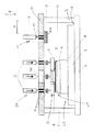
図1は、一実施形態における本発明で請求する作業空間13を有する装置を示しており、この作業空間13は、側壁7、カバー17およびベースプレート6によって境界が画定されている。
FIG. 1 shows an apparatus having a working
ベースプレート6の上には較正プレート5があり、この較正プレートは、ほぼ作業空間13の底部18全体にわたって延在している。
Above the
較正ベースプレート5の上には、較正テーブル4があり、この較正テーブルは、較正テーブル4の上に特に固定されて位置する基板ホルダ3を、作業空間13内で特にエンボス加工手段20および付与手段21に向けて動かすために、特にX方向にガイドされて動くことが可能である。基板ホルダ3は、受入手段24の構成要素である。
Above the
較正ベースプレート5および較正テーブル4は、較正手段22の構成要素であり、この較正手段は、上述した一連の移動を担う。さらに、較正手段22、特に較正テーブル4は、上に基板2が配置されている基板ホルダ3を、特に図1に示すX方向と図1から図面の紙面内を指すY方向とX方向およびY方向にわたる面Eにおける回転方向とにおいて、付与手段21に対して正確に較正し位置合せするように設計されている。ここで、位置決めおよび較正プロセスは、図示しない制御手段によって制御され、正確な位置合せは、基板2および/または基板ホルダ3の上の図示しないゲージマークを使用して行うことができる。
The
付与手段21のノズル本体12のノズル12dのZ方向における位置決めおよび較正は、付与アクチュエータ11によって行っており、カバー17を貫通するノズル本体のアクチュエータロッド19は、この付与アクチュエータ11に横断方向に、したがって面Eに対して平行に取り付けられている。
Positioning and calibration in the Z direction of the
構造材料1は、ノズル12dによって、基板2のノズル本体12と対向する上部2oに付与される。付与は、ステップアンドリピートプロセスで行う、すなわち、上部2oには、構造材料1がいくつかのステップで供給される。その際、構造材料1の規定された構造材料単位1e(図2参照)は、基板2の上部2oに付与され、そして後のエンボス加工プロセスにおいてエンボスダイ8の空隙8kに対応するように配置され、したがって、隆起構造15eとして後に硬化される構造領域のみに付与する。これに関して、付与手段21の個々の付与ステップがエンボス加工手段20の個々のエンボス加工ステップに対応する場合、有利である。したがって、ノズル12dは、特に、エンボスダイ8のエンボス加工面に対応する基板2の所定領域、または複数のこの領域を正確に覆う。
The
基板2の上部2oに構造材料1または構造材料単位1eが完全に供給されるとすぐに、基板2は、エンボス加工手段20に対向して配置され、図2および図3に示すエンボス加工プロセスを行うためにエンボスダイ8に対して較正される。
As soon as the
これもまた同様にステップアンドリピートプロセスで行い、エンボスダイ8を保持するダイ保持装置23とエンボスダイ23に作用するアクチュエータ10とによって、エンボスダイ8のエンボス加工力を構造材料1および基板2に加える。
This is similarly performed by a step-and-repeat process, and the embossing force of the embossing die 8 is applied to the
制御手段に接続された動力計セル9が、アクチュエータ10によって加えられる力および/または位置を測定する。また、3つのアクチュエータ10すべてを、位置制御してかつ/または力を制御して個々に使用してもよく、それにより、エンボス加工力を接触面の中心にシフトさせることにより、エッジ領域もまた均一にエンボス加工してもよい。
A dynamometer cell 9 connected to the control means measures the force and / or position applied by the
図3に示すエンボスダイ8の基板2に対する位置において、硬化プロセスを、特に、フォトレジストである構造材料1のUV露光により、カバー17の入口である窓14を通して行う。
In the position of the embossing die 8 with respect to the
アクチュエータ10によりエンボスダイ8を取り除いた後、図4に示す硬化した構造材料15が基板2上に残っており、この硬化した構造材料は、隆起構造15eと中間層厚さ16の中間層15zとからなる。残っている中間層厚さ16は、基板2を構造化するために、基板2全体を完全にエンボス加工し硬化させた後に、エッチングプロセスによって除去される。隆起構造15eは、エッチングマスクとして使用される。
After the embossing die 8 is removed by the
基板2について、構造化される基板は、円形基板または矩形基板、たとえば半導体ウェハ、ガラスウェハ、セラミック基板またはポリマー基板であってもよい。
For the
基板ホルダ3を、たとえば粘着保持装置または静電保持装置としてもよい。
The
エンボスダイ8を、たとえばホットエンボス加工、UVエンボス加工またはマイクロコンタクトプリンティングによって構造を打抜き加工またはエンボス加工するための、矩形ダイまたは円形ダイとしてもよい。 The embossing die 8 may be a rectangular die or a circular die for stamping or embossing the structure, for example by hot embossing, UV embossing or microcontact printing.
しかしながら、エンボスダイ8はまた、少なくとも部分的に石英、ガラスおよび/または混成構造からなってもよく、エンボスダイ8を、キャリア、補償層および構造層またはキャリアおよび弾性構造層から形成してもよい。 However, the embossing die 8 may also consist at least in part of quartz, glass and / or a hybrid structure, and the embossing die 8 may be formed of a carrier, a compensation layer and a structural layer or a carrier and an elastic structural layer. .
構造材料1は、たとえばUV光またはIR光によるレジストに対し、構造材料に応じて硬化する。
The
ノズル12dは、液滴として付与される構造材料単位1eの体積が、エンボスダイ8の空隙8kの体積に一致するように正確な大きさとなるように構成されており、液滴濃度および液滴体積は、可能な限り小さい中間層厚さ16が残るように、充填されるべき空隙8kの体積に従って大きさが決められる。液滴体積を、一定であるように有利に設定することができ、より大きい空隙8kに対して空隙8kごとに数滴を付与する。基板材料単位1eの一定の液滴体積は、最小空隙8kに対応してもよく、より大きい空隙8kに対して複数の基板材料単位1eを付与する。
The
硬化した構造材料15は、機能層として直接作用することができるが、上述したように、基板への構造転写用のエッチングマスクとして作用することも可能である。
The cured
1 構造材料、1e 構造材料単位、2 基板、2o 上部、3 基板ホルダ、4 較正テーブル(X、Y方向および回転)、5 較正ベースプレート、6 ベースプレート、7 側壁、8 エンボスダイ、8k 空隙、9 動力計セル、10 アクチュエータ、11 付与アクチュエータ、12 ノズル本体、12d ノズル、13 作業空間、14 窓、15 硬化した構造材料、15e 隆起構造、15z 中間層、16 中間層厚さ、17 カバー、18 底部、19 アクチュエータロッド、20 エンボス加工手段、21 付与手段、22 較正手段、23 ダイ保持装置、24 受入手段 1 structural material, 1e structural material unit, 2 substrate, 2o top, 3 substrate holder, 4 calibration table (X, Y direction and rotation), 5 calibration base plate, 6 base plate, 7 side wall, 8 embossing die, 8k air gap, 9 power Total cell, 10 Actuator, 11 Dispensing actuator, 12 Nozzle body, 12d nozzle, 13 Working space, 14 Window, 15 Hardened structural material, 15e Raised structure, 15z Intermediate layer, 16 Intermediate layer thickness, 17 Cover, 18 Bottom, 19 Actuator rod, 20 Embossing means, 21 Applying means, 22 Calibration means, 23 Die holding device, 24 Receiving means
Claims (14)
包囲された作業空間(13)を画定する側壁(7)、カバー(17)およびベースプレート(6)と、
前記包囲された作業空間(13)内に前記基板(2)を保持する少なくとも1つの受入手段(24)と、
前記包囲された作業空間(13)に少なくとも部分的に配置され、前記基板(2)を較正するための較正手段(22)と、
前記包囲された作業空間(13)に少なくとも部分的に配置され、エンボス加工プロセス中に前記基板(2)上に構造材料(1)をエンボス加工するためのエンボス加工手段(20)と、
前記包囲された作業空間(13)に少なくとも部分的に配置され、付与プロセス中に前記基板(2)に前記構造材料(1)を付与するための付与手段(21)であって、前記包囲された作業空間(13)に配置された少なくとも1つのノズル(12d)と、前記少なくとも1つのノズル(12d)を前記基板(2)の垂直方向に移動させるための付与アクチュエータ(11)と、を含む付与手段(21)と、
前記包囲された作業空間(13)を真空手段に選択的に接続するための真空ラインと、
を具備し、
前記構造材料(1)を前記基板(2)に付与する間、前記包囲された作業空間(13)の外側の気体圧力より低い気体圧力に前記基板(2)を晒すために、前記包囲された作業空間(13)は、前記付与プロセス中に前記真空手段に接続され、
前記包囲された作業空間(13)は、前記エンボス加工プロセスの前およびその間に、中断なく規定された雰囲気に晒される、
装置。 A device for embossing a substrate (2 ) ,
A side wall (7), a cover (17) and a base plate (6) defining an enclosed work space (13);
At least one receiving means for holding a pre-Symbol substrate (2) in the enclosed working space (13) and (24),
At least partially disposed in front Symbol enclosed working space (13), a front SL calibration means for calibrating the substrate (2) (22),
At least partially disposed in front Symbol enclosed working space (13), embossing means for the structural material (1) on the front Stories substrate (2) during e Nbosu machining process embossing (20) ,
An application means (21) disposed at least partially in the enclosed work space (13) and for applying the structural material (1) to the substrate (2) during an application process, the enclosure being enclosed And at least one nozzle (12d) arranged in the working space (13), and an application actuator (11) for moving the at least one nozzle (12d) in the vertical direction of the substrate (2). Providing means (21);
A vacuum line for selectively connecting the enclosed work space (13) to vacuum means;
Comprising
During the application of the structural material (1) to the substrate (2), the enclosed (2) is exposed to a gas pressure lower than the gas pressure outside the enclosed work space (13). A working space (13) is connected to the vacuum means during the application process,
The enclosed working space (13), before and during the e Nbosu machining process, Ru exposed to interruption without defined atmosphere,
Equipment.
請求項1に記載の装置。 Said defined atmosphere, before SL has low have gas pressure than the outer gas pressure of the surrounding working space (13), said defined atmosphere, there is no air body,
The apparatus according to 請 Motomeko 1.
請求項1または2に記載の装置。 The enclosed working space (13) through the vacuum line, exposed to pressure or pressure profile,
The apparatus according to claim 1 or 2.
請求項1から3のいずれか一項に記載の装置。 Produced as a step and repeat device that embosses the substrate (2) in several embossing steps in the embossing process.
Apparatus according to any one of claims 1 to 3.
前記エンボス構造は、ナノ構造またはナノ構造より小さい構造として作製される、
請求項1から4のいずれか一項に記載の装置。 The embossing means (20) has an embossing die (8) having an embossed structure which is embossed on the substrate (2),
The embossed structure is made as a nanostructure or a structure smaller than the nanostructure,
Apparatus according to any one of claims 1 to 4.
請求項1から5のいずれか一項に記載の装置。 The application means is configured to perform several application steps for applying the structural material (1) to a surface section of the substrate (2) during the application process .
Apparatus according to any one of claims 1 to 5 .
請求項1から6のいずれか一項に記載の装置。 The at least one nozzle (12d) is for applying the structural material (1) in droplet form ;
The device according to claim 1 .
請求項1から7のいずれか一項に記載の装置。 The application means (21) includes means for applying the structural material (1) by a spin method, a screen printing method, a spray method, or a piezo method.
Apparatus according to any one of claims 1 to 7.
請求項1から8のいずれか一項に記載の装置。 Before Symbol structural material (1), as will be granted only to structural region corresponding to the gap (8k) of the embossing die in a defined structural material units (1e) (8), for controlling the applying process The method further includes:
Apparatus according to any one of claims 1 to 8 .
請求項9に記載の装置。 The structural material units (1e) has the corresponding air gap (8k) good Redirecting a listening volume of the embossing die (8),
The apparatus according to claim 9 .
前記方法は、
a)前記基板(2)を、包囲された作業空間(13)に少なくとも部分的に配置された較正手段(22)によって、付与手段(21)に対して較正するステップと、
b)前記包囲された作業空間(13)に配置された少なくとも1つのノズル(12d)と、前記少なくとも1つのノズル(12d)を前記基板(2)の垂直方向に移動させるための付与アクチュエータ(11)と、を含む前記付与手段(21)によって、付与プロセス中に、構造材料(1)を前記基板(2)に付与するステップと、
c)前記包囲された作業空間(13)を真空手段に選択的に接続するための真空ラインによって、前記構造材料(1)を前記基板(2)に付与する間、前記包囲された作業空間(13)の外側の気体圧力より低い気体圧力に前記基板(2)を晒すために、前記付与プロセス中に、前記包囲された作業空間(13)を前記真空手段に接続するステップと、
d)前記基板(2)を、前記較正手段(22)によって、前記包囲された作業空間(13)に少なくとも部分的に配置され、エンボス加工プロセス中に前記基板(2)上に前記構造材料(1)をエンボス加工するためのエンボス加工手段(20)に対して較正するステップと、
e)前記基板(2)に前記エンボス加工手段(20)によってエンボス加工するステップであって、前記エンボス加工プロセスの前およびその間に前記包囲された作業空間(13)に、中断なく規定された雰囲気が供給される、ステップと、
を含む方法。 A method for embossing a substrate (2 ) ,
The method
The a) the substrate (2), by at least partially disposed calibration means enclosed working space (13) (22), comprising the steps of calibrated against the grant means (21),
b) At least one nozzle (12d) arranged in the enclosed work space (13) and an application actuator (11) for moving the at least one nozzle (12d) in the vertical direction of the substrate (2) And applying the structural material (1) to the substrate (2) during the application process by the application means (21) comprising:
c) While the structural material (1) is applied to the substrate (2) by a vacuum line for selectively connecting the enclosed work space (13) to vacuum means, the enclosed work space ( Connecting the enclosed work space (13) to the vacuum means during the application process to expose the substrate (2) to a gas pressure lower than the gas pressure outside of 13);
The d) said substrate (2), by the calibration means (22) is at least partially disposed in the enclosed work space (13), said structural material said on the substrate (2) during the embossing process ( and steps for calibrating against a 1) embossing means for embossing (20),
comprising the steps of embossing by e) said embossing means the substrate (2) (20), the working space before and surrounded pre SL during the embossing process (13) is defined interruption without The atmosphere is supplied, steps,
Including methods.
前記規定された雰囲気は、気体がない、
請求項11に記載の方法。 Said defined atmosphere having a low have gas pressure than the outer gas pressure before Symbol enclosed working space (13),
Said defined atmosphere, there is no care body,
The method of claim 11 .
請求項11または12に記載の方法。 Step b) is a defined atmosphere, empty pneumatic methods, thermal methods, piezo printing, scan screen printing, SPRAY method, or carried out by spin method,
The method according to claim 11 or 12 .
請求項11から13のいずれか一項に記載の方法。 The grant process according to step b) is a d Nbosudai (8) corresponds to the gap (8k) good Redirecting a is not the body volume can defined structure material units (1e), the gap of the embossing die (8) Controlled so that the structural material (1) is applied only to the structural region corresponding to (8k),
The method according to any one of claims 11 to 13 .
Applications Claiming Priority (2)
| Application Number | Priority Date | Filing Date | Title |
|---|---|---|---|
| EP09010779.8 | 2009-08-22 | ||
| EP20090010779 EP2287666B1 (en) | 2009-08-22 | 2009-08-22 | Device for embossing substrates |
Publications (3)
| Publication Number | Publication Date |
|---|---|
| JP2011044715A JP2011044715A (en) | 2011-03-03 |
| JP2011044715A5 JP2011044715A5 (en) | 2013-06-13 |
| JP5693090B2 true JP5693090B2 (en) | 2015-04-01 |
Family
ID=41429335
Family Applications (1)
| Application Number | Title | Priority Date | Filing Date |
|---|---|---|---|
| JP2010185136A Active JP5693090B2 (en) | 2009-08-22 | 2010-08-20 | Equipment for embossing substrates |
Country Status (3)
| Country | Link |
|---|---|
| US (2) | US9116424B2 (en) |
| EP (1) | EP2287666B1 (en) |
| JP (1) | JP5693090B2 (en) |
Families Citing this family (5)
| Publication number | Priority date | Publication date | Assignee | Title |
|---|---|---|---|---|
| JP4814682B2 (en) * | 2006-04-18 | 2011-11-16 | 株式会社日立ハイテクノロジーズ | Fine structure pattern transfer method and transfer apparatus |
| CN103558801A (en) * | 2013-11-08 | 2014-02-05 | 无锡英普林纳米科技有限公司 | Nanometer imprinting equipment |
| WO2015161868A1 (en) * | 2014-04-22 | 2015-10-29 | Ev Group E. Thallner Gmbh | Method and device for embossing a nanostructure |
| JP6489309B2 (en) * | 2015-05-14 | 2019-03-27 | パナソニックIpマネジメント株式会社 | Imprint method and imprint apparatus |
| WO2022008033A1 (en) | 2020-07-06 | 2022-01-13 | Ev Group E. Thallner Gmbh | Apparatus and method for producing micro- and/or nano-structures |
Family Cites Families (16)
| Publication number | Priority date | Publication date | Assignee | Title |
|---|---|---|---|---|
| EP0741001B1 (en) * | 1995-05-04 | 2002-02-06 | Gietz AG | Stamping, printing and punching machine |
| US20050160934A1 (en) * | 2004-01-23 | 2005-07-28 | Molecular Imprints, Inc. | Materials and methods for imprint lithography |
| FI20030919A (en) * | 2003-06-19 | 2004-12-20 | Avantone Oy | Method and apparatus for manufacturing an electronic thin film component and the electronic thin film component |
| JP2005101201A (en) * | 2003-09-24 | 2005-04-14 | Canon Inc | Nano-imprint system |
| JP4069081B2 (en) * | 2004-01-13 | 2008-03-26 | 東京エレクトロン株式会社 | Position adjustment method and substrate processing system |
| JP4481698B2 (en) | 2004-03-29 | 2010-06-16 | キヤノン株式会社 | Processing equipment |
| JP4574240B2 (en) * | 2004-06-11 | 2010-11-04 | キヤノン株式会社 | Processing apparatus, processing method, device manufacturing method |
| US8011916B2 (en) | 2005-09-06 | 2011-09-06 | Canon Kabushiki Kaisha | Mold, imprint apparatus, and process for producing structure |
| US7670534B2 (en) * | 2005-09-21 | 2010-03-02 | Molecular Imprints, Inc. | Method to control an atmosphere between a body and a substrate |
| US7491049B2 (en) * | 2005-09-30 | 2009-02-17 | Hon Hai Precision Industry Co., Ltd. | Apparatus for hot embossing lithography |
| EP1958025B1 (en) * | 2005-12-08 | 2011-05-18 | Molecular Imprints, Inc. | Method for expelling gas positioned between a substrate and a mold |
| JPWO2007094213A1 (en) | 2006-02-14 | 2009-07-02 | パイオニア株式会社 | Imprint apparatus and imprint method |
| JP4536148B2 (en) * | 2006-04-03 | 2010-09-01 | モレキュラー・インプリンツ・インコーポレーテッド | Lithography imprint system |
| JP4995478B2 (en) * | 2006-04-18 | 2012-08-08 | 株式会社日立ハイテクノロジーズ | Nanoimprint spacer, method for producing electron microscope adjustment sample using the same, electron microscope adjustment sample, and electron microscope equipped with the same |
| JP4908369B2 (en) | 2007-10-02 | 2012-04-04 | 株式会社東芝 | Imprint method and imprint system |
| NL1036034A1 (en) * | 2007-10-11 | 2009-04-15 | Asml Netherlands Bv | Imprint lithography. |
-
2009
- 2009-08-22 EP EP20090010779 patent/EP2287666B1/en active Active
-
2010
- 2010-08-18 US US12/858,509 patent/US9116424B2/en active Active
- 2010-08-20 JP JP2010185136A patent/JP5693090B2/en active Active
-
2015
- 2015-05-20 US US14/717,003 patent/US10239253B2/en active Active
Also Published As
| Publication number | Publication date |
|---|---|
| US10239253B2 (en) | 2019-03-26 |
| US20110045185A1 (en) | 2011-02-24 |
| EP2287666A1 (en) | 2011-02-23 |
| US9116424B2 (en) | 2015-08-25 |
| EP2287666B1 (en) | 2012-06-27 |
| US20150251349A1 (en) | 2015-09-10 |
| JP2011044715A (en) | 2011-03-03 |
Similar Documents
| Publication | Publication Date | Title |
|---|---|---|
| CN102929099B (en) | Imprinting apparatus and article manufacturing method | |
| EP3766097A1 (en) | Planarization for semiconductor device package fabrication processes | |
| JP5693090B2 (en) | Equipment for embossing substrates | |
| JP2010076300A (en) | Processing apparatus | |
| CN108732862B (en) | Imprint apparatus and method of manufacturing article | |
| JP2009532899A (en) | Chuck system with an array of fluid chambers | |
| TW201838790A (en) | Imprint apparatus and method of manufacturing article | |
| JP2018092996A (en) | Imprint method, imprint device, mold, and method of manufacturing article | |
| KR20220100690A (en) | Wafer Processes, Apparatuses, and Methods of Making Articles | |
| JP2017112230A (en) | Imprint device and article manufacturing method | |
| JP5822597B2 (en) | Imprint apparatus and article manufacturing method using the same | |
| JP4625247B2 (en) | Micro contact printing method and apparatus | |
| KR20200136827A (en) | Lithography apparatus and method of manufacturing article | |
| JP6391709B2 (en) | Method and apparatus for embossing nanostructures | |
| TWI654060B (en) | Imprinting device, imprinting method and article manufacturing method | |
| JP2012099789A (en) | Imprint device and manufacturing method of article | |
| JP2022064288A (en) | Chuck assembly, planarization process, apparatus and method for manufacturing article | |
| KR101215990B1 (en) | Imprint apparatus and imprint method using it | |
| US20230112924A1 (en) | Substrate conveyance method, substrate conveyance apparatus, molding method, and article manufacturing method | |
| JP7254564B2 (en) | IMPRINT APPARATUS, IMPRINT METHOD, AND ARTICLE MANUFACTURING METHOD | |
| JP7267783B2 (en) | Flattening apparatus, flattening method and article manufacturing method | |
| US20230063974A1 (en) | Molding apparatus, molding method, and method for manufacturing a product | |
| JP2020107863A (en) | Film formation device and production method of article | |
| JP2020202270A (en) | Membrane forming device and article manufacturing method | |
| JP2018085479A (en) | Mold holding device, imprint apparatus, and method of manufacturing article |
Legal Events
| Date | Code | Title | Description |
|---|---|---|---|
| A521 | Request for written amendment filed |
Free format text: JAPANESE INTERMEDIATE CODE: A523 Effective date: 20130424 |
|
| A621 | Written request for application examination |
Free format text: JAPANESE INTERMEDIATE CODE: A621 Effective date: 20130424 |
|
| A977 | Report on retrieval |
Free format text: JAPANESE INTERMEDIATE CODE: A971007 Effective date: 20140227 |
|
| A131 | Notification of reasons for refusal |
Free format text: JAPANESE INTERMEDIATE CODE: A131 Effective date: 20140310 |
|
| RD03 | Notification of appointment of power of attorney |
Free format text: JAPANESE INTERMEDIATE CODE: A7423 Effective date: 20140320 |
|
| RD04 | Notification of resignation of power of attorney |
Free format text: JAPANESE INTERMEDIATE CODE: A7424 Effective date: 20140331 |
|
| A521 | Request for written amendment filed |
Free format text: JAPANESE INTERMEDIATE CODE: A523 Effective date: 20140529 |
|
| TRDD | Decision of grant or rejection written | ||
| A01 | Written decision to grant a patent or to grant a registration (utility model) |
Free format text: JAPANESE INTERMEDIATE CODE: A01 Effective date: 20150105 |
|
| A61 | First payment of annual fees (during grant procedure) |
Free format text: JAPANESE INTERMEDIATE CODE: A61 Effective date: 20150203 |
|
| R150 | Certificate of patent or registration of utility model |
Ref document number: 5693090 Country of ref document: JP Free format text: JAPANESE INTERMEDIATE CODE: R150 |
|
| R250 | Receipt of annual fees |
Free format text: JAPANESE INTERMEDIATE CODE: R250 |
|
| R250 | Receipt of annual fees |
Free format text: JAPANESE INTERMEDIATE CODE: R250 |
|
| R250 | Receipt of annual fees |
Free format text: JAPANESE INTERMEDIATE CODE: R250 |
|
| R250 | Receipt of annual fees |
Free format text: JAPANESE INTERMEDIATE CODE: R250 |
|
| R250 | Receipt of annual fees |
Free format text: JAPANESE INTERMEDIATE CODE: R250 |
|
| R250 | Receipt of annual fees |
Free format text: JAPANESE INTERMEDIATE CODE: R250 |
|
| R250 | Receipt of annual fees |
Free format text: JAPANESE INTERMEDIATE CODE: R250 |