JP5689245B2 - Nitride semiconductor device - Google Patents
Nitride semiconductor device Download PDFInfo
- Publication number
- JP5689245B2 JP5689245B2 JP2010089842A JP2010089842A JP5689245B2 JP 5689245 B2 JP5689245 B2 JP 5689245B2 JP 2010089842 A JP2010089842 A JP 2010089842A JP 2010089842 A JP2010089842 A JP 2010089842A JP 5689245 B2 JP5689245 B2 JP 5689245B2
- Authority
- JP
- Japan
- Prior art keywords
- layer
- nitride semiconductor
- semiconductor device
- spacer layer
- spacer
- Prior art date
- Legal status (The legal status is an assumption and is not a legal conclusion. Google has not performed a legal analysis and makes no representation as to the accuracy of the status listed.)
- Active
Links
- 239000004065 semiconductor Substances 0.000 title claims description 100
- 150000004767 nitrides Chemical class 0.000 title claims description 82
- 125000006850 spacer group Chemical group 0.000 claims description 89
- 239000000758 substrate Substances 0.000 claims description 64
- 230000001629 suppression Effects 0.000 claims description 26
- 239000000203 mixture Substances 0.000 claims description 17
- 229910052710 silicon Inorganic materials 0.000 claims description 10
- XUIMIQQOPSSXEZ-UHFFFAOYSA-N Silicon Chemical compound [Si] XUIMIQQOPSSXEZ-UHFFFAOYSA-N 0.000 claims description 9
- 239000010703 silicon Substances 0.000 claims description 9
- 229910002601 GaN Inorganic materials 0.000 description 23
- 230000015556 catabolic process Effects 0.000 description 17
- PMHQVHHXPFUNSP-UHFFFAOYSA-M copper(1+);methylsulfanylmethane;bromide Chemical compound Br[Cu].CSC PMHQVHHXPFUNSP-UHFFFAOYSA-M 0.000 description 12
- 229910002704 AlGaN Inorganic materials 0.000 description 10
- 230000004888 barrier function Effects 0.000 description 8
- 239000013078 crystal Substances 0.000 description 7
- 230000000694 effects Effects 0.000 description 7
- 238000000034 method Methods 0.000 description 6
- 229910052594 sapphire Inorganic materials 0.000 description 6
- 239000010980 sapphire Substances 0.000 description 6
- 230000007547 defect Effects 0.000 description 5
- JMASRVWKEDWRBT-UHFFFAOYSA-N Gallium nitride Chemical compound [Ga]#N JMASRVWKEDWRBT-UHFFFAOYSA-N 0.000 description 4
- 230000006835 compression Effects 0.000 description 4
- 238000007906 compression Methods 0.000 description 4
- 229910052751 metal Inorganic materials 0.000 description 4
- 239000002184 metal Substances 0.000 description 4
- 238000004519 manufacturing process Methods 0.000 description 3
- 238000002488 metal-organic chemical vapour deposition Methods 0.000 description 3
- 239000002994 raw material Substances 0.000 description 3
- QGZKDVFQNNGYKY-UHFFFAOYSA-N Ammonia Chemical compound N QGZKDVFQNNGYKY-UHFFFAOYSA-N 0.000 description 2
- 238000007796 conventional method Methods 0.000 description 2
- 230000005669 field effect Effects 0.000 description 2
- 239000012535 impurity Substances 0.000 description 2
- 239000000463 material Substances 0.000 description 2
- 238000005259 measurement Methods 0.000 description 2
- PIGFYZPCRLYGLF-UHFFFAOYSA-N Aluminum nitride Chemical compound [Al]#N PIGFYZPCRLYGLF-UHFFFAOYSA-N 0.000 description 1
- UFHFLCQGNIYNRP-UHFFFAOYSA-N Hydrogen Chemical compound [H][H] UFHFLCQGNIYNRP-UHFFFAOYSA-N 0.000 description 1
- 230000002159 abnormal effect Effects 0.000 description 1
- 239000000956 alloy Substances 0.000 description 1
- 229910045601 alloy Inorganic materials 0.000 description 1
- RNQKDQAVIXDKAG-UHFFFAOYSA-N aluminum gallium Chemical compound [Al].[Ga] RNQKDQAVIXDKAG-UHFFFAOYSA-N 0.000 description 1
- 229910021529 ammonia Inorganic materials 0.000 description 1
- 230000015572 biosynthetic process Effects 0.000 description 1
- 239000012159 carrier gas Substances 0.000 description 1
- 238000005229 chemical vapour deposition Methods 0.000 description 1
- 230000007423 decrease Effects 0.000 description 1
- 230000005684 electric field Effects 0.000 description 1
- 238000001887 electron backscatter diffraction Methods 0.000 description 1
- 238000002003 electron diffraction Methods 0.000 description 1
- 229910052733 gallium Inorganic materials 0.000 description 1
- 230000017525 heat dissipation Effects 0.000 description 1
- 150000004678 hydrides Chemical class 0.000 description 1
- 239000001257 hydrogen Substances 0.000 description 1
- 229910052739 hydrogen Inorganic materials 0.000 description 1
- 229910052738 indium Inorganic materials 0.000 description 1
- APFVFJFRJDLVQX-UHFFFAOYSA-N indium atom Chemical compound [In] APFVFJFRJDLVQX-UHFFFAOYSA-N 0.000 description 1
- 238000000691 measurement method Methods 0.000 description 1
- 238000012986 modification Methods 0.000 description 1
- 230000004048 modification Effects 0.000 description 1
- JLTRXTDYQLMHGR-UHFFFAOYSA-N trimethylaluminium Chemical compound C[Al](C)C JLTRXTDYQLMHGR-UHFFFAOYSA-N 0.000 description 1
- XCZXGTMEAKBVPV-UHFFFAOYSA-N trimethylgallium Chemical compound C[Ga](C)C XCZXGTMEAKBVPV-UHFFFAOYSA-N 0.000 description 1
- 230000005533 two-dimensional electron gas Effects 0.000 description 1
- 238000001947 vapour-phase growth Methods 0.000 description 1
Images


Classifications
-
- H—ELECTRICITY
- H01—ELECTRIC ELEMENTS
- H01L—SEMICONDUCTOR DEVICES NOT COVERED BY CLASS H10
- H01L21/00—Processes or apparatus adapted for the manufacture or treatment of semiconductor or solid state devices or of parts thereof
- H01L21/02—Manufacture or treatment of semiconductor devices or of parts thereof
- H01L21/02104—Forming layers
- H01L21/02365—Forming inorganic semiconducting materials on a substrate
- H01L21/02367—Substrates
- H01L21/0237—Materials
- H01L21/02373—Group 14 semiconducting materials
- H01L21/02381—Silicon, silicon germanium, germanium
-
- H—ELECTRICITY
- H01—ELECTRIC ELEMENTS
- H01L—SEMICONDUCTOR DEVICES NOT COVERED BY CLASS H10
- H01L21/00—Processes or apparatus adapted for the manufacture or treatment of semiconductor or solid state devices or of parts thereof
- H01L21/02—Manufacture or treatment of semiconductor devices or of parts thereof
- H01L21/02104—Forming layers
- H01L21/02365—Forming inorganic semiconducting materials on a substrate
- H01L21/02436—Intermediate layers between substrates and deposited layers
- H01L21/02439—Materials
- H01L21/02455—Group 13/15 materials
- H01L21/02458—Nitrides
-
- H—ELECTRICITY
- H01—ELECTRIC ELEMENTS
- H01L—SEMICONDUCTOR DEVICES NOT COVERED BY CLASS H10
- H01L21/00—Processes or apparatus adapted for the manufacture or treatment of semiconductor or solid state devices or of parts thereof
- H01L21/02—Manufacture or treatment of semiconductor devices or of parts thereof
- H01L21/02104—Forming layers
- H01L21/02365—Forming inorganic semiconducting materials on a substrate
- H01L21/02436—Intermediate layers between substrates and deposited layers
- H01L21/02494—Structure
- H01L21/02496—Layer structure
- H01L21/02505—Layer structure consisting of more than two layers
- H01L21/02507—Alternating layers, e.g. superlattice
-
- H—ELECTRICITY
- H01—ELECTRIC ELEMENTS
- H01L—SEMICONDUCTOR DEVICES NOT COVERED BY CLASS H10
- H01L21/00—Processes or apparatus adapted for the manufacture or treatment of semiconductor or solid state devices or of parts thereof
- H01L21/02—Manufacture or treatment of semiconductor devices or of parts thereof
- H01L21/02104—Forming layers
- H01L21/02365—Forming inorganic semiconducting materials on a substrate
- H01L21/02518—Deposited layers
- H01L21/02521—Materials
- H01L21/02538—Group 13/15 materials
- H01L21/0254—Nitrides
-
- H—ELECTRICITY
- H01—ELECTRIC ELEMENTS
- H01L—SEMICONDUCTOR DEVICES NOT COVERED BY CLASS H10
- H01L29/00—Semiconductor devices specially adapted for rectifying, amplifying, oscillating or switching and having potential barriers; Capacitors or resistors having potential barriers, e.g. a PN-junction depletion layer or carrier concentration layer; Details of semiconductor bodies or of electrodes thereof ; Multistep manufacturing processes therefor
- H01L29/66—Types of semiconductor device ; Multistep manufacturing processes therefor
- H01L29/68—Types of semiconductor device ; Multistep manufacturing processes therefor controllable by only the electric current supplied, or only the electric potential applied, to an electrode which does not carry the current to be rectified, amplified or switched
- H01L29/76—Unipolar devices, e.g. field effect transistors
- H01L29/772—Field effect transistors
- H01L29/778—Field effect transistors with two-dimensional charge carrier gas channel, e.g. HEMT ; with two-dimensional charge-carrier layer formed at a heterojunction interface
- H01L29/7786—Field effect transistors with two-dimensional charge carrier gas channel, e.g. HEMT ; with two-dimensional charge-carrier layer formed at a heterojunction interface with direct single heterostructure, i.e. with wide bandgap layer formed on top of active layer, e.g. direct single heterostructure MIS-like HEMT
- H01L29/7787—Field effect transistors with two-dimensional charge carrier gas channel, e.g. HEMT ; with two-dimensional charge-carrier layer formed at a heterojunction interface with direct single heterostructure, i.e. with wide bandgap layer formed on top of active layer, e.g. direct single heterostructure MIS-like HEMT with wide bandgap charge-carrier supplying layer, e.g. direct single heterostructure MODFET
-
- H—ELECTRICITY
- H01—ELECTRIC ELEMENTS
- H01L—SEMICONDUCTOR DEVICES NOT COVERED BY CLASS H10
- H01L29/00—Semiconductor devices specially adapted for rectifying, amplifying, oscillating or switching and having potential barriers; Capacitors or resistors having potential barriers, e.g. a PN-junction depletion layer or carrier concentration layer; Details of semiconductor bodies or of electrodes thereof ; Multistep manufacturing processes therefor
- H01L29/66—Types of semiconductor device ; Multistep manufacturing processes therefor
- H01L29/86—Types of semiconductor device ; Multistep manufacturing processes therefor controllable only by variation of the electric current supplied, or only the electric potential applied, to one or more of the electrodes carrying the current to be rectified, amplified, oscillated or switched
- H01L29/861—Diodes
- H01L29/872—Schottky diodes
-
- H—ELECTRICITY
- H01—ELECTRIC ELEMENTS
- H01L—SEMICONDUCTOR DEVICES NOT COVERED BY CLASS H10
- H01L29/00—Semiconductor devices specially adapted for rectifying, amplifying, oscillating or switching and having potential barriers; Capacitors or resistors having potential barriers, e.g. a PN-junction depletion layer or carrier concentration layer; Details of semiconductor bodies or of electrodes thereof ; Multistep manufacturing processes therefor
- H01L29/02—Semiconductor bodies ; Multistep manufacturing processes therefor
- H01L29/12—Semiconductor bodies ; Multistep manufacturing processes therefor characterised by the materials of which they are formed
- H01L29/20—Semiconductor bodies ; Multistep manufacturing processes therefor characterised by the materials of which they are formed including, apart from doping materials or other impurities, only AIIIBV compounds
- H01L29/2003—Nitride compounds
Landscapes
- Engineering & Computer Science (AREA)
- Microelectronics & Electronic Packaging (AREA)
- Power Engineering (AREA)
- Physics & Mathematics (AREA)
- Condensed Matter Physics & Semiconductors (AREA)
- General Physics & Mathematics (AREA)
- Computer Hardware Design (AREA)
- Manufacturing & Machinery (AREA)
- Ceramic Engineering (AREA)
- Chemical & Material Sciences (AREA)
- Materials Engineering (AREA)
- Junction Field-Effect Transistors (AREA)
Description
本発明は窒化物半導体素子に関し、特にシリコン基板上に形成された窒化物半導体素子に関する。 The present invention relates to a nitride semiconductor device, and more particularly to a nitride semiconductor device formed on a silicon substrate.
窒化物半導体である窒化ガリウム(以下GaN)は、電子飽和速度が大きく、絶縁破壊電界が高い。また、高い熱伝導率を有することにより放熱性に優れ、高温での動作が可能であるという特性を有している。さらに、窒化アルミニウムガリウム(以下AlGaN)とGaNとのヘテロ界面にピエゾ効果による高濃度の2次元電子ガス(以下2DEG)が発生する。2DEGをチャネルとして用いることにより、大電流動作が可能となり、低損失で高効率のヘテロ構造電界効果トランジスタ(以下HFET)に代表されるパワーデバイスの実現が期待されている。 Gallium nitride (hereinafter GaN), which is a nitride semiconductor, has a high electron saturation rate and a high breakdown electric field. Moreover, it has the characteristics that it has excellent heat dissipation due to its high thermal conductivity and can operate at high temperatures. Furthermore, a high-concentration two-dimensional electron gas (hereinafter referred to as 2DEG) is generated at the heterointerface between aluminum gallium nitride (hereinafter referred to as AlGaN) and GaN due to the piezoelectric effect. By using 2DEG as a channel, a large current operation is possible, and realization of a power device represented by a low-loss and high-efficiency heterostructure field effect transistor (hereinafter referred to as HFET) is expected.
窒化物半導体層を成長させる基板にGaN基板を用いれば格子定数が一致しているため、結晶構造が良好な窒化物半導体層を容易に形成することができる。しかし、GaN基板は高価である。このため、安価なサファイア基板又はシリコン(Si)基板等の上に窒化物半導体層を形成することが検討されている。しかし、サファイア及びSiは、結晶の格子定数が窒化物半導体とは大きく異なっている。従って、これらの基板の上に成長させた窒化物半導体層には、格子欠陥が発生しやすい。格子欠陥はリーク電流や、いわゆる電流コラプスの原因となる。このため、サファイア基板の上にアンドープのGaN層と、窒化インジウムガリウム(InGaN)及びAlGaNを積層した超格子層とを設け、その上に形成する窒化物半導体層の格子欠陥を低減することが試みられている(例えば、特許文献1を参照。)。 If a GaN substrate is used as the substrate on which the nitride semiconductor layer is grown, the lattice constants coincide with each other, so that a nitride semiconductor layer having a good crystal structure can be easily formed. However, GaN substrates are expensive. For this reason, formation of a nitride semiconductor layer on an inexpensive sapphire substrate or silicon (Si) substrate has been studied. However, sapphire and Si are significantly different in crystal lattice constant from nitride semiconductors. Accordingly, lattice defects are likely to occur in the nitride semiconductor layer grown on these substrates. Lattice defects cause leakage current and so-called current collapse. For this reason, an undoped GaN layer and a superlattice layer in which indium gallium nitride (InGaN) and AlGaN are stacked are provided on a sapphire substrate, and attempts are made to reduce lattice defects in the nitride semiconductor layer formed thereon. (For example, see Patent Document 1).
サファイア基板は、GaN基板と比べると安価であるが、Si基板と比べると価格が高く基板の径も小さい。このため、パワーデバイスのコストをさらに低減するために、安価で且つ大口径の基板を容易に入手できるSi基板を用いて窒化物半導体素子を形成することが検討されている。Si基板の場合、窒化物半導体層との格子定数の差は、サファイア基板よりも大きくなる。また、Si基板と窒化物半導体層との熱膨張係数の差も非常に大きいため、Si基板上に成長した窒化物半導体層にはクラックと呼ばれる微細な割れが生じやすい。クラックを低減するために、Si基板と動作層との間にGaN層と窒化アルミニウム(以下AlN)層とを積層した超格子層を形成することが検討されている(例えば、非特許文献1を参照。)。 A sapphire substrate is less expensive than a GaN substrate, but is more expensive and smaller in diameter than a Si substrate. For this reason, in order to further reduce the cost of the power device, it has been studied to form a nitride semiconductor element using a Si substrate that is inexpensive and can easily obtain a large-diameter substrate. In the case of a Si substrate, the difference in lattice constant from the nitride semiconductor layer is larger than that of a sapphire substrate. In addition, since the difference in thermal expansion coefficient between the Si substrate and the nitride semiconductor layer is also very large, fine cracks called cracks are likely to occur in the nitride semiconductor layer grown on the Si substrate. In order to reduce cracks, it has been studied to form a superlattice layer in which a GaN layer and an aluminum nitride (hereinafter referred to as AlN) layer are stacked between an Si substrate and an operation layer (for example, see Non-Patent Document 1). reference.).
しかしながら、従来のGaNとAlNとを積層した超格子層を用いてSi基板の上に窒化物半導体素子を形成する場合には、以下のような問題が生じることが明らかとなった。コスト低減のためには大口径のSi基板を用いて窒化物半導体素子を形成することが好ましい。また、不良の発生をできるだけ抑える必要がある。しかし、大口径のSi基板の上に窒化物半導体層を形成すると、反りが非常に大きくなる。このため、従来の方法では、反りによるクラック及び基板の割れの発生を抑えることが困難となる。従って、大口径のSi基板を用いても歩留まりが低く、生産性を向上させることができない。特に、パワーデバイスの場合には、耐圧を確保するために基板上に比較的厚い半導体層を形成する必要がある。このため、反りがさらに大きくなる傾向にある。従来の方法では、径が75mm(3インチ)以上のSi基板を用いることは実用上不可能であることが明らかとなった。 However, it has been clarified that the following problems arise when a nitride semiconductor element is formed on a Si substrate using a conventional superlattice layer in which GaN and AlN are laminated. In order to reduce costs, it is preferable to form a nitride semiconductor element using a large-diameter Si substrate. Moreover, it is necessary to suppress the occurrence of defects as much as possible. However, when a nitride semiconductor layer is formed on a large-diameter Si substrate, warping becomes very large. For this reason, with the conventional method, it is difficult to suppress the occurrence of cracks due to warpage and substrate cracks. Therefore, even if a large-diameter Si substrate is used, the yield is low and productivity cannot be improved. In particular, in the case of a power device, it is necessary to form a relatively thick semiconductor layer on the substrate in order to ensure a breakdown voltage. For this reason, there exists a tendency for curvature to become still larger. In the conventional method, it has become clear that it is practically impossible to use a Si substrate having a diameter of 75 mm (3 inches) or more.
また、Si基板においてサファイア基板のようにGaN層と、InGaN及びAlGaNを積層した超格子層とを設けることにより格子欠陥の発生を抑えようとすると、反りがさらに大きくなることも明らかとなった。 In addition, it has also been clarified that warpage is further increased when an attempt is made to suppress the generation of lattice defects by providing a GaN layer and a superlattice layer in which InGaN and AlGaN are stacked on a Si substrate as in a sapphire substrate.
本発明は、前記の問題を解決し、Si基板の上に形成した窒化物半導体素子の生産性及び動作特性を向上させることを目的とする。 An object of the present invention is to solve the above problems and improve the productivity and operating characteristics of a nitride semiconductor device formed on a Si substrate.
前記の目的を達成するため、本発明は窒化物半導体素子を、第1の窒化物半導体層と、第1の窒化物半導体層よりも格子定数が小さい第2の窒化物半導体層と、平均の格子定数が第1の窒化物半導体層よりも小さく且つ第2の窒化物半導体層よりも大きい超格子層とを含む歪み抑制層を有する構成とする。 In order to achieve the above object, the present invention provides a nitride semiconductor device comprising: a first nitride semiconductor layer; a second nitride semiconductor layer having a lattice constant smaller than that of the first nitride semiconductor layer; The strain suppression layer includes a superlattice layer having a lattice constant smaller than that of the first nitride semiconductor layer and larger than that of the second nitride semiconductor layer.
具体的に、本発明に係る窒化物半導体素子は、シリコン基板と、シリコン基板の上に初期層を介して形成された歪み抑制層と、歪み抑制層の上に形成された動作層とを備えている。歪み抑制層は、第1の窒化物半導体からなる第1のスペーサ層と、第1のスペーサ層の上に接して形成され、第1の窒化物半導体よりも格子定数が小さい第2の窒化物半導体からなる第2のスペーサ層と、第2のスペーサ層の上に接して形成され、第3の窒化物半導体からなる第1の層及び第3の窒化物半導体よりも格子定数が小さい第4の窒化物半導体からなる第2の層が交互に積層された超格子層とを有している。超格子層は、平均の格子定数が第1のスペーサ層の格子定数よりも小さく且つ第2のスペーサ層の格子定数よりも大きい。 Specifically, a nitride semiconductor device according to the present invention includes a silicon substrate, a strain suppression layer formed on the silicon substrate via an initial layer, and an operation layer formed on the strain suppression layer. ing. The strain suppression layer is formed on and in contact with the first spacer layer made of the first nitride semiconductor, and the second nitride having a lattice constant smaller than that of the first nitride semiconductor. A second spacer layer made of a semiconductor and a fourth layer formed on and in contact with the second spacer layer and having a lattice constant smaller than that of the first layer made of the third nitride semiconductor and the third nitride semiconductor; And a superlattice layer in which second layers made of the nitride semiconductor are alternately stacked. The superlattice layer has an average lattice constant smaller than that of the first spacer layer and larger than that of the second spacer layer.
本発明の窒化物半導体素子は、歪み抑制層が、格子定数が大きい第1のスペーサ層と、その上に接して形成された格子定数が小さい第2のスペーサ層と、その上に接して形成された中間の格子定数を有する超格子層とを含む。このため、圧縮歪みと伸張歪みとのバランスを取ることができる。これにより、Si基板及びその上に形成された窒化物半導体層の反りを小さくすることが可能となる。また、歪み抑制層が超格子層を含むので、動作層とシリコン基板との間隔を広くして耐圧を確保することができると共に、クラックの発生をさらに低減することができる。 In the nitride semiconductor device of the present invention, the strain suppression layer is formed in contact with the first spacer layer having a large lattice constant, the second spacer layer having a small lattice constant formed thereon and in contact therewith. And a superlattice layer having an intermediate lattice constant. For this reason, it is possible to balance the compression strain and the extension strain. As a result, the warpage of the Si substrate and the nitride semiconductor layer formed thereon can be reduced. In addition, since the strain suppression layer includes a superlattice layer, it is possible to widen the distance between the operation layer and the silicon substrate to ensure a withstand voltage, and to further reduce the occurrence of cracks.
本発明の窒化物半導体素子において、第1の層は、格子定数が第1のスペーサ層よりも小さくてもよい。 In the nitride semiconductor device of the present invention, the first layer may have a lattice constant smaller than that of the first spacer layer.
本発明の窒化物半導体素子において、第1のスペーサ層は、GaNからなり、第2のスペーサ層は、AlNからなる構成としてもよい。このような構成とすることにより、第1のスペーサ層と第2のスペーサ層との格子定数の差を大きくすることができ、反りの低減を効果的に行うことが可能となる。 In the nitride semiconductor device of the present invention, the first spacer layer may be made of GaN, and the second spacer layer may be made of AlN. With such a configuration, the difference in lattice constant between the first spacer layer and the second spacer layer can be increased, and the warpage can be effectively reduced.
本発明の窒化物半導体素子において、第1の層は、AlxGa1-xN(0<x<0.5)からなり、第2の層は、AlyGa1-yN(x<y≦1)からなる構成としてもよい。この場合において、第2の層は、AlNからなることが好ましい。このような構成とすることにより、半導体素子の耐圧をさらに向上させることができる。 In the nitride semiconductor device of the present invention, the first layer is made of Al x Ga 1-x N (0 <x <0.5), and the second layer is made of Al y Ga 1-y N (x < It is good also as a structure consisting of y <= 1). In this case, the second layer is preferably made of AlN. With such a configuration, the breakdown voltage of the semiconductor element can be further improved.
本発明の窒化物半導体素子において、第1のスペーサ層は、膜厚が40nm以上且つ500nm以下とすればよい。 In the nitride semiconductor device of the present invention, the first spacer layer may have a thickness of 40 nm to 500 nm.
本発明の窒化物半導体素子において、第2のスペーサ層は、膜厚が5nm以上且つ30nm以下とすればよい。 In the nitride semiconductor device of the present invention, the second spacer layer may have a thickness of 5 nm to 30 nm.
本発明の窒化物半導体素子において、第2のスペーサ層は、膜厚が第2の層よりも厚いことが好ましい。 In the nitride semiconductor device of the present invention, the second spacer layer is preferably thicker than the second layer.
本発明の窒化物半導体素子において、歪み抑制層は基板と動作層との間に複数組形成されていてもよい。 In the nitride semiconductor device of the present invention, a plurality of strain suppression layers may be formed between the substrate and the operation layer.
本発明に係る半導体素子によれば、Si基板の上に形成した窒化物半導体素子の生産性及び動作特性を向上させることができる。 According to the semiconductor device of the present invention, the productivity and operating characteristics of the nitride semiconductor device formed on the Si substrate can be improved.
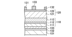
図1は、一実施形態に係る窒化物半導体素子の断面構成を示している。本実施形態の窒化物半導体素子は、図1に示すように主面が(111)面であるシリコン(Si)基板101の上に、窒化アルミニウム(AlN)からなる初期層102、及びAlGaNからなる中間層103が形成され、その上に歪み抑制層110及び動作層120が順次形成されている。初期層102は、SiとGaとの反応を抑制するために設けている。初期層102の膜厚が5nm程度よりも薄い場合にはその上に半導体層を鏡面成長させることが困難となる。膜厚が500nm程度よりも厚い場合にはその上に成長させた半導体層にクラックが多発する。中間層103は、例えば膜厚が40nmのAl0.3Ga0.7Nとすればよいが、Al組成は適宜変更してかまわない。中間層103は必要に応じて形成すればよく、初期層102の上に直接歪み抑制層110を形成してもよい。
FIG. 1 shows a cross-sectional configuration of a nitride semiconductor device according to an embodiment. As shown in FIG. 1, the nitride semiconductor device of this embodiment includes an
歪み抑制層110は、図2に示すように、順次形成されたGaNからなる第1のスペーサ層111、AlNからなる第2のスペーサ層112及び超格子層113とを有している。超格子層113は、AlGaNからなる第1の層113AとAlNからなる第2の層113Bとが交互に積層されている。
As shown in FIG. 2, the
動作層120は、歪み抑制層110側から順次形成されたGaNからなるチャネル層121とAlGaNからなるバリア層122とを有している。バリア層122の上には、互いに間隔をおいてソース電極131とドレイン電極132とが形成され、ソース電極131とドレイン電極132との間にはゲート電極133が形成されている。
The
次に、本実施形態の窒化物半導体素子により、基板及びその上に形成した半導体層の反りを低減できる原理について説明する。図3は、本実施形態の窒化物半導体素子の歪み抑制層110における歪みの状態を示している。図3において横軸は超格子層113の上面を0とした場合の深さを示しており、縦軸は結晶の歪み率を示している。歪み率が正の場合には圧縮歪みが生じており、歪み率が負の場合には伸張歪みが生じていることを示している。歪み率の測定には後方散乱電子回折測定法(Electron Back Scattering Diffraction:EBSD)を用いた。第1のスペーサ層111は厚さが約300nmのGaNとし、第2のスペーサ層112は、厚さが約20nmのAl0.3Ga0.7Nとした。超格子層113は、第1の層113Aを厚さが20nmのAl0.3Ga0.7Nとし、第2の層113Bを厚さが約3nmのAlNとし、交互に19層ずつ積層した。超格子層113の最下層は第1の層113Aであり、最上層は第2の層113Bとした。また、中間層103は、厚さが40nmのAl0.3Ga0.7Nとした。
Next, the principle that the warpage of the substrate and the semiconductor layer formed thereon can be reduced by the nitride semiconductor device of this embodiment will be described. FIG. 3 shows a state of strain in the
図3に示すように、中間層103には伸張歪みが加わっているが、GaNからなる第1のスペーサ層111において、歪みの方向が圧縮歪みに変化する。中間層103と第1のスペーサ層111との界面から40nm程度の位置において圧縮歪みが最も大きくなり、その後次第に小さくなる。AlNからなる第2のスペーサ層112において、歪みの方向は圧縮歪みから伸張歪みに急激に変化し、第2のスペーサ層112と超格子層113との界面近傍において最も伸張歪みが大きくなる。超格子層113において、伸張歪みの程度は小さくなるが伸張歪みを維持する。
As shown in FIG. 3, the
図3に示すように、第1のスペーサ層111において圧縮歪みを加え、第1のスペーサ層111と第2のスペーサ層112との界面付近において歪みの方向を急激に伸張歪みに変化させ、その上に弱い伸張歪みを有する超格子層を配置した場合には、反りを小さくできることを本願発明者らは見出した。このような現象が生じる原因は明確ではないが、圧縮歪みが加わる層と接して大きな伸張歪みが加わる層を形成することにより、圧縮歪みと伸張歪みとのバランスを取ることができるためであると考えられる。
As shown in FIG. 3, compressive strain is applied in the
第1のスペーサ層111が圧縮歪みを生じるようにするには、第1のスペーサ層111を格子定数が大きい材料により形成すればよい。また、第1のスペーサ層111と第2のスペーサ層112との界面付近において、歪み率を大きく変化させるには、第2のスペーサ層112の格子定数を小さくし且つ第1のスペーサ層111と第2のスペーサ層112との格子定数の差を大きくすればよい。従って、第1のスペーサ層111をAlを含まないGaNとし、第2のスペーサ層112をGaを含まないAlNとすることが好ましい。但し、第1のスペーサ層111と第2のスペーサ層112との格子定数の差を確保できれば、第1のスペーサ層111にAlが含まれていたり、第2のスペーサ層112にGaが含まれていたりしてもかまわない。この場合には、第1のスペーサ層111のAl組成を第2のスペーサ層112及び中間層103のAl組成よりも小さくする必要がある。また、第1のスペーサ層111の格子定数を大きくするためにInを加えることも可能である。但し、Inを添加する場合には、成長温度を低温としたり、水素を含まないキャリアガスを用いたりする必要がある。製造の容易さからみてGaNが最も好ましい。
In order to cause the
第1のスペーサ層111の膜厚は、圧縮歪みが加えられる膜厚であればよいが、歪みの変化が大きい部分ではばらつきが大きくなるので、40nm程度よりも厚くすることが好ましい。また、膜厚をあまり厚くすると、圧縮歪みを加える効果が小さくなり、膜厚が500nm程度において圧縮歪みが加わらなくなり、それ以上厚くすると逆に伸張歪みとなってしまう。このため、膜厚は500nm程度よりも小さくすることが好ましい。加えられる圧縮歪みの大きさ等を考えると100nm〜300nm程度とすることがさらに好ましい。
The film thickness of the
第2のスペーサ層112の膜厚は、第1のスペーサ層111により生じた圧縮歪みを打ち消し、伸張歪みが加わる厚さであればよい。図4は第2のスペーサ層112の膜厚と、基板の反りとの関係を示している。図4において横軸は第2のスペーサ層112の膜厚を示し、縦軸は基板の反りの大きさを示している。反りが正の値の場合は窒化物半導体層を形成した面が凹状に反ったいわゆる下に凸に反っていることを示し、負の値の場合には窒化物半導体層を形成した面が凸状に反ったいわゆる上に凸に反っていることを示している。第2のスペーサ層112が存在しない場合には、基板は大きく下に凸に反っている。図4に示すように第2のスペーサ層112を形成しても、第2のスペーサ層112の膜厚が薄い場合には、基板は下に凸に反っている。これは、第1のスペーサ層111による圧縮歪みの効果を打ち消すことがでないためであると考えられる。第2のスペーサ層112の膜厚が厚くなると、基板の反りは次第に小さくなる。一方、第2のスペーサ層112の膜厚が20nm程度よりも厚くなると上に凸の反りが生じる。これは、伸張歪みが大きくなりすぎるためであると考えられる。
The film thickness of the
基板の反りが150nmよりも大きい場合には、窒化物半導体層にクラックが生じたり、基板が割れたりする不具合が非常に生じやすくなる。このため、第2のスペーサ層112の膜厚は5nm以上且つ30nm以下程度の範囲とすればよい。また、基板の反りが80nmよりも大きいと、真空チャックにより基板を保持することが困難となり、生産性が低下する。このため、第2のスペーサ層112の膜厚は10nm以上且つ25nm以下程度とすることが好ましい。
When the warpage of the substrate is larger than 150 nm, a problem that the nitride semiconductor layer is cracked or the substrate is cracked is very likely to occur. Therefore, the thickness of the
超格子層113は、定法により求めた平均の格子定数が第1のスペーサ層111と第2のスペーサ層112との間の値となるようにすればよい。格子定数を第1のスペーサ層111と第2のスペーサ層112との間にできれば、第2のスペーサ層112の上に形成する層は、必ずしも超格子層である必要はない。但し、超格子層113を用いることにより、クラックの発生をより効果的に抑えることができる。また、歪み抑制層110全体の膜厚を厚くすることができるため、半導体素子の耐圧を向上させる効果が得られる。
The
第1の層113A及び第2の層113Bの膜厚は、それぞれ20nm〜30nm程度及び3nm〜6nm程度とすればよい。第1の層113A及び第2の層113Bをこれ以上厚くすると、超格子構造としてバランスが取れなくなり、基板が大きく下に凸に反ってしまう。特に、第2の層113Bの膜厚は第2のスペーサ層112よりも薄くすることが好ましい。
The film thicknesses of the
超格子層113は、最低限第1の層113Aを2層と第2の層113Bを1層とにより構成することができるが、適正な大きさの歪みを与えるために第1の層113A及び第2の層113Bはそれぞれ3層以上とすることが好ましい。積層数が多い方が超格子層113の膜厚が厚くなり、半導体素子の耐圧を向上させることができる。但し、第1の層113A及び第2の層113Bをそれぞれ160層以上積層した場合には基板が大きく下に凸に反ることが確認されている。また、積層数を多くすると結晶成長時間が長くなり、原料使用量が増大するため製造コストを上昇させることになる。現実的には第1の層113A及び第2の層113Bをそれぞれ50層以下とすることが好ましく、20層以下とすることがより好ましい。超格子層113の最下層は格子定数が大きい第1の層113Aであることが好ましい。格子定数が小さい第2の層113Bを最下層とした場合には、第2のスペーサ層112の膜厚を調整し、伸張歪みが大きくなりすぎないようにする必要がある。一方、超格子層113の最上層は、第1の層113Aであっても第2の層113Bであってもよい。
Although the
第1の層113Aと第2の層113Bとの格子定数の差は大きい方が好ましい。このため、第1の層113AをAlを含まないGaNとし、第2の層113BをGaを含まないAlNとすることが考えられる。しかし、第1の層113AをGaNとした場合には、半導体素子の耐圧が低くなるということを本願発明者らは見出した。
The difference in lattice constant between the
図5は、第1の層113Aの組成と半導体素子の耐圧との関係を示している。図5において横軸はSi基板101とドレイン電極132との間の電圧を示し、縦軸はSi基板101とドレイン電極132との間の電流を示している。測定に用いた各試料は第1の層113Aの組成以外の構成を同一とした。図5に示すように、第1の層113AがGaNの場合には、基板−電極間に印加する電圧が400V程度において基板−電極間の電流が急激に立ち上がっており、半導体素子の耐圧は400V程度であった。一方、第1の層113AをAl0.2Ga0.8Nとした場合には、耐圧は1000V程度まで上昇した。さらにAlを増やし第1の層113AをAl0.5Ga0.5Nとした場合には耐圧は800V程度に低下した。第1の層113AをAlGaN層とした方が耐圧が高くなる理由は明確ではないが、第1の層113AをGaNよりも格子定数が小さいAlGaN層とした方が、歪み抑制層110の上に形成する動作層120の結晶性等が向上するのではないかと考えられる。従って、第1の層113AはAlxGa1-xNとし、半導体素子の耐圧を向上させるためにAl組成xは0よりも大きくすることが好ましい。また、第1のスペーサ層111がAlGaNである場合には、第1のスペーサ層111よりもAl組成が高く格子定数が小さい方が好ましい。但し、Al組成xを大きくしすぎると耐圧を向上させる効果が小さくなるだけでなく、反りを低減する効果も小さくなるのでAl組成xは0.5以下とすることが好ましく、Al組成xを0.2又は0.3程度とすることがより好ましい。必要とする耐圧が確保できるのであれば、さらにAl組成xを小さくしてもよい。また、第1の層113Aとの格子定数の差を大きくするため、第2の層113BはGaを含まないAlNとすることが好ましいが、第1の層113Aよりも格子定数が小さいAlyGa1-yN(x<y≦1)としてもよい。但し、超格子層113の平均の格子定数が第1のスペーサ層111よりも小さく且つ第2のスペーサ層112よりも大きくなるようにする。
FIG. 5 shows the relationship between the composition of the
アンドープのGaNからなるチャネル層121は、ある程度厚くした方が、表面の平坦性及び結晶特性を向上させることができる。また、半導体素子の耐圧も向上することができる。このため、膜厚を0.5μm程度よりも厚くすることが好ましい。但し、膜厚が6μmを越えると特に基板の端面部において異常成長が生じやすくなるので、6μm程度よりも薄くすることが好ましい。
The
バリア層122は、例えば厚さが25nmのAl0.25Ga0.75Nとすればよい。バリア層122のAl組成及び膜厚は必要に応じて適宜変更してかまわない。また、バリア層122にSi等の不純物を添加してもかまわない。また、Al組成及び不純物濃度等が異なる複数の層を含む積層構造としてもよい。
For example, the
ソース電極131及びドレイン電極132は、オーミック接合する金属を用いて形成すればよい。ソース電極131及びドレイン電極132がリセス構造を有していてもよい。ゲート電極133はショットキー接合する金属を用いて形成すればよい。ゲート電極133もリセス構造を有していてもよい。また、ゲート電極133とバリア層122との間のp型の窒化物半導体層が形成されており、ゲート電極133がp型の窒化物半導体層とオーミック接合した構成としてもよい。各電極は積層構造又は合金構造であってもよく、金属以外の材料からなる電極であってもよい。また、ソース電極131、ドレイン電極132及びゲート電極133に代えて、オーミック接合したアノード電極とショットキー接合したカソード電極とを形成すればショットキーバリアダイオードとすることができる。
The
初期層102、中間層103、歪み抑制層110及び動作層120は、有機金属化学気相堆積法(MOCVD法)等により形成すればよい、MOCVD法を用いる場合には、Gaの原料としてトリメチルガリウムを用い、Alの原料としてトリメチルアルミニウムを用い、Nの原料としてアンモニアを用いればよい。また、MOCVD法に代えてハイドライド気相成長法等を用いてもよい。
The
図6に示すように、歪み抑制層110を2組形成してもよい。歪み抑制層110を複数組形成することにより、基板の反りをさらに小さくすることが可能となる。また、チャネル層121とSi基板101との間隔が大きくなるため、半導体素子の耐圧をさらに向上させるという効果も得られる。歪み抑制層110は3組以上形成してもよい。但し、歪み抑制層を多くすると、結晶成長時間が長くなり、必要とする原料も増加するので製造コストが上昇する。また、各歪み抑制層110が完全に同じ構成である必要はない。
As shown in FIG. 6, two sets of strain suppression layers 110 may be formed. By forming a plurality of sets of the strain suppression layers 110, it is possible to further reduce the warpage of the substrate. Further, since the gap between the
以上のような構成の歪み抑制層の上に動作層を形成することにより、径が75mm(3インチ又は150mm(6インチ)以上のSi基板を用いた場合においても、基板の反りを小さく抑えることができる。これにより、クラックの発生及び基板の割れの発生等を抑制でき窒化物半導体素子の生産性を大きく向上することができる。また、径が小さいSi基板を用いた場合にも基板の反りが小さくなる効果が得られるため、生産性及び歩留まりを向上できる。さらに、半導体素子の耐圧を向上することもできるので、窒化物半導体を用いたパワーデバイス等に特に適した構造を実現できる。 By forming an operation layer on the strain suppression layer having the above-described configuration, even when a Si substrate having a diameter of 75 mm (3 inches or 150 mm (6 inches) or more) is used, the warpage of the substrate is suppressed to be small. As a result, the occurrence of cracks and the occurrence of cracks in the substrate can be suppressed, and the productivity of the nitride semiconductor device can be greatly improved, and even when a Si substrate having a small diameter is used, the warpage of the substrate can be improved. As a result, the productivity and yield can be improved, and the breakdown voltage of the semiconductor element can be improved, so that a structure particularly suitable for a power device using a nitride semiconductor can be realized.
本発明に係る窒化物半導体素子は、Si基板の上に形成した窒化物半導体素子の生産性及び動作特性を向上させることができ、特にパワーデバイス等の窒化物半導体素子として有用である。 The nitride semiconductor device according to the present invention can improve the productivity and operating characteristics of a nitride semiconductor device formed on a Si substrate, and is particularly useful as a nitride semiconductor device such as a power device.
101 Si基板
102 初期層
103 中間層
110 歪み抑制層
111 第1のスペーサ層
112 第2のスペーサ層
113 超格子層
113A 第1の層
113B 第2の層
120 動作層
121 チャネル層
122 バリア層
131 ソース電極
132 ドレイン電極
133 ゲート電極
101
Claims (20)
前記シリコン基板の上に形成された初期層と、
前記初期層の上に形成された中間層と、
前記中間層の上に形成された歪み抑制層と、
前記歪み抑制層の上に形成された動作層とを備え、
前記歪み抑制層は、
第1の窒化物半導体からなる第1のスペーサ層と、
前記第1のスペーサ層の上に接して形成され、前記第1の窒化物半導体よりも格子定数が小さい第2の窒化物半導体からなる第2のスペーサ層と、
前記第2のスペーサ層の上に接して形成され、第3の窒化物半導体からなる第1の層及び前記第3の窒化物半導体よりも格子定数が小さい第4の窒化物半導体からなる第2の層が交互に積層された超格子層とを有し、
前記超格子層は、平均の格子定数が前記第1のスペーサ層の格子定数よりも小さく且つ前記第2のスペーサ層の格子定数よりも大きく、
前記第2のスペーサ層は、前記第1のスペーサ層側において圧縮歪みを有し、前記超格子層側において伸張歪みを有し、
前記第1のスペーサ層のAl組成は、前記第2のスペーサ層及び前記中間層のAl組成よりも小さいことを特徴とする窒化物半導体素子。 A silicon substrate;
An initial layer formed on the silicon substrate ;
An intermediate layer formed on the initial layer;
A strain suppression layer formed on the intermediate layer ;
An operation layer formed on the strain suppression layer,
The strain suppression layer is
A first spacer layer made of a first nitride semiconductor;
A second spacer layer made of a second nitride semiconductor formed on and in contact with the first spacer layer and having a smaller lattice constant than the first nitride semiconductor;
A first layer formed on and in contact with the second spacer layer and made of a third nitride semiconductor and a second nitride semiconductor made of a fourth nitride semiconductor having a lattice constant smaller than that of the third nitride semiconductor. A superlattice layer in which the layers are alternately stacked,
The superlattice layer has an average lattice constant smaller than that of the first spacer layer and larger than that of the second spacer layer,
Said second spacer layer, said has a compressive strain in the first spacer layer side, have a tensile strain in the superlattice layer side,
The Al composition of the first spacer layer, said second spacer layer and the nitride semiconductor device characterized and smaller this than Al composition of the intermediate layer.
前記第2の層は、AlyGa1-yN(x<y≦1)からなることを特徴とする請求項1〜6のいずれか1項に記載の窒化物半導体素子。 The first layer is made of Al x Ga 1-x N,
The second layer, Al y Ga 1-y N (x <y ≦ 1) nitride semiconductor device according to any one of claims 1 to 6, characterized in that it consists of.
前記第2の層の膜厚は、3nm以上、6nm以下であることを特徴とする請求項1〜12のいずれか1項に記載の窒化物半導体素子。 The film thickness of the first layer is 20 nm or more and 30 nm or less,
The thickness of the second layer, 3 nm or more, the nitride semiconductor device according to any one of claims 1 to 12, characterized in that it is 6nm or less.
The nitride semiconductor device according to any one of claims 1 to 15, characterized in that a diode.
Priority Applications (3)
| Application Number | Priority Date | Filing Date | Title |
|---|---|---|---|
| JP2010089842A JP5689245B2 (en) | 2010-04-08 | 2010-04-08 | Nitride semiconductor device |
| US12/961,134 US8405067B2 (en) | 2010-04-08 | 2010-12-06 | Nitride semiconductor element |
| CN2011100420786A CN102214701A (en) | 2010-04-08 | 2011-02-17 | Nitride semiconductor element |
Applications Claiming Priority (1)
| Application Number | Priority Date | Filing Date | Title |
|---|---|---|---|
| JP2010089842A JP5689245B2 (en) | 2010-04-08 | 2010-04-08 | Nitride semiconductor device |
Publications (3)
| Publication Number | Publication Date |
|---|---|
| JP2011222722A JP2011222722A (en) | 2011-11-04 |
| JP2011222722A5 JP2011222722A5 (en) | 2013-01-31 |
| JP5689245B2 true JP5689245B2 (en) | 2015-03-25 |
Family
ID=44745926
Family Applications (1)
| Application Number | Title | Priority Date | Filing Date |
|---|---|---|---|
| JP2010089842A Active JP5689245B2 (en) | 2010-04-08 | 2010-04-08 | Nitride semiconductor device |
Country Status (3)
| Country | Link |
|---|---|
| US (1) | US8405067B2 (en) |
| JP (1) | JP5689245B2 (en) |
| CN (1) | CN102214701A (en) |
Families Citing this family (8)
| Publication number | Priority date | Publication date | Assignee | Title |
|---|---|---|---|---|
| CN102870195A (en) * | 2010-04-28 | 2013-01-09 | 日本碍子株式会社 | Epitaxial substrate and process for producing epitaxial substrate |
| KR20120027988A (en) * | 2010-09-14 | 2012-03-22 | 삼성엘이디 주식회사 | Gallium nitride based semiconductor device and method of manufacturing the same |
| US9312436B2 (en) * | 2011-05-16 | 2016-04-12 | Kabushiki Kaisha Toshiba | Nitride semiconductor device, nitride semiconductor wafer, and method for manufacturing nitride semiconductor layer |
| JP5228122B1 (en) | 2012-03-08 | 2013-07-03 | 株式会社東芝 | Nitride semiconductor device and nitride semiconductor wafer |
| JP6165884B2 (en) * | 2013-01-31 | 2017-07-19 | オスラム オプト セミコンダクターズ ゲゼルシャフト ミット ベシュレンクテル ハフツングOsram Opto Semiconductors GmbH | Semiconductor laminate and method for producing semiconductor laminate |
| JP2015192004A (en) * | 2014-03-28 | 2015-11-02 | 国立大学法人 名古屋工業大学 | Mis type normally-off hemt element of recess structure having drain current density/transconductance improved greatly |
| JP6796467B2 (en) * | 2016-11-30 | 2020-12-09 | 住友化学株式会社 | Semiconductor substrate |
| CN115084293B (en) * | 2022-05-11 | 2024-07-12 | 中山大学 | Heterojunction photoelectric detector |
Family Cites Families (15)
| Publication number | Priority date | Publication date | Assignee | Title |
|---|---|---|---|---|
| JP3778765B2 (en) | 2000-03-24 | 2006-05-24 | 三洋電機株式会社 | Nitride-based semiconductor device and manufacturing method thereof |
| JP4554803B2 (en) * | 2000-12-04 | 2010-09-29 | 独立行政法人理化学研究所 | Low dislocation buffer, method for producing the same, and device having low dislocation buffer |
| US7115896B2 (en) | 2002-12-04 | 2006-10-03 | Emcore Corporation | Semiconductor structures for gallium nitride-based devices |
| JP4725763B2 (en) * | 2003-11-21 | 2011-07-13 | サンケン電気株式会社 | Method for manufacturing plate-like substrate for forming semiconductor element |
| JP4379305B2 (en) * | 2004-11-09 | 2009-12-09 | サンケン電気株式会社 | Semiconductor device |
| JP2007088426A (en) | 2005-08-25 | 2007-04-05 | Furukawa Electric Co Ltd:The | Semiconductor electronic device |
| JP2007250721A (en) * | 2006-03-15 | 2007-09-27 | Matsushita Electric Ind Co Ltd | Nitride semiconductor field effect transistor structure |
| JP4897956B2 (en) * | 2006-12-20 | 2012-03-14 | 古河電気工業株式会社 | Semiconductor electronic device |
| JP5224311B2 (en) * | 2007-01-05 | 2013-07-03 | 古河電気工業株式会社 | Semiconductor electronic device |
| JP5309452B2 (en) | 2007-02-28 | 2013-10-09 | サンケン電気株式会社 | Semiconductor wafer, semiconductor device, and manufacturing method |
| JP2009010142A (en) * | 2007-06-27 | 2009-01-15 | Toyoda Gosei Co Ltd | Hfet made of group-iii nitride semiconductor, and manufacturing method thereof |
| JP4592742B2 (en) * | 2007-12-27 | 2010-12-08 | Dowaエレクトロニクス株式会社 | Semiconductor material, method for manufacturing semiconductor material, and semiconductor element |
| US8067787B2 (en) | 2008-02-07 | 2011-11-29 | The Furukawa Electric Co., Ltd | Semiconductor electronic device |
| JP5053220B2 (en) * | 2008-09-30 | 2012-10-17 | 古河電気工業株式会社 | Semiconductor electronic device and method for manufacturing semiconductor electronic device |
| US8847203B2 (en) * | 2009-11-04 | 2014-09-30 | Dowa Electronics Materials Co, Ltd. | Group III nitride epitaxial laminate substrate |
-
2010
- 2010-04-08 JP JP2010089842A patent/JP5689245B2/en active Active
- 2010-12-06 US US12/961,134 patent/US8405067B2/en active Active
-
2011
- 2011-02-17 CN CN2011100420786A patent/CN102214701A/en active Pending
Also Published As
| Publication number | Publication date |
|---|---|
| US8405067B2 (en) | 2013-03-26 |
| JP2011222722A (en) | 2011-11-04 |
| CN102214701A (en) | 2011-10-12 |
| US20110248241A1 (en) | 2011-10-13 |
Similar Documents
| Publication | Publication Date | Title |
|---|---|---|
| JP5689245B2 (en) | Nitride semiconductor device | |
| JP5785103B2 (en) | Epitaxial wafers for heterojunction field effect transistors. | |
| JP5804768B2 (en) | Semiconductor device and manufacturing method thereof | |
| JP5891650B2 (en) | Compound semiconductor device and manufacturing method thereof | |
| JP5749580B2 (en) | Semiconductor device and manufacturing method of semiconductor device | |
| JP5100427B2 (en) | Semiconductor electronic device | |
| JP2013235873A (en) | Semiconductor device and method of manufacturing the same | |
| TW201318202A (en) | Iii nitride epitaxial substrate and method for manufacturing same | |
| US20150340230A1 (en) | Iii nitride epitaxial substrate and method of producing the same | |
| WO2011024754A1 (en) | Group iii nitride laminated semiconductor wafer and group iii nitride semiconductor device | |
| JP5543866B2 (en) | Group III nitride epitaxial substrate | |
| WO2016084311A1 (en) | Epitaxial wafer, semiconductor element, epitaxial wafer manufacturing method, and semiconductor element manufacturing method | |
| JP2018037435A (en) | Semiconductor device | |
| JP2019169572A (en) | Semiconductor device and manufacturing method thereof | |
| JP4888537B2 (en) | Group III nitride semiconductor laminated wafer and group III nitride semiconductor device | |
| JP6173493B2 (en) | Epitaxial substrate for semiconductor device and method of manufacturing the same | |
| JP2013145782A (en) | Epitaxial wafer for hetero-junction field effect transistor | |
| JP2016195241A (en) | Nitride semiconductor substrate | |
| JP2016062987A (en) | Semiconductor device and manufacturing method of the same | |
| JP6142893B2 (en) | Compound semiconductor device and manufacturing method thereof | |
| US20160293710A1 (en) | Nitride semiconductor substrate | |
| JP2015103665A (en) | Nitride semiconductor epitaxial wafer and nitride semiconductor | |
| WO2014192227A1 (en) | Semiconductor substrate, semiconductor device, and semiconductor device manufacturing method | |
| JP2012064977A (en) | Group iii nitride semiconductor stacked wafer and group iii nitride semiconductor device | |
| JP6029538B2 (en) | Semiconductor device |
Legal Events
| Date | Code | Title | Description |
|---|---|---|---|
| A521 | Request for written amendment filed |
Free format text: JAPANESE INTERMEDIATE CODE: A523 Effective date: 20121211 |
|
| A621 | Written request for application examination |
Free format text: JAPANESE INTERMEDIATE CODE: A621 Effective date: 20121211 |
|
| RD02 | Notification of acceptance of power of attorney |
Free format text: JAPANESE INTERMEDIATE CODE: A7422 Effective date: 20121211 |
|
| A977 | Report on retrieval |
Free format text: JAPANESE INTERMEDIATE CODE: A971007 Effective date: 20131216 |
|
| A131 | Notification of reasons for refusal |
Free format text: JAPANESE INTERMEDIATE CODE: A131 Effective date: 20140204 |
|
| A521 | Request for written amendment filed |
Free format text: JAPANESE INTERMEDIATE CODE: A523 Effective date: 20140403 |
|
| A131 | Notification of reasons for refusal |
Free format text: JAPANESE INTERMEDIATE CODE: A131 Effective date: 20140819 |
|
| A521 | Request for written amendment filed |
Free format text: JAPANESE INTERMEDIATE CODE: A523 Effective date: 20141014 |
|
| TRDD | Decision of grant or rejection written | ||
| A01 | Written decision to grant a patent or to grant a registration (utility model) |
Free format text: JAPANESE INTERMEDIATE CODE: A01 Effective date: 20150106 |
|
| A61 | First payment of annual fees (during grant procedure) |
Free format text: JAPANESE INTERMEDIATE CODE: A61 Effective date: 20150128 |
|
| R151 | Written notification of patent or utility model registration |
Ref document number: 5689245 Country of ref document: JP Free format text: JAPANESE INTERMEDIATE CODE: R151 |