JP5676413B2 - Power semiconductor device - Google Patents
Power semiconductor device Download PDFInfo
- Publication number
- JP5676413B2 JP5676413B2 JP2011236784A JP2011236784A JP5676413B2 JP 5676413 B2 JP5676413 B2 JP 5676413B2 JP 2011236784 A JP2011236784 A JP 2011236784A JP 2011236784 A JP2011236784 A JP 2011236784A JP 5676413 B2 JP5676413 B2 JP 5676413B2
- Authority
- JP
- Japan
- Prior art keywords
- power semiconductor
- die pad
- lead
- lead frame
- semiconductor device
- Prior art date
- Legal status (The legal status is an assumption and is not a legal conclusion. Google has not performed a legal analysis and makes no representation as to the accuracy of the status listed.)
- Active
Links
- 239000004065 semiconductor Substances 0.000 title claims description 300
- 238000005452 bending Methods 0.000 claims description 60
- 238000000034 method Methods 0.000 claims description 38
- 238000004519 manufacturing process Methods 0.000 claims description 28
- 230000008569 process Effects 0.000 claims description 24
- 239000011347 resin Substances 0.000 claims description 23
- 229920005989 resin Polymers 0.000 claims description 23
- 230000005855 radiation Effects 0.000 claims description 12
- 239000000463 material Substances 0.000 claims description 11
- HBMJWWWQQXIZIP-UHFFFAOYSA-N silicon carbide Chemical compound [Si+]#[C-] HBMJWWWQQXIZIP-UHFFFAOYSA-N 0.000 claims description 4
- JMASRVWKEDWRBT-UHFFFAOYSA-N Gallium nitride Chemical compound [Ga]#N JMASRVWKEDWRBT-UHFFFAOYSA-N 0.000 claims description 2
- 229910003460 diamond Inorganic materials 0.000 claims description 2
- 239000010432 diamond Substances 0.000 claims description 2
- 229910010271 silicon carbide Inorganic materials 0.000 claims description 2
- 229910002601 GaN Inorganic materials 0.000 claims 1
- 238000007789 sealing Methods 0.000 description 44
- 230000035882 stress Effects 0.000 description 18
- 230000000694 effects Effects 0.000 description 10
- 238000010586 diagram Methods 0.000 description 7
- 230000017525 heat dissipation Effects 0.000 description 7
- 238000012986 modification Methods 0.000 description 7
- 230000004048 modification Effects 0.000 description 7
- 239000000853 adhesive Substances 0.000 description 6
- 230000001070 adhesive effect Effects 0.000 description 6
- 238000001816 cooling Methods 0.000 description 6
- 239000010949 copper Substances 0.000 description 6
- 239000002184 metal Substances 0.000 description 6
- 229910052751 metal Inorganic materials 0.000 description 6
- 238000012546 transfer Methods 0.000 description 6
- XUIMIQQOPSSXEZ-UHFFFAOYSA-N Silicon Chemical compound [Si] XUIMIQQOPSSXEZ-UHFFFAOYSA-N 0.000 description 5
- 229910052710 silicon Inorganic materials 0.000 description 5
- 239000010703 silicon Substances 0.000 description 5
- 238000005530 etching Methods 0.000 description 4
- 229910000679 solder Inorganic materials 0.000 description 4
- RYGMFSIKBFXOCR-UHFFFAOYSA-N Copper Chemical compound [Cu] RYGMFSIKBFXOCR-UHFFFAOYSA-N 0.000 description 3
- 238000004891 communication Methods 0.000 description 3
- 229910052802 copper Inorganic materials 0.000 description 3
- 230000002093 peripheral effect Effects 0.000 description 3
- 238000003825 pressing Methods 0.000 description 3
- 238000004080 punching Methods 0.000 description 3
- 230000008859 change Effects 0.000 description 2
- 238000005520 cutting process Methods 0.000 description 2
- 150000002739 metals Chemical class 0.000 description 2
- 238000012545 processing Methods 0.000 description 2
- 238000003466 welding Methods 0.000 description 2
- -1 Al wire and Cu wire Chemical class 0.000 description 1
- 229910006913 SnSb Inorganic materials 0.000 description 1
- 238000013459 approach Methods 0.000 description 1
- 230000008901 benefit Effects 0.000 description 1
- 230000015572 biosynthetic process Effects 0.000 description 1
- 238000006073 displacement reaction Methods 0.000 description 1
- 230000001747 exhibiting effect Effects 0.000 description 1
- 239000007789 gas Substances 0.000 description 1
- 230000020169 heat generation Effects 0.000 description 1
- 238000005304 joining Methods 0.000 description 1
- 238000002844 melting Methods 0.000 description 1
- 230000008018 melting Effects 0.000 description 1
- 229910044991 metal oxide Inorganic materials 0.000 description 1
- 150000004706 metal oxides Chemical class 0.000 description 1
- 230000008646 thermal stress Effects 0.000 description 1
Images


Classifications
-
- H—ELECTRICITY
- H01—ELECTRIC ELEMENTS
- H01L—SEMICONDUCTOR DEVICES NOT COVERED BY CLASS H10
- H01L2224/00—Indexing scheme for arrangements for connecting or disconnecting semiconductor or solid-state bodies and methods related thereto as covered by H01L24/00
- H01L2224/01—Means for bonding being attached to, or being formed on, the surface to be connected, e.g. chip-to-package, die-attach, "first-level" interconnects; Manufacturing methods related thereto
- H01L2224/02—Bonding areas; Manufacturing methods related thereto
- H01L2224/04—Structure, shape, material or disposition of the bonding areas prior to the connecting process
- H01L2224/05—Structure, shape, material or disposition of the bonding areas prior to the connecting process of an individual bonding area
- H01L2224/0554—External layer
- H01L2224/0555—Shape
- H01L2224/05552—Shape in top view
- H01L2224/05554—Shape in top view being square
-
- H—ELECTRICITY
- H01—ELECTRIC ELEMENTS
- H01L—SEMICONDUCTOR DEVICES NOT COVERED BY CLASS H10
- H01L2224/00—Indexing scheme for arrangements for connecting or disconnecting semiconductor or solid-state bodies and methods related thereto as covered by H01L24/00
- H01L2224/01—Means for bonding being attached to, or being formed on, the surface to be connected, e.g. chip-to-package, die-attach, "first-level" interconnects; Manufacturing methods related thereto
- H01L2224/02—Bonding areas; Manufacturing methods related thereto
- H01L2224/04—Structure, shape, material or disposition of the bonding areas prior to the connecting process
- H01L2224/06—Structure, shape, material or disposition of the bonding areas prior to the connecting process of a plurality of bonding areas
- H01L2224/0601—Structure
- H01L2224/0603—Bonding areas having different sizes, e.g. different heights or widths
-
- H—ELECTRICITY
- H01—ELECTRIC ELEMENTS
- H01L—SEMICONDUCTOR DEVICES NOT COVERED BY CLASS H10
- H01L2224/00—Indexing scheme for arrangements for connecting or disconnecting semiconductor or solid-state bodies and methods related thereto as covered by H01L24/00
- H01L2224/01—Means for bonding being attached to, or being formed on, the surface to be connected, e.g. chip-to-package, die-attach, "first-level" interconnects; Manufacturing methods related thereto
- H01L2224/42—Wire connectors; Manufacturing methods related thereto
- H01L2224/47—Structure, shape, material or disposition of the wire connectors after the connecting process
- H01L2224/48—Structure, shape, material or disposition of the wire connectors after the connecting process of an individual wire connector
- H01L2224/4805—Shape
- H01L2224/4809—Loop shape
- H01L2224/48095—Kinked
- H01L2224/48096—Kinked the kinked part being in proximity to the bonding area on the semiconductor or solid-state body
-
- H—ELECTRICITY
- H01—ELECTRIC ELEMENTS
- H01L—SEMICONDUCTOR DEVICES NOT COVERED BY CLASS H10
- H01L2224/00—Indexing scheme for arrangements for connecting or disconnecting semiconductor or solid-state bodies and methods related thereto as covered by H01L24/00
- H01L2224/01—Means for bonding being attached to, or being formed on, the surface to be connected, e.g. chip-to-package, die-attach, "first-level" interconnects; Manufacturing methods related thereto
- H01L2224/42—Wire connectors; Manufacturing methods related thereto
- H01L2224/47—Structure, shape, material or disposition of the wire connectors after the connecting process
- H01L2224/48—Structure, shape, material or disposition of the wire connectors after the connecting process of an individual wire connector
- H01L2224/481—Disposition
- H01L2224/48135—Connecting between different semiconductor or solid-state bodies, i.e. chip-to-chip
- H01L2224/48137—Connecting between different semiconductor or solid-state bodies, i.e. chip-to-chip the bodies being arranged next to each other, e.g. on a common substrate
- H01L2224/48139—Connecting between different semiconductor or solid-state bodies, i.e. chip-to-chip the bodies being arranged next to each other, e.g. on a common substrate with an intermediate bond, e.g. continuous wire daisy chain
-
- H—ELECTRICITY
- H01—ELECTRIC ELEMENTS
- H01L—SEMICONDUCTOR DEVICES NOT COVERED BY CLASS H10
- H01L2224/00—Indexing scheme for arrangements for connecting or disconnecting semiconductor or solid-state bodies and methods related thereto as covered by H01L24/00
- H01L2224/01—Means for bonding being attached to, or being formed on, the surface to be connected, e.g. chip-to-package, die-attach, "first-level" interconnects; Manufacturing methods related thereto
- H01L2224/42—Wire connectors; Manufacturing methods related thereto
- H01L2224/47—Structure, shape, material or disposition of the wire connectors after the connecting process
- H01L2224/48—Structure, shape, material or disposition of the wire connectors after the connecting process of an individual wire connector
- H01L2224/481—Disposition
- H01L2224/48151—Connecting between a semiconductor or solid-state body and an item not being a semiconductor or solid-state body, e.g. chip-to-substrate, chip-to-passive
- H01L2224/48221—Connecting between a semiconductor or solid-state body and an item not being a semiconductor or solid-state body, e.g. chip-to-substrate, chip-to-passive the body and the item being stacked
- H01L2224/48245—Connecting between a semiconductor or solid-state body and an item not being a semiconductor or solid-state body, e.g. chip-to-substrate, chip-to-passive the body and the item being stacked the item being metallic
- H01L2224/48247—Connecting between a semiconductor or solid-state body and an item not being a semiconductor or solid-state body, e.g. chip-to-substrate, chip-to-passive the body and the item being stacked the item being metallic connecting the wire to a bond pad of the item
-
- H—ELECTRICITY
- H01—ELECTRIC ELEMENTS
- H01L—SEMICONDUCTOR DEVICES NOT COVERED BY CLASS H10
- H01L2224/00—Indexing scheme for arrangements for connecting or disconnecting semiconductor or solid-state bodies and methods related thereto as covered by H01L24/00
- H01L2224/01—Means for bonding being attached to, or being formed on, the surface to be connected, e.g. chip-to-package, die-attach, "first-level" interconnects; Manufacturing methods related thereto
- H01L2224/42—Wire connectors; Manufacturing methods related thereto
- H01L2224/47—Structure, shape, material or disposition of the wire connectors after the connecting process
- H01L2224/49—Structure, shape, material or disposition of the wire connectors after the connecting process of a plurality of wire connectors
- H01L2224/4901—Structure
- H01L2224/4903—Connectors having different sizes, e.g. different diameters
-
- H—ELECTRICITY
- H01—ELECTRIC ELEMENTS
- H01L—SEMICONDUCTOR DEVICES NOT COVERED BY CLASS H10
- H01L2224/00—Indexing scheme for arrangements for connecting or disconnecting semiconductor or solid-state bodies and methods related thereto as covered by H01L24/00
- H01L2224/01—Means for bonding being attached to, or being formed on, the surface to be connected, e.g. chip-to-package, die-attach, "first-level" interconnects; Manufacturing methods related thereto
- H01L2224/42—Wire connectors; Manufacturing methods related thereto
- H01L2224/47—Structure, shape, material or disposition of the wire connectors after the connecting process
- H01L2224/49—Structure, shape, material or disposition of the wire connectors after the connecting process of a plurality of wire connectors
- H01L2224/491—Disposition
- H01L2224/4911—Disposition the connectors being bonded to at least one common bonding area, e.g. daisy chain
- H01L2224/49111—Disposition the connectors being bonded to at least one common bonding area, e.g. daisy chain the connectors connecting two common bonding areas, e.g. Litz or braid wires
-
- H—ELECTRICITY
- H01—ELECTRIC ELEMENTS
- H01L—SEMICONDUCTOR DEVICES NOT COVERED BY CLASS H10
- H01L2224/00—Indexing scheme for arrangements for connecting or disconnecting semiconductor or solid-state bodies and methods related thereto as covered by H01L24/00
- H01L2224/01—Means for bonding being attached to, or being formed on, the surface to be connected, e.g. chip-to-package, die-attach, "first-level" interconnects; Manufacturing methods related thereto
- H01L2224/42—Wire connectors; Manufacturing methods related thereto
- H01L2224/47—Structure, shape, material or disposition of the wire connectors after the connecting process
- H01L2224/49—Structure, shape, material or disposition of the wire connectors after the connecting process of a plurality of wire connectors
- H01L2224/491—Disposition
- H01L2224/4912—Layout
- H01L2224/49171—Fan-out arrangements
-
- H—ELECTRICITY
- H01—ELECTRIC ELEMENTS
- H01L—SEMICONDUCTOR DEVICES NOT COVERED BY CLASS H10
- H01L2224/00—Indexing scheme for arrangements for connecting or disconnecting semiconductor or solid-state bodies and methods related thereto as covered by H01L24/00
- H01L2224/01—Means for bonding being attached to, or being formed on, the surface to be connected, e.g. chip-to-package, die-attach, "first-level" interconnects; Manufacturing methods related thereto
- H01L2224/42—Wire connectors; Manufacturing methods related thereto
- H01L2224/47—Structure, shape, material or disposition of the wire connectors after the connecting process
- H01L2224/49—Structure, shape, material or disposition of the wire connectors after the connecting process of a plurality of wire connectors
- H01L2224/491—Disposition
- H01L2224/4912—Layout
- H01L2224/49175—Parallel arrangements
-
- H—ELECTRICITY
- H01—ELECTRIC ELEMENTS
- H01L—SEMICONDUCTOR DEVICES NOT COVERED BY CLASS H10
- H01L2924/00—Indexing scheme for arrangements or methods for connecting or disconnecting semiconductor or solid-state bodies as covered by H01L24/00
- H01L2924/10—Details of semiconductor or other solid state devices to be connected
- H01L2924/102—Material of the semiconductor or solid state bodies
- H01L2924/1025—Semiconducting materials
- H01L2924/10251—Elemental semiconductors, i.e. Group IV
- H01L2924/10253—Silicon [Si]
-
- H—ELECTRICITY
- H01—ELECTRIC ELEMENTS
- H01L—SEMICONDUCTOR DEVICES NOT COVERED BY CLASS H10
- H01L2924/00—Indexing scheme for arrangements or methods for connecting or disconnecting semiconductor or solid-state bodies as covered by H01L24/00
- H01L2924/10—Details of semiconductor or other solid state devices to be connected
- H01L2924/11—Device type
- H01L2924/13—Discrete devices, e.g. 3 terminal devices
- H01L2924/1304—Transistor
- H01L2924/1305—Bipolar Junction Transistor [BJT]
- H01L2924/13055—Insulated gate bipolar transistor [IGBT]
-
- H—ELECTRICITY
- H01—ELECTRIC ELEMENTS
- H01L—SEMICONDUCTOR DEVICES NOT COVERED BY CLASS H10
- H01L2924/00—Indexing scheme for arrangements or methods for connecting or disconnecting semiconductor or solid-state bodies as covered by H01L24/00
- H01L2924/10—Details of semiconductor or other solid state devices to be connected
- H01L2924/11—Device type
- H01L2924/13—Discrete devices, e.g. 3 terminal devices
- H01L2924/1304—Transistor
- H01L2924/1306—Field-effect transistor [FET]
- H01L2924/13091—Metal-Oxide-Semiconductor Field-Effect Transistor [MOSFET]
Description
本発明は、リードフレームを用いた電力用半導体装置の構成に関する。 The present invention relates to the structure of the power semiconductor device using a lead frame.
半導体装置の中でも電力用半導体装置は、産業用機器から家電・情報端末まで幅広い機器の主電力(パワー)の制御に用いられ、とくに輸送機器等においては高い信頼性が求められている。また、近年、シリコン(Si)に代わる半導体材料として大電流を流すことができ、高効率が期待できるワイドバンドギャップ半導体材料である炭化珪素(SiC)が注目されている。一方、ワイドバンドギャップ半導体素子では、シリコンよりも高い150℃〜300℃の動作温度が想定され、大電流および高温に適したパッケージ形態も同時に求められている。 Among semiconductor devices, a power semiconductor device is used for controlling main power of a wide range of equipment from industrial equipment to home appliances and information terminals, and high reliability is particularly required for transportation equipment and the like. In recent years, silicon carbide (SiC), which is a wide band gap semiconductor material that can flow a large current and can be expected to be highly efficient, has attracted attention as a semiconductor material that can replace silicon (Si). On the other hand, a wide band gap semiconductor element is assumed to have an operating temperature of 150 ° C. to 300 ° C. higher than that of silicon, and a package form suitable for a large current and a high temperature is also required at the same time.
半導体装置に用いるリードフレームは、通常、1枚の板状部材からプレスでの打ち抜きや、エッチング等により、余分な分を除去することで平面上にパターン形成される。そして、機器の出力を制御するために用いられるパワーモジュール(電力用半導体装置)では、主電力を操作するパワー素子(電力用半導体素子)と、電力用半導体素子の動作を制御するための制御素子が、上述したリードフレームの所定位置(ダイパッド)に接合されている。発熱が大きな電力用半導体素子は、ヒートシンクを接続して外部に放熱をする必要があるが、制御素子にはその必要はない。しかし、上記のようなリードフレームに電力用半導体素子と制御素子が平面配置された場合、冷却の必要のない制御素子の部分まで面積を広げる必要があり、小型化の妨げとなっていた。 A lead frame used in a semiconductor device is usually patterned on a flat surface by removing excess portions from a single plate-like member by stamping or etching. In a power module (power semiconductor device) used to control the output of the device, a power element (power semiconductor element) for operating main power and a control element for controlling the operation of the power semiconductor element Is bonded to a predetermined position (die pad) of the lead frame described above. A power semiconductor element that generates a large amount of heat needs to be radiated to the outside by connecting a heat sink, but the control element does not have to. However, when the power semiconductor element and the control element are arranged in a plane on the lead frame as described above, it is necessary to increase the area to the part of the control element that does not require cooling, which hinders miniaturization.
そこで、電力用半導体素子と制御素子をそれぞれ別のリードフレーム内に配置し、電力用半導体素子と制御素子とが面内でオーバーラップするように階層化した半導体装置が提案されている(例えば、特許文献1参照。)。 Therefore, a semiconductor device has been proposed in which a power semiconductor element and a control element are arranged in separate lead frames, and the power semiconductor element and the control element are layered so as to overlap in a plane (for example, (See Patent Document 1).
一方、リードフレームを用いる半導体装置では、封止の際にリードフレームの両端を上下の金型で挟んで締めこむことによって、封止体内での部材の位置を固定する。そこで、上記のような2枚のリードフレームを用いた半導体装置を封止しようとすると、2枚のリードフレームを重ね合わせた部分が上下の金型に挟み込まれることになる。リードフレームの金型で締めこまれる部分には、平行する多数の切込みが形成されているので、重ね合わせによって金型内部から外部に連通する隙間が生じ、樹脂が漏れ出して十分な封止ができなくなる可能性があった。また、上記特許文献の別の実施の形態に示されているように、電力用半導体素子部分のリードフレームを一端側、制御素子のリードフレームを他端側で挟み込むようにした場合、隙間の発生は抑えられるが、部材を金型内でしっかりと固定することができず、製品にばらつきが生じる可能性があった。 On the other hand, in a semiconductor device using a lead frame, the position of the member in the sealed body is fixed by clamping the both ends of the lead frame between upper and lower molds at the time of sealing. Therefore, when a semiconductor device using two lead frames as described above is to be sealed, a portion where the two lead frames are overlapped is sandwiched between upper and lower molds. A lot of parallel cuts are formed in the portion of the lead frame that is tightened by the die, so that a gap that communicates from the inside of the die to the outside is created due to the overlap, and the resin leaks out to provide sufficient sealing There was a possibility of becoming impossible. Further, as shown in another embodiment of the above-mentioned patent document, when the lead frame of the power semiconductor element portion is sandwiched between one end side and the lead frame of the control element is sandwiched between the other end side, a gap is generated. However, the members could not be firmly fixed in the mold, and there was a possibility that the products varied.
本発明は、上記のような課題を解決するためになされたもので、小型で、信頼性の高い電力用半導体装置を得ることを目的としている。 The present invention has been made to solve the above-described problems, and an object of the present invention is to obtain a small-sized and highly reliable power semiconductor device.
本発明の電力用半導体装置は、略矩形板状をなし、主電力を制御する電力用半導体素子と前記電力用半導体素子を制御する制御信号を出力する制御素子とが厚み方向において段違いに配置されるとともに、前記矩形板状の対向する側面のそれぞれから並列する複数の端子が突出配置された電力用半導体装置を一枚のリードフレームを用いて製造する方法であって、前記1枚のリードフレームには、前記電力用半導体素子が接合される第1のダイパッドと、前記制御素子が接合される第2のダイパッドが、前記並列する複数の端子となるリードパターンとともに、前記リードパターンの延在方向におけるそれぞれ一端側の領域と他端側の領域で連なるように形成されているとともに、前記一端側の領域から前記他端側の領域にかけて延在する延在パターンが形成され、かつ、前記リードフレームの面に垂直な方向において前記第1のダイパッドに対して前記第2のダイパッドが上方に位置するように段差がつけられており、前記第1のダイパッドの一面に前記電力用半導体素子を接合するとともに、前記第2のダイパッドに前記制御素子を接合する工程と、前記リードフレームの面を保ったまま、前記延在パターンの所定部分を屈曲させ、前記リードフレームの面に垂直な方向から見たときに、前記制御素子を、前記電力用半導体素子にオーバーラップさせる工程と、前記第1のダイパッドの裏面に、放熱部材を接合する工程と、前記リードフレームを少なくとも外枠部分が露出した状態で上下の金型ではさみ、前記金型内に樹脂を流し込んで、前記放熱部材の放熱面を除いて当該電力用半導体装置を略矩形形状に封止する工程と、を含む電力用半導体装置の製造方法により製造した電力用半導体装置において、前記延在パターンにおける前記所定部分よりも前記一端側の部分と前記電力用半導体素子の制御電極とが配線部材で電気接続されるとともに、前記延在パターンにおける前記所定部分よりも前記他端側の部分と前記制御素子の制御信号を出力する電極とが配線部材で電気接続されていることを特徴とする。 The power semiconductor device of the present invention has a substantially rectangular plate shape, and a power semiconductor element for controlling main power and a control element for outputting a control signal for controlling the power semiconductor element are arranged in a stepwise manner in the thickness direction. And a method of manufacturing a power semiconductor device using a single lead frame in which a plurality of terminals juxtaposed from each of the opposing side surfaces of the rectangular plate are disposed. The first die pad to which the power semiconductor element is bonded and the second die pad to which the control element is bonded together with the lead pattern serving as the plurality of terminals arranged in parallel, and the extending direction of the lead pattern Are formed so as to be continuous with each other at one end side region and the other end side region, and extend from the one end side region to the other end side region. A step is formed so that the second die pad is positioned above the first die pad in a direction perpendicular to the surface of the lead frame, and a pattern is formed. Bonding the power semiconductor element to one surface and bonding the control element to the second die pad; and bending a predetermined portion of the extended pattern while maintaining the surface of the lead frame; A step of overlapping the control element with the power semiconductor element when viewed from a direction perpendicular to the surface of the frame, a step of bonding a heat radiating member to the back surface of the first die pad, and the lead frame Is sandwiched between the upper and lower molds with at least the outer frame part exposed, and the resin is poured into the mold to remove the heat dissipation surface of the heat dissipation member. In the power semiconductor device manufactured by the method of manufacturing the power semiconductor device including a step of sealing the use semiconductor device in a substantially rectangular shape, and said one end portion and the power than the predetermined portion of the extended pattern The wiring electrode is electrically connected to the control electrode of the semiconductor element for wiring, and the wiring member is electrically connected to the portion on the other end side than the predetermined portion in the extended pattern and the electrode for outputting the control signal of the control element. It is connected .
また、本発明の電力用半導体装置は、略矩形板状をなし、主電力を制御する電力用半導体素子と前記電力用半導体素子を制御する制御信号を出力する制御素子とが厚み方向において段違いに配置されるとともに、前記矩形板状の対向する側面のそれぞれから並列する複数の端子が突出配置された電力用半導体装置を一枚のリードフレームを用いて製造する方法であって、前記1枚のリードフレームには、前記電力用半導体素子が接合される第1のダイパッドと、前記制御素子が接合される第2のダイパッドが、前記並列する複数の端子となるリードパターンとともに、前記リードパターンの延在方向におけるそれぞれ一端側の領域と他端側の領域で連なるように形成されているとともに、前記一端側の領域から前記他端側の領域にかけて延在する延在パターンが形成され、かつ、前記リードフレームの面に垂直な方向において前記第1のダイパッドに対して前記第2のダイパッドが上方に位置するように段差がつけられており、前記第1のダイパッドの一面に前記電力用半導体素子を接合するとともに、前記第2のダイパッドに前記制御素子を接合する工程と、前記リードフレームの面を保ったまま、前記延在パターンの所定部分を屈曲させ、前記リードフレームの面に垂直な方向から見たときに、前記制御素子を、前記電力用半導体素子にオーバーラップさせる工程と、前記第1のダイパッドの裏面に、放熱部材を接合する工程と、前記リードフレームを少なくとも外枠部分が露出した状態で上下の金型ではさみ、前記金型内に樹脂を流し込んで、前記放熱部材の放熱面を除いて当該電力用半導体装置を略矩形形状に封止する工程と、を含む電力用半導体装置の製造方法により製造した電力用半導体装置において、前記リードフレームの前記一端側の領域、および前記他端側の領域には、前記リードパターンが並列する方向において、それぞれ前記第1のダイパッドおよび前記第2のダイパッドよりも外側に位置する第1の中継リードと第2の中継リードが形成されており、前記第1の中継リードと前記電力用半導体素子の制御電極、および、前記第2の中継リードと前記制御素子の制御信号を出力する電極とが、それぞれ配線部材で電気接続されているとともに、前記屈曲によって接近した前記第1の中継リードと前記第2の中継リードとが、配線部材で電気接続されていることを特徴とする。The power semiconductor device of the present invention has a substantially rectangular plate shape, and the power semiconductor element for controlling the main power and the control element for outputting a control signal for controlling the power semiconductor element are different in the thickness direction. A method of manufacturing a power semiconductor device using a single lead frame in which a plurality of terminals juxtaposed from each of the opposing sides of the rectangular plate are arranged to protrude. The lead frame includes a first die pad to which the power semiconductor element is bonded and a second die pad to which the control element is bonded together with the lead pattern serving as the plurality of terminals arranged in parallel, and an extension of the lead pattern. Each region is formed so as to be continuous at one end region and the other end region, and extends from the one end region to the other end region. And a step is provided so that the second die pad is positioned above the first die pad in a direction perpendicular to the surface of the lead frame. Bonding the power semiconductor element to one surface of the die pad, and bonding the control element to the second die pad, and bending a predetermined portion of the extended pattern while keeping the surface of the lead frame. A step of overlapping the control element with the power semiconductor element when viewed from a direction perpendicular to the surface of the lead frame, and a step of bonding a heat radiating member to the back surface of the first die pad; The lead frame is sandwiched between upper and lower molds with at least the outer frame portion exposed, resin is poured into the mold, and the heat radiating surface of the heat radiating member is removed. Sealing the power semiconductor device into a substantially rectangular shape, and a power semiconductor device manufactured by a method for manufacturing a power semiconductor device, the region on the one end side of the lead frame, and the other end side In the region, there are formed a first relay lead and a second relay lead that are positioned outside the first die pad and the second die pad, respectively, in the direction in which the lead patterns are arranged in parallel. 1 relay lead and the control electrode of the power semiconductor element, and the second relay lead and an electrode for outputting a control signal of the control element are electrically connected by a wiring member, respectively, and by bending The approaching first relay lead and the second relay lead are electrically connected by a wiring member.
また、本発明の電力用半導体装置は、略矩形板状をなし、主電力を制御する電力用半導体素子と前記電力用半導体素子を制御する制御信号を出力する制御素子とが厚み方向において段違いに配置されるとともに、前記矩形板状の対向する側面のそれぞれから並列する複数の端子が突出配置された電力用半導体装置を一枚のリードフレームを用いて製造する方法であって、前記1枚のリードフレームには、前記電力用半導体素子が接合される第1のダイパッドと、前記制御素子が接合される第2のダイパッドが、前記並列する複数の端子となるリードパターンとともに、前記リードパターンの延在方向におけるそれぞれ一端側の領域と他端側の領域で連なるように形成されているとともに、前記一端側の領域から前記他端側の領域にかけて延在する延在パターンが形成され、かつ、前記リードフレームの面に垂直な方向において前記第1のダイパッドに対して前記第2のダイパッドが上方に位置するように段差がつけられており、前記第1のダイパッドの一面に前記電力用半導体素子を接合するとともに、前記第2のダイパッドに前記制御素子を接合する工程と、前記リードフレームの面を保ったまま、前記延在パターンの所定部分を屈曲させ、前記リードフレームの面に垂直な方向から見たときに、前記制御素子を、前記電力用半導体素子にオーバーラップさせる工程と、前記第1のダイパッドの裏面に、放熱部材を接合する工程と、前記リードフレームを少なくとも外枠部分が露出した状態で上下の金型ではさみ、前記金型内に樹脂を流し込んで、前記放熱部材の放熱面を除いて当該電力用半導体装置を略矩形形状に封止する工程と、を含む電力用半導体装置の製造方法により製造した電力用半導体装置において、前記電力用半導体素子は、整流素子とスイッチング素子からなる2つの半導体素子を並列配置したものであり、前記リードフレームには、前記一端側の領域から前記他端側の領域に達するとともに、前記他端側の端部に所定の大きさのバス部を有するバスパターンが形成されており、前記バスパターンの前記バス部以外の部分の折り曲げによって、前記バス部を前記2つの半導体素子にオーバーラップさせて、前記2つの半導体素子間が電気接続されているとともに、前記屈曲によって接近した前記電力用半導体素子の制御電極と前記制御素子の制御信号を出力する電極とが配線部材で電気接続されていることを特徴とする。The power semiconductor device of the present invention has a substantially rectangular plate shape, and the power semiconductor element for controlling the main power and the control element for outputting a control signal for controlling the power semiconductor element are different in the thickness direction. A method of manufacturing a power semiconductor device using a single lead frame in which a plurality of terminals juxtaposed from each of the opposing sides of the rectangular plate are arranged to protrude. The lead frame includes a first die pad to which the power semiconductor element is bonded and a second die pad to which the control element is bonded together with the lead pattern serving as the plurality of terminals arranged in parallel, and an extension of the lead pattern. Each region is formed so as to be continuous at one end region and the other end region, and extends from the one end region to the other end region. And a step is provided so that the second die pad is positioned above the first die pad in a direction perpendicular to the surface of the lead frame. Bonding the power semiconductor element to one surface of the die pad, and bonding the control element to the second die pad, and bending a predetermined portion of the extended pattern while keeping the surface of the lead frame. A step of overlapping the control element with the power semiconductor element when viewed from a direction perpendicular to the surface of the lead frame, and a step of bonding a heat radiating member to the back surface of the first die pad; The lead frame is sandwiched between upper and lower molds with at least the outer frame portion exposed, resin is poured into the mold, and the heat radiating surface of the heat radiating member is removed. Sealing the power semiconductor device into a substantially rectangular shape, wherein the power semiconductor element includes two rectifying elements and a switching element. A semiconductor element is arranged in parallel, and the lead frame has a bus portion having a predetermined size at the other end side from the one end side region to the other end side region. A pattern is formed, the bus part is overlapped with the two semiconductor elements by bending a part other than the bus part of the bus pattern, and the two semiconductor elements are electrically connected; A control electrode of the power semiconductor element approaching by the bending and an electrode for outputting a control signal of the control element are electrically connected by a wiring member. And features.
また、本発明の電力用半導体装置は、略矩形板状をなし、主電力を制御する電力用半導体素子と前記電力用半導体素子を制御する制御信号を出力する制御素子とが厚み方向において段違いに配置されるとともに、前記矩形板状の対向する側面のそれぞれから並列する複数の端子が突出配置された電力用半導体装置を一枚のリードフレームを用いて製造する方法であって、前記1枚のリードフレームには、前記電力用半導体素子が接合される第1のダイパッドと、前記制御素子が接合される第2のダイパッドが、前記並列する複数の端子となるリードパターンとともに、前記リードパターンの延在方向におけるそれぞれ一端側の領域と他端側の領域で連なるように形成されているとともに、前記一端側の領域から前記他端側の領域にかけて延在する延在パターンが形成され、かつ、前記リードフレームの面に垂直な方向において前記第1のダイパッドに対して前記第2のダイパッドが上方に位置するように段差がつけられており、前記第1のダイパッドの一面に前記電力用半導体素子を接合するとともに、前記第2のダイパッドに前記制御素子を接合する工程と、前記リードフレームの面を保ったまま、前記延在パターンの所定部分を屈曲させ、前記リードフレームの面に垂直な方向から見たときに、前記制御素子を、前記電力用半導体素子にオーバーラップさせる工程と、前記第1のダイパッドの裏面に、放熱部材を接合する工程と、前記リードフレームを少なくとも外枠部分が露出した状態で上下の金型ではさみ、前記金型内に樹脂を流し込んで、前記放熱部材の放熱面を除いて当該電力用半導体装置を略矩形形状に封止する工程と、を含む電力用半導体装置の製造方法により製造した電力用半導体装置において、前記延在パターンの所定部分には、前記リードパターンが並列する方向において向きが異なる複数の切欠きが前記延在方向の異なる位置に設けられ、前記複数の切欠きを開くことにより、前記所定部分が前記リードパターンの面に平行な方向で屈曲していることを特徴とする。The power semiconductor device of the present invention has a substantially rectangular plate shape, and the power semiconductor element for controlling the main power and the control element for outputting a control signal for controlling the power semiconductor element are different in the thickness direction. A method of manufacturing a power semiconductor device using a single lead frame in which a plurality of terminals juxtaposed from each of the opposing sides of the rectangular plate are arranged to protrude. The lead frame includes a first die pad to which the power semiconductor element is bonded and a second die pad to which the control element is bonded together with the lead pattern serving as the plurality of terminals arranged in parallel, and an extension of the lead pattern. Each region is formed so as to be continuous at one end region and the other end region, and extends from the one end region to the other end region. And a step is provided so that the second die pad is positioned above the first die pad in a direction perpendicular to the surface of the lead frame. Bonding the power semiconductor element to one surface of the die pad, and bonding the control element to the second die pad, and bending a predetermined portion of the extended pattern while keeping the surface of the lead frame. A step of overlapping the control element with the power semiconductor element when viewed from a direction perpendicular to the surface of the lead frame, and a step of bonding a heat radiating member to the back surface of the first die pad; The lead frame is sandwiched between upper and lower molds with at least the outer frame portion exposed, resin is poured into the mold, and the heat radiating surface of the heat radiating member is removed. And sealing the power semiconductor device into a substantially rectangular shape. The power semiconductor device manufactured by the method for manufacturing a power semiconductor device includes the lead pattern being parallel to the predetermined portion of the extended pattern. A plurality of notches having different orientations in the direction are provided at different positions in the extending direction, and the predetermined portions are bent in a direction parallel to the surface of the lead pattern by opening the plurality of notches. It is characterized by.
本発明の電力用半導体装置によれば、1枚のリードフレームを用いて電力回路と制御回路が段違いに形成された電力用半導体装置を構成するようにしたので、小型で、信頼性の高い電力用半導体装置を得ることができる。 According to the power semiconductor device of the present invention, the power semiconductor device in which the power circuit and the control circuit are formed in different stages using one lead frame is configured, so that the power semiconductor device is small and has high reliability. A semiconductor device can be obtained.
実施の形態1.
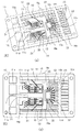
図1〜図4は、本発明の実施の形態1にかかる電力用半導体装置の製造方法および電力用半導体装置の構成を説明するためのもので、図1は電力用半導体装置を構成するためのリードフレームに半導体素子を接合し、配線部材を接続した状態の斜視図(図1(a))と上面図(図1(b))、図2はリードフレームに半導体素子が実装され、さらに、オーバーラップのための曲げ加工を施したトランスファモールドによる封止工程直前の状態の斜視図(図2(a))と上面図(図2(b))、図3は電力用半導体装置の製造方法を説明するためのフローチャート、図4は電力用半導体装置の構成を説明するための上面図(図4(a))と、上面図におけるB−B線による断面のうち、封止部材を除いて説明対象部分を抜き出した部分を示す断面図(図4(b))と、上面図におけるC−C線による断面のうち、封止部材を除いて説明対象部分を抜き出した部分を示す断面図(図4(c))である。また、図5は、本実施の形態の変形例にかかる電力用半導体装置を説明するためのもので、図5(a)は電力用半導体装置を構成するためのリードフレームに半導体素子を接合し、配線部材を接続した状態の斜視図、図5(b)は電力用半導体装置を構成するためのリードフレームに半導体素子が実装され、さらに、オーバーラップのための曲げ加工を施したトランスファモールドによる封止工程直前の状態の斜視図である。
1 to 4 are diagrams for explaining a method of manufacturing a power semiconductor device and a configuration of the power semiconductor device according to the first embodiment of the present invention. FIG. 1 is a diagram for configuring the power semiconductor device. A perspective view (FIG. 1 (a)) and a top view (FIG. 1 (b)) of a state in which a semiconductor element is joined to a lead frame and a wiring member is connected, FIG. 2 shows a semiconductor element mounted on the lead frame, A perspective view (FIG. 2 (a)) and a top view (FIG. 2 (b)) of a state immediately before a sealing process by a transfer mold subjected to bending for overlapping, FIG. 3 is a method for manufacturing a power semiconductor device FIG. 4 is a top view for explaining the configuration of the power semiconductor device (FIG. 4A), and a cross section taken along line BB in the top view, excluding the sealing member. Break indicating the part where the explanation target part was extracted Figure a (FIG. 4 (b)), among the section along the line C-C in top view, a sectional view showing a portion of an extracted description target portion except for the sealing member (FIG. 4 (c)). FIG. 5 is a diagram for explaining a power semiconductor device according to a modification of the present embodiment. FIG. 5A shows a semiconductor element bonded to a lead frame for constituting the power semiconductor device. FIG. 5B is a perspective view of a state in which wiring members are connected, and FIG. 5B is a transfer mold in which a semiconductor element is mounted on a lead frame for constituting a power semiconductor device, and further bent for overlap. It is a perspective view of the state just before a sealing process.
本実施の形態にかかる電力用半導体装置の構成と製造方法について図に基づいて説明する。
電力用半導体装置の電力回路を構成するためのリードフレーム10は、1枚の銅板を打ち抜いて平面状のパターンを形成したもので、図1に示すように、枠体15の内側の領域のうち、屈曲予定領域Rbより図中右側の領域が制御回路を形成するためのパターン、屈曲予定領域Rbよりも左側の領域が電力回路を形成するためのパターンである。制御回路を形成するパターンには、制御回路と電力回路を結ぶ方向(給電方向と称す)において延在するように、複数のリードパターン12tと、複数のリードパターン12iとが、タイバー16cを介して連なるとともに、それぞれ並行に形成されている。後の工程でタイバー16c部分を切り離し、枠体15を除去することにより、外部端子となるリードパターン12tのそれぞれと、内部配線部材となるリードパターン12iのそれぞれとが、それぞれ一連の制御リード12として機能する。そして、リードパターン12iのうち、ひとつのリードパターン12iの先端には、制御素子23である半導体の集積回路23を接合するためのダイパッド12dが形成されている。
The configuration and manufacturing method of the power semiconductor device according to the present embodiment will be described with reference to the drawings.
A
電力回路を形成するパターンにも、制御回路と同様に、後に外部端子となる複数のリードパターン11tと、内部配線部材となる複数のリードパターン11iとが給電方向において延在し、タイバー16pを介して連なるとともに、それぞれ並行に形成されている。リードパターン11iと11tのそれぞれも、後の工程でタイバー16p部分を切り離し、枠体15を除去することにより、それぞれ一連のパワーリード11として機能する。そして、リードパターン11iのうち、ひとつのリードパターン11iの先端には、電力用半導体素子として使用する整流素子であるダイオード21、スイッチング素子であるIGBT(Insulated Gate Bipolar Transistor)22を接合するためのダイパッド11dが
段差部11uを介して形成されている。
Similarly to the control circuit, a plurality of
さらに、枠体15の内側のうち、リードパターン11tおよびリードパターン12tが並ぶ方向(面方向における給電方向に垂直な方向:並列方向と称する)の最外側には、電力回路側から制御回路にわたって延在する共通リード13が形成されている。この共通リード13は、2つのタイバー16c、16p間を給電方向に延在するように形成されており、屈曲予定領域Rbよりも制御回路側の部分には、並列方向の内側に向かって分岐するように突き出た分岐部11eが形成されている。
Further, the inner side of the
つぎに、リードフレーム10に半導体素子を実装する方法について図1〜図3を用いて説明する。
はじめに、平板状のリードフレーム10をプレス加工し、図1に示すようにダイパッド11dが段差部11uにより、リードフレーム10平面より所定の段差分低くなるようにする(図3:ステップS10)。そして、リードフレーム10の面より低くなったダイパッド11d上に、電力回路を形成するための電力用半導体素子であるダイオード21とIGBT22を2組、ダイパッド12d上に制御素子23をはんだ(SnAgCu:融点219℃)を用いて接合(ダイボンド)する(ステップS20)。
Next, a method for mounting a semiconductor element on the
First, the
つぎに、主電力の電流値に対応した線径の太いパワー用ボンディングワイヤ31(Al線:太さ300μm)を用いて、IGBT22(のエミッタ電極)とダイオード21とリードパターン11iとが連通するように、ワイヤボンディングにより電気的に接続する。そして、パワー用ボンディングワイヤ31より線径の細い制御用ボンディングワイヤ32(Au線:太さ25μm)を用いて、制御素子23とリードパターン12iとをワイヤボンディングにより電気的に接続する。また、制御用ボンディングワイヤ32と同じ信号用ボンディングワイヤ34(Au線:太さ25μm)を用いて、共通リード13の屈曲予定領域Rbより電力回路側の部分とIGBT22のゲート電極とをワイヤボンディングにより電気的に接続する。さらに、信号用ボンディングワイヤ33を用いて、共通リード13の屈曲予定領域Rbより制御回路側の部分にある分岐部13eと、制御素子23の制御信号出力電極とをワイヤボンディングにより電気的に接続する(ステップS30)。これにより、屈曲予定領域Rbの右側には制御素子23を備えた制御回路が、左側にはダイオード21とIGBT22からなる電力スイッチを2組備えた電力回路が形成された回路基板1P1ができあがる。
Next, the IGBT 22 (the emitter electrode thereof), the
ボンディングワイヤ31、32、33を用いてボンディングを行う際、リードフレーム10の面内でオーバーラップしている部材がなく、ボンディング部分より上に位置して作業の障害となる部材はない。つまり、ボンディング位置が空間的に開放されているので、スムーズにボンディングすることができる。また、ボンディングワイヤ等の変形しやすい配線部材がボンディング部分の下側に位置することもなく、ボンディングによる超音波振動や加圧によりダメージを受けることもない。
When bonding is performed using the
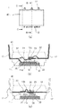
次に、屈曲予定領域Rbにおいて、枠15と共通リード13を折り曲げることにより、制御回路を給電方向の電力回路に向かってスライドさせる(ステップS40)。これにより、図2に示すように、制御素子23(ダイパッド12d)が、IGBT22の上方で、IGBT22(ダイパッド11d)にオーバーラップする。これにより、制御回路の少なくとも制御素子23を実装したダイパッド12d部分が、電力用半導体素子の上にオーバーラップした回路基板1P2ができあがる。そして、図4に示すように、ダイパッド11dの電力用半導体素子が接合された面の裏側の面(裏面)に絶縁被膜51を介してヒートシンク50を接続(ステップS50)し、電力用半導体装置の基本構成が形成される。
Next, in the planned bending region Rb, the control circuit is slid toward the power circuit in the feeding direction by bending the
このとき、パワー用ボンディングワイヤ31と制御用ボンディングワイヤ32は、それぞれ、電力回路内、制御回路内で位置が固定されているので、屈曲行程中(ステップS40)において、応力がかかることはない。さらに、信号用ボンディングワイヤ33も、それぞれ屈曲予定領域Rbを境に、IGBT22と共通リード13の電力回路側の部分との位置、制御素子23と共通リード13の制御回路側の部分との位置が固定されているので、屈曲行程中(ステップS40)において、応力がかかることはない。つまり、一枚のリードフレーム10を用いても、回路部材に余分な応力をかけることなく、電力用半導体素子21、22と制御素子23とが面内でオーバーラップするように階層化することができる。
At this time, since the positions of the
こうして形成した回路基板1P2をトランスファモールド用の金型内に設置する。そして、基本構成の封止領域Rs部分をトランスファモールドによって封止樹脂で封止する(ステップS60)。最後に封止体40からはみ出たリードフレーム10から枠体15を切除するとともに、タイバー16c、16pを切り離す。このようにして、バラバラになった外部端子(それぞれ11t、12t部分に対応)を所定の形状に折り曲げると(ステップS70)パワーリード11、制御リード11となり、電力用半導体装置1が完成する。
The circuit board 1P2 thus formed is placed in a transfer mold. Then, the sealing region Rs portion of the basic configuration is sealed with a sealing resin by a transfer mold (step S60). Finally, the
このとき、リードフレーム10の給電方向の両端に位置するタイバー16c、16pの近傍部分を含め上下の金型で挟まれる部分は、同一平面内に位置し、重なる部分もない。そのため、金型内での回路基板1P2の位置を容易に固定でき、樹脂の漏れの原因となる連通路を形成することもない。つまり、電力用半導体素子21、22と制御素子23とが面内でオーバーラップして階層化された回路基板1P2を、図4に示すように、封止樹脂40によって確実に封止できる電力用半導体装置1を得ることができる。
At this time, the portion sandwiched between the upper and lower molds including the vicinity of the tie bars 16c and 16p located at both ends of the
つぎに動作について説明する。
パワーリード11、制御リード12を外部回路に接続して電力用半導体装置1を起動させると、制御素子23からIGBT22に制御信号(ゲート信号)が出力され、IGBT22がONになる。すると、ダイオード21、IGBT22をはじめとする電力用半導体素子に電流が流れ、パワーリード11を介して、制御された主電力が出力される。その際、電気抵抗分の電力ロスが熱へと変換され、発熱が生ずるが、主な発熱源は電力用半導体素子21、22に偏るので、電力用半導体装置1内で温度差が生じる。しかも、半導体素子21、22、23とリードフレーム10、および封止樹脂40は、それぞれ線膨張係数が異なっているので、電力用半導体装置1内の部材間で、熱による変位に伴う応力(熱応力)が発生する。
Next, the operation will be described.
When the
しかし、本実施の形態にかかる電力用半導体装置1では、製造工程中に電気接続部に余計な応力が加わっていないので、接続部の耐久性が高い。さらに、回路基板1P2を正確に位置決めして、確実に封止しているので、回路内の部材が封止体40内で確実に保持され、湿気や有害なガスからも保護されるので、ますます信頼性が高くなる。
However, in the
つまり、従来のように、単に2枚のリードフレームで階層化しただけならば、回路内の部材の位置関係あるいは、封止にばらつきが生じて、信頼性が低下することがある。しかし、本実施の形態のように1枚のリードフレーム10の給電方向(リードパターン11i、11t、12i、12tの延在方向)の両端が一つの面内に収まるように、レベルを合わせて使用することで、確実に封止して、小型で信頼性の高い電力用半導体装置1を得ることができる。とくに、オーバーラップの際に折り曲げる屈曲予定領域Rbを挟んで電力回路側、制御回路側に分かれて配線部材33、32、33をボンディングするようにしたので、電気接合部の信頼性も高い。
In other words, as in the conventional case, if the layers are simply hierarchized by two lead frames, the positional relationship of the members in the circuit or the sealing may vary and reliability may be reduced. However, as in the present embodiment, the level is used so that both ends in the power feeding direction (the extending direction of the
実施の形態1の変形例.
また、図5に示すように、本変形例では、共通リード113として、上述した共通リード13から分岐した部分13eを制御回路側だけではなく、電力回路側にも形成するようにしてもよい。この場合、電力回路側の分岐部13eが、IGBT22のゲート電極の近傍にまで伸びるので、信号用ボンディングワイヤ33をより短くすることが可能となる。この場合でも、屈曲行程(ステップS40)中に、IGBT22と分岐部13eとの相対位置が保持されるので、応力がかかることはない。
Modification of the first embodiment.
Further, as shown in FIG. 5, in this modification, as the
なお、共通リード13や113には必ずしも分岐部13eを設ける必要はない。もちろん、分岐部13eが制御素子23やIGBT22に近づいていた分、信号用ボンディングワイヤ33を長くする必要が生じるが、上述したように。製造工程中に位置関係が変化しないので、工程中にダメージを受けることはない。
The common leads 13 and 113 are not necessarily provided with the
なお、本実施の形態および変形例においては、IGBT22のゲート電極と共通リード13とをワイヤボンディングで接合する例について説明したが、これに限ることはない。例えば、共通リード13を屈曲予定領域Rbよりも制御回路側の部分が、屈曲行程中(ステップS40)に電力回路側にスライドした時点で、ゲート電極に近接するように設計し、ゲート電極とゲート電極に近接した部分を、導電性接着剤などで電気的接続するようにしてもよい。
In the present embodiment and the modification, the example in which the gate electrode of the
また、本実施の形態および変形例においては、リードフレーム10、110の屈曲予定領域Rb部分も、通常の厚さのままプレス加工により、屈曲部13b、15bを形成したが、あらかじめ屈曲予定領域Rb部分をコイニング処理やハーフエッチングによって肉厚を薄くしておくことで曲げを容易にし、周辺部への歪を小さくすることが可能である。
In the present embodiment and modification, the bent portions Rb of the lead frames 10 and 110 are also formed into the
また、電力用半導体素子としてIGBT22とダイオード21の組み合わせを用い、図中の電力用半導体素子の数は合計4個で、並列接続であったが、これに限定するものではなく、いわゆる6 in 1やインテリジェントパワーモジュールにおいても同様の効果が得られる。
Further, a combination of
また、ダイボンド材料25としてSnAgCuはんだを用いたが、これに限定するものではなく、SnSbはんだや導電性接着剤などを用いても同様の効果が得られる。また、ワイヤボンド用の金属線として、所定の太さのAu線やAl線を用いたが、Cu線など他の金属や、リボンボンドなど他の形状の接合材料を用いても同様の効果が得られる。
In addition, although SnAgCu solder is used as the
また、本実施の形態1にかかる電力用半導体装置1の製造方法によれば、略矩形板状をなし、主電力を制御する電力用半導体素子21、22と電力用半導体素子21、22を制御する制御信号を出力する制御素子23とが厚み方向において段違いに配置されるとともに、矩形形状の両側面のそれぞれから並列する複数の端子11、12が突出配置された電力用半導体装置1を1枚のリードフレームを用いて製造する方法であって、1枚のリードフレーム10には、電力用半導体素子21、22が接合される第1のダイパッド11dと、制御素子23が接合される第2のダイパッド12dが、並列する複数の端子11、12となるリードパターン11i、11t、および12i、12tとともに、リードパターンの延在方向におけるそれぞれ一端側の領域と他端側の領域で連なるように形成されているとともに、一端側の領域から他端側の領域にかけて延在する延在パターンである共通リード13、枠体15が形成され、かつ、リードフレーム10の面に垂直な方向において第1のダイパッド11dに対して第2のダイパッド12dが上方に位置するように段差がつけられており、第1のダイパッド11dに電力用半導体素子21、22を接合するとともに、第2のダイパッド12dに制御素子23を接合する工程(ステップS20)と、リードフレーム10の面を保ったまま、屈曲予定領域Rbを屈曲させ、リードフレーム10の面に垂直な方向から見たときに、制御素子23を、電力用半導体素子21、22にオーバーラップさせる工程(ステップS40)と、第1のダイパッド11dの電力用半導体素子21、22が接合された面の反対側の面に、放熱部材50を接合する工程(ステップS50)と、リードフレーム10を少なくとも外枠15部分が露出した状態で図示しない上下の金型ではさみ、金型内に樹脂を流し込んで、放熱部材50の放熱面を除いて電力用半導体装置1を略矩形形状に封止する工程(ステップS60)と、を含むように構成した。
Further, according to the method for manufacturing the
そのため、配線部材33に応力をかけることがなく、屈曲部13bを形成できるので、回路基板1P2の信頼性が向上する。しかも、電力用半導体素子21、22と制御素子23が段違いに配置されているにもかかわらず、1枚のリードフレーム10を上下の金型でしっかりと挟み込むことができる。そのため、樹脂の漏れる隙間を生じさせることなく、リードフレーム10を金型内で固定して封止ができるので、封止信頼性も向上する。したがって、電力用半導体素子21、22の冷却に必要な面積を確保し、小型化できるとともに、封止体40を構成する封止樹脂を漏らすことなく回路基板1P2(リードフレーム10)を金型内で固定することにより、ばらつきなくしっかりと封止ができる。つまり、小型で、信頼性の高い電力用半導体装置1を得ることができる。
For this reason, since the
なお、換言すれば、本実施の形態1にかかる電力用半導体装置は、上記製造方法によって、略矩形板状をなし、主電力を制御する電力用半導体素子21、22と電力用半導体素子21、22を制御する制御信号を出力する制御素子23とが厚み方向において段違いに配置されるとともに、矩形板状の対向する側面のそれぞれから並列する複数の端子11、12が突出配置された電力用半導体装置1であって、一面に電力用半導体素子21、22が接合された第1のダイパッド11dと、第1のダイパッド11dの裏面に接合された放熱部材50と、電力用半導体素子21、22の上方に位置するとともに、制御素子23が接合された第2のダイパッド12dと、放熱部材50の放熱面を除いて当該電力用半導体装置1を略矩形形状に封止するように形成された封止体40と、を備え、少なくとも封止体40が形成されるまでは、第1のダイパッド11dと第2のダイパッド12dは、並列する複数の端子11、12となるリードパターン11i、11t、および12i、12tとともに、1枚のリードフレーム10、110(まとめて10)の面内で、リードパターン11i、11t、および12i、12tの延在方向におけるそれぞれ一端側の領域と他端側の領域で連なるように形成されているとともに、リードフレーム10内には、一端側の領域から他端側の領域にかけて延在する延在パターンとなる共通リード13、または枠体15が形成されており、リードフレーム10の面を保ったまま、延在パターンとなる枠体15または共通リード13の所定部分である屈曲予定領域Rbに屈曲部15bまたは13bを形成することにより、当該リードフレーム10の面に垂直な方向から見たときに、制御素子23が、電力用半導体素子21、22にオーバーラップするように構成したことになる。
In other words, the power semiconductor device according to the first embodiment is formed in a substantially rectangular plate shape by the above manufacturing method, and the
とくに、延在パターンとして形成した共通リード13における屈曲部13bまたは屈曲予定領域Rbよりも一端側の部分と電力用半導体素子22の制御電極とが配線部材33で電気接続されるとともに、共通リード13における屈曲部13bまたは屈曲予定領域Rbよりも他端側の部分と制御素子23の制御信号を出力する電極とが配線部材33で電気接続されているように構成したので、階層化するための屈曲行程中(ステップS40)において、配線部材33に応力がかかることがない。つまり、一枚のリードフレーム10を用いて、階層化するようにしても、配線部材33に余分な応力がかからないので、より一層信頼性の高い電力用半導体素子を得ることができる。
In particular, a portion of the
また、本実施の形態1にかかる電力用半導体装置1の製造方法では、延在パターン13の屈曲予定領域Rbまたは屈曲部13bよりも一端側の部分と電力用半導体素子22の制御電極とを配線部材33により電気接続するとともに、延在パターン13の屈曲予定領域Rbまたは屈曲部13bよりも他端側の部分と制御素子23の制御信号を出力する電極とを配線部材33により電気接続する工程(ステップS30)を有するようにしたので、特に、電力用半導体素子22と段差のある制御素子23間の電気接続部に応力がかからず、信頼性が向上する。
Further, in the method for manufacturing the
実施の形態2.
本実施の形態2にかかる電力用半導体装置では、実施の形態1にかかる電力用半導体装置で用いた共通リードに代えて、制御回路側と電力回路側に、それぞれ中継リードを設けて中継リード間をワイヤボンディングで接合したものである。さらに、制御回路を電力回路にオーバーラップする際のリードフレームの曲げ構造を変更したものである。図6は、本発明の実施の形態2にかかる電力用半導体装置を説明するためのもので、図6(a)は電力用半導体装置電を構成するためのリードフレームに半導体素子を接合し、配線部材を接続した状態の斜視図、図6(b)はリードフレームに半導体素子が実装され、さらに、オーバーラップのための曲げ加工を施したトランスファモールドによる封止工程直前状態の斜視図である。図において、実施の形態1における電力用半導体装置と同様の構成の部分には同じ符号を付し、詳細な説明は省略する。
Embodiment 2. FIG.
In the power semiconductor device according to the second embodiment, instead of the common leads used in the power semiconductor device according to the first embodiment, relay leads are provided on the control circuit side and the power circuit side, respectively, and between the relay leads. Are joined by wire bonding. Furthermore, the bending structure of the lead frame when the control circuit is overlapped with the power circuit is changed. FIG. 6 is a diagram for explaining a power semiconductor device according to a second embodiment of the present invention. FIG. 6A is a diagram illustrating a semiconductor element bonded to a lead frame for constituting a power semiconductor device. FIG. 6B is a perspective view of a state immediately before a sealing process by a transfer mold in which a semiconductor element is mounted on a lead frame and subjected to bending for overlapping. . In the figure, the same components as those in the power semiconductor device in the first embodiment are denoted by the same reference numerals, and detailed description thereof is omitted.
本実施の形態2にかかる電力用半導体装置の構成と製造方法について図に基づいて説明する。
電力用半導体装置の回路を構成するためのリードフレーム210は、1枚の銅板を打ち抜いて平面状のパターンを形成したもので、図6に示すように、枠体215の内側の領域のうち、屈曲予定領域Rbより図中右側の領域が制御回路を形成するためのパターン、屈曲予定領域Rbよりも左側の領域が電力回路を形成するためのパターンである。制御回路を形成するパターンには、給電方向において延在するように形成された複数のリードパターン12tと、複数のリードパターン12iとが、タイバー16cを介して連なるとともにそれぞれ並行に形成されている。電力回路を形成するパターンにも、給電方向において延在するように形成された複数のリードパターン11tと、複数のリードパターン11iとが、タイバー16pを介して連なるとともに、それぞれ並行に形成されている。
The configuration and manufacturing method of the power semiconductor device according to the second embodiment will be described with reference to the drawings.
A
これらも、実施の形態1と同様に、後の工程でタイバー16c、16p部分を切り離し、枠体215を除去することにより、一連の制御リード12と、パワーリード11として機能する。リードパターン12iのうち、ひとつのリードパターン12iの先端には、制御素子23である半導体の集積回路を接合するためのダイパッド12dが形成されている。そして、リードパターン11iのうち、ひとつのリードパターン11iの先端には、段差部11uを介して、ダイパッド11dが形成されている。
These also function as a series of control leads 12 and power leads 11 by cutting off the tie bars 16c and 16p and removing the
一方、本実施の形態2においては、枠体215の内側の領域のうち、並列方向における最外側に、電力回路側、制御回路側それぞれに、電力用半導体素子用中継リード14p、制御素子用中継リード14c(まとめて中継リード14と称する)が形成されている。このとき、中継リード14は、それぞれ少なくとも一部が、並列方向においてダイパッド11dおよびダイパッド11dよりも外側に位置するようにしている。また、枠体215の屈曲予定領域Rb部分には、開口部15hを中心として給電方向の両側に、それぞれ並列方向において向きが異なる切欠きとなる外側に開いた切欠き15noと内側に開いた切欠き15ni(まとめて切欠き部15と称する)が給電方向において距離を開けて形成されている。
On the other hand, in the second embodiment, the power semiconductor
つぎに、リードフレーム210に半導体素子を実装する方法について説明する。
なお、実施の形態1の図3で説明した工程のうち、ステップS10からS20まで、およびステップS50以降については、本実施の形態2においても同様であるので、説明を省略し、ステップS30〜S40に対応するステップS230〜S245(フローチャートとしては図示せず)について説明する。
Next, a method for mounting a semiconductor element on the
Of the steps described in FIG. 3 of the first embodiment, steps S10 to S20, and step S50 and subsequent steps are the same in the second embodiment, so the description thereof is omitted and steps S30 to S40 are omitted. Steps S230 to S245 (not shown in the flowchart) corresponding to the above will be described.
図6(a)に示すように、パワー用ボンディングワイヤ31を用いて、IGBT22(のエミッタ電極)とダイオード21とリードパターン11iとが連通するように、ワイヤボンディングにより電気的に接続する。そして、制御用ボンディングワイヤ32(Au線:太さ25μm)を用いて、制御素子23とリードパターン12iとをワイヤボンディングにより電気的に接続する。ここまでは、実施の形態1と同様である。そして、本実施の形態2においては、実施の形態1における信号用ボンディングワイヤ33と同様の信号用ボンディングワイヤ34(Au線:太さ25μm)を用いて、中継リード14pとIGBT22のゲート電極とをワイヤボンディングにより電気的に接続する(図中34pと表示)。さらに、信号用ボンディングワイヤ34を用いて、中継リード14cと、制御素子23の制御信号出力電極とをワイヤボンディングにより電気的に接続する(ステップS230)。これにより、屈曲予定領域Rbの右側には制御回路が、左側には電力スイッチを2組備えた電力回路が形成された回路基板201P1ができあがるが、この段階では制御素子23と、電力用半導体素子22間の給電経路が形成されていない。
As shown in FIG. 6A, the
このときも、実施の形態1と同様、ボンディングワイヤ31、32、34を用いてボンディングを行う際、リードフレーム210の面内でオーバーラップしている部材がないので、ボンディング部分より上に位置して作業の障害となる部材はなく、スムーズにボンディングすることができる。また、ボンディングワイヤ等の変形しやすい配線部材がボンディング部分の下側に位置することもなく、ボンディングによる超音波振動や加圧によりダメージを受けることもない。
At this time, as in the first embodiment, when bonding is performed using the
次に、図6(b)に示すように、リードフレーム210の枠体215の開口部15hに図示しない変形用ピンを差し込んみ、並列方向に引っ張り広げる。これにより、切欠き部15において枠体215は、リードフレーム210の面に平行な面内(水平方向)で折り曲げられて屈曲部215bとなり、制御回路が電力回路に向かってスライドし、制御素子23が電力用半導体素子21、22(ダイパッド11d)の上にオーバーラップする(ステップS240)。さらに、このスライドにより近接した中継リード14cと14p間をボンディングワイヤ34bを用いてワイヤボンドにて電気的に接合する(ステップS245)。これにより、制御素子23が、電力用半導体素子21、22(ダイパッド11d)上にオーバーラップした回路基板201P2ができあがる。あとは、実施の形態1で説明したステップS50の工程を行うことで、電力用半導体装置202の基本構成となる回路基板201P2が形成される。
Next, as shown in FIG. 6B, a deformation pin (not shown) is inserted into the
このとき、パワー用ボンディングワイヤ31と制御用ボンディングワイヤ32は、それぞれ、電力回路内、制御回路内で位置が固定されているので、屈曲行程中(ステップS40)において、応力がかかることはない。さらに、オーバーラップした後に行われる信号用ボンディングワイヤ34bの接合(ステップS245)は、並列方向において、ダイパッド11d、12dよりも外側に位置する部分で行われる。そのため、ボンディング位置が空間的に開放されているので、スムーズにボンディングすることができるとともに、ボンディングワイヤ等の変形しやすい配線部材がボンディング部分の下側に位置することもなく、ボンディングによる超音波振動や加圧によりダメージを受けることもない。つまり、一枚のリードフレーム210を用いても、回路部材に余分な応力をかけることなく、電力用半導体素子21、22と制御素子23とが面内でオーバーラップするように階層化することができる。
At this time, since the positions of the
また、本実施の形態2においても、リードフレーム210の給電方向の両端に位置するタイバー16c、16pの近傍部分を含め上下の金型で挟まれる部分は、同一平面内に位置し、重なる部分もない。そのため、金型内での回路基板201P2の位置を容易に固定でき、樹脂の漏れの原因となる連通路を形成することもない。つまり、電力用半導体素子21、22と制御素子23とが面内でオーバーラップして階層化された回路基板201P2を、確実に封止できる電力用半導体装置2を得ることができる。
Also in the second embodiment, the portions sandwiched between the upper and lower molds including the vicinity of the tie bars 16c and 16p located at both ends of the
なお、ここでは、中継リード14c、14pとをワイヤボンディングで接合する例について説明したが、これに限ることはない。例えば、制御回路側の部分が、屈曲行程中(ステップS240)に電力回路側にスライドした時点で、中継リード14cの一部が中継リード14pにオーバーラップするように設計し、オーバーラップ部分を、導電性接着剤やはんだ、または超音波圧接などで電気的接続を形成するようにしてもよい。
Although an example in which the relay leads 14c and 14p are joined by wire bonding has been described here, the present invention is not limited to this. For example, when the part on the control circuit side is slid to the power circuit side during the bending process (step S240), a part of the
また、本実施の形態においては、リードフレーム210の屈曲予定領域Rb部分も、通常の厚さのままプレス加工により、屈曲部215bを形成したが、あらかじめ屈曲予定領域Rb部分をコイニング処理やハーフエッチングによって肉厚を薄くしておくことで曲げを容易にし、周辺部への歪を小さくすることが可能である。
In the present embodiment, the
また、電力用半導体素子としてIGBT22とダイオード21の組み合わせを用い、図中の電力用半導体素子の数は合計4個で、並列接続であったが、これに限定するものではなく、いわゆる6 in 1やインテリジェントパワーモジュールにおいても同様の効果が得られる。また、ボンディングワイヤ34用の金属線として、所定の太さのAu線を用いたが、Al線やCu線など他の金属や、ボンディングリボン(テープ)など他の形状の接合材料を用いても同様の効果が得られる。
Further, a combination of
以上のように、本実施の形態2にかかる電力用半導体装置201によれば、略矩形板状をなし、略矩形板状をなし、主電力を制御する電力用半導体素子21、22と電力用半導体素子21、22を制御する制御信号を出力する制御素子23とが厚み方向において段違いに配置されるとともに、矩形板状の対向する側面のそれぞれから並列する複数の端子11、12が突出配置された電力用半導体装置201であって、一面に電力用半導体素子21、22が接合された第1のダイパッド11dと、第1のダイパッド11dの裏面に接合された放熱部材50と、電力用半導体素子21、22の上方に位置するとともに、制御素子23が接合された第2のダイパッド12dと、放熱部材50の放熱面を除いて当該電力用半導体装置201を略矩形形状に封止するように形成された封止体40と、を備え、少なくとも封止体40が形成されるまでは、第1のダイパッド11dと第2のダイパッド12dは、並列する複数の端子11、12となるリードパターン11i、11t、および12i、12tとともに、1枚のリードフレーム210の面内で、リードパターン11i、11t、および12i、12tの延在方向におけるそれぞれ一端側の領域と他端側の領域で連なるように形成されているとともに、リードフレーム210内には、一端側の領域から他端側の領域にかけて延在する延在パターンとなる枠体215が形成されており、リードフレーム210の面を保ったまま、延在パターンとなる枠体215の所定部分である屈曲予定領域Rbに屈曲部215bを形成することにより、当該リードフレーム210の面に垂直な方向から見たときに、制御素子23が、電力用半導体素子21、22にオーバーラップするように構成したことになる。
As described above, the power semiconductor device 201 according to the second embodiment has a substantially rectangular plate shape, a substantially rectangular plate shape, and the
そのため、電力用半導体素子21、22と制御素子23が段違いに配置されているにもかかわらず、リードフレーム210を上下の金型でしっかりと挟み込むことができる。そのため、電力用半導体素子21、22の冷却に必要な面積を確保し、小型化できるとともに、封止体40を構成する封止樹脂を漏らすことなく回路基板201P2(リードフレーム210)を金型内で固定することにより、ばらつきなくしっかりと封止ができる。つまり、小型で、信頼性の高い電力用半導体装置201を得ることができる。
Therefore, even though the
とくに、リードフレーム210の一端側の領域、および他端側の領域には、リードパターン11i、11t、および12i、12tが並列する方向において、それぞれ第1のダイパッド11dおよび第2のダイパッド12dよりも外側に位置する第1の中継リード14pと第2の中継リード14cが形成されており、第1の中継リード14pと電力用半導体素子22の制御電極、および、第2の中継リード14cと制御素子23の制御信号を出力する電極とが、それぞれ配線部材34p、34cで電気接続されているとともに、屈曲部215bの形成によって接近した第1の中継リード14pと第2の中継リード14cとが、配線部材34bで電気接続されているように構成したので、配線部材34p、34c、34bのボンディング位置が空間的に開放されているので、スムーズにボンディングすることができるとともに、ボンディングワイヤ等の変形しやすい配線部材がボンディング部分の下側に位置することもなく、ボンディングによる超音波振動や加圧によりダメージを受けることもない。つまり、一枚のリードフレーム210を用いても、回路部材に余分な応力をかけることなく、電力用半導体素子21、22と制御素子23とが面内でオーバーラップするように階層化することができる。
In particular, the
また、延在パターンである枠体215の屈曲予定領域Rbには、リードパターン11i、11t、および12i、12tが並列する方向において向きが異なる複数の切欠きが15no、15niが延在方向の異なる位置に設けられ、複数の切欠き15ni、15noを開くことにより、屈曲部215bをリードフレーム210の面に平行に形成するように構成したので、厚みを増大させることなく、1枚のリードフレーム210を用いて電力用半導体素子21、22と制御素子23を階層化させることができる。
In addition, in the planned bending region Rb of the
なお、延在パターンに切欠き15no、15niを設けて、面内方向に屈曲部215bを形成する構成は、上記実施の形態1や後述する実施の形態3など、他の実施の形態に応用することが可能である。
The configuration in which cutouts 15no and 15ni are provided in the extended pattern and the
実施の形態3.
本実施の形態3にかかる電力用半導体装置では、実施の形態1にかかる電力用半導体装置で用いた共通リードを設けることなく、制御素子と電力用半導体素子とを直接ボンディングワイヤで接合したものである。さらに、パワー用ボンディングワイヤではなく、内部リードの先端に設けたバス部を用いて、ダイオードとIGBTの出力電極を覆うように接合したものである。さらに、電力回路においてダイオードとIGBTの位置を逆に配置している。図7は、本発明の実施の形態3にかかる電力用半導体装置を説明するためのもので、図7(a)は電力用半導体装置を構成するためのリードフレームに半導体素子を接合し、配線部材を接続した状態の斜視図、図7(b)はリードフレームに半導体素子が実装され、さらに、オーバーラップのための曲げ加工を施したトランスファモールドによる封止工程直前状態の斜視図である。図において、実施の形態1における電力用半導体装置と同様の構成の部分には同じ符号を付し、詳細な説明は省略する。
Embodiment 3 FIG.
In the power semiconductor device according to the third embodiment, the control element and the power semiconductor device are directly bonded with a bonding wire without providing the common lead used in the power semiconductor device according to the first embodiment. is there. Furthermore, the diode is connected to cover the output electrode of the IGBT using a bus portion provided at the tip of the internal lead instead of the power bonding wire. Further, the positions of the diode and the IGBT are reversed in the power circuit. FIG. 7 is a diagram for explaining a power semiconductor device according to a third embodiment of the present invention. FIG. 7A is a diagram showing a wiring structure in which a semiconductor element is joined to a lead frame for constituting the power semiconductor device. FIG. 7B is a perspective view of a state immediately before a sealing process using a transfer mold in which a semiconductor element is mounted on a lead frame and subjected to bending processing for overlapping. In the figure, the same components as those in the power semiconductor device in the first embodiment are denoted by the same reference numerals, and detailed description thereof is omitted.
本実施の形態3にかかる電力用半導体装置の構成と製造方法について図に基づいて説明する。
電力用半導体装置の電力回路を構成するためのリードフレーム310は、1枚の銅板を打ち抜いて平面状のパターンを形成したもので、図7に示すように、枠体15の内側の領域のうち、屈曲予定領域Rbより図中右側の領域が制御回路を形成するためのパターン、屈曲予定領域Rbよりも左側の領域が電力回路を形成するためのパターンである。制御回路を形成するパターンには、給電方向において延在するように形成された複数のリードパターン12tと、複数のリードパターン12iとが、タイバー16cを介して連なるとともに、それぞれ並行に形成されている。電力回路を形成するパターンにも、給電方向において延在するように形成された複数のリードパターン11tと、複数のリードパターン11iとが、タイバー16pを介して連なるとともに、それぞれ並行に形成されている。
The configuration and manufacturing method of the power semiconductor device according to the third embodiment will be described with reference to the drawings.
A
これらも、実施の形態1と同様に、後の工程でタイバー16c、16p部分を切り離し、枠体15を除去することにより、一連の制御リード12と、パワーリード11として機能する。リードパターン12iのうち、ひとつのリードパターン12iの先端には、制御素子23である半導体の集積回路を接合するためのダイパッド12dが形成されている。そして、リードパターン11iのうち、ひとつのリードパターン11iの先端には、段差部11uを介して、ダイパッド11d形成されている。
These also function as a series of control leads 12 and power leads 11 by cutting off the tie bars 16c and 16p and removing the
一方、本実施の形態3においては、電力回路側の内部リードとなるリードパターン11iのうち、ダイパッド11dが形成されたリードパターン11iの並列方向における両外側には、リードパターン11iの延在方向において屈曲予定領域Rbを超えて制御回路のダイパッド12d部分にまで延在しているバスパターン311iが形成されており、さらに、バスパターン311iの制御回路側の端部には、並列方向においてダイパッド12dに一部がかかるバス部11jが形成されている。
On the other hand, in the third embodiment, out of the
つぎに、リードフレーム310に半導体素子を実装する方法について説明する。
なお、実施の形態1の図3で説明した工程のうち、ステップS50以降については、本実施の形態3においても同様であるので、説明を省略し、ステップS10〜ステップS40に対応するステップS310〜ステップS345(フローチャートとしては図示せず)について説明する。
Next, a method for mounting a semiconductor element on the
Of the steps described in FIG. 3 of the first embodiment, step S50 and the subsequent steps are the same in the third embodiment, and thus the description thereof is omitted, and steps S310 to S310 corresponding to steps S10 to S40 are omitted. Step S345 (not shown in the flowchart) will be described.
はじめに、平板状のリードフレーム310をプレス加工し、図7(a)に示すようにダイパッド11dが段差部11uにより、リードフレーム310平面より所定の段差分低くなるようにする。さらに、バス部11jがリードフレーム310平面より低く、かつ、ダイパッド11dの上面(表面)に対して、バス部11jの下面(裏面)の位置が、電力用半導体素子の厚みに接合部材の厚みを足した分高くなるように段差を付ける(図3:ステップS310)。
First, the
そして、段差加工したリードフレーム310に、IGBT22のゲート電極をタイバー16p側に向け、ダイオード21を内側になるように配置して、ステップS20と同様の手法ではあるが、半導体素子を実装する(ステップS340)。そして、制御用ボンディングワイヤ32(Au線:太さ25μm)を用いて、制御素子23とリードパターン12iとをワイヤボンディングにより電気的に接続する(ステップS330)。
Then, the semiconductor element is mounted in the same manner as in step S20 by placing the gate electrode of the
このときも、実施の形態1と同様、ボンディングワイヤ32を用いてボンディングを行う際、リードフレーム310の面内でオーバーラップしている部材がない。そのため、ボンディング部分より上に位置して作業の障害となる部材がなく、空間的に開放されているのでスムーズにボンディングすることができる。また、ボンディングワイヤ等の変形しやすい配線部材がボンディング部分の下側に位置することもなく、ボンディングによる超音波振動や加圧によりダメージを受けることもない。
At this time, as in the first embodiment, when bonding is performed using the
次に、枠体15、およびリードパターン311iの屈曲予定領域Rb部分を実施の形態1と同様の要領で屈曲加工する。これにより、制御回路が電力回路に向かってスライドし、ダイパッド12dがダイパッド11dに接合されたIGBT22の上にオーバーラップすると同時に、バス部11jの裏面が、ダイオード21とIGBT22の上方にまたがるように位置する(ステップS340)。なお、ダイオード21とIGBT22の表面には、屈曲工程(ステップS340)の前に導電性接着剤(例えば、焼結性Agペースト)が塗布(供給)されている。そのため、屈曲工程(ステップS340)後に、150℃で1hキュアすることによって、バス部11jがダイオード21とIGBT22を電気的に接続するとともに、リードパターン311iにも接続されることになる。さらに、スライドによって近づくとともに、リードフレーム310の面方向で並んだIGBT22のゲート電極と制御素子23とを信号用ボンディングワイヤ33と同様の信号用ボンディングワイヤ35(Au線:太さ25μm)を用いてボンディングにより電気的に接合する(ステップS345)。
Next, the
これにより、制御回路の少なくとも制御素子23を実装したダイパッド12d部分が、電力回路の上にオーバーラップした回路基板301P2ができあがる。あとは、実施の形態1で説明したステップS50の工程を行うことで、電力用半導体装置の基本構成が形成される。なお、バスパターン311jを折り曲げる工程は、枠体15に屈曲部15bを形成する工程とは別に行うようにしてもよい。
As a result, the circuit board 301P2 in which the
このとき、制御用ボンディングワイヤ32は、制御回路内で位置が固定されているので、屈曲行程中(ステップS340)において、応力がかかることはない。さらに、オーバーラップした後に行われる信号用ボンディングワイヤ35の接合(ステップS345)位置は空間的に開放されているので、スムーズにボンディングすることができるとともに、ボンディングワイヤ等の変形しやすい配線部材がボンディング部分の下側に位置することもなく、ボンディングによる超音波振動や加圧によりダメージを受けることもない。つまり、一枚のリードフレームを用いても、回路部材に余分な応力をかけることなく、電力用半導体素子21、22と制御素子23とが面内でオーバーラップするように階層化することができる。
At this time, since the position of the
このとき、リードフレーム310の給電方向の両端に位置するタイバー16c、16pの近傍部分を含め上下の金型で挟まれる部分は、同一平面内に位置し、重なる部分もない。そのため、金型内での基本構成の位置を容易に固定でき、樹脂の漏れの原因となる連通口を形成することもない。つまり、電力用半導体素子21、22と制御素子23とが面内でオーバーラップして階層化された回路基板301P2を、確実に封止できる電力用半導体装置301を得ることができる。
At this time, the portion sandwiched between the upper and lower molds including the vicinity of the tie bars 16c and 16p located at both ends of the
なお、ここでは、リードフレーム310の屈曲予定領域Rb部分も、通常の厚さのままプレス加工により、屈曲部15b、11bを形成したが、あらかじめ屈曲予定領域Rb部分をコイニング処理やハーフエッチングによって肉厚を薄くしておくことで曲げを容易にし、周辺部への歪を小さくすることが可能である。
In this case, the
また、バス部11jはプレス加工(ステップS310)により基準面よりやや低くなるように段差付けしており、バス部11jの裏面が電力用半導体素子であるIGBT22、ダイオード21の表面の高さにほぼ等しくなるように形成されているが、厚み調整ができる接合材料で接続できる場合にはこれにこだわる必要はない。さらに、バス部11jと電力用半導体素子21、22との電気的接続に導電性接着剤を用いたが、はんだ接合や超音波圧接など、他の方法を用いても同様の効果が得られる。
Further, the
また、IGBT22のゲート電極と制御素子23に信号用ボンディングワイヤ35をボンディングする場合、ダイパッド11dに図示しない開口部を形成し、開口部からピンを突き上げて、制御素子23のダイパッド12dを保持するようにしてもよい。それにより、よりワイヤボンドを容易にすることが可能となる。また、制御素子23用のダイパッド12dを廃し、バス部11jの上に絶縁性ダイボンドシート接着剤などを用いて制御素子23を搭載するようにすれば、さらなる小型化が可能となる。
Further, when the
また、電力用半導体素子としてIGBT22とダイオード21の組み合わせを用い、図中の電力用半導体素子の数は合計4個で、並列接続であったが、これに限定するものではなく、いわゆる6 in 1やインテリジェントパワーモジュールにおいても同様の効果が得られる。また、ボンディングワイヤ35用の金属線として、所定の太さのAu線を用いたが、Al線やCu線など他の金属や、リボンボンドなど他の形状の接合材料を用いても同様の効果が得られる。
Further, a combination of
以上のように、本実施の形態3にかかる電力用半導体装置301によれば、略矩形板状をなし、略矩形板状をなし、主電力を制御する電力用半導体素子21、22と電力用半導体素子21、22を制御する制御信号を出力する制御素子23とが厚み方向において段違いに配置されるとともに、矩形板状の対向する側面のそれぞれから並列する複数の端子11、12が突出配置された電力用半導体装置301であって、一面に電力用半導体素子21、22が接合された第1のダイパッド11dと、第1のダイパッド11dの裏面に接合された放熱部材50と、電力用半導体素子21、22の上方に位置するとともに、制御素子23が接合された第2のダイパッド12dと、放熱部材50の放熱面を除いて当該電力用半導体装置301を略矩形形状に封止するように形成された封止体40と、を備え、少なくとも封止体40が形成されるまでは、第1のダイパッド11dと第2のダイパッド12dは、並列する複数の端子11、12となるリードパターン11i、11t、および12i、12tとともに、1枚のリードフレーム310の面内で、リードパターン11i、11t、および12i、12tの延在方向におけるそれぞれ一端側の領域と他端側の領域で連なるように形成されているとともに、リードフレーム310内には、一端側の領域から他端側の領域にかけて延在する延在パターンとなる枠体15が形成されており、リードフレーム310の面を保ったまま、延在パターンとなる枠体15所定部分である屈曲予定領域Rbに屈曲部15bを形成することにより、当該リードフレーム310の面に垂直な方向から見たときに、制御素子23が、電力用半導体素子21、22にオーバーラップするように構成したことになる。
As described above, the power semiconductor device 301 according to the third embodiment has a substantially rectangular plate shape, a substantially rectangular plate shape, and the
そのため、電力用半導体素子21、22と制御素子23が段違いに配置されているにもかかわらず、リードフレーム310を上下の金型でしっかりと挟み込むことができる。そのため、電力用半導体素子21、22の冷却に必要な面積を確保し、小型化できるとともに、封止体40を構成する封止樹脂を漏らすことなく回路基板301P2(リードフレーム310)を金型内で固定することにより、ばらつきなくしっかりと封止ができる。つまり、小型で、信頼性の高い電力用半導体装置301を得ることができる。
Therefore, even though the
とくに、電力用半導体素子は、整流素子21とスイッチング素子22からなる2つの半導体素子を並べたものであり、リードフレーム310には、一端側の領域から他端側の領域に達するとともに、他端側の端部に所定の大きさのバス部11jを有するバスパターン311iが形成されており、バスパターン311iのバス部11j以外の部分の折り曲げによって、バス部11jを2つの半導体素子21、22にオーバーラップさせて、2つの半導体素子21、22間が電気接続されているとともに、屈曲部15bの形成によって接近した電力用半導体素子22の制御電極と制御素子23の制御信号を出力する電極とが配線部材35で電気接続されているように構成した。そのため、オーバーラップした後に行われる信号用ボンディングワイヤ35の接合位置は空間的に開放されているので、スムーズにボンディングすることができるとともに、ボンディングワイヤ等の変形しやすい配線部材がボンディング部分の下側に位置することもなく、ボンディングによる超音波振動や加圧によりダメージを受けることもない。つまり、一枚のリードフレーム310を用いても、回路部材に余分な応力をかけることなく、信頼性の高い電力用半導体装置301を得ることができる。
In particular, the power semiconductor element is formed by arranging two semiconductor elements including the rectifying
以上のように上記各実施の形態1〜3にかかる電力用半導体装置の製造方法によれば、略矩形板状をなし、主電力を制御する電力用半導体素子21、22と電力用半導体素子21、22を制御する制御信号を出力する制御素子23とが厚み方向において段違いに配置されるとともに、矩形形状の両側面のそれぞれから並列する複数の端子11、12が突出配置された電力用半導体装置1、201、301(代表して1)を1枚のリードフレーム10、210、310(代表して10)を用いて製造する方法であって、1枚のリードフレーム10には、電力用半導体素子21、22が接合される第1のダイパッド11dと、制御素子23が接合される第2のダイパッド12dが、並列する複数の端子11、12となるリードパターン11i、11t、および12i、12tとともに、リードパターンの延在方向におけるそれぞれ一端側の領域と他端側の領域で連なるように形成されているとともに、一端側の領域から他端側の領域にかけて延在する延在パターンである共通リード13、枠体15が形成され、かつ、リードフレーム10の面に垂直な方向において第1のダイパッド11dに対して第2のダイパッド12dが上方に位置するように段差がつけられており、第1のダイパッド11dに電力用半導体素子21、22を接合するとともに、第2のダイパッド12dに制御素子23を接合する工程(ステップS20)と、リードフレーム10の面を保ったまま、屈曲予定領域Rbを屈曲させ、リードフレーム10の面に垂直な方向から見たときに、制御素子23を、電力用半導体素子21、22にオーバーラップさせる工程(ステップS40)と、第1のダイパッド11dの電力用半導体素子21、22が接合された面の反対側の面に、放熱部材50を接合する工程(ステップS50)と、リードフレーム10を少なくとも外枠15部分が露出した状態で図示しない上下の金型ではさみ、金型内に樹脂を流し込んで、放熱部材50の放熱面を除いて電力用半導体装置1を略矩形形状に封止する工程(ステップS60)と、を含むように構成した。
As described above, according to the method for manufacturing the power semiconductor device according to each of the first to third embodiments, the
そのため、配線部材33に応力をかけることがなく、屈曲部13bを形成できるので、回路基板1P2の信頼性が向上する。しかも、電力用半導体素子21、22と制御素子23が段違いに配置されているにもかかわらず、1枚のリードフレーム10を上下の金型でしっかりと挟み込むことができる。そのため、樹脂の漏れる隙間を生じさせることなく、リードフレーム10を金型内で固定して封止ができるので、封止信頼性も向上する。したがって、電力用半導体素子21、22の冷却に必要な面積を確保し、小型化できるとともに、封止体40を構成する封止樹脂を漏らすことなく回路基板1P2(リードフレーム10)を金型内で固定することにより、ばらつきなくしっかりと封止ができる。つまり、小型で、信頼性の高い電力用半導体装置1を得ることができる。
For this reason, since the
上記各実施の形態において、ダイパッド11dをリードフレーム10、210、310の主面より低くする例について説明したが、これに限ることはない。例えば、ダイパッド12dを主面より高くするようにしてもよく、11dを低くするとともに、12dを高くするようにしてもよい。つまり、ダイパッド11dが12dより所定量低くなるようにすればよい。そして、ダイパッド11d、12dやバス部11jを段差加工工程(ステップS10、S310)で段差付けする例について記載したが、リードフレームを打ち抜く時に同時に行うようにしてもよい。
In each of the above embodiments, the example in which the
なお、上記各実施の形態においては、スイッチング素子(トランジスタ)22や整流素子(ダイオード)21として機能する電力用半導体素子には、シリコンウエハを基材とした一般的な素子でも良いが、本発明においては炭化ケイ素(SiC)や窒化ガリウム(GaN)、またはダイヤモンドといったシリコンと較べてバンドギャップが広い、いわゆるワイドバンドギャップ半導体材料を用い、運転温度が高くなる場合に、特に顕著な効果が現れる。特に炭化ケイ素を用いた電力用半導体素子に好適に用いることができる。デバイス種類としては、スイッチング素子としてはIGBTの他に、MOSFET(Metal Oxide Semiconductor Field-Effect-Transistor)でもよい。 In each of the above-described embodiments, the power semiconductor element functioning as the switching element (transistor) 22 or the rectifying element (diode) 21 may be a general element based on a silicon wafer. In particular, a so-called wide band gap semiconductor material having a wider band gap than silicon such as silicon carbide (SiC), gallium nitride (GaN), or diamond is used, and a particularly remarkable effect appears when the operating temperature is increased. In particular, it can be suitably used for a power semiconductor element using silicon carbide. As the device type, the switching element may be a MOSFET (Metal Oxide Semiconductor Field-Effect-Transistor) in addition to the IGBT.
ワイドバンドギャップ半導体によって形成されたスイッチング素子や整流素子(各実施の形態における電力用半導体素子21、22)は、ケイ素で形成された素子よりも電力損失が低いため、スイッチング素子や整流素子における高効率化が可能であり、ひいては、電力用半導体装置の高効率化が可能となる。さらに、耐電圧性が高く、許容電流密度も高いため、スイッチング素子や整流素子の小型化が可能であり、これら小型化されたスイッチング素子や整流素子を用いることにより、電力用半導体装置も小型化が可能となる。また耐熱性が高いので、高温動作が可能であり、ヒートシンクの放熱フィンの小型化や、水冷部の空冷化も可能となるので、電力用半導体装置の一層の小型化が可能になる。
Since switching elements and rectifier elements (
一方、上記のように高温動作する場合は停止・駆動時の温度差が大きくなり、さらに、高効率・小型化によって、単位体積当たりに扱う電流量が大きくなる。そのため経時的な温度変化や空間的な温度勾配が大きくなり、電力用半導体素子と配線部材との熱応力も大きくなる可能性がある。しかし、本発明のように製造中の電気接続部の応力を防止し、リードフレームによって正確な位置で固定して、確実に封止することができる電力用半導体装置では、接合部の信頼性が高く、部材の劣化も抑制できるので、ワイドバンドギャップ半導体の特性を活かして、小型化や高効率化を進めてもパワーサイクル寿命が長く、信頼性の高い電力用半導体装置を得ることが容易となる。つまり、本発明による効果を発揮することで、ワイドバンドギャップ半導体の特性を活かすことができるようになる。 On the other hand, when operating at a high temperature as described above, the temperature difference during stop and drive increases, and the amount of current handled per unit volume increases due to high efficiency and downsizing. Therefore, the temperature change over time and the spatial temperature gradient increase, and the thermal stress between the power semiconductor element and the wiring member may increase. However, in the power semiconductor device that can prevent the stress of the electrical connection part during manufacture and fix it in an accurate position by the lead frame and securely seal it as in the present invention, the reliability of the joint part is high. It is easy to obtain a highly reliable power semiconductor device with a long power cycle life even if miniaturization and high efficiency are promoted by taking advantage of the characteristics of wide band gap semiconductors. Become. That is, by exhibiting the effect of the present invention, the characteristics of the wide band gap semiconductor can be utilized.
なお、スイッチング素子及び整流素子の両方がワイドバンドギャップ半導体によって形成されていても、いずれか一方の素子がワイドバンドギャップ半導体によって形成されていてもよい。 Note that both the switching element and the rectifying element may be formed of a wide band gap semiconductor, or one of the elements may be formed of a wide band gap semiconductor.
1 電力用半導体装置、
10 リードフレーム;
11 パワーリード(端子)、
11d:ダイパッド、11i:内部リード対応リードパターン、11j:バス部、11t:外部端子対応リードパターン、11u:段差部対応リードパターン)、
12 制御リード(端子)、
12d:ダイパッド、12i:内部リード対応リードパターン、12t:外部端子対応リードパターン)
13 共通リード(延在パターン(13b:屈曲部、13e:分岐部))、
14 中継リード(14c:制御回路対応部分、14p:電力回路対応部分)
15 枠体(延在パターン(15b:屈曲部、15h:開口部、15ni:内開き切欠き部、15no:外開き切欠き部))、
16 タイバー(16c:制御回路対応部分、16p:電力回路対応部分)
21 ダイオード(整流素子:電力用半導体素子)、 22 IGBT(スイッチング素子:電力用半導体素子)、 23 制御素子、 25 ダイボンド材料、
31 パワー用ボンディングワイヤ(配線部材)、 32 制御用ボンディングワイヤ(配線部材)、 33 信号用ボンディングワイヤ(配線部材)、
40 封止体、 50 放熱板、 51 絶縁層
Rb:リードフレームの屈曲予定領域、 Rs 封止予定領域、
百位の数字の違いは変形例または実施の形態による構成の相違を示す。
1 Power semiconductor devices,
10 lead frame;
11 Power lead (terminal),
11d: die pad, 11i: lead pattern corresponding to internal lead, 11j: bus portion, 11t: lead pattern corresponding to external terminal, 11u: lead pattern corresponding to stepped portion),
12 Control lead (terminal),
12d: die pad, 12i: lead pattern corresponding to internal leads, 12t: lead pattern corresponding to external terminals)
13 common leads (extended pattern (13b: bent portion, 13e: branched portion)),
14 Relay lead (14c: Control circuit corresponding part, 14p: Power circuit corresponding part)
15 frame (extended pattern (15b: bent portion, 15h: opening, 15ni: inner opening notch, 15no: outer opening notch)),
16 tie bars (16c: control circuit corresponding part, 16p: power circuit corresponding part)
21 diode (rectifier element: power semiconductor element), 22 IGBT (switching element: power semiconductor element), 23 control element, 25 die bond material,
31 bonding wire for power (wiring member), 32 bonding wire for control (wiring member), 33 bonding wire for signal (wiring member),
40 sealing body, 50 heat sink, 51 insulating layer Rb: lead frame bending planned area, Rs sealing planned area,
The difference in the hundreds indicates a difference in configuration according to the modification or the embodiment.
Claims (6)
前記一枚のリードフレームには、前記電力用半導体素子が接合される第1のダイパッドと、前記制御素子が接合される第2のダイパッドが、前記並列する複数の端子となるリードパターンとともに、前記リードパターンの延在方向におけるそれぞれ一端側の領域と他端側の領域で連なるように形成されているとともに、前記一端側の領域から前記他端側の領域にかけて延在する延在パターンが形成され、かつ、前記リードフレームの面に垂直な方向において前記第1のダイパッドに対して前記第2のダイパッドが上方に位置するように段差がつけられており、
前記第1のダイパッドの一面に前記電力用半導体素子を接合するとともに、前記第2のダイパッドに前記制御素子を接合する工程と、
前記リードフレームの面を保ったまま、前記延在パターンの所定部分を屈曲させ、前記リードフレームの面に垂直な方向から見たときに、前記制御素子を、前記電力用半導体素子にオーバーラップさせる工程と、
前記第1のダイパッドの裏面に、放熱部材を接合する工程と、
前記リードフレームを少なくとも外枠部分が露出した状態で上下の金型ではさみ、前記金型内に樹脂を流し込んで、前記放熱部材の放熱面を除いて当該電力用半導体装置を矩形形状に封止する工程と、
を含む電力用半導体装置の製造方法により製造した電力用半導体装置において、
前記延在パターンにおける前記所定部分よりも前記一端側の部分と前記電力用半導体素子の制御電極とが配線部材で電気接続されるとともに、前記延在パターンにおける前記所定部分よりも前記他端側の部分と前記制御素子の制御信号を出力する電極とが配線部材で電気接続されていることを特徴とする電力用半導体装置。 A rectangular power semiconductor element for controlling main power and a control element for outputting a control signal for controlling the power semiconductor element are arranged in a stepwise manner in the thickness direction, and are opposed to the rectangular plate shape. A method of manufacturing a power semiconductor device in which a plurality of terminals juxtaposed from each of the side surfaces is arranged using a single lead frame,
The one lead frame includes a first die pad to which the power semiconductor element is bonded and a second die pad to which the control element is bonded together with a lead pattern serving as the plurality of terminals arranged in parallel. A lead pattern is formed so as to be continuous in one end side region and the other end side region in the extending direction of the lead pattern, and an extension pattern extending from the one end side region to the other end side region is formed. And a step is provided so that the second die pad is positioned above the first die pad in a direction perpendicular to the surface of the lead frame.
Bonding the power semiconductor element to one surface of the first die pad and bonding the control element to the second die pad;
A predetermined portion of the extended pattern is bent while maintaining the surface of the lead frame, and the control element is overlapped with the power semiconductor element when viewed from a direction perpendicular to the surface of the lead frame. Process,
Bonding a heat dissipating member to the back surface of the first die pad;
The lead frame is sandwiched between upper and lower molds with at least the outer frame portion exposed, and resin is poured into the mold to seal the power semiconductor device in a rectangular shape except for the heat radiation surface of the heat radiation member And a process of
In a power semiconductor device manufactured by a method for manufacturing a power semiconductor device including:
A portion on the one end side of the predetermined pattern in the extended pattern and the control electrode of the power semiconductor element are electrically connected by a wiring member, and the other end side of the predetermined portion in the extended pattern is on the other end side. A power semiconductor device, wherein the portion and an electrode for outputting a control signal of the control element are electrically connected by a wiring member .
前記一枚のリードフレームには、前記電力用半導体素子が接合される第1のダイパッドと、前記制御素子が接合される第2のダイパッドが、前記並列する複数の端子となるリードパターンとともに、前記リードパターンの延在方向におけるそれぞれ一端側の領域と他端側の領域で連なるように形成されているとともに、前記一端側の領域から前記他端側の領域にかけて延在する延在パターンが形成され、かつ、前記リードフレームの面に垂直な方向において前記第1のダイパッドに対して前記第2のダイパッドが上方に位置するように段差がつけられており、
前記第1のダイパッドの一面に前記電力用半導体素子を接合するとともに、前記第2のダイパッドに前記制御素子を接合する工程と、
前記リードフレームの面を保ったまま、前記延在パターンの所定部分を屈曲させ、前記リードフレームの面に垂直な方向から見たときに、前記制御素子を、前記電力用半導体素子にオーバーラップさせる工程と、
前記第1のダイパッドの裏面に、放熱部材を接合する工程と、
前記リードフレームを少なくとも外枠部分が露出した状態で上下の金型ではさみ、前記金型内に樹脂を流し込んで、前記放熱部材の放熱面を除いて当該電力用半導体装置を矩形形状に封止する工程と、
を含む電力用半導体装置の製造方法により製造した電力用半導体装置において、
前記リードフレームの前記一端側の領域、および前記他端側の領域には、前記リードパターンが並列する方向において、それぞれ前記第1のダイパッドおよび前記第2のダイパッドよりも外側に位置する第1の中継リードと第2の中継リードが形成されており、 前記第1の中継リードと前記電力用半導体素子の制御電極、および、前記第2の中継リードと前記制御素子の制御信号を出力する電極とが、それぞれ配線部材で電気接続されているとともに、
前記屈曲によって接近した前記第1の中継リードと前記第2の中継リードとが、配線部材で電気接続されていることを特徴とする電力用半導体装置。 A rectangular power semiconductor element for controlling main power and a control element for outputting a control signal for controlling the power semiconductor element are arranged in a stepwise manner in the thickness direction, and are opposed to the rectangular plate shape. A method of manufacturing a power semiconductor device in which a plurality of terminals juxtaposed from each of the side surfaces is arranged using a single lead frame,
The one lead frame includes a first die pad to which the power semiconductor element is bonded and a second die pad to which the control element is bonded together with a lead pattern serving as the plurality of terminals arranged in parallel. A lead pattern is formed so as to be continuous in one end side region and the other end side region in the extending direction of the lead pattern, and an extension pattern extending from the one end side region to the other end side region is formed. And a step is provided so that the second die pad is positioned above the first die pad in a direction perpendicular to the surface of the lead frame.
Bonding the power semiconductor element to one surface of the first die pad and bonding the control element to the second die pad;
A predetermined portion of the extended pattern is bent while maintaining the surface of the lead frame, and the control element is overlapped with the power semiconductor element when viewed from a direction perpendicular to the surface of the lead frame. Process,
Bonding a heat dissipating member to the back surface of the first die pad;
The lead frame is sandwiched between upper and lower molds with at least the outer frame portion exposed, and resin is poured into the mold to seal the power semiconductor device in a rectangular shape except for the heat radiation surface of the heat radiation member And a process of
In a power semiconductor device manufactured by a method for manufacturing a power semiconductor device including:
In the region on the one end side and the region on the other end side of the lead frame, the first die pad located outside the first die pad and the second die pad in the direction in which the lead patterns are arranged in parallel, respectively. A relay lead and a second relay lead are formed, the first relay lead and the control electrode of the power semiconductor element, and the second relay lead and an electrode for outputting a control signal of the control element; Are electrically connected with each wiring member,
The power semiconductor device, wherein the first relay lead and the second relay lead that are approached by the bending are electrically connected by a wiring member .
前記一枚のリードフレームには、前記電力用半導体素子が接合される第1のダイパッドと、前記制御素子が接合される第2のダイパッドが、前記並列する複数の端子となるリードパターンとともに、前記リードパターンの延在方向におけるそれぞれ一端側の領域と他端側の領域で連なるように形成されているとともに、前記一端側の領域から前記他端側の領域にかけて延在する延在パターンが形成され、かつ、前記リードフレームの面に垂直な方向において前記第1のダイパッドに対して前記第2のダイパッドが上方に位置するように段差がつけられており、
前記第1のダイパッドの一面に前記電力用半導体素子を接合するとともに、前記第2のダイパッドに前記制御素子を接合する工程と、
前記リードフレームの面を保ったまま、前記延在パターンの所定部分を屈曲させ、前記リードフレームの面に垂直な方向から見たときに、前記制御素子を、前記電力用半導体素子にオーバーラップさせる工程と、
前記第1のダイパッドの裏面に、放熱部材を接合する工程と、
前記リードフレームを少なくとも外枠部分が露出した状態で上下の金型ではさみ、前記金型内に樹脂を流し込んで、前記放熱部材の放熱面を除いて当該電力用半導体装置を矩形形状に封止する工程と、
を含む電力用半導体装置の製造方法により製造した電力用半導体装置において、
前記電力用半導体素子は、整流素子とスイッチング素子からなる2つの半導体素子を並列配置したものであり、
前記リードフレームには、前記一端側の領域から前記他端側の領域に達するとともに、前記他端側の端部に所定の大きさのバス部を有するバスパターンが形成されており、
前記バスパターンの前記バス部以外の部分の折り曲げによって、前記バス部を前記2つの半導体素子にオーバーラップさせて、前記2つの半導体素子間が電気接続されているとともに、
前記屈曲によって接近した前記電力用半導体素子の制御電極と前記制御素子の制御信号を出力する電極とが配線部材で電気接続されていることを特徴とする電力用半導体装置。 A rectangular power semiconductor element for controlling main power and a control element for outputting a control signal for controlling the power semiconductor element are arranged in a stepwise manner in the thickness direction, and are opposed to the rectangular plate shape. A method of manufacturing a power semiconductor device in which a plurality of terminals juxtaposed from each of the side surfaces is arranged using a single lead frame,
The one lead frame includes a first die pad to which the power semiconductor element is bonded and a second die pad to which the control element is bonded together with a lead pattern serving as the plurality of terminals arranged in parallel. A lead pattern is formed so as to be continuous in one end side region and the other end side region in the extending direction of the lead pattern, and an extension pattern extending from the one end side region to the other end side region is formed. And a step is provided so that the second die pad is positioned above the first die pad in a direction perpendicular to the surface of the lead frame.
Bonding the power semiconductor element to one surface of the first die pad and bonding the control element to the second die pad;
A predetermined portion of the extended pattern is bent while maintaining the surface of the lead frame, and the control element is overlapped with the power semiconductor element when viewed from a direction perpendicular to the surface of the lead frame. Process,
Bonding a heat dissipating member to the back surface of the first die pad;
The lead frame is sandwiched between upper and lower molds with at least the outer frame portion exposed, and resin is poured into the mold to seal the power semiconductor device in a rectangular shape except for the heat radiation surface of the heat radiation member And a process of
In a power semiconductor device manufactured by a method for manufacturing a power semiconductor device including:
The power semiconductor element is a parallel arrangement of two semiconductor elements consisting of a rectifying element and a switching element,
The lead frame is formed with a bus pattern having a predetermined size bus portion at the other end side from the one end side region to the other end side region,
By bending the portion other than the bus portion of the bus pattern, the bus portion overlaps the two semiconductor elements, and the two semiconductor elements are electrically connected,
A power semiconductor device, wherein a control electrode of the power semiconductor element approached by the bending and an electrode outputting a control signal of the control element are electrically connected by a wiring member .
前記一枚のリードフレームには、前記電力用半導体素子が接合される第1のダイパッドと、前記制御素子が接合される第2のダイパッドが、前記並列する複数の端子となるリードパターンとともに、前記リードパターンの延在方向におけるそれぞれ一端側の領域と他端側の領域で連なるように形成されているとともに、前記一端側の領域から前記他端側の領域にかけて延在する延在パターンが形成され、かつ、前記リードフレームの面に垂直な方向において前記第1のダイパッドに対して前記第2のダイパッドが上方に位置するように段差がつけられており、
前記第1のダイパッドの一面に前記電力用半導体素子を接合するとともに、前記第2のダイパッドに前記制御素子を接合する工程と、
前記リードフレームの面を保ったまま、前記延在パターンの所定部分を屈曲させ、前記リードフレームの面に垂直な方向から見たときに、前記制御素子を、前記電力用半導体素子にオーバーラップさせる工程と、
前記第1のダイパッドの裏面に、放熱部材を接合する工程と、
前記リードフレームを少なくとも外枠部分が露出した状態で上下の金型ではさみ、前記金型内に樹脂を流し込んで、前記放熱部材の放熱面を除いて当該電力用半導体装置を矩形形状に封止する工程と、
を含む電力用半導体装置の製造方法により製造した電力用半導体装置において、
前記延在パターンの所定部分には、前記リードパターンが並列する方向において向きが異なる複数の切欠きが前記延在方向の異なる位置に設けられ、
前記複数の切欠きを開くことにより、前記所定部分が前記リードパターンの面に平行な方向で屈曲していることを特徴とする電力用半導体装置。 A rectangular power semiconductor element for controlling main power and a control element for outputting a control signal for controlling the power semiconductor element are arranged in a stepwise manner in the thickness direction, and are opposed to the rectangular plate shape. A method of manufacturing a power semiconductor device in which a plurality of terminals juxtaposed from each of the side surfaces is arranged using a single lead frame,
The one lead frame includes a first die pad to which the power semiconductor element is bonded and a second die pad to which the control element is bonded together with a lead pattern serving as the plurality of terminals arranged in parallel. A lead pattern is formed so as to be continuous in one end side region and the other end side region in the extending direction of the lead pattern, and an extension pattern extending from the one end side region to the other end side region is formed. And a step is provided so that the second die pad is positioned above the first die pad in a direction perpendicular to the surface of the lead frame.
Bonding the power semiconductor element to one surface of the first die pad and bonding the control element to the second die pad;
A predetermined portion of the extended pattern is bent while maintaining the surface of the lead frame, and the control element is overlapped with the power semiconductor element when viewed from a direction perpendicular to the surface of the lead frame. Process,
Bonding a heat dissipating member to the back surface of the first die pad;
The lead frame is sandwiched between upper and lower molds with at least the outer frame portion exposed, and resin is poured into the mold to seal the power semiconductor device in a rectangular shape except for the heat radiation surface of the heat radiation member And a process of
In a power semiconductor device manufactured by a method for manufacturing a power semiconductor device including:
In the predetermined portion of the extending pattern, a plurality of notches having different directions in the direction in which the lead patterns are arranged in parallel are provided at different positions in the extending direction,
The power semiconductor device, wherein the predetermined portion is bent in a direction parallel to the surface of the lead pattern by opening the plurality of notches .
Priority Applications (1)
| Application Number | Priority Date | Filing Date | Title |
|---|---|---|---|
| JP2011236784A JP5676413B2 (en) | 2011-10-28 | 2011-10-28 | Power semiconductor device |
Applications Claiming Priority (1)
| Application Number | Priority Date | Filing Date | Title |
|---|---|---|---|
| JP2011236784A JP5676413B2 (en) | 2011-10-28 | 2011-10-28 | Power semiconductor device |
Publications (3)
| Publication Number | Publication Date |
|---|---|
| JP2013098199A JP2013098199A (en) | 2013-05-20 |
| JP2013098199A5 JP2013098199A5 (en) | 2014-01-09 |
| JP5676413B2 true JP5676413B2 (en) | 2015-02-25 |
Family
ID=48619888
Family Applications (1)
| Application Number | Title | Priority Date | Filing Date |
|---|---|---|---|
| JP2011236784A Active JP5676413B2 (en) | 2011-10-28 | 2011-10-28 | Power semiconductor device |
Country Status (1)
| Country | Link |
|---|---|
| JP (1) | JP5676413B2 (en) |
Cited By (1)
| Publication number | Priority date | Publication date | Assignee | Title |
|---|---|---|---|---|
| US9376514B2 (en) | 2012-09-20 | 2016-06-28 | Lg Chem, Ltd. | Vinyl chloride latex with low energy consumption and method for preparing the same |
Families Citing this family (2)
| Publication number | Priority date | Publication date | Assignee | Title |
|---|---|---|---|---|
| WO2015178296A1 (en) | 2014-05-20 | 2015-11-26 | 三菱電機株式会社 | Semiconductor device for electric power |
| DE112020006890T5 (en) * | 2020-03-13 | 2022-12-22 | Mitsubishi Electric Corporation | SEMICONDUCTOR DEVICE AND POWER CONVERTER |
Family Cites Families (8)
| Publication number | Priority date | Publication date | Assignee | Title |
|---|---|---|---|---|
| JPS55149957U (en) * | 1979-04-13 | 1980-10-29 | ||
| JPS57170560U (en) * | 1981-04-21 | 1982-10-27 | ||
| JPS62219649A (en) * | 1986-03-20 | 1987-09-26 | Hitachi Ltd | Electronic device |
| JPH06140558A (en) * | 1992-10-29 | 1994-05-20 | Sanyo Electric Co Ltd | Semiconductor device |
| JP3067560B2 (en) * | 1994-12-02 | 2000-07-17 | 松下電器産業株式会社 | Electronic component manufacturing method |
| JP2004022601A (en) * | 2002-06-12 | 2004-01-22 | Mitsubishi Electric Corp | Semiconductor device |
| JP2006080300A (en) * | 2004-09-09 | 2006-03-23 | Kokusan Denki Co Ltd | Lead frame and its manufacturing method |
| JP2011066289A (en) * | 2009-09-18 | 2011-03-31 | Renesas Electronics Corp | Method of manufacturing semiconductor device |
-
2011
- 2011-10-28 JP JP2011236784A patent/JP5676413B2/en active Active
Cited By (1)
| Publication number | Priority date | Publication date | Assignee | Title |
|---|---|---|---|---|
| US9376514B2 (en) | 2012-09-20 | 2016-06-28 | Lg Chem, Ltd. | Vinyl chloride latex with low energy consumption and method for preparing the same |
Also Published As
| Publication number | Publication date |
|---|---|
| JP2013098199A (en) | 2013-05-20 |
Similar Documents
| Publication | Publication Date | Title |
|---|---|---|
| JP6234630B2 (en) | Power module | |
| JP5279632B2 (en) | Semiconductor module | |
| TWI450373B (en) | Dual side cooling integrated power device package and module and methods of manufacture | |
| US9673118B2 (en) | Power module and method of manufacturing power module | |
| JP5272191B2 (en) | Semiconductor device and manufacturing method of semiconductor device | |
| US8188583B2 (en) | Semiconductor device and method of manufacturing same | |
| JP5863602B2 (en) | Power semiconductor device | |
| CN108735692B (en) | Semiconductor device with a semiconductor device having a plurality of semiconductor chips | |
| JP6114149B2 (en) | Semiconductor device | |
| JP2007184501A (en) | Resin-sealed semiconductor device with externally exposed radiators at its top, and method for fabrication thereof | |
| JP5676413B2 (en) | Power semiconductor device | |
| JP5233853B2 (en) | Semiconductor device | |
| JP2015115471A (en) | Power semiconductor device | |
| US11398447B2 (en) | Semiconductor device and method for producing semiconductor device | |
| JP2018116960A (en) | Power semiconductor device | |
| JP2022143167A (en) | Semiconductor device | |
| CN111354709A (en) | Semiconductor device and method for manufacturing the same | |
| JP2021077817A (en) | Semiconductor device | |
| JP2021027146A (en) | Semiconductor device | |
| JP2019079891A (en) | Semiconductor device | |
| WO2021200138A1 (en) | Semiconductor device | |
| JP5741526B2 (en) | Semiconductor device and manufacturing method thereof | |
| JP7118204B1 (en) | semiconductor equipment | |
| JP2013187268A (en) | Semiconductor module | |
| WO2021220357A1 (en) | Semiconductor device |
Legal Events
| Date | Code | Title | Description |
|---|---|---|---|
| A521 | Request for written amendment filed |
Free format text: JAPANESE INTERMEDIATE CODE: A523 Effective date: 20131114 |
|
| A621 | Written request for application examination |
Free format text: JAPANESE INTERMEDIATE CODE: A621 Effective date: 20131114 |
|
| A977 | Report on retrieval |
Free format text: JAPANESE INTERMEDIATE CODE: A971007 Effective date: 20140530 |
|
| A131 | Notification of reasons for refusal |
Free format text: JAPANESE INTERMEDIATE CODE: A131 Effective date: 20140916 |
|
| A521 | Request for written amendment filed |
Free format text: JAPANESE INTERMEDIATE CODE: A523 Effective date: 20141031 |
|
| TRDD | Decision of grant or rejection written | ||
| A01 | Written decision to grant a patent or to grant a registration (utility model) |
Free format text: JAPANESE INTERMEDIATE CODE: A01 Effective date: 20141202 |
|
| A61 | First payment of annual fees (during grant procedure) |
Free format text: JAPANESE INTERMEDIATE CODE: A61 Effective date: 20141225 |
|
| R151 | Written notification of patent or utility model registration |
Ref document number: 5676413 Country of ref document: JP Free format text: JAPANESE INTERMEDIATE CODE: R151 |
|
| R250 | Receipt of annual fees |
Free format text: JAPANESE INTERMEDIATE CODE: R250 |
|
| R250 | Receipt of annual fees |
Free format text: JAPANESE INTERMEDIATE CODE: R250 |
|
| R250 | Receipt of annual fees |
Free format text: JAPANESE INTERMEDIATE CODE: R250 |
|
| R250 | Receipt of annual fees |
Free format text: JAPANESE INTERMEDIATE CODE: R250 |
|
| R250 | Receipt of annual fees |
Free format text: JAPANESE INTERMEDIATE CODE: R250 |
|
| R250 | Receipt of annual fees |
Free format text: JAPANESE INTERMEDIATE CODE: R250 |
|
| R250 | Receipt of annual fees |
Free format text: JAPANESE INTERMEDIATE CODE: R250 |