JP5662701B2 - Clock supply device - Google Patents
Clock supply device Download PDFInfo
- Publication number
- JP5662701B2 JP5662701B2 JP2010120371A JP2010120371A JP5662701B2 JP 5662701 B2 JP5662701 B2 JP 5662701B2 JP 2010120371 A JP2010120371 A JP 2010120371A JP 2010120371 A JP2010120371 A JP 2010120371A JP 5662701 B2 JP5662701 B2 JP 5662701B2
- Authority
- JP
- Japan
- Prior art keywords
- clock
- signal
- reset
- flip
- control signal
- Prior art date
- Legal status (The legal status is an assumption and is not a legal conclusion. Google has not performed a legal analysis and makes no representation as to the accuracy of the status listed.)
- Active
Links
- 230000007274 generation of a signal involved in cell-cell signaling Effects 0.000 claims description 76
- 230000004913 activation Effects 0.000 claims 1
- 238000010586 diagram Methods 0.000 description 58
- 230000002093 peripheral effect Effects 0.000 description 40
- 238000000034 method Methods 0.000 description 17
- 238000004519 manufacturing process Methods 0.000 description 11
- 230000001360 synchronised effect Effects 0.000 description 11
- 230000000630 rising effect Effects 0.000 description 10
- 230000003111 delayed effect Effects 0.000 description 4
- 238000012986 modification Methods 0.000 description 2
- 230000004048 modification Effects 0.000 description 2
- 230000010355 oscillation Effects 0.000 description 2
- 230000000644 propagated effect Effects 0.000 description 1
- 239000004065 semiconductor Substances 0.000 description 1
- 230000003068 static effect Effects 0.000 description 1
Images


Classifications
-
- H—ELECTRICITY
- H03—ELECTRONIC CIRCUITRY
- H03L—AUTOMATIC CONTROL, STARTING, SYNCHRONISATION OR STABILISATION OF GENERATORS OF ELECTRONIC OSCILLATIONS OR PULSES
- H03L7/00—Automatic control of frequency or phase; Synchronisation
-
- G—PHYSICS
- G06—COMPUTING; CALCULATING OR COUNTING
- G06F—ELECTRIC DIGITAL DATA PROCESSING
- G06F1/00—Details not covered by groups G06F3/00 - G06F13/00 and G06F21/00
- G06F1/04—Generating or distributing clock signals or signals derived directly therefrom
- G06F1/06—Clock generators producing several clock signals
-
- G—PHYSICS
- G06—COMPUTING; CALCULATING OR COUNTING
- G06F—ELECTRIC DIGITAL DATA PROCESSING
- G06F1/00—Details not covered by groups G06F3/00 - G06F13/00 and G06F21/00
- G06F1/26—Power supply means, e.g. regulation thereof
- G06F1/32—Means for saving power
- G06F1/3203—Power management, i.e. event-based initiation of a power-saving mode
- G06F1/3234—Power saving characterised by the action undertaken
- G06F1/324—Power saving characterised by the action undertaken by lowering clock frequency
-
- G—PHYSICS
- G06—COMPUTING; CALCULATING OR COUNTING
- G06F—ELECTRIC DIGITAL DATA PROCESSING
- G06F1/00—Details not covered by groups G06F3/00 - G06F13/00 and G06F21/00
- G06F1/24—Resetting means
-
- Y—GENERAL TAGGING OF NEW TECHNOLOGICAL DEVELOPMENTS; GENERAL TAGGING OF CROSS-SECTIONAL TECHNOLOGIES SPANNING OVER SEVERAL SECTIONS OF THE IPC; TECHNICAL SUBJECTS COVERED BY FORMER USPC CROSS-REFERENCE ART COLLECTIONS [XRACs] AND DIGESTS
- Y02—TECHNOLOGIES OR APPLICATIONS FOR MITIGATION OR ADAPTATION AGAINST CLIMATE CHANGE
- Y02D—CLIMATE CHANGE MITIGATION TECHNOLOGIES IN INFORMATION AND COMMUNICATION TECHNOLOGIES [ICT], I.E. INFORMATION AND COMMUNICATION TECHNOLOGIES AIMING AT THE REDUCTION OF THEIR OWN ENERGY USE
- Y02D10/00—Energy efficient computing, e.g. low power processors, power management or thermal management
-
- Y—GENERAL TAGGING OF NEW TECHNOLOGICAL DEVELOPMENTS; GENERAL TAGGING OF CROSS-SECTIONAL TECHNOLOGIES SPANNING OVER SEVERAL SECTIONS OF THE IPC; TECHNICAL SUBJECTS COVERED BY FORMER USPC CROSS-REFERENCE ART COLLECTIONS [XRACs] AND DIGESTS
- Y02—TECHNOLOGIES OR APPLICATIONS FOR MITIGATION OR ADAPTATION AGAINST CLIMATE CHANGE
- Y02D—CLIMATE CHANGE MITIGATION TECHNOLOGIES IN INFORMATION AND COMMUNICATION TECHNOLOGIES [ICT], I.E. INFORMATION AND COMMUNICATION TECHNOLOGIES AIMING AT THE REDUCTION OF THEIR OWN ENERGY USE
- Y02D30/00—Reducing energy consumption in communication networks
- Y02D30/50—Reducing energy consumption in communication networks in wire-line communication networks, e.g. low power modes or reduced link rate
Landscapes
- Engineering & Computer Science (AREA)
- Theoretical Computer Science (AREA)
- Physics & Mathematics (AREA)
- General Engineering & Computer Science (AREA)
- General Physics & Mathematics (AREA)
- Logic Circuits (AREA)
Description
本発明は、回路ブロックにクロック信号を供給するクロック供給装置に関するものである。 The present invention relates to a clock supply device that supplies a clock signal to a circuit block.
半導体集積回路装置(以下、LSI)及びLSIを実装するシステムの電源と熱の設計・製造は、LSI及びシステムの最大の消費電力に合わせる必要がある。また、LSIの電源設計・製造は、LSIの最大の消費電流にも合わせる必要がある。消費電力や消費電流が大きいと、設計・製造の難易度と価格のコストが高くなるため、LSIの消費電力及び消費電流を削減する技術が提案されている。 The power supply and heat design and manufacture of a semiconductor integrated circuit device (hereinafter referred to as LSI) and a system on which the LSI is mounted must be matched to the maximum power consumption of the LSI and the system. In addition, the power supply design / manufacturing of the LSI needs to match the maximum current consumption of the LSI. When the power consumption and current consumption are large, the difficulty of design and manufacturing and the cost of the price increase. Therefore, a technique for reducing the power consumption and current consumption of the LSI has been proposed.
ここで、クロック信号に同期して動作する論理回路からなるLSIの消費電力は、リーク電流等による静的なものを除くと、クロック同期動作による動的な動作に起因するものである。動的な消費電力は、クロック信号に同期して状態を変化させるフリップフロップの動作を基準にして考えることができる。 Here, the power consumption of an LSI composed of a logic circuit that operates in synchronization with a clock signal is due to a dynamic operation by a clock synchronization operation, excluding static ones due to a leakage current or the like. Dynamic power consumption can be considered based on the operation of a flip-flop that changes state in synchronization with a clock signal.
フリップフロップの動作において動的に電力を消費するのは、フリップフロップを動作させる入力クロック信号のアクティブエッジが入力される時の次の2つの動作である。1つは、入力データを内部に保持するラッチ動作であり、もう1つは、ラッチ動作時に出力するデータを変化させるトグル動作である。なお、ラッチ動作で消費する電力というのは、フリップフロップそのもので消費する電力の他に、入力クロック信号を伝達するためのバッファ等の電力も含まれるものとする。また、トグル動作で消費する電力というのは、フリップフロップそのもので消費する電力の他に、出力データ信号を伝達するためのバッファ等の電力も含まれるものとする。 The power consumption dynamically in the operation of the flip-flop is the following two operations when the active edge of the input clock signal that operates the flip-flop is input. One is a latch operation that holds input data therein, and the other is a toggle operation that changes data output during the latch operation. Note that the power consumed by the latch operation includes power of a buffer for transmitting the input clock signal in addition to the power consumed by the flip-flop itself. In addition, the power consumed by the toggle operation includes power such as a buffer for transmitting an output data signal in addition to power consumed by the flip-flop itself.
以上のような背景の下、論理回路の消費電力及び消費電流を削減する技術として、回路中のフリップフロップのイネーブル制御が非アクティブの期間はそのフリップフロップを駆動するクロックを止めるという、イネーブルによるクロックゲーティング技術がある。この技術は、論理的に不要なラッチ動作を行わないように制御して消費電力を削減する技術である。各フリップフロップが必要な時だけラッチ動作を行い、入力クロック信号のアクティブエッジ入力に応じて常に全てのフリップフロップがラッチ動作しないため、消費電流も削減することが可能である。 Under the background described above, as a technique for reducing the power consumption and current consumption of the logic circuit, the clock for enabling the flip-flop is stopped during the period when the enable control of the flip-flop in the circuit is inactive. There is gating technology. This technique is a technique for reducing power consumption by controlling not to perform a logically unnecessary latch operation. The latch operation is performed only when each flip-flop is necessary, and all the flip-flops are not always latched in accordance with the input of the active edge of the input clock signal, so that the current consumption can be reduced.
また、論理回路のリセット動作時の消費電力を削減する技術として、リセット動作時に通常動作時よりもクロック周波数を低くする技術がある(特許文献1)。この技術は、充分長いリセット期間の間のラッチ動作の回数を必要最小限にまで削減することで総消費電力及び単位時間あたりの消費電力を削減する技術である。 As a technique for reducing the power consumption during the reset operation of the logic circuit, there is a technique for lowering the clock frequency during the reset operation than during the normal operation (Patent Document 1). This technique reduces the total power consumption and the power consumption per unit time by reducing the number of latch operations during a sufficiently long reset period to the minimum necessary.
また、論理回路のリセット動作時の消費電流を削減する技術として、リセット動作時に複数の回路ブロックに対し独立なクロックを供給制御して各回路ブロックのリセット期間を重複させない技術がある(特許文献2)。この技術は、リセット期間中に全ての回路ブロックに同時にクロックを供給しないように制御することで1クロックサイクルあたりの瞬間的な消費電流を削減する技術である。 In addition, as a technique for reducing current consumption during a reset operation of a logic circuit, there is a technique for controlling the supply of independent clocks to a plurality of circuit blocks during a reset operation so that the reset periods of the circuit blocks do not overlap (Patent Document 2). ). This technique is a technique for reducing instantaneous current consumption per clock cycle by controlling not to supply clocks to all circuit blocks simultaneously during the reset period.
しかしながら、リセット動作時にはフリップフロップのイネーブル制御は論理的に常にアクティブとなるため、前述のイネーブルによるクロックゲーティング技術ではクロックを止めることができずに消費電力及び消費電流を削減することができない。そのため、論理回路の内容によっては通常動作時よりもリセット動作時の方が消費電力や消費電流が高くなるものもある。その場合は、通常動作時の消費電力や消費電流が低くできても、電源と熱の設計・製造は、通常動作時の消費電力と消費電流ではなくてリセット動作時の最大消費電力と最大消費電流に合わせる必要がある。 However, since the flip-flop enable control is logically always active during the reset operation, the clock gating technique based on enable cannot stop the clock and cannot reduce power consumption and current consumption. For this reason, depending on the contents of the logic circuit, power consumption and current consumption may be higher during the reset operation than during the normal operation. In that case, even if the power consumption and current consumption during normal operation can be reduced, the design and manufacture of the power supply and heat is not the power consumption and current consumption during normal operation, but the maximum power consumption and maximum consumption during reset operation. It is necessary to match the current.
また、リセット動作時に通常動作時よりもクロック周波数を低くする技術では、リセット期間中のラッチ動作の総回数が減るので結果として消費電力を削減することが可能であるが、1クロックあたりにラッチ動作するフリップフロップ数は減らせない。つまり、アクティブなクロックエッジの入力に対して全てのフリップフロップが動作するのは変わらないので、1クロックあたりの瞬間的な消費電流を削減することはできない。そのため、論理回路の内容によっては通常動作時よりもリセット動作時の方が消費電流が高くなるものもある。その場合は、前述のイネーブルによるクロックゲーティング技術で通常動作時の消費電流が低くできても、電源の設計・製造はその通常動作時の消費電流ではなくてリセット動作時の最大消費電流に合わせる必要がある。 In addition, the technique of lowering the clock frequency during the reset operation than during the normal operation reduces the total number of latch operations during the reset period, and as a result, can reduce power consumption. The number of flip-flops to be performed cannot be reduced. In other words, since all flip-flops operate in response to an active clock edge input, the instantaneous current consumption per clock cannot be reduced. For this reason, depending on the contents of the logic circuit, the current consumption may be higher during the reset operation than during the normal operation. In such a case, even if the current consumption during normal operation can be reduced by the clock gating technology using the above-mentioned enable, the power supply design / manufacturing should match the maximum current consumption during reset operation, not the current consumption during normal operation. There is a need.
またさらに、リセット動作時に複数の回路ブロックに独立なクロックを供給制御して各回路ブロックのリセット期間を重複させない技術は、各回路ブロックそれぞれのリセット期間が全て重ならないように制御することで消費電流を削減することができる。しかし、各回路ブロックに論理的な接続がある場合、リセット期間が全て重ならないことにより完全なリセットができない可能性がある。それは以下の仕組みによる。 Furthermore, the technology that does not overlap the reset period of each circuit block by supplying independent clocks to a plurality of circuit blocks during the reset operation is controlled by controlling the reset periods of each circuit block so that they do not overlap. Can be reduced. However, when there is a logical connection in each circuit block, there is a possibility that a complete reset cannot be performed because the reset periods do not all overlap. It is based on the following mechanism.
リセット端子のないフリップフロップは、リセット信号がアクティブな間は入力データがL又はHどちらか一方に固定されるように論理回路を組むことでクロック同期のリセットを行うことができる。ただ、論理回路の設計上、リセット信号がアクティブな間にも入力データがL又はHどちらか一方に固定されないフリップフロップが含まれることがある。そのようなフリップフロップは入力データピンに論理的に接続された全てのフリップフロップをリセットした後、アクティブなクロックエッジを入力して初めてリセットすることが可能である。したがって、フリップフロップの入力データピンに論理的に接続されたフリップフロップの中に、まだリセットされていない別の回路ブロックのフリップフロップが含まれる場合は、このフリップフロップをリセットすることができない。つまり、複数の回路ブロックに含まれるフリップフロップが相互に接続されている場合に、全ての回路ブロックのリセット期間を独立にすると完全なリセットができなくなるおそれがある。 A flip-flop without a reset terminal can perform clock-synchronized reset by assembling a logic circuit so that input data is fixed to either L or H while the reset signal is active. However, a logic circuit design may include a flip-flop in which input data is not fixed to either L or H while the reset signal is active. Such a flip-flop can be reset only after an active clock edge is input after all flip-flops logically connected to the input data pins have been reset. Therefore, when the flip-flop logically connected to the input data pin of the flip-flop includes a flip-flop of another circuit block that has not been reset yet, the flip-flop cannot be reset. That is, when flip-flops included in a plurality of circuit blocks are connected to each other, if the reset periods of all the circuit blocks are made independent, there is a possibility that complete reset cannot be performed.
本発明は、上記の問題点を解決するためになされたものである。本発明の目的は、複数の回路ブロック全体のピーク消費電流を軽減しつつ、複数の回路ブロック全体のリセットを適切に行える仕組を提供することである。 The present invention has been made to solve the above problems. An object of the present invention is to provide a mechanism that can appropriately reset the entire plurality of circuit blocks while reducing the peak current consumption of the entire plurality of circuit blocks.
本発明は、第1の回路ブロックおよび第2の回路ブロックに対してクロック信号を供給するクロック供給装置であって、第1制御信号および第2制御信号のそれぞれを供給する第1制御信号生成手段および第2制御信号生成手段と、前記第1制御信号生成手段から供給される前記第1制御信号および前記第2制御信号のうちの前記第1制御信号が入力され、前記第1制御信号を用いて、前記第1の回路ブロックをリセットするためのクロック信号であって所定の期間アクティブとなる第1クロック信号を前記第1の回路ブロックに供給する第1クロック制御手段と、前記第2制御信号生成手段から供給される前記第1制御信号および前記第2制御信号のうちの前記第2制御信号が入力され、前記第2制御信号を用いて、前記第2の回路ブロックをリセットするためのクロック信号であって前記所定の期間とは異なる期間アクティブとなる第2クロック信号を前記第2の回路ブロックに供給する第2クロック制御手段と、を有することを特徴とする。 The present invention is a clock supply device for supplying a clock signal to a first circuit block and a second circuit block, and a first control signal generating means for supplying a first control signal and a second control signal, respectively. And the second control signal generating means, and the first control signal of the first control signal and the second control signal supplied from the first control signal generating means is input, and the first control signal is used. Te, a first clock control means for supplying a first clock signal which is a predetermined period of time active to said first circuit block to a clock signal for resetting the first circuit block, the second control signal the second control signal of said first control signal and the second control signal is supplied from the generating means is input, using the second control signal, said second circuit block And having a second clock control means for supplying a second clock signal comprising different active during the second circuit block and the predetermined period of time a clock signal to reset the.
本発明によれば、複数の回路ブロック全体のピーク消費電流を軽減しつつ、複数の回路ブロック全体のリセットを適切に行えるようにできる。 According to the present invention, it is possible to appropriately reset the entire plurality of circuit blocks while reducing the peak current consumption of the entire plurality of circuit blocks.
以下、本発明のクロック供給装置の一実施形態について図面を用いて説明する。 Hereinafter, an embodiment of a clock supply device of the present invention will be described with reference to the drawings.
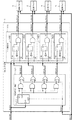
図1は、本発明の実施例1に係るクロック供給装置の外部接続構成、及び、内部構成を示すブロック図である。
図1において、1はクロック供給装置である。2は回路ブロックA、3は回路ブロックB、4は回路ブロックC、5は回路ブロックDである。クロック供給装置1は、回路ブロックA2、回路ブロックB3、回路ブロックC4、及び、回路ブロックD5に対してクロック供給を行う。
FIG. 1 is a block diagram illustrating an external connection configuration and an internal configuration of a clock supply device according to a first embodiment of the present invention.
In FIG. 1,
クロック供給装置1において、101は制御信号生成部、102はクロック制御部である。1011は2ビットカウンタである。1021、1022、1023、及び、1024はクロックゲーティングセルである。
In the
クロック供給装置1は、図示しないクロック発振装置、図示しないリセット生成装置、回路ブロックA2、回路ブロックB3、回路ブロックC4、及び、回路ブロックD5と接続されている。クロック供給装置1は、図示しないクロック発振装置が出力するクロック信号CLOCKに同期して動作する。クロック供給装置1は、図示しないリセット生成装置が出力するリセット信号RESETをクロック信号に同期して受信し、リセット信号がLレベルの間は通常動作期間、また、リセット信号がHレベルの間はリセット期間であると認識して動作する。クロック供給装置1は、回路ブロックA2に対してクロック信号CLOCK_A、回路ブロックB3に対してクロック信号CLOCK_B、回路ブロックC4に対してクロック信号CLOCK_C、回路ブロックD5に対してクロック信号CLOCK_Dを出力する。
The
回路ブロックA2、B3、C4、及び、D5は、クロック供給装置1、及び、図示しないリセット生成装置と接続されている。回路ブロックA2は、クロック供給装置1が出力するクロック信号CLOCK_Aに同期して動作する。回路ブロックB3は、クロック供給装置1が出力するクロック信号CLOCK_Bに同期して動作する。回路ブロックC4は、クロック供給装置1が出力するクロック信号CLOCK_Cに同期して動作する。回路ブロックはD5は、クロック供給装置1が出力するクロック信号CLOCK_Dに同期して動作する。
The circuit blocks A2, B3, C4, and D5 are connected to the
回路ブロックA2、B3、C4、及び、D5は、図示しないリセット生成装置が出力するリセット信号RESETを受信し、リセット信号がLレベルの間は通常動作を行い、また、Hレベルの間はリセット動作、すなわち内部のフリップフロップの初期化を行う。 The circuit blocks A2, B3, C4, and D5 receive a reset signal RESET output from a reset generator (not shown), perform normal operation while the reset signal is at L level, and perform reset operation when the reset signal is at H level. That is, the internal flip-flop is initialized.
制御信号生成部101は、クロック信号CLOCKの信号線、リセット信号RESETの信号線、及び、クロック制御部102と接続されており、クロック信号に同期して動作する。制御信号生成部101は、リセット信号を受信し、リセット信号がLレベルの間は通常動作期間、また、リセット信号がHレベルの間はリセット期間であると認識して動作する。制御信号生成部101は、クロック制御部102に対して複数の制御信号ENABLE_A、ENABLE_B、ENABLE_C、及び、ENABLE_Dを送信する。
The control
クロック制御部102は、クロック信号CLOCKの信号線、制御信号生成部101、出力クロック信号CLOCK_A、CLOCK_B、CLOCK_C、及び、CLOCK_Dの各信号線と接続されている。クロック制御部102は、クロック信号を使用して動作する。クロック制御部102は、制御信号生成部101から出力される複数の制御信号ENABLE_A、ENABLE_B、ENABLE_C、及び、ENABLE_Dを受信する。クロック制御部102は、複数の制御信号ENABLE_A、ENABLE_B、ENABLE_C、及び、ENABLE_Dに応じて、出力クロック信号CLOCK_A、CLOCK_B、CLOCK_C、及び、CLOCK_Dを出力する。
The
2ビットカウンタ1011は、クロック信号CLOCK、リセット信号RESET、及び、組み合わせ回路を介して出力信号ENABLE_A、ENABLE_B、ENABLE_C、及び、ENABLE_Dの各信号線と接続されている。2ビットカウンタ1011は、カウント動作についてはクロック信号に同期して、また、初期化動作についてはクロック信号に非同期で動作する。
The 2-
2ビットカウンタ1011は、リセット信号を受信し、リセット信号RESETがLレベルの間はカウンタ出力値Q[1:0]を「0」に初期化する。また、2ビットカウンタ1011は、リセット信号RESETがHレベルの間(リセット動作時)はクロック信号に同期してカウント動作を行い、カウンタ出力Q[1:0]を毎クロック1ずつ増加させる。2ビットカウンタ1011は、2ビットのカウンタ出力値Q[1:0]を持ち、通常動作時のカウンタ出力値Q[1:0]は、「0」、「1」、「2」、「3」の繰り返しとなる。なおここでは、カウンタ出力値は、H/Lレベルではなく、Hを「1」として、Lを「0」として解釈した2進数を10進数表記に変えて表現している。
The 2-
出力信号ENABLE_Aは、リセット信号がLレベルのときか、又は、カウンタ出力値Q[1:0]の値が「0」のときにHレベル、それ以外のときにLレベルとなる。出力信号ENABLE_Bは、リセット信号がLレベルのときか、又は、カウンタ出力値Q[1:0]の値が「1」のときにHレベル、それ以外のときにLレベルとなる。出力信号ENABLE_Cは、リセット信号がLレベルのときか、又は、カウンタ出力値Q[1:0]の値が「2」のときにHレベル、それ以外のときにLレベルとなる。出力信号ENABLE_Dは、リセット信号がLレベルのときか、又は、カウンタ出力値Q[1:0]の値が「3」のときにHレベル、それ以外のときにLレベルとなる。即ち、制御信号生成部101は、リセット動作時、カウンタ1011が示す異なるカウント値(0、1、2、3)に対応する期間(異なる期間)にアクティブとなる複数の制御信号(ENABLE_A〜D)を生成する。
The output signal ENABLE_A is H level when the reset signal is L level or the counter output value Q [1: 0] is “0”, and is L level otherwise. The output signal ENABLE_B is H level when the reset signal is L level or the counter output value Q [1: 0] is “1”, and is L level otherwise. The output signal ENABLE_C is H level when the reset signal is L level or the counter output value Q [1: 0] is “2”, and is L level otherwise. The output signal ENABLE_D is H level when the reset signal is L level or the counter output value Q [1: 0] is “3”, and is L level otherwise. That is, the control
クロックゲーティングセル1021は、クロック信号CLOCK、入力信号ENABLE_A、及び出力クロック信号CLOCK_Aの各信号線とそれぞれCI、ENB、及びCO端子と接続されており、クロック信号に含まれるクロックパルスを間引く動作を行う。クロックゲーティングセル1022は、クロック信号CLOCK、入力信号ENABLE_B、及び出力クロック信号CLOCK_Bの各信号線とそれぞれCI、ENB、及びCO端子と接続されており、クロック信号に含まれるクロックパルスを間引く動作を行う。クロックゲーティングセル1023は、クロック信号CLOCK、入力信号ENABLE_C、及び出力クロック信号CLOCK_Cの各信号線とそれぞれCI、ENB、及びCO端子と接続されており、クロック信号に含まれるクロックパルスを間引く動作を行う。クロックゲーティングセル1024は、クロック信号CLOCK、入力信号ENABLE_D、及び出力クロック信号CLOCK_Dの各信号線とそれぞれCI、ENB、及びCO端子と接続されており、クロック信号に含まれるクロックパルスを間引く動作を行う。
The
クロックゲーティングセル1021は、入力クロックCIを図中のANDゲートでゲーティングすることで入力クロックのクロックパルスを間引いた出力クロックCOを生成して出力する。なお、ゲーティングするかどうかを決定する図中のラッチの出力信号Qは、入力信号ENBから生成される。ラッチの出力信号Qは、入力クロックCIがLレベルの間だけ変化するので、前記ANDゲートでのゲーティング動作の有無が入力クロックのクロックパルスの途中で変化することがない。なお、クロックゲーティングセル1022、1023、及び、1024は、クロックゲーティングセル1021と同じものである。
すなわち、クロック制御部102は、リセット動作時に、クロック信号CLOCKから、ENABLE_A〜Dが非アクティブの期間のクロックパルスをそれぞれ間引いて、異なるアクティブエッジ位相を持つ複数のクロック信号CLOCK_A〜Dを生成する。
The
That is, during the reset operation, the
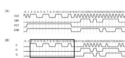
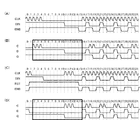
図2は、実施例1に係る制御信号生成部101、クロックゲーティングセル1021、及び、クロック供給装置1の動作を示すタイミングチャートである。
図2(A)は実施例1に係る制御信号生成部101の動作を示すタイミングチャートである。リセット期間、すなわちリセット信号RESETがHレベルの間は、カウンタ出力Q[1:0]はカウント動作によって毎クロックサイクル変化している。また、出力信号ENABLE_A、ENABLE_B、ENABLE_C、及び、ENABLE_Dは前述の通り、リセット期間はカウンタ出力値に応じてHレベルとLレベルを切り替えながら動作する。なお、出力信号ENABLE_A、ENABLE_B、ENABLE_C、及び、ENABLE_Dは前述の通り、通常動作期間、すなわちリセット信号RESETがLレベルの間は、Hレベルに固定される。また、リセット期間、すなわちリセット信号RESETがHレベルの間は、出力信号ENABLE_A、ENABLE_B、ENABLE_C、及び、ENABLE_DはそれぞれがHレベルとなるクロックサイクルが重ならないように動作するのが特徴である。
FIG. 2 is a timing chart illustrating operations of the control
FIG. 2A is a timing chart illustrating the operation of the control
図2(B)は実施例1に係るクロックゲーティングセル1021の動作を示すタイミングチャートである。入力信号ENBは、入力クロックCIがLレベルの間(即ち、入力クロックの反転信号EがHレベルの間)にラッチされてラッチの出力信号Qに反映される。出力クロックCOは、入力クロックCIと前記ラッチの出力信号Qとの論理積となり、結果としてクロックパルスが間引かれたものとなる。
FIG. 2B is a timing chart illustrating the operation of the
図2(C)は実施例1に係るクロック供給装置1の動作を示すタイミングチャートである。リセット信号がHレベルの間には、前述の通り複数の制御信号ENABLE_A、ENABLE_B、ENABLE_C、及び、ENABLE_Dが同時にHレベルにならないよう生成されている。また、出力クロック信号CLOCK_A、CLOCK_B、CLOCK_C、及び、CLOCK_Dは、複数の制御信号それぞれに応じてクロック信号CLOCKを間引いたものとなっている。出力クロック信号CLOCK_A、CLOCK_B、CLOCK_C、及び、CLOCK_Dは、リセット動作時にはそれぞれに、Hレベルとなるクロックサイクルが重ならないような異なるアクティブエッジ位相を持つクロックとなっている。つまり、出力クロック信号CLOCK_A、CLOCK_B、CLOCK_C、及び、CLOCK_Dはそれぞれ、異なるタイミングで立ち上がっている。
FIG. 2C is a timing chart illustrating the operation of the
また、リセット信号がLレベルの間には、前述の通り複数の制御信号ENABLE_A〜Dが同時にHレベルになり、出力クロック信号CLOCK_A〜Dは、クロック信号CLOCKそのものとなる。よって、出力クロック信号CLOCK_A〜Dは、通常動作時には、所定のアクティブエッジ位相を持つクロックとなっている。 While the reset signal is at the L level, the plurality of control signals ENABLE_A to D are simultaneously at the H level as described above, and the output clock signals CLOCK_A to D are the clock signal CLOCK itself. Therefore, the output clock signals CLOCK_A to D are clocks having a predetermined active edge phase during normal operation.
なお、回路ブロックA2、回路ブロックB3、回路ブロックC4、及び、回路ブロックD5は、リセット信号RESETをクロック信号に同期して参照する設計になっているため、これらの回路ブロックのリセット期間は図中のサイクル3〜サイクル28となる。
すなわち、クロック供給装置1は、回路ブロックA2〜D5の通常動作時には、回路ブロックA2〜D5に、所定のアクティブエッジ位相を持つクロック信号を供給する(第1のクロック供給)。また、クロック供給装置1は、回路ブロックA2〜D5のリセット動作時には、回路ブロックA2〜D5のそれぞれに、異なるアクティブエッジ位相を持つクロック信号を供給する(第2のクロック供給)。
Since the circuit block A2, the circuit block B3, the circuit block C4, and the circuit block D5 are designed to refer to the reset signal RESET in synchronization with the clock signal, the reset period of these circuit blocks is shown in the figure.
That is, the
図3は、図1に示した回路ブロックA2、回路ブロックB3、回路ブロックC4、及び、回路ブロックD5の内部に含まれるフリップフロップだけを示したブロック図である。
201、202、203、301、401、及び、501はフリップフロップである。前記フリップフロップと同図形で示したものは、符号を付けていないものも含めて全てフリップフロップである。説明のために、一部のフリップフロップだけに符号を付している。また、各フリップフロップの端子接続についてはフリップフロップ203とフリップフロップ501との接続だけを図示し、その他は省略している。
FIG. 3 is a block diagram showing only the flip-flops included in the circuit block A2, the circuit block B3, the circuit block C4, and the circuit block D5 shown in FIG.
回路ブロックA2は前述の通り、リセット信号RESETがHレベルの間はフリップフロップの初期化を行うが、フリップフロップ201、フリップフロップ202、及び、フリップフロップ203はそれぞれ初期化される手順が異なる。その詳細は後述する。フリップフロップ203のデータ入力端子には、回路ブロックD5のフリップフロップ501のデータ出力端子から出力されるデータ信号が接続されている。回路ブロックA2は前述の通り、リセット信号RESETがLレベルの間はクロック信号に同期して通常動作を行う。
As described above, the circuit block A2 initializes the flip-flop while the reset signal RESET is at the H level, but the flip-
回路ブロックB3も前述の通り、リセット信号RESETがHレベルの間はフリップフロップの初期化を行い、リセット信号RESETがLレベルの間はクロック信号に同期して通常動作を行う。回路ブロックC4も前述の通り、リセット信号RESETがHレベルの間はフリップフロップの初期化を行い、リセット信号RESETがLレベルの間はクロック信号に同期して通常動作を行う。 As described above, the circuit block B3 also initializes the flip-flop while the reset signal RESET is at the H level, and performs a normal operation in synchronization with the clock signal while the reset signal RESET is at the L level. As described above, the circuit block C4 also initializes the flip-flop while the reset signal RESET is at the H level, and performs a normal operation in synchronization with the clock signal while the reset signal RESET is at the L level.
回路ブロックD5も前述の通り、リセット信号RESETがHレベルの間はフリップフロップの初期化を行い、リセット信号RESETがLレベルの間はクロック信号に同期して通常動作を行う。なお、回路ブロックD5のフリップフロップ501のデータ出力端子から出力されるデータ信号は回路ブロックA2のフリップフロップ203のデータ入力端子に接続されている。
As described above, the circuit block D5 also initializes the flip-flop while the reset signal RESET is at the H level, and performs a normal operation in synchronization with the clock signal while the reset signal RESET is at the L level. The data signal output from the data output terminal of the flip-
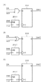
図4は、図3に示したフリップフロップ201、202、及び、203の接続構成を示すブロック図である。
図4(A)はフリップフロップ201の接続構成を示すブロック図である。図4(A)において、2011はクロックゲーティングセルで、クロックゲーティングセル1021と同じものである。
FIG. 4 is a block diagram showing a connection configuration of the flip-
FIG. 4A is a block diagram illustrating a connection configuration of the flip-
フリップフロップ201は、前述の「イネーブルによるクロックゲーティング技術」が適用されており、フリップフロップ201のクロック端子Cには、クロック信号CLKを制御信号ENBでクロックゲーティングしたクロックが入力される。フリップフロップ201のデータ入力端子Dには、データ信号DINとリセット信号RSTの反転信号との論理積信号が入力される。フリップフロップ201は、クロック端子Cに入力されるクロックの立ち上がりエッジのタイミングでデータ入力端子Dに入力されている値を保持し、保持している値をデータ出力端子Qからデータ信号DOUTとして出力する。リセット期間中、すなわちリセット信号RSTがHレベルの間は、データ入力端子DにはLレベルの値が入力されるので、クロック端子Cに入力されるクロック信号の立ち上がりエッジに同期して、フリップフロップ201の保持する値はLレベルに初期化される。
このフリップフロップ201のようにクロック信号の立ち上がりエッジに同期して、リセット信号の値で直接Lレベルに初期化されるフリップフロップを、同期リセット付きフリップフロップと呼ぶ。
The above-described “clock gating technology by enable” is applied to the flip-
A flip-flop that is directly initialized to the L level by the value of the reset signal in synchronization with the rising edge of the clock signal, such as the flip-
図4(B)はフリップフロップ202の接続構成を示すブロック図である。図4(B)において、2021はクロックゲーティングセルで、クロックゲーティングセル1021と同じものである。
FIG. 4B is a block diagram illustrating a connection configuration of the flip-
フリップフロップ202は、前述の「イネーブルによるクロックゲーティング技術」が適用されており、フリップフロップ202のクロック端子Cには、クロック信号CLKを制御信号ENBでクロックゲーティングしたクロックが入力される。フリップフロップ202のデータ入力端子Dには、データ信号DINとリセット信号RSTとの論理和信号が入力される。フリップフロップ202は、クロック端子Cに入力されるクロックの立ち上がりエッジのタイミングでデータ入力端子Dに入力されている値を保持し、保持している値をデータ出力端子Qからデータ信号DOUTとして出力する。リセット期間中、すなわちリセット信号RSTがHレベルの間は、データ入力端子DにはHレベルの値が入力されるので、クロック端子Cに入力されるクロック信号の立ち上がりエッジに同期して、フリップフロップ202の保持する値はHレベルに初期化される。
このフリップフロップ202のようにクロック信号の立ち上がりエッジに同期して、リセット信号の値で直接Hレベルに初期化されるフリップフロップを、同期セット付きフリップフロップと呼ぶ。
The above-described “clock gating technology by enable” is applied to the flip-
A flip-flop that is directly initialized to the H level by the value of the reset signal in synchronization with the rising edge of the clock signal like the flip-
図4(C)はフリップフロップ203の接続構成を示すブロック図である。図4(C)において、2031はクロックゲーティングセルで、クロックゲーティングセル1021と同じものである。
FIG. 4C is a block diagram illustrating a connection configuration of the flip-
フリップフロップ203は、前述の「イネーブルによるクロックゲーティング技術」が適用されており、フリップフロップ203のクロック端子Cには、クロック信号CLKを制御信号ENBでクロックゲーティングしたクロックが入力される。フリップフロップ203のデータ入力端子Dには、データ信号DINが入力される。フリップフロップ203は、クロック端子Cに入力されるクロックの立ち上がりエッジのタイミングでデータ入力端子Dに入力されている値を保持し、保持している値をデータ出力端子Qからデータ信号DOUTとして出力する。リセット期間中、すなわちリセット信号RSTがHレベルの間にも、データ入力端子Dに入力される値は直接は固定されず、入力データDINの値の生成に関係する他のフリップフロップが全て初期化された後に初期化値として固定されることになる。そして、その後のタイミングで、クロック端子Cに入力されるクロック信号の立ち上がりエッジに同期して、フリップフロップ203の保持する値は初期化される。
このフリップフロップ203のようにリセット信号の値で直接初期化されないフリップフロップを、リセットなしフリップフロップと呼ぶ。リセットなしフリップフロップを初期化できるタイミングは、前段のフリップフロップの初期化が全て完了した後で入力クロックの立ち上がりエッジが入力されるタイミングとなる。ここで、前段のフリップフロップとは、入力データDINの値を決定するのに関係する他のフリップフロップのことである(本実施例では回路ブロックD5のフリップフロップ501に対応する)。
The above-described “clock gating technique by enable” is applied to the flip-
A flip-flop that is not directly initialized with the value of the reset signal, such as the flip-
図5は、実施例1のクロック供給装置1により生成されるクロックによる、図4に示した回路、及び、フリップフロップ201、202、及び、203の動作を示すタイミングチャートである。
FIG. 5 is a timing chart illustrating the operation of the circuit illustrated in FIG. 4 and the flip-
図5(A)は図4(A)に示した回路の動作を示すタイミングチャートである。制御信号ENBは、前述の「イネーブルによるクロックゲーティング技術」のイネーブル制御を行う制御信号で、フリップフロップ201がラッチ動作すべき状態となるタイミングでHレベルとなっている。ここで、ラッチ動作すべき状態とは論理設計内容によって決まるものであるが、リセット信号がHレベルの間もラッチ動作すべき状態に含まれる。ラッチ動作すべき状態では、制御信号ENBはHレベルの値となっている。
FIG. 5A is a timing chart showing the operation of the circuit shown in FIG. The control signal ENB is a control signal for performing the enable control of the above-described “clock gating technique by enable”, and is at the H level at the timing when the flip-
クロック信号CLKは、リセット期間では前述の通りクロック信号CLOCKからクロックパルスを間引いたクロックになる。ここで、リセット信号RSTによるフリップフロップ201の初期化は前述の通りクロック同期で行われるため、リセット期間ではリセット信号がHレベルの期間を1クロックサイクルだけ後ろにずらした、サイクル2〜サイクル15の期間である。
The clock signal CLK becomes a clock obtained by thinning out clock pulses from the clock signal CLOCK as described above in the reset period. Here, the initialization of the flip-
図5(B)は図5(A)に示したタイミングチャートにおけるフリップフロップ201の動作を示すタイミングチャートである。フリップフロップ201のクロック端子Cに入力されるクロックは前述の通り、クロックゲーティングセル2011に入力されるクロック信号CLKを元にして、制御信号ENBに応じてクロックゲーティングセル2011がクロックゲーティングしたものとなる。そのため、制御信号ENBが常にHレベルとなるリセット期間にクロック端子Cに入力されるクロックは、クロック信号CLKそのままとなる。また、制御信号ENBが変化する通常動作期間にクロック端子Cに入力されるクロックは、図に示したようにクロック信号CLKからクロックパルスが間引かれたものになる。
リセット期間は図中の太線枠で囲んであるサイクル2〜サイクル15の期間であり、フリップフロップの初期化はサイクル2で行われているが、保持している値に変化はない。
FIG. 5B is a timing chart showing the operation of the flip-
The reset period is a period from
図5(C)は図4(B)に示した回路の動作を示すタイミングチャートである。図5(C)に示すように、制御信号ENBは、フリップフロップ202がラッチ動作すべき状態となるタイミングでHレベルとなっている。クロック信号CLKは、リセット期間では前述の通りクロック信号CLOCKからクロックパルスを間引いたクロックになる。
FIG. 5C is a timing chart showing the operation of the circuit shown in FIG. As shown in FIG. 5C, the control signal ENB is at the H level at a timing when the flip-
図5(D)は図5(C)に示したタイミングチャートにおけるフリップフロップ202の動作を示すタイミングチャートである。フリップフロップ202のクロックゲーティングセル接続構成は、フリップフロップ201と同様なので、クロック端子Cに入力されるクロックは図5(B)と同様にクロックゲーティングされたものとなる。リセット期間は、図中の太線枠で囲んであるサイクル2〜サイクル15の期間であり、フリップフロップの初期化はサイクル2に行われている。
FIG. 5D is a timing chart showing the operation of the flip-
図5(E)は図4(C)に示した回路の動作を示すタイミングチャートである。入力データ信号DINは、回路ブロックD5のフリップフロップ501の出力データ信号である。制御信号ENBは、フリップフロップ203がラッチ動作すべき状態となるタイミングでHレベルとなっている。クロック信号CLKは、リセット期間では前述の通りクロック信号CLOCKからクロックパルスを間引いたクロックになる。
FIG. 5E is a timing chart showing the operation of the circuit shown in FIG. The input data signal DIN is an output data signal of the flip-
図5(F)は図5(E)に示したタイミングチャートにおけるフリップフロップ203の動作を示すタイミングチャートである。フリップフロップ203のクロックゲーティングセル接続構成はフリップフロップ201と同様なので、クロック端子Cに入力されるクロックは図5(B)と同様にクロックゲーティングされたものとなる。
FIG. 5F is a timing chart showing the operation of the flip-
リセット期間は図中の太線枠で囲んであるサイクル2〜サイクル15の期間であり、フリップフロップの初期化はサイクル6に行われている。フリップフロップ203は前述の通り、リセットなしフリップフロップであるため、入力データ端子Dに入力される値がそのまま初期化値となる。そのため、フリップフロップ203を問題なく初期化するためには、前段のフリップフロップが全てリセット期間中に初期化されてその初期化値が確定する必要がある。ここで、フリップフロップ203の入力データ端子Dに入力されるデータ信号は、前述の通り回路ブロックD5のフリップフロップ501の出力データ信号である。そして、フリップフロップ501は図7(F)で後述するがリセット期間中のサイクル5に初期化が完了して確定するため、リセットなしフリップフロップであるフリップフロップ203を問題なく初期化することができる。
The reset period is a period from
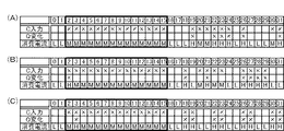
図6は、図5に示したタイミングチャートにおけるフリップフロップ201、202、及び、203の動作と消費電流の大きさを示した図である。
図6(A)は図5(B)に示したタイミングチャートにおけるフリップフロップ201の動作と消費電流の大きさを示した図である。消費電流値を上げる要素としては前述のように、ラッチ動作の有無とトグル動作の有無があるので、それぞれに対応するクロック端子Cへのクロックパルスの入力の有無とデータ出力端子Qから出力される値の変化の有無とをクロックサイクル毎の表にしてある。
FIG. 6 is a diagram showing the operation of the flip-
FIG. 6A illustrates the operation of the flip-
C入力の行は、クロック端子Cへのクロックパルスの入力の有無を表し、「×」マークは「有り」(入力有り)、空欄は「無し」(入力無し)を意味する。また、Q変化の行は、データ出力端子Qから出力される値の変化の有無を表し、「×」マークは「有り」(変化有り)、空欄は「無し」(変化無し)を意味する。 The C input row indicates whether or not a clock pulse is input to the clock terminal C. The “x” mark indicates “present” (input present), and the blank indicates “not present” (no input). The Q change row indicates whether or not the value output from the data output terminal Q has changed. The “x” mark indicates “present” (changed), and the blank indicates “not present” (no change).
消費電流の行は、フリップフロップ201及び図示しない周辺回路がクロック同期動作で消費する電流値の大きさを表している。消費電流の大きさは、前述したようにクロック端子Cへのクロックパルスの入力とデータ出力端子Qから出力される値の変化により決定され、次のように分類される。すなわち、C入力とQ出力の両方ともが「有り」のクロックサイクル、C入力のみ「有り」のクロックサイクル、どちらも「無し」のクロックサイクルに分類される。
The row of current consumption represents the magnitude of the current value consumed by the flip-
両方ともが有りのクロックサイクル、C入力のみ有りのクロックサイクル、どちらも無しのクロックサイクルの順序は、消費電流が大きい順であり、「H」、「M」、「L」で表記されている。なお、太線の枠で囲んだサイクル2〜サイクル15の間は、リセット期間を表している。
The order of the clock cycle with both, the clock cycle with only the C input, and the clock cycle without both is the order in which the current consumption is large and is indicated by “H”, “M”, “L”. . Note that a period between
図6(B)は図5(D)に示したタイミングチャートにおけるフリップフロップ202の動作と消費電流の大きさを示した表であり、図6(A)と同様に表記してある。
C入力の行とQ変化の行は図6(A)と同様に表記してある。消費電流の行は、フリップフロップ202及び図示しない周辺回路がクロック同期動作で消費する電流値の大きさを表している。消費電流の大きさは、図6(A)と同様に表記してある。
FIG. 6B is a table showing the operation of the flip-
The C input line and the Q change line are shown in the same manner as in FIG. The row of current consumption represents the magnitude of the current value consumed by the flip-
図6(C)は図5(F)に示したタイミングチャートにおけるフリップフロップ203の動作と消費電流の大きさを示した表であり、図6(A)と同様に表記してある。
C入力の行とQ変化の行は図6(A)と同様に表記してある。消費電流の行はフリップフロップ203及び図示しない周辺回路がクロック同期動作で消費する電流値の大きさを表している。消費電流の大きさは、図6(A)と同様に表記してある。
FIG. 6C is a table showing the operation of the flip-
The C input line and the Q change line are shown in the same manner as in FIG. The row of current consumption represents the magnitude of the current value consumed by the flip-
図7は、フリップフロップ301、401、及び、501の周辺回路の動作を示すタイミングチャートである。
図7(A)はフリップフロップ301の周辺回路の動作を示すタイミングチャートである。フリップフロップ301は、図4(A)で示したフリップフロップ201と同様の接続構成になっている。フリップフロップ301は、回路ブロックB3に含まれているため、フリップフロップ301の周辺回路にはクロック信号CLOCK_Bが入力される。そのため、本図は図5(A)に示したフリップフロップ201の周辺回路のタイミングチャートとはクロック信号CLKの波形が異なるものとなっている。
FIG. 7 is a timing chart showing the operation of the peripheral circuits of the flip-
FIG. 7A is a timing chart showing the operation of the peripheral circuit of the flip-
制御信号ENBは、フリップフロップ301がラッチ動作すべき状態となるタイミングでHレベルとなっている。クロック信号CLKは、リセット期間では前述の通りクロック信号CLOCKからクロックパルスを間引いたクロックになる。
The control signal ENB is at the H level at a timing when the flip-
図7(B)は図7(A)に示したタイミングチャートにおけるフリップフロップ301の動作を示すタイミングチャートである。フリップフロップ301のクロックゲーティングセル接続構成はフリップフロップ201と同様なので、クロック端子Cに入力されるクロックは図5(B)と同様にクロックゲーティングされたものとなる。リセット期間は、図中の太線枠で囲んであるサイクル2からサイクル15の期間であり、フリップフロップ301の初期化はサイクル3に行われている。
FIG. 7B is a timing chart showing the operation of the flip-
図7(C)はフリップフロップ401の周辺回路の動作を示すタイミングチャートである。フリップフロップ401は、図4(A)で示したフリップフロップ201と同様の接続構成になっている。フリップフロップ401は回路ブロックC4に含まれているため、クロック信号CLOCK_Cが入力される。そのため、本図は図5(A)に示したフリップフロップ201の周辺回路のタイミングチャートとはクロック信号CLKの波形が異なるものとなっている。制御信号ENBは、フリップフロップ401がラッチ動作すべき状態となるタイミングでHレベルとなっている。クロック信号CLKは、リセット期間では前述の通りクロック信号CLOCKからクロックパルスを間引いたクロックになる。
FIG. 7C is a timing chart showing the operation of the peripheral circuit of the flip-
図7(D)は図7(C)に示したタイミングチャートにおけるフリップフロップ401の動作を示すタイミングチャートである。フリップフロップ401のクロックゲーティングセル接続構成はフリップフロップ201と同様なので、クロック端子Cに入力されるクロックは図5(B)と同様にクロックゲーティングされたものとなる。リセット期間は図中の太線枠で囲んであるサイクル2〜サイクル15の期間であり、フリップフロップ401の初期化はサイクル4に行われているが、保持している値に変化はない。
FIG. 7D is a timing chart illustrating the operation of the flip-
図7(E)はフリップフロップ501の周辺回路の動作を示すタイミングチャートである。フリップフロップ501は、図4(A)で示したフリップフロップ201と同様の接続構成になっている。フリップフロップ501は回路ブロックD5に含まれているため、クロック信号CLOCK_Dが入力される。そのため、本図は図5(A)に示したフリップフロップ201の周辺回路のタイミングチャートとはクロック信号CLKの波形が異なるものとなっている。制御信号ENBは、フリップフロップ501がラッチ動作すべき状態となるタイミングでHレベルとなっている。クロック信号CLKは、リセット期間では前述の通りクロック信号CLOCKからクロックパルスを間引いたクロックになる。
FIG. 7E is a timing chart showing the operation of the peripheral circuit of the flip-
図7(F)は図7(E)に示したタイミングチャートにおけるフリップフロップ501の動作を示すタイミングチャートである。フリップフロップ501のクロックゲーティングセル接続構成はフリップフロップ201と同様なので、クロック端子Cに入力されるクロックは図5(B)と同様にクロックゲーティングされたものとなる。リセット期間は図中の太線枠で囲んであるサイクル2からサイクル15の期間であり、フリップフロップ501の初期化はサイクル5に行われている。出力データ端子Qから出力されたデータ信号DOUTは、フリップフロップ203の入力データ端子Dに接続されている。
FIG. 7F is a timing chart showing the operation of the flip-
図8は、図7に示したタイミングチャートにおけるフリップフロップ301、401、及び、501の動作と消費電流の大きさを示した図であり、図6と同様に表記してある。
図8(A)は図7(B)に示したタイミングチャートにおけるフリップフロップ301の動作と消費電流の大きさを示した表であり、図6(A)と同様に表記してある。
C入力の行とQ変化の行は図6(A)と同様に表記してある。消費電流の行は、フリップフロップ301及び図示しない周辺回路がクロック同期動作で消費する電流値の大きさを表している。消費電流の大きさは、図6(A)と同様に表記してある。
FIG. 8 is a diagram illustrating the operation of the flip-
FIG. 8A is a table showing the operation of the flip-
The C input line and the Q change line are shown in the same manner as in FIG. The row of current consumption represents the magnitude of the current value consumed by the flip-
図8(B)は図7(D)に示したタイミングチャートにおけるフリップフロップ401の動作と消費電流の大きさを示した表であり、図6(A)と同様に表記してある。
C入力の行とQ変化の行は図6(A)と同様に表記してある。消費電流の行は、フリップフロップ401及び図示しない周辺回路がクロック同期動作で消費する電流値の大きさを表している。消費電流の大きさは、図6(A)と同様に表記してある。
FIG. 8B is a table showing the operation of the flip-
The C input line and the Q change line are shown in the same manner as in FIG. The row of current consumption represents the magnitude of the current value consumed by the flip-
図8(C)は図7(F)に示したタイミングチャートにおけるフリップフロップ501の動作と消費電流の大きさを示した表であり、図6(A)と同様に表記してある。
C入力の行とQ変化の行は図6(A)と同様に表記してある。消費電流の行はフリップフロップ501及び図示しない周辺回路がクロック同期動作で消費する電流値の大きさを表している。消費電流の大きさは、図6(A)と同様に表記してある。
FIG. 8C is a table showing the operation of the flip-
The C input line and the Q change line are shown in the same manner as in FIG. The row of current consumption represents the magnitude of the current value consumed by the flip-
図9は、図3で示した各フリップフロップ及び周辺回路が通常動作期間中のあるクロックサイクルにおいて消費する電流値の大きさを示したブロック図である。ここで、あるクロックサイクルとは、図6及び図8におけるサイクル24である。また、図中の消費する電流値の大きさは、図6及び図8と同様に表記してある。
FIG. 9 is a block diagram showing the magnitude of the current value consumed by each flip-flop and peripheral circuit shown in FIG. 3 in a certain clock cycle during the normal operation period. Here, a certain clock cycle is the
回路ブロック内の全てのフリップフロップの消費電流値の合計値が、その回路ブロック全体での消費電流値となる。回路ブロック全体での消費電流値は回路ブロックの論理設計内容に応じて毎サイクル変化するものであるが、通常動作期間中で最も大きくなる値を、通常動作時の最大消費電流値と呼ぶ。この図の状態で、通常動作時の最大消費電流値となっているものとする。 A total value of current consumption values of all flip-flops in the circuit block is a current consumption value in the entire circuit block. The current consumption value in the entire circuit block changes every cycle in accordance with the logic design contents of the circuit block. The value that becomes the largest during the normal operation period is called the maximum current consumption value during the normal operation. In the state of this figure, it is assumed that the maximum current consumption value during normal operation is obtained.
図10は、図3で示した各フリップフロップ及び周辺回路がリセット期間中の初期化動作時のあるクロックサイクルにおいて消費する電流値の大きさを示したブロック図である。ここで、あるクロックサイクルとは、図6及び図8におけるサイクル2である。また、図中の消費する電流値の大きさは、図6及び図8と同様に表記してある。
FIG. 10 is a block diagram showing the magnitude of the current value consumed by each flip-flop and peripheral circuit shown in FIG. 3 in a certain clock cycle during the initialization operation during the reset period. Here, a certain clock cycle is
このクロックサイクルでは、回路ブロックA2のフリップフロップ全てにクロックが供給されているため、回路ブロックA2のフリップフロップ全てにおいてクロック端子Cへのクロックパルスの入力による電流が消費されている。また、初期化動作を行うフリップフロップは、さらにデータ出力端子Qから出力される値の変化による電流が消費されている。そのため、回路ブロックA2のフリップフロップは「H」又は「M」の消費電流値となっている。 In this clock cycle, since the clock is supplied to all the flip-flops in the circuit block A2, the current due to the input of the clock pulse to the clock terminal C is consumed in all the flip-flops in the circuit block A2. Further, the flip-flop that performs the initialization operation further consumes current due to a change in the value output from the data output terminal Q. For this reason, the flip-flop of the circuit block A2 has a consumption current value of “H” or “M”.
また、このクロックサイクルでは、回路ブロックB3、回路ブロックC4、及び、回路ブロックD5のフリップフロップは、クロックが供給されないため消費電流値は「L」となっている。 In this clock cycle, the flip-flops of the circuit block B3, the circuit block C4, and the circuit block D5 are not supplied with a clock, so that the current consumption value is “L”.
リセット期間中で回路ブロック全体での消費電流値が最も大きくなる値を、リセット動作時の最大消費電流値と呼ぶ。この図の状態で、リセット動作時の最大消費電流値となっている。 The value at which the current consumption value in the entire circuit block becomes the largest during the reset period is called the maximum current consumption value during the reset operation. In the state of this figure, the maximum current consumption value during the reset operation is obtained.
なお、リセット期間中の初期化動作時には、この図に示した状態の他に、回路ブロックB3、回路ブロックC4、又は、回路ブロックD5のいずれかだけにクロックが供給されるクロックサイクルも存在する。そのクロックサイクルとはそれぞれ、図6及び図8における、サイクル3、サイクル4、及び、サイクル5である。それらのクロックサイクルにおける状態は論理回路設計の内容によって決まるが、本実施例においては、図10に示した状態よりも「H」の消費電流値となるフリップフロップの数が少ないものとする。
In the initialization operation during the reset period, there is a clock cycle in which a clock is supplied only to one of the circuit block B3, the circuit block C4, or the circuit block D5 in addition to the state shown in FIG. The clock cycles are
図11は、図3で示した各フリップフロップ及び周辺回路がリセット期間中の初期化後の定常状態におけるあるクロックサイクルにおいて消費する電流値の大きさを示したブロック図である。ここで、あるクロックサイクルとは、図6及び図8におけるサイクル10である。また、図中の消費する電流値の大きさは、図6及び図8と同様に表記してある。
FIG. 11 is a block diagram showing the magnitude of the current value consumed in each clock cycle in the steady state after initialization by the flip-flops and peripheral circuits shown in FIG. 3 during the reset period. Here, a certain clock cycle is the
このサイクルでは、回路ブロックA2のフリップフロップ全てにクロックが供給されているため、回路ブロックA2のフリップフロップ全てにおいてクロック端子Cへのクロックパルスの入力による電流が消費されている。また、全てのフリップフロップが初期化された後であるため、データ出力端子Qから出力される値の変化による消費電流値の増加はない。そのため、回路ブロックA2のフリップフロップ全てが「M」の消費電流値となっている。 In this cycle, since the clock is supplied to all the flip-flops in the circuit block A2, the current due to the input of the clock pulse to the clock terminal C is consumed in all the flip-flops in the circuit block A2. Further, since all the flip-flops are initialized, there is no increase in the current consumption value due to a change in the value output from the data output terminal Q. Therefore, all the flip-flops of the circuit block A2 have the current consumption value “M”.
また、このサイクルでは、回路ブロックB3、回路ブロックC4、及び、回路ブロックD5のフリップフロップは、クロックが供給されないため消費電流値は「L」となっている。
リセット期間中で全てのフリップフロップが初期化された後の最大消費電流値を、リセット動作時の定常最大消費電流値と呼ぶ。この図の状態で、リセット動作時の定常最大消費電流値となっているものとする。
In this cycle, the flip-flops of the circuit block B3, the circuit block C4, and the circuit block D5 are not supplied with a clock, so that the current consumption value is “L”.
The maximum current consumption value after all flip-flops are initialized during the reset period is referred to as a steady maximum current consumption value during the reset operation. In the state of this figure, it is assumed that the steady-state maximum current consumption value during the reset operation is obtained.
なお、リセット期間中は、この図に示した状態の他に、回路ブロックB3、回路ブロックC4、又は、回路ブロックD5のいずれかだけにクロックが供給されるクロックサイクルも存在する。そのクロックサイクルとはそれぞれ、図6及び図8におけるサイクル11、サイクル12、及び、サイクル13である。それらのクロックサイクルにおける状態は論理回路設計によって決まるが、図11に示した状態と「M」や「L」の消費電流値となるフリップフロップの数が変わらないものとすると、消費電流値は図11に示したものと同じである。
During the reset period, there is a clock cycle in which a clock is supplied only to one of the circuit block B3, the circuit block C4, or the circuit block D5 in addition to the state shown in FIG. The clock cycles are
図12は、図6、図8、図9、図10、及び、図11で示した消費電流値「H」、「M」、及び、「L」について、実際の電流値との関係を表した図である。実際の消費電流値は回路ブロックを実装するデバイスに依存し、また、フリップフロップの周辺回路の内容によって変化するが、ここでは消費電流値の計算のため、モデル化した値を一意に割り当ててある。 FIG. 12 shows the relationship between the current consumption values “H”, “M”, and “L” shown in FIG. 6, FIG. 8, FIG. 9, FIG. FIG. The actual current consumption value depends on the device that implements the circuit block, and varies depending on the contents of the peripheral circuit of the flip-flop, but here the modeled value is uniquely assigned to calculate the current consumption value. .
図13は、図9、図10、及び図11で示した通常動作期間中の状態、リセット期間中の初期化動作時の状態、及び、初期化後の定常状態における消費電流値を表した図である。 FIG. 13 is a diagram showing the current consumption value in the normal operation period, the initialization operation state during the reset period, and the steady state after initialization shown in FIG. 9, FIG. 10, and FIG. It is.
図13(A)は図9で示した通常動作期間中の状態における消費電流値を表した図である。「H」が13個、「M」が18個、及び、「L」が25個ある状態なので、合計で244[pA]の消費電流値となる。前述の通り、この値が通常動作時の最大消費電流値である。 FIG. 13A shows the current consumption value in the state during the normal operation period shown in FIG. Since there are 13 “H”, 18 “M”, and 25 “L”, the current consumption value is 244 [pA] in total. As described above, this value is the maximum current consumption value during normal operation.
図13(B)は図10で示したリセット期間中の初期化動作時の状態における消費電流値を表した図である。「H」が6個、「M」が8個、及び、「L」が42個ある状態なので、合計で172[pA]の消費電流値となる。前述の通り、この値がリセット動作時の最大消費電流値である。 FIG. 13B shows a current consumption value in a state at the time of the initialization operation during the reset period shown in FIG. Since there are six “H”, eight “M”, and 42 “L”, the current consumption value is 172 [pA] in total. As described above, this value is the maximum current consumption value during the reset operation.
図13(C)は図11で示したリセット期間中の初期化後の定常状態における消費電流値を表した図である。「H」が0個、「M」が14個、及び、「L」が42個ある状態なので、合計で154[pA]の消費電流値となる。前述の通り、この値がリセット動作時の定常最大消費電流値である。 FIG. 13C is a diagram showing a current consumption value in a steady state after initialization during the reset period shown in FIG. Since there are 0 “H”, 14 “M”, and 42 “L”, the current consumption value is 154 [pA] in total. As described above, this value is the steady maximum current consumption value during the reset operation.
以上に示したように、リセット期間中にカウンタ値で生成したイネーブル信号によるクロックゲーティングを用いた回路で、クロック供給装置1を構成することができる。そして、クロック供給装置1によれば、リセットなしフリップフロップを含む複数の回路ブロック全体を確実にリセットすることができる(図5(F)のサイクル6)。また、リセット動作時の最大消費電流値を、通常動作時の最大消費電流値よりも小さくすることができる(図13)。
As described above, the
以下、本発明によるクロック供給装置との比較のために、従来のクロック供給装置を二例、図面を用いて説明する。
〔従来の第一のクロック供給装置〕
まず、従来の第一のクロック供給装置では、リセット動作時の最大消費電流値が、通常動作時の最大消費電流値よりも大きくなってしまうことを示す。なお、上述した実施例1のクロック供給装置と異なる構成の部分のみを以下に説明する。
Hereinafter, two conventional clock supply devices will be described with reference to the drawings for comparison with the clock supply device according to the present invention.
[First conventional clock supply device]
First, in the first conventional clock supply device, the maximum current consumption value during the reset operation is larger than the maximum current consumption value during the normal operation. Only the configuration different from that of the clock supply device of the first embodiment will be described below.
図25は、従来の第一のクロック供給装置の外部接続構成を示すブロック図である。
図25に示すように、従来のクロック供給装置は、この図に示すように配線のみで構成されており、実施例1のクロック供給装置1のように、制御信号生成部101やクロック制御部102は存在しない。
FIG. 25 is a block diagram showing an external connection configuration of a conventional first clock supply device.
As shown in FIG. 25, the conventional clock supply device is configured only by wiring as shown in this figure. Like the
図26は、従来の第一のクロック供給装置の動作を示すタイミングチャートである。
図26に示すように、従来の第一のクロック供給装置では、リセット期間中も各回路ブロックに入力するクロック信号CLOCKは変わらない。
FIG. 26 is a timing chart showing the operation of the conventional first clock supply device.
As shown in FIG. 26, in the conventional first clock supply device, the clock signal CLOCK input to each circuit block does not change even during the reset period.
図27は、従来の第一のクロック供給装置により入力されるクロックによる、図4に示した各回路、及び、フリップフロップ201、202、及び203の動作を示すタイミングチャートである。この図は上述した実施例1の図5に対応する図であり、リセット期間中のクロック信号CLKの動作が図5とは異なっている。
図27(A)は従来の第一のクロック供給装置により入力されるクロックによる、フリップフロップ201の周辺回路の動作を示すタイミングチャートである。この図は上述した実施例1の図5(A)に対応する図であり、リセット期間中のクロック信号CLKの動作が図5(A)とは異なっている。
FIG. 27 is a timing chart showing the operation of each circuit shown in FIG. 4 and the flip-
FIG. 27A is a timing chart showing the operation of the peripheral circuit of the flip-
図27(B)は図27(A)に示したタイミングチャートにおけるフリップフロップ201の動作を示すタイミングチャートである。この図は上述した実施例1の図5(B)に対応する図であり、リセット期間中のクロック信号CLKの動作が図5(B)とは異なっている。
FIG. 27B is a timing chart showing the operation of the flip-
図27(C)は従来の第一のクロック供給装置により入力されるクロックによる、図4(B)に示したフリップフロップ202の周辺回路の動作を示すタイミングチャートである。この図は上述した実施例1の図5(C)に対応する図であり、リセット期間中のクロック信号CLKの動作が図5(C)とは異なっている。
FIG. 27C is a timing chart showing the operation of the peripheral circuit of the flip-
図27(D)は図27(C)に示したタイミングチャートにおけるフリップフロップ202の動作を示すタイミングチャートである。この図は上述した実施例1の図5(D)に対応する図であり、リセット期間中のクロック信号CLKの動作が図5(D)とは異なっている。
FIG. 27D is a timing chart showing the operation of the flip-
図27(E)は従来の第一のクロック供給装置により入力されるクロックによる、図4(C)に示したフリップフロップ203の周辺回路の動作を示すタイミングチャートである。この図は上述した実施例1の図5(E)に対応する図であり、リセット期間中のクロック信号CLKの動作が図5(E)とは異なっている。
FIG. 27E is a timing chart showing the operation of the peripheral circuit of the flip-
図27(F)は図27(E)に示したタイミングチャートにおけるフリップフロップ203の動作を示すタイミングチャートである。この図は上述した実施例1の図5(F)に対応する図であり、リセット期間中のクロック信号CLKの動作が図5(F)とは異なっている。
FIG. 27F is a timing chart showing the operation of the flip-
図28は、図27に示したタイミングチャートにおけるフリップフロップ201、202、及び、203の動作と消費電流の大きさを示した図である。この図は上述した実施例1の図6に対応する図であり、リセット期間中のC入力の有無と消費電流の大きさが図6とは異なっている。
FIG. 28 is a diagram illustrating the operation of the flip-
図28(A)は図27(B)に示したタイミングチャートにおけるフリップフロップ201の動作と消費電流の大きさを示した図である。この図は上述した実施例1の図6(A)に対応する図であり、リセット期間中のC入力の有無と消費電流の大きさが図6(A)とは異なっている。
FIG. 28A illustrates the operation of the flip-
図28(B)は図27(D)に示したタイミングチャートにおけるフリップフロップ202の動作と消費電流の大きさを示した図である。この図は上述した実施例1の図6(B)に対応する図であり、リセット期間中のC入力の有無と消費電流の大きさが図6(B)とは異なっている。
FIG. 28B illustrates the operation of the flip-
図28(C)は図27(F)に示したタイミングチャートにおけるフリップフロップ203の動作と消費電流の大きさを示した図である。この図は上述した実施例1の図6(C)に対応する図であり、リセット期間中のC入力の有無と消費電流の大きさが図6(C)とは異なっている。
FIG. 28C is a diagram illustrating the operation of the flip-
従来の第一のクロック供給装置により入力されるクロックによる、フリップフロップ301、401、及び、501のタイミングチャート、動作、及び、消費電流の大きさについては図示しない。しかし、フリップフロップ301、401、及び、501のタイミングチャート、動作、及び、消費電流の大きさは、いずれも前述のフリップフロップ201、202、203と同様のものである。すなわち、従来の第一のクロック供給装置により入力されるクロックは、実施例1のクロック供給装置により入力されるクロックとは、リセット期間中のクロック信号CLKの動作が異なる。このため、リセット期間中の各フリップフロップのC入力の有無と消費電流の大きさも異なっている。
The timing chart, operation, and magnitude of current consumption of the flip-
図29は、従来の第一のクロック供給装置により入力されるクロックによる、図3で示した各フリップフロップ及び周辺回路がリセット期間中の初期化動作時のあるクロックサイクルにおいて消費する電流値の大きさを示したブロック図である。ここで、あるクロックサイクルとは、図28におけるサイクル2である。この図は上述した実施例1の図10に対応する図であり、「L」の消費電流値のフリップフロップが存在しないところが図10とは異なっている。
FIG. 29 shows the magnitude of the current value consumed by each flip-flop and the peripheral circuit shown in FIG. 3 in a clock cycle during the initialization operation during the reset period by the clock input by the conventional first clock supply device. It is the block diagram which showed this. Here, a certain clock cycle is
図30は、従来の第一のクロック供給装置により入力されるクロックによる、図3で示した各フリップフロップ及び周辺回路がリセット期間中の初期化後の定常状態におけるあるクロックサイクルにおいて消費する電流値の大きさを示したブロック図である。ここで、あるクロックサイクルとは、図28におけるサイクル10である。この図は上述した実施例1の図11に対応する図であり、「L」の消費電流値のフリップフロップが存在しないところが図11とは異なっている。
FIG. 30 shows a current value consumed in a certain clock cycle in a steady state after initialization by each of the flip-flops and peripheral circuits shown in FIG. 3 by a clock input by the conventional first clock supply device. It is the block diagram which showed the magnitude | size. Here, a certain clock cycle is
図31は、従来の第一のクロック供給装置により入力されるクロックによる、図29、及び、図30で示したリセット期間中の初期化動作時の状態、及び、初期化後の定常状態における消費電流値を表した図である。 FIG. 31 shows the state during the initialization operation during the reset period shown in FIG. 29 and FIG. 30 and the consumption in the steady state after initialization by the clock input by the conventional first clock supply device. It is a figure showing an electric current value.
図31(A)は、図29で示したリセット期間中の初期化動作時の状態における消費電流値を表した図である。「H」が6個、「M」が50個、及び、「L」が0個ある状態なので、合計で298[pA]の消費電流値となる。なお、通常動作時の最大消費電流値は、実施例1の場合と同じ値(図13(A)に示した244[pA])となる。 FIG. 31A is a diagram showing a current consumption value in the initialization operation state during the reset period shown in FIG. Since there are 6 “H”, 50 “M”, and 0 “L”, the current consumption is 298 [pA] in total. Note that the maximum current consumption value during normal operation is the same value as in the first embodiment (244 [pA] shown in FIG. 13A).
前述の通り、この値が従来の第一のクロック供給装置におけるリセット動作時の最大消費電流値であり、通常動作期間中の状態における消費電流値(244[pA])よりも大きくなってしまう。 As described above, this value is the maximum current consumption value during the reset operation in the first conventional clock supply device, and is larger than the current consumption value (244 [pA]) in the state during the normal operation period.
図31(B)は図30で示したリセット期間中の初期化後の定常状態における消費電流値を表した図である。「H」が0個、「M」が56個、及び、「L」が0個ある状態なので、合計で280[pA]の消費電流値となる。前述の通り、この値が従来の第一のクロック供給装置におけるリセット動作時の定常最大消費電流値であり、通常動作期間中の状態における消費電流値(244[pA])よりも大きくなってしまう。 FIG. 31B is a diagram showing the current consumption value in the steady state after initialization during the reset period shown in FIG. Since there are 0 “H”, 56 “M”, and 0 “L”, the current consumption is 280 [pA] in total. As described above, this value is the steady maximum current consumption value during the reset operation in the first conventional clock supply device, and is larger than the current consumption value (244 [pA]) in the state during the normal operation period. .
以上に示したように、従来の第一のクロック供給装置により各回路ブロックに入力されるクロックでは、リセット動作時の最大消費電流値が、通常動作時の最大消費電流値よりも大きくなってしまうことが明らかとなった。 As described above, in the clock input to each circuit block by the conventional first clock supply device, the maximum current consumption value during the reset operation becomes larger than the maximum current consumption value during the normal operation. It became clear.
〔従来の第二のクロック供給装置〕
次に、従来の第二のクロック供給装置について説明する。なお、上述した実施例1のクロック供給装置と異なる構成の部分のみを以下に説明する。
従来の第二のクロック供給装置は、リセット動作時に複数の回路ブロックのリセット期間を重複させないように、各回路ブロックに対し独立なクロックを入力するものである。従来の第二のクロック供給装置では、リセット期間中に全ての回路ブロックに同時にクロックを供給しないように制御することで、1クロックサイクルあたりの瞬間的な消費電流を削減可能である。
[Conventional second clock supply device]
Next, a conventional second clock supply device will be described. Only the configuration different from that of the clock supply device of the first embodiment will be described below.
The conventional second clock supply device inputs an independent clock to each circuit block so that the reset periods of the plurality of circuit blocks do not overlap during the reset operation. In the conventional second clock supply device, instantaneous current consumption per clock cycle can be reduced by controlling not to supply clocks to all circuit blocks simultaneously during the reset period.
図32は、従来の第二のクロック供給装置の動作を示すタイミングチャートである。
従来の第二のクロック供給装置では、リセット信号がHレベルの間には、複数の制御信号ENABLE_A、ENABLE_B、ENABLE_C、及び、ENABLE_Dが同時にHレベルにならないよう生成されている。また、出力クロック信号CLOCK_A、CLOCK_B、CLOCK_C、及び、CLOCK_Dは、複数の制御信号それぞれに応じてクロック信号を間引いたものとなっている。この図は、上述した実施例1の図2(C)に対応する図であり、各回路ブロックに対して個別にリセット期間を設けるようにクロック信号を生成しているところが図2(C)とは異なっている。
FIG. 32 is a timing chart showing the operation of the conventional second clock supply device.
In the conventional second clock supply device, while the reset signal is at the H level, the plurality of control signals ENABLE_A, ENABLE_B, ENABLE_C, and ENABLE_D are generated so as not to simultaneously become the H level. The output clock signals CLOCK_A, CLOCK_B, CLOCK_C, and CLOCK_D are obtained by thinning out clock signals according to each of a plurality of control signals. This diagram corresponds to FIG. 2C of the first embodiment described above, and FIG. 2C shows that a clock signal is generated so that a reset period is individually provided for each circuit block. Is different.
図33は、従来の第二のクロック供給装置により入力されるクロックによる、フリップフロップ203の周辺回路、フリップフロップ203、フリップフロップ501の周辺回路、及びフリップフロップ501の動作を示すタイミングチャートである。
図33(A)は従来の第二のクロック供給装置により入力されるクロックによる、フリップフロップ203の周辺回路の動作を示すタイミングチャートである。この図は上述した実施例1の図5(E)に対応する図であり、リセット期間中のクロック信号CLKの動作が図5(E)とは異なっている。入力データ信号DINは、フリップフロップ501の出力データ信号である。
FIG. 33 is a timing chart showing the operation of the peripheral circuit of the flip-
FIG. 33A is a timing chart showing the operation of the peripheral circuit of the flip-
図33(B)は図33(A)に示したタイミングチャートにおけるフリップフロップ203の動作を示すタイミングチャートである。
リセット期間は図中の太線枠で囲んであるサイクル2〜サイクル15の期間であり、フリップフロップ203の初期化はサイクル2、3、及び、4に行われている。フリップフロップ203は前述の通りリセットなしフリップフロップであるため、入力データ端子に入力される値がそのまま初期化値となる。そのため、フリップフロップ203を問題なく初期化するためには、前段のフリップフロップが全てリセット期間中に初期化されてその初期化値が確定する必要がある。ここで、フリップフロップ203の入力データ端子Cに入力されるデータ信号は前述の通りフリップフロップ501の出力データ信号である。そして、フリップフロップ501は後述するがリセット期間中のサイクル11に初期化が完了して確定する。よって、従来の第二のクロック供給装置により入力されるクロックでは、前段のフリップフロップ501の初期化値が確定するサイクル11より前に初期化を行う、リセットなしフリップフロップであるフリップフロップ203を初期化できていない。
FIG. 33B is a timing chart showing the operation of the flip-
The reset period is a period from
図33(C)は従来の第二のクロック供給装置により入力されるクロックによる、フリップフロップ501の周辺回路の動作を示すタイミングチャートである。この図は上述した実施例1の図7(E)に対応する図であり、リセット期間中のクロック信号CLKの動作が図7(E)とは異なっている。
FIG. 33C is a timing chart showing the operation of the peripheral circuit of the flip-
図33(D)は図33(C)に示したタイミングチャートにおけるフリップフロップ501の動作を示すタイミングチャートである。
リセット期間は図中の太線枠で囲んであるサイクル2〜サイクル15の期間であり、フリップフロップ501の初期化はサイクル11に行われている。フリップフロップ501の出力データ端子Qから出力されたデータ信号DOUTは、フリップフロップ203の入力データ端子Dに接続されている。このように、リセットなしフリップフロップであるフリップフロップ203の初期化を行うサイクル2、3及び4より後に前段のフリップフロップ501の初期化値が確定している。
以上に示したように、従来の第二のクロック供給装置により入力されるクロックにより、複数の回路ブロックのリセット期間を独立にすると、完全なリセットができなくなることが明らかになった(図33)。
FIG. 33D is a timing chart illustrating the operation of the flip-
The reset period is a period from
As described above, it has been clarified that when the reset period of the plurality of circuit blocks is made independent by the clock input from the conventional second clock supply device, complete reset cannot be performed (FIG. 33). .
以上のように、実施例1のクロック供給装置では、複数の回路ブロック全体のピーク消費電流を軽減しつつ、複数の回路ブロック全体のリセットを適切に行えるクロックを複数の回路ブロックに入力することができる。その結果、LSI電源の設計と製造のコストを抑えることができる。 As described above, in the clock supply apparatus according to the first embodiment, a clock that can appropriately reset the entire plurality of circuit blocks can be input to the plurality of circuit blocks while reducing the peak current consumption of the entire plurality of circuit blocks. it can. As a result, the LSI power supply design and manufacturing costs can be reduced.
以下、本発明の実施例2を示すクロック供給装置の構成について図面を用いて説明する。なお、ここでは、実施例1と異なる箇所のみを説明する。
実施例2のクロック供給装置は、実施例1のクロック供給装置の制御信号生成部101を、図14で示す別の構成の制御信号生成部に置き換えたものとなる。
図14は、実施例2の制御信号生成部101の内部構成を示すブロック図である。
図14において、1012は非同期セット付きフリップフロップである。また、1013、1014、及び、1015は非同期リセット付きフリップフロップである。
非同期セット付きフリップフロップ1012は、クロック信号CLOCK、リセット信号RESET、入力信号E_D、及び、出力信号E_Aの各信号線と接続されている。非同期セット付きフリップフロップ1012は、データラッチ動作をクロック信号に同期して、また、初期化動作をクロック信号に非同期で行う。非同期セット付きフリップフロップ1012は、リセット信号を受信し、リセット信号がLレベルの間(通常動作時)は保持する値をHレベル(非アクティブレベル)に初期化する。非同期セット付きフリップフロップ1012は、リセット信号がHレベルの間はクロック信号に同期してデータ入力端子Dに入力されている入力信号E_Dの値を内部に保持してデータ出力端子Qから出力信号E_Aとして出力する。
Hereinafter, the configuration of the clock supply apparatus showing the second embodiment of the present invention will be described with reference to the drawings. Here, only different points from the first embodiment will be described.
The clock supply apparatus according to the second embodiment is obtained by replacing the control
FIG. 14 is a block diagram illustrating an internal configuration of the control
In FIG. 14,
The flip-
非同期リセット付きフリップフロップ1013は、クロック信号CLOCK、リセット信号RESET、入力信号E_A、及び出力信号E_Bの各信号線と接続されている。非同期リセット付きフリップフロップ1013は、データラッチ動作をクロック信号に同期して、また、初期化動作をクロック信号に非同期で行う。非同期リセット付きフリップフロップ1013は、リセット信号を受信し、リセット信号がLレベルの間(通常動作時)は保持する値をLレベル(非アクティブレベル)に初期化する。非同期リセット付きフリップフロップ1013は、リセット信号がHレベルの間はクロック信号に同期してデータ入力端子Dに入力されている入力信号E_Aの値を内部に保持してデータ出力端子Qから出力信号E_Bとして出力する。
The flip-
非同期リセット付きフリップフロップ1014は、クロック信号CLOCK、リセット信号RESET、入力信号E_B、及び出力信号E_Cの各信号線と接続されている。非同期リセット付きフリップフロップ1014は、データラッチ動作をクロック信号に同期して、また、初期化動作をクロック信号に非同期で行う。非同期リセット付きフリップフロップ1014は、リセット信号を受信し、リセット信号がLレベルの間は保持する値をLレベルに初期化する。非同期リセット付きフリップフロップ1014は、リセット信号がHレベルの間はクロック信号に同期してデータ入力端子Dに入力されている入力信号E_Bの値を内部に保持してデータ出力端子Qから出力信号E_Cとして出力する。
The flip-
非同期リセット付きフリップフロップ1015は、クロック信号CLOCK、リセット信号RESET、入力信号E_C、及び出力信号E_Dの各信号線と接続されている。非同期リセット付きフリップフロップ1015は、データラッチ動作をクロック信号に同期して、また、初期化動作をクロック信号に非同期で行う。非同期リセット付きフリップフロップ1015はリセット信号を受信し、リセット信号がLレベルの間は保持する値をLレベルに初期化する。非同期リセット付きフリップフロップ1015は、リセット信号がHレベルの間はクロック信号に同期してデータ入力端子Dに入力されている入力信号E_Cの値を内部に保持してデータ出力端子Qから出力信号E_Dとして出力する。
The flip-
出力信号ENABLE_Aは、リセット信号がLレベルのとき、又は、出力信号E_AがHレベルのときにHレベル、それ以外のときにLレベルとなる。出力信号ENABLE_Bは、リセット信号がLレベルのとき、又は、出力信号E_BがHレベルのときにHレベル、それ以外のときにLレベルとなる。出力信号ENABLE_Cは、リセット信号がLレベルのときか、又は、出力信号E_CがHレベルのときにHレベル、それ以外のときにLレベルとなる。出力信号ENABLE_Dは、リセット信号がLレベルのときか、又は、出力信号E_DがHレベルのときにHレベル、それ以外のときにLレベルとなる。
すなわち、実施例2の制御信号生成部101は、フリップフロップ1012〜1015が直列かつ環状に接続された回路有し、リセット動作時に、フリップフロップ1012〜1015の出力信号をENABLE_A〜Dとして出力する。
The output signal ENABLE_A is H level when the reset signal is L level or when the output signal E_A is H level, and is L level otherwise. The output signal ENABLE_B becomes H level when the reset signal is L level or when the output signal E_B is H level, and becomes L level otherwise. The output signal ENABLE_C is H level when the reset signal is L level or the output signal E_C is H level, and is L level otherwise. The output signal ENABLE_D becomes H level when the reset signal is L level or when the output signal E_D is H level, and becomes L level otherwise.
That is, the control
実施例2の制御信号生成部101、クロックゲーティングセル1021、及びクロック供給装置1の動作を示すタイミングチャートは、実施例1の図2(A)のタイミングチャートを図15に示すタイミングチャートに置き換えたものとなる。すなわち、図2(B),図2(C)に示したタイミングチャートは実施例1と同一である。
The timing chart showing the operation of the control
図15は、実施例2に係る制御信号生成部101の動作を示すタイミングチャートである。
リセット期間、すなわちリセット信号RESETがHレベルの間は、出力信号E_A、E_B、E_C、及び、E_Dは、4つのフリップフロップ1012、1013、1014、及び1015の動作によって伝播動作している。
FIG. 15 is a timing chart illustrating the operation of the control
During the reset period, that is, while the reset signal RESET is at the H level, the output signals E_A, E_B, E_C, and E_D are propagated by the operations of the four flip-
また、出力信号ENABLE_A、ENABLE_B、ENABLE_C、及び、ENABLE_Dは前述の通り、リセット期間ではE_A、E_B、E_C、及び、E_Dのレベルに応じてHレベルとLレベルを切り替えながら動作する。 Further, as described above, the output signals ENABLE_A, ENABLE_B, ENABLE_C, and ENABLE_D operate while switching between the H level and the L level according to the levels of E_A, E_B, E_C, and E_D in the reset period.
また、出力信号ENABLE_A、ENABLE_B、ENABLE_C、及び、ENABLE_Dは前述の通り、通常動作期間、すなわちリセット信号RESETがLレベルの間は、Hレベルに固定される。 Further, as described above, the output signals ENABLE_A, ENABLE_B, ENABLE_C, and ENABLE_D are fixed at the H level during the normal operation period, that is, while the reset signal RESET is at the L level.
なお、リセット期間すなわちリセット信号RESETがHレベルの間では、出力信号ENABLE_A、ENABLE_B、ENABLE_C、及び、ENABLE_DそれぞれがHレベルとなるクロックサイクルが重ならないように動作するのが特徴である。出力信号ENABLE_A、ENABLE_B、ENABLE_C、及び、ENABLE_Dは、実施例1の図2(A)と同じ波形となっている。 Note that, during the reset period, that is, while the reset signal RESET is at the H level, the output signals ENABLE_A, ENABLE_B, ENABLE_C, and ENABLE_D operate so as not to overlap each other in the clock cycle. The output signals ENABLE_A, ENABLE_B, ENABLE_C, and ENABLE_D have the same waveforms as those in FIG.
以上、実施例2に示すように、リセット期間中に、直列接続したフリップフロップで生成したイネーブル信号によるクロックゲーティングを用いた回路で、本発明のクロック供給装置1を構成することができる。実施例2のクロック供給装置1によれば、リセットなしフリップフロップを含む複数の回路ブロック全体を確実にリセットすることができる(図5(F)のサイクル6)。また、リセット動作時の最大消費電流値を、通常動作時の最大消費電流値よりも小さくすることができる(図13)。
As described above, as shown in the second embodiment, the
すなわち、実施例2のクロック供給装置によれば、複数の回路ブロック全体のピーク消費電流を軽減しつつ、複数の回路ブロック全体のリセットを適切に行えるクロックを複数の回路ブロックに入力することができる。その結果、LSI電源の設計と製造のコストを抑えることができる。 That is, according to the clock supply device of the second embodiment, a clock that can appropriately reset the entire plurality of circuit blocks can be input to the plurality of circuit blocks while reducing the peak current consumption of the entire plurality of circuit blocks. . As a result, the LSI power supply design and manufacturing costs can be reduced.
以下、本発明の実施例3を示すクロック供給装置の構成について図面を用いて説明する。なお、ここでは、実施例1と異なる箇所のみを説明する。
実施例3のクロック供給装置は、実施例1のクロック供給装置の内部構成を図16で示す別の構成に置き換えたものとなる。
図16は、実施例3のクロック供給装置1の内部構成を示すブロック図である。
図16において、6はクロック生成部A、7はクロック生成部B、8はクロック生成部C、9はクロック生成部Dである。
601は制御信号生成部A、602はクロック制御部である。701は制御信号生成部B、702はクロック制御部である。801は制御信号生成部C、802はクロック制御部である。901は制御信号生成部D、902はクロック制御部である。
Hereinafter, the configuration of the clock supply apparatus showing the third embodiment of the present invention will be described with reference to the drawings. Here, only different points from the first embodiment will be described.
The clock supply device of the third embodiment is obtained by replacing the internal configuration of the clock supply device of the first embodiment with another configuration shown in FIG.
FIG. 16 is a block diagram illustrating an internal configuration of the
In FIG. 16, 6 is a clock generator A, 7 is a clock generator B, 8 is a clock generator C, and 9 is a clock generator D.
6011、7011、8011、及び9011は、制御信号生成部で、実施例1の制御信号生成部101と同じものである。6021はクロックゲーティングセルで、実施例1のクロックゲーティングセル1021と同じものである。
実施例3のクロック供給装置1は、4つのクロック生成部(クロック生成部A6、クロック生成部B7、クロック生成部C8、及び、クロック生成部D9)から構成される。これら4つのクロック生成部は、それぞれ独立にクロック信号を生成するが、共通のリセット信号RESETによって同期して内部の動作を制御するのが特徴である。
The
クロック生成部A6は、クロック信号CLOCK、リセット信号RESET、及び、出力信号CLOCK_Aの各信号線と接続されており、クロック信号に同期して動作する。クロック生成部A6は、リセット信号を受信し、リセット信号がLレベルの間は通常動作期間、また、Hレベルの間はリセット期間であると認識して動作する。クロック生成部A6は、出力信号CLOCK_Aを出力する。 The clock generation unit A6 is connected to each signal line of the clock signal CLOCK, the reset signal RESET, and the output signal CLOCK_A, and operates in synchronization with the clock signal. The clock generation unit A6 receives the reset signal and operates by recognizing that it is a normal operation period while the reset signal is at the L level and a reset period when the reset signal is at the H level. The clock generation unit A6 outputs an output signal CLOCK_A.
クロック生成部B7は、クロック信号CLOCK、リセット信号RESET、及び、出力信号CLOCK_Bの各信号線と接続されており、クロック信号に同期して動作する。クロック生成部B7は、リセット信号を受信し、リセット信号がLレベルの間は通常動作期間、また、Hレベルの間はリセット期間であると認識して動作する。クロック生成部B7は出力信号CLOCK_Bを出力する。 The clock generator B7 is connected to each signal line of the clock signal CLOCK, the reset signal RESET, and the output signal CLOCK_B, and operates in synchronization with the clock signal. The clock generation unit B7 receives the reset signal and operates by recognizing that it is a normal operation period while the reset signal is at the L level and a reset period when the reset signal is at the H level. The clock generation unit B7 outputs an output signal CLOCK_B.
クロック生成部C8は、クロック信号CLOCK、リセット信号RESET、及び、出力信号CLOCK_Cの各信号線と接続されており、クロック信号に同期して動作する。クロック生成部C8は、リセット信号を受信し、リセット信号がLレベルの間は通常動作期間、また、Hレベルの間はリセット期間であると認識して動作する。クロック生成部C8は出力信号CLOCK_Cを出力する。 The clock generation unit C8 is connected to each signal line of the clock signal CLOCK, the reset signal RESET, and the output signal CLOCK_C, and operates in synchronization with the clock signal. The clock generation unit C8 receives the reset signal and operates by recognizing that it is a normal operation period while the reset signal is at the L level and a reset period when the reset signal is at the H level. The clock generation unit C8 outputs an output signal CLOCK_C.
クロック生成部D9は、クロック信号CLOCK、リセット信号RESET、及び、出力信号CLOCK_Dの各信号線と接続されており、クロック信号に同期して動作する。クロック生成部D9は、リセット信号を受信し、リセット信号がLレベルの間は通常動作期間、また、Hレベルの間はリセット期間であると認識して動作する。クロック生成部D9は出力信号CLOCK_Dを出力する。 The clock generation unit D9 is connected to each signal line of the clock signal CLOCK, the reset signal RESET, and the output signal CLOCK_D, and operates in synchronization with the clock signal. The clock generation unit D9 receives the reset signal and operates by recognizing that it is a normal operation period while the reset signal is at the L level and a reset period when the reset signal is at the H level. The clock generation unit D9 outputs an output signal CLOCK_D.
制御信号生成部A601は、クロック信号CLOCKの信号線、リセット信号RESETの信号線、及び、クロック制御部602と接続されており、クロック信号に同期して動作する。制御信号生成部A601は、リセット信号を受信し、リセット信号がLレベルの間は通常動作期間、また、Hレベルの間はリセット期間であると認識して動作する。制御信号生成部A601は、クロック制御部602に対して制御信号ENABLE_Aを送信する。
The control signal generation unit A601 is connected to the signal line of the clock signal CLOCK, the signal line of the reset signal RESET, and the
クロック制御部602は、クロック信号CLOCKの信号線、制御信号生成部A601、及び、出力クロック信号CLOCK_Aの信号線と接続されている。クロック制御部602はクロック信号を使用して動作する。クロック制御部602は、制御信号生成部A601から出力される制御信号ENABLE_Aに応じて、出力クロック信号CLOCK_Aを出力する。
The
制御信号生成部B701は、クロック信号CLOCKの信号線、リセット信号RESETの信号線、及び、クロック制御部702と接続されており、クロック信号に同期して動作する。制御信号生成部B701はリセット信号を受信し、リセット信号がLレベルの間は通常動作期間、また、Hレベルの間はリセット期間であると認識して動作する。制御信号生成部B701は、クロック制御部702に対して制御信号ENABLE_Bを送信する。
The control signal
クロック制御部702は、クロック信号CLOCKの信号線、制御信号生成部B701、及び、出力クロック信号CLOCK_Bの信号線と接続されている。クロック制御部702はクロック信号を使用して動作する。クロック制御部702は、制御信号生成部B701から出力される制御信号ENABLE_Bに応じて、出力クロック信号CLOCK_Bを出力する。
The
制御信号生成部C801は、クロック信号CLOCKの信号線、リセット信号RESETの信号線、及び、クロック制御部802と接続されており、クロック信号に同期して動作する。制御信号生成部C801はリセット信号を受信し、リセット信号がLレベルの間は通常動作期間、また、Hレベルの間はリセット期間であると認識して動作する。制御信号生成部C801はクロック制御部802に対して制御信号ENABLE_Cを送信する。
The control signal generation unit C801 is connected to the signal line of the clock signal CLOCK, the signal line of the reset signal RESET, and the
クロック制御部802は、クロック信号CLOCKの信号線、制御信号生成部C801、及び、出力クロック信号CLOCK_Cの信号線と接続されている。クロック制御部802はクロック信号を使用して動作する。クロック制御部802は、制御信号生成部C801から出力される制御信号ENABLE_Cに応じて、出力クロック信号CLOCK_Cを出力する。
The
制御信号生成部D901は、クロック信号CLOCKの信号線、リセット信号RESETの信号線、及び、クロック制御部902と接続されており、クロック信号に同期して動作する。制御信号生成部D901はリセット信号を受信し、リセット信号がLレベルの間は通常動作期間、また、Hレベルの間はリセット期間であると認識して動作する。制御信号生成部D901はクロック制御部902に対して制御信号ENABLE_Dを送信する。
The control signal generation unit D901 is connected to the signal line of the clock signal CLOCK, the signal line of the reset signal RESET, and the
クロック制御部902は、クロック信号CLOCKの信号線、制御信号生成部D901、及び、出力クロック信号CLOCK_Dの信号線と接続されている。クロック制御部902はクロック信号を使用して動作する。クロック制御部902は、制御信号生成部D901から出力される制御信号ENABLE_Dに応じて、出力クロック信号CLOCK_Dを出力する。
The
制御信号生成部6011は、クロック信号CLOCK、リセット信号RESET、及び、出力信号ENABLE_Aの各信号線と接続されており、クロック信号に同期して動作する。制御信号生成部6011はリセット信号を受信し、リセット信号がLレベルの間は通常動作期間、また、Hレベルの間はリセット期間であると認識して動作する。制御信号生成部6011は、出力信号線ENABLE_Aに対して制御信号ENABLE_Aを送信する。
The control
制御信号生成部7011は、クロック信号CLOCK、リセット信号RESET、及び、出力信号ENABLE_Bの各信号線と接続されており、クロック信号に同期して動作する。制御信号生成部7011はリセット信号を受信し、リセット信号がLレベルの間は通常動作期間、また、Hレベルの間はリセット期間であると認識して動作する。制御信号生成部7011は、出力信号線ENABLE_Bに対して制御信号ENABLE_Bを送信する。
The control
制御信号生成部8011は、クロック信号CLOCK、リセット信号RESET、及び、出力信号ENABLE_Cと接続されており、クロック信号に同期して動作する。制御信号生成部8011はリセット信号を受信し、リセット信号がLレベルの間は通常動作期間、また、Hレベルの間はリセット期間であると認識して動作する。制御信号生成部8011は、出力信号線ENABLE_Cに対して制御信号ENABLE_Cを送信する。
The control
制御信号生成部9011は、クロック信号CLOCK、リセット信号RESET、及び、出力信号ENABLE_Dと接続されており、クロック信号に同期して動作する。制御信号生成部9011はリセット信号を受信し、リセット信号がLレベルの間は通常動作期間、また、Hレベルの間はリセット期間であると認識して動作する。制御信号生成部9011は、出力信号線ENABLE_Dに対して制御信号ENABLE_Dを送信する。
The control
クロックゲーティングセル6021は、クロック信号CLOCK、入力信号ENABLE_A、及び、出力クロック信号CLOCK_Aの各信号線とそれぞれCI、ENB、及び、CO端子で接続されている。クロックゲーティングセル7021は、クロック信号CLOCK、入力信号ENABLE_B、及び、出力クロック信号CLOCK_Bの各信号線とそれぞれCI、ENB、及び、CO端子で接続されている。クロックゲーティングセル8021は、クロック信号CLOCK、入力信号ENABLE_C、及び、出力クロック信号CLOCK_Cの各信号線とそれぞれCI、ENB、及び、CO端子で接続されている。クロックゲーティングセル9021は、クロック信号CLOCK、入力信号ENABLE_D、及び、出力クロック信号CLOCK_Dの各信号線とそれぞれCI、ENB、及び、CO端子で接続されている。
The
クロックゲーティングセル6021は、クロック信号CLOCKに含まれるクロックパルスを入力信号ENBに応じて間引いて出力信号COとして出力する動作を行う。クロック制御部702、クロック制御部802、及び、クロック制御部902は、クロック制御部602と同じものである。
The
他の構成は実施例1と同じである。すなわち、実施例3のクロック供給装置1から複数の回路ブロックA2、B3、C4、及び、D5に入力される、クロック信号CLOCK_A、CLOCK_B、CLOCK_C、及び、CLOCK_Dは、実施例1の図2(C)と同じ波形となる。
Other configurations are the same as those of the first embodiment. That is, the clock signals CLOCK_A, CLOCK_B, CLOCK_C, and CLOCK_D input to the plurality of circuit blocks A2, B3, C4, and D5 from the
以上、実施例3に示すように、リセット期間中に、カウンタ値で生成したイネーブル信号によるクロックゲーティングを複数回路で、本発明のクロック供給装置1を構成することができる。実施例3のクロック供給装置1によれば、リセットなしフリップフロップを含む複数の回路ブロック全体を確実にリセットすることができる(図5(F)のサイクル6)。また、リセット動作時の最大消費電流値を、通常動作時の最大消費電流値よりも小さくすることができる(図13)。
As described above, as shown in the third embodiment, the
すなわち、実施例3のクロック供給装置によれば、複数の回路ブロック全体のピーク消費電流を軽減しつつ、複数の回路ブロック全体のリセットを適切に行えるクロックを複数の回路ブロックに入力することができる。その結果、LSI電源の設計と製造のコストを抑えることができる。 That is, according to the clock supply device of the third embodiment, a clock that can appropriately reset the entire plurality of circuit blocks can be input to the plurality of circuit blocks while reducing the peak current consumption of the entire plurality of circuit blocks. . As a result, the LSI power supply design and manufacturing costs can be reduced.
以下、本発明の実施例4のクロック供給装置の構成について図面を用いて説明する。なお、ここでは、実施例1と異なる箇所のみを説明する。
実施例4のクロック供給装置は、実施例1のクロック供給装置のクロック制御部102を、図17で示す別の構成のクロック制御部103に置き換えたものとなる。
図17は、実施例4のクロック供給装置1の内部構成を示すブロック図である。
制御信号生成部101は、実施例1の制御信号生成部101(図1)と同じもの、又は、実施例2の制御信号生成部101(図14)と同じものである。103は実施例4のクロック制御部である。1031、1032、1033、及び、1034はセレクタである。
The configuration of the clock supply apparatus according to the fourth embodiment of the present invention will be described below with reference to the drawings. Here, only different points from the first embodiment will be described.
The clock supply apparatus according to the fourth embodiment is obtained by replacing the
FIG. 17 is a block diagram illustrating an internal configuration of the
The control
制御信号生成部101は、クロック信号CLOCKの信号線、リセット信号RESETの信号線、及び、クロック制御部103と接続されており、クロック信号に同期して動作する。制御信号生成部101は、リセット信号を受信し、リセット信号がLレベルの間は通常動作期間、また、Hレベルの間はリセット期間であると認識して動作する。制御信号生成部101は、クロック制御部103に対して複数の制御信号ENABLE_A、ENABLE_B、ENABLE_C、及び、ENABLE_Dを送信する。
The control
クロック制御部103は、クロック信号CLOCKの信号線、リセット信号RESETの信号線、制御信号生成部101、及び、出力クロック信号CLOCK_A、CLOCK_B、CLOCK_C及びCLOCK_Dの各信号線と接続されている。クロック制御部103は、クロック信号を使用して動作する。クロック制御部103は、制御信号生成部101から出力される複数の制御信号ENABLE_A、ENABLE_B、ENABLE_C、及び、ENABLE_Dを受信する。クロック制御部103は、リセット信号RESET及び複数の制御信号ENABLE_A、ENABLE_B、ENABLE_C及びENABLE_Dに応じて、出力クロック信号CLOCK_A、CLOCK_B、CLOCK_C及びCLOCK_Dを出力する。
The
セレクタ1031は、クロック信号CLOCK、入力信号ENABLE_A、リセット信号RESET、及び、出力クロック信号CLOCK_Aの各信号線とそれぞれA、B、S、及び、Y端子で接続されている。セレクタ1031は、リセット信号RESETがLレベルの間はクロック信号CLOCKを、リセット信号RESETがHレベルの間は入力信号ENABLE_Aを、出力クロック信号CLOCK_Aの信号線に出力する動作を行う。
The
セレクタ1032は、クロック信号CLOCK、入力信号ENABLE_B、リセット信号RESET、及び、出力クロック信号CLOCK_Bの各信号線とそれぞれA、B、S、及び、Y端子と接続されている。セレクタ1032は、リセット信号RESETがLレベルの間はクロック信号CLOCKを、リセット信号RESETがHレベルの間は入力信号ENABLE_Bを、出力クロック信号CLOCK_Bの信号線に出力する動作を行う。
The
セレクタ1033は、クロック信号CLOCK、入力信号ENABLE_C、リセット信号RESET、及び、出力クロック信号CLOCK_Cの各信号線とそれぞれA、B、S、及び、Y端子で接続されている。セレクタ1033は、リセット信号RESETがLレベルの間はクロック信号CLOCKを、リセット信号RESETがHレベルの間は入力信号ENABLE_Cを、出力クロック信号CLOCK_Cに出力する動作を行う。
The
セレクタ1034は、クロック信号CLOCK、入力信号ENABLE_D、リセット信号RESET、及び、出力クロック信号CLOCK_Dの各信号線とそれぞれA、B、S、及び、Y端子で接続されている。セレクタ1034は、リセット信号RESETがLレベルの間はクロック信号CLOCKを、リセット信号RESETがHレベルの間は入力信号ENABLE_Dを、出力クロック信号CLOCK_Dに出力する動作を行う。
The
セレクタ1031は、入力信号Aをクロック信号として動作する。セレクタ1031は、セレクト信号SがHレベルからLレベルに変化した次のサイクルではLレベルを出力する。また、セレクタ1031は、その他のタイミングではセレクト信号Sを1サイクル遅延させた信号のレベルに応じて、入力信号A、又は、入力信号Bを1サイクル遅延させた信号を出力する。なお、セレクタ1032、1033、及び、1034は、セレクタ1031と同じものである。
The
図18は、実施例4に係る制御信号生成部101、セレクタ1031、及び、クロック供給装置1の動作を示すタイミングチャートである。
図18(A)は実施例4に係る制御信号生成部101の動作を示すタイミングチャートである。この図は、実施例1の図2(A)と同じである。
図18(B)は実施例4に係るセレクタ1031の動作を示すタイミングチャートである。前述の通りセレクタ1031は、セレクト信号SがHレベルからLレベルに変化した次のサイクルでは信号SELをLレベルとし、それ以外のタイミングではセレクト信号Sを1サイクル遅延させた信号を信号SELとし、出力信号Yを切り換えることを特徴とする。
FIG. 18 is a timing chart illustrating operations of the control
FIG. 18A is a timing chart illustrating the operation of the control
FIG. 18B is a timing chart illustrating the operation of the
図18(C)は実施例4に係るクロック供給装置1の動作を示すタイミングチャートである。リセット信号がHレベルの間には、前述の通り複数の制御信号ENABLE_A、ENABLE_B、ENABLE_C、及び、ENABLE_Dが同時にHレベルにならないよう生成されている。また、出力クロック信号CLOCK_A、CLOCK_B、CLOCK_C、及び、CLOCK_Dは、リセット期間中は複数の制御信号に切り換えられたものとなっている。
FIG. 18C is a timing chart illustrating the operation of the
図19は、実施例4のクロック供給装置により入力されるクロックによる、図4(A)に示したフリップフロップ201の周辺回路、及び、フリップフロップ201の動作を示すタイミングチャートである。
FIG. 19 is a timing chart illustrating operations of the peripheral circuit of the flip-
図19(A)は実施例4のクロック供給装置により入力されるクロックによる、図4(A)に示したフリップフロップ201の周辺回路の動作を示すタイミングチャートである。
制御信号ENBは、前述の「イネーブルによるクロックゲーティング技術」のイネーブル制御を行う制御信号で、フリップフロップ201がラッチ動作すべき状態となるタイミングでHレベルとなっている。ここで、ラッチ動作すべき状態とは論理設計内容によって決まるものだが、リセット信号がHレベルの間もラッチ動作すべき状態に含まれる。ラッチ動作すべき状態では、制御信号ENBはHレベルの値となっている。
FIG. 19A is a timing chart illustrating the operation of the peripheral circuit of the flip-
The control signal ENB is a control signal for performing the enable control of the above-described “clock gating technique by enable”, and is at the H level at the timing when the flip-
クロック信号CLKは、リセット期間では前述の通り別の制御信号に置き換えたクロックになる。ここで、リセット信号RSTによるフリップフロップ201の初期化は、前述の通りクロック同期で行われるため、リセット期間はリセット信号がHレベルの期間を1クロックサイクルだけ後ろにずらした、サイクル2〜サイクル15の期間となる。
The clock signal CLK is a clock that is replaced with another control signal as described above in the reset period. Here, since the initialization of the flip-
図19(B)は図19(A)に示したタイミングチャートにおけるフリップフロップ201の動作を示すタイミングチャートである。
クロック端子Cに入力されるクロックは前述の通り、クロックゲーティングセル2011に入力されるクロック信号CLKを元にして、制御信号ENBに応じてクロックゲーティングセル2011がクロックゲーティングしたものとなる。そのため、制御信号ENBが常にHレベルとなるリセット期間にクロック端子Cに入力されるクロックは、クロック信号CLKそのままとなる。また、制御信号ENBが変化する通常動作期間にクロック端子Cに入力されるクロックは、図に示したようにクロックパルスが間引かれたものになる。
FIG. 19B is a timing chart showing the operation of the flip-
As described above, the clock input to the clock terminal C is based on the clock signal CLK input to the
リセット期間は図中の太線枠で囲んであるサイクル2〜サイクル15の期間であり、フリップフロップ201の初期化はサイクル2に行われているが、保持している値に変化はない。
The reset period is a period from
図20は、図19(B)に示したタイミングチャートにおけるフリップフロップ201の動作と消費電流の大きさを示した図である。この図は、実施例1で示した図6(A)と同様に表記してあり、この図で示す消費電流の大きさも図6(A)と同じになっている。
FIG. 20 is a diagram illustrating the operation of the flip-
フリップフロップ202、203、301、401、及び、501のタイミングチャート、動作、及び、消費電流の大きさについては図示しないが、実施例1で示したものと同様のものとなる。
他の構成は実施例1と同じである。
Although the timing chart, operation, and current consumption of the flip-
Other configurations are the same as those of the first embodiment.
以上、実施例4に示すように、リセット期間中にカウンタ値で生成した信号をクロック信号として切り換えて出力する回路で、本発明のクロック供給装置1を構成することができる。実施例4のクロック供給装置1によれば、リセットなしフリップフロップを含む複数の回路ブロック全体を確実にリセットすることができる。また、リセット動作時の最大消費電流値を、通常動作時の最大消費電流値よりも小さくすることができる(図13)。
As described above, as shown in the fourth embodiment, the
すなわち、実施例4のクロック供給装置によれば、複数の回路ブロック全体のピーク消費電流を軽減しつつ、複数の回路ブロック全体のリセットを適切に行えるクロックを複数の回路ブロックに入力することができる。その結果、LSI電源の設計と製造のコストを抑えることができる。 That is, according to the clock supply device of the fourth embodiment, a clock that can appropriately reset the entire plurality of circuit blocks can be input to the plurality of circuit blocks while reducing the peak current consumption of the entire plurality of circuit blocks. . As a result, the LSI power supply design and manufacturing costs can be reduced.
以下、本発明の実施例5のクロック供給装置の構成について図面を用いて説明する。なお、ここでは、実施例4と異なる箇所のみを説明する。
実施例5のクロック供給装置は、図17に示した実施例4のクロック供給装置の制御信号生成部101を、図21で示す別の構成のクロック制御部103に置き換えたものとなる。
The configuration of the clock supply apparatus according to the fifth embodiment of the present invention will be described below with reference to the drawings. Here, only portions different from the fourth embodiment will be described.
The clock supply device of the fifth embodiment is obtained by replacing the control
図21は、実施例5に係る制御信号生成部101の内部構成を示すブロック図である。
図21において、1016及び1017は、非同期セット付きフリップフロップである。
非同期リセット付きフリップフロップ1016は、クロック信号CLOCK、リセット信号RESET、入力信号QA、及び、出力信号QBの各信号線と接続されている。非同期リセット付きフリップフロップ1016は、データラッチ動作ではクロック信号に同期して、また、初期化動作ではクロック信号に非同期で動作する。非同期セット付きフリップフロップ1016は、リセット信号を受信し、リセット信号がLレベルの間は保持する値をHレベルに初期化する。非同期セット付きフリップフロップ1016は、リセット信号がHレベルの間はクロック信号に同期してデータ入力端子Dに入力されている入力信号QAの値を内部に保持してデータ出力端子Qから出力信号QBとして出力する。
FIG. 21 is a block diagram illustrating an internal configuration of the control
In FIG. 21, 1016 and 1017 are flip-flops with an asynchronous set.
The flip-
非同期セット付きフリップフロップ1017は、クロック信号CLOCK、リセット信号RESET、入力信号QB、及び、出力信号QCの各信号線と接続されている。非同期セット付きフリップフロップ1017は、データラッチ動作はクロック信号に同期して、また、初期化動作はクロック信号に非同期で動作する。非同期セット付きフリップフロップ1017は、リセット信号を受信し、リセット信号がLレベルの間は保持する値をHレベルに初期化する。非同期セット付きフリップフロップ1017は、リセット信号がHレベルの間はクロック信号に同期してデータ入力端子Dに入力されている入力信号QBの値を内部に保持してデータ出力端子Qから出力信号QCとして出力する。
The flip-
信号QAの値は、信号QCの値を図中のインバータで論理反転したものとなるが、インバータの遅延分だけ遅れた信号となる。信号QDの値は、信号QCの値とリセット信号RESETの値との論理積となる。すなわち、リセット動作時には、信号QDは、クロック信号CLOCKを4分周した4分周信号となる。 The value of the signal QA is a signal obtained by logically inverting the value of the signal QC by the inverter in the figure, but becomes a signal delayed by the delay of the inverter. The value of the signal QD is a logical product of the value of the signal QC and the value of the reset signal RESET. In other words, during the reset operation, the signal QD is a divided signal by four obtained by dividing the clock signal CLOCK by four.
出力信号ENABLE_Aは、信号QDの値を持つ信号となる。出力信号ENABLE_Bは、信号QDの値を図中のインバータで2回論理反転したものとなるが、2個のインバータの遅延分だけ遅れた信号となる。出力信号ENABLE_Cは、信号QDの値を図中のインバータで4回論理反転したものとなるが、4個のインバータの遅延分だけ遅れた信号となる。出力信号ENABLE_Dは、信号QDの値を図中のインバータで6回論理反転したものとなるが、6個のインバータの遅延分だけ遅れた信号となる。 The output signal ENABLE_A is a signal having the value of the signal QD. The output signal ENABLE_B is obtained by logically inverting the value of the signal QD twice by the inverter in the drawing, but is a signal delayed by the delay of the two inverters. The output signal ENABLE_C is obtained by logically inverting the value of the signal QD four times by the inverter in the figure, but is a signal delayed by the delay of the four inverters. The output signal ENABLE_D is obtained by logically inverting the value of the signal QD six times with the inverter in the figure, but is a signal delayed by the delay of the six inverters.
図22は、実施例5に係る制御信号生成部101、セレクタ1031、及び、クロック供給装置1の動作を示すタイミングチャートである。
図22(A)は実施例5に係る制御信号生成部101の動作を示すタイミングチャートである。出力信号ENABLE_A、ENABLE_B、ENABLE_C、及び、ENABLE_Dは前述の通り、信号QDから生成した信号である。通常動作期間、つまりリセット信号RESETがLレベルの間には、出力信号ENABLE_AはLレベルとなる。なお、出力信号ENABLE_B、ENABLE_C、及び、ENABLE_Dはそれぞれ、出力信号ENABLE_Aが1、2、及び、3サイクルだけ遅延した信号となる。
FIG. 22 is a timing chart illustrating operations of the control
FIG. 22A is a timing chart illustrating the operation of the control
リセット期間、つまりリセット信号RESETがHレベルの間には、出力信号ENABLE_A、ENABLE_B、ENABLE_C、及び、ENABLE_Dそれぞれの立ち上がりエッジが重ならないように動作するのが特徴である。すなわち、リセット期間は、出力信号ENABLE_A、ENABLE_B、ENABLE_C、及び、ENABLE_Dはそれぞれ異なるアクティブエッジ位相を持つ信号となっている。 In the reset period, that is, while the reset signal RESET is at the H level, the output signals ENABLE_A, ENABLE_B, ENABLE_C, and ENABLE_D operate so that the rising edges do not overlap each other. That is, during the reset period, the output signals ENABLE_A, ENABLE_B, ENABLE_C, and ENABLE_D are signals having different active edge phases.
図22(B)は実施例5に係るセレクタ1031の動作を示すタイミングチャートである。前述の通りセレクタ1031は、セレクト信号SがHレベルからLレベルに変化した次のサイクルでは信号SELをLレベルとし、それ以外のタイミングではセレクト信号Sを1サイクル遅延させた信号を信号SELとし、出力信号Yを切り換えることを特徴とする。
FIG. 22B is a timing chart illustrating the operation of the
図22(C)は実施例5に係るクロック供給装置1の動作を示すタイミングチャートである。リセット信号がHレベルの間には、前述の通り複数の制御信号ENABLE_A、ENABLE_B、ENABLE_C、及び、ENABLE_Dそれぞれの立ち上がりエッジが重ならないように生成されている。また、出力クロック信号CLOCK_A、CLOCK_B、CLOCK_C、及び、CLOCK_Dは、リセット期間中は複数の制御信号ENABLE_A、ENABLE_B、ENABLE_C、及び、ENABLE_Dに
切り換えられたものとなっている。すなわち、実施例5のクロック供給装置1は、リセット動作時に、CLOCKを分周した分周信号QDを異なる時間それぞれ遅延させて出力信号ENABLE_A〜Dを生成し、複数のクロック信号CLOCK_A〜Dとして出力する。
FIG. 22C is a timing chart illustrating the operation of the
図23は、実施例5のクロック供給装置により入力されるクロックによる、図4(A)に示したフリップフロップ201の周辺回路、及び、フリップフロップ201の動作を示すタイミングチャートである。
FIG. 23 is a timing chart illustrating the peripheral circuit of the flip-
図23(A)は実施例5のクロック供給装置により入力されるクロックによる、図4(A)に示した回路の動作を示すタイミングチャートである。
制御信号ENBは、前述の「イネーブルによるクロックゲーティング技術」のイネーブル制御を行う制御信号で、フリップフロップ201がラッチ動作すべき状態となるタイミングでHレベルとなっている。ここで、ラッチ動作すべき状態とは論理設計内容によって決まるものだが、リセット信号がHレベルの間もラッチ動作すべき状態に含まれる。ラッチ動作すべき状態では、制御信号ENBはHレベルの値となっている。
FIG. 23A is a timing chart showing the operation of the circuit shown in FIG. 4A by the clock input by the clock supply device of the fifth embodiment.
The control signal ENB is a control signal for performing the enable control of the above-described “clock gating technique by enable”, and is at the H level at the timing when the flip-
クロック信号CLKは、リセット期間では前述の通り別の制御信号に置き換えたクロックになる。ここで、リセット信号RSTによるフリップフロップ201の初期化は、前述の通りクロック同期で行われるため、リセット期間はリセット信号がHレベルの期間を1クロックサイクルだけ後ろにずらした、サイクル2〜サイクル15の期間となる。
The clock signal CLK is a clock that is replaced with another control signal as described above in the reset period. Here, since the initialization of the flip-
図23(B)は図23(A)に示したタイミングチャートにおけるフリップフロップ201の動作を示すタイミングチャートである。
クロック端子Cに入力されるクロックは前述の通り、クロックゲーティングセル2011に入力されるクロック信号CLKを元にして、制御信号ENBに応じてクロックゲーティングセル2011がクロックゲーティングしたものとなる。そのため、制御信号ENBが常にHレベルとなるリセット期間にクロック端子Cに入力されるクロックは、クロック信号CLKそのままとなる。また、制御信号ENBが変化する通常動作期間にクロック端子Cに入力されるクロックは、図に示したようにクロックパルスが間引かれたものになる。
FIG. 23B is a timing chart showing the operation of the flip-
As described above, the clock input to the clock terminal C is based on the clock signal CLK input to the
リセット期間は図中の太線枠で囲んであるサイクル2〜サイクル15の期間であり、フリップフロップ201の初期化はサイクル2に行われているが、保持している値に変化はない。
The reset period is a period from
図24は、図23(B)に示したタイミングチャートにおけるフリップフロップ201の動作と消費電流の大きさを示した図である。この図は、実施例1で示した図6(A)と同様に表記してあり、この図で示す消費電流の大きさも図6(A)と同じになっている。
FIG. 24 is a diagram illustrating the operation of the flip-
フリップフロップ202、203、301、401、及び、501のタイミングチャート、動作、及び、消費電流の大きさについては図示しないが、実施例1で示したものと同様のものとなる。
他の構成は実施例4と同じである。
Although the timing chart, operation, and current consumption of the flip-
Other configurations are the same as those of the fourth embodiment.
以上、実施例5に示すように、リセット期間中に遅延回路と反転回路で生成した信号をクロック信号として切り換えて出力する回路で、本発明のクロック供給装置1を構成することができる。そして、クロック供給装置1によれば、リセットなしフリップフロップを含む複数の回路ブロック全体を確実にリセットすることができる。また、リセット動作時の最大消費電流値を、通常動作時の最大消費電流値よりも小さくすることができる(図13)。
As described above, as shown in the fifth embodiment, the
すなわち、実施例5のクロック供給装置によれば、複数の回路ブロック全体のピーク消費電流を軽減しつつ、複数の回路ブロック全体のリセットを適切に行えるクロックを複数の回路ブロックに入力することができる。その結果、LSI電源の設計と製造のコストを抑えることができる。 That is, according to the clock supply device of the fifth embodiment, a clock that can appropriately reset the entire plurality of circuit blocks can be input to the plurality of circuit blocks while reducing the peak current consumption of the entire plurality of circuit blocks. . As a result, the LSI power supply design and manufacturing costs can be reduced.
なお、上述した各種データの構成及びその内容はこれに限定されるものではなく、用途や目的に応じて、様々な構成や内容で構成されることは言うまでもない。
本発明は上記実施例に限定されるものではなく、本発明の趣旨に基づき種々の変形(各実施例の有機的な組合せを含む)が可能であり、それらを本発明の範囲から除外するものではない。即ち、上述した各実施例及びその変形例を組み合わせた構成も全て本発明に含まれるものである。
It should be noted that the configuration and contents of the various data described above are not limited to this, and it goes without saying that the various data and configurations are configured according to the application and purpose.
The present invention is not limited to the above embodiments, and various modifications (including organic combinations of the embodiments) are possible based on the spirit of the present invention, and these are excluded from the scope of the present invention. is not. That is, the present invention includes all the combinations of the above-described embodiments and modifications thereof.
以上のように、本発明のクロック供給装置は、複数の回路ブロック全体に対して確実にリセットでき、さらに、リセット動作中の最大消費電流値を低減して通常動作時の最大消費電流値より低くするクロックを複数の回路ブロックに入力することができる。このように、通常動作時の最大消費電流値を下げることによって、LSI電源の設計と製造のコストを抑えることができる。 As described above, the clock supply device of the present invention can reliably reset the entire plurality of circuit blocks, and further reduces the maximum current consumption value during the reset operation to be lower than the maximum current consumption value during the normal operation. Can be input to a plurality of circuit blocks. Thus, by reducing the maximum current consumption value during normal operation, the design and manufacturing costs of the LSI power supply can be reduced.
1 クロック供給装置
2 回路ブロックA
3 回路ブロックB
4 回路ブロックC
5 回路ブロックD
101 制御信号生成部
102 クロック制御部
1
3 Circuit block B
4 Circuit block C
5 Circuit block D
101
Claims (6)
第1制御信号および第2制御信号のそれぞれを供給する第1制御信号生成手段および第2制御信号生成手段と、
前記第1制御信号生成手段から供給される前記第1制御信号および前記第2制御信号のうちの前記第1制御信号が入力され、前記第1制御信号を用いて、前記第1の回路ブロックをリセットするためのクロック信号であって所定の期間アクティブとなる第1クロック信号を前記第1の回路ブロックに供給する第1クロック制御手段と、
前記第2制御信号生成手段から供給される前記第1制御信号および前記第2制御信号のうちの前記第2制御信号が入力され、前記第2制御信号を用いて、前記第2の回路ブロックをリセットするためのクロック信号であって前記所定の期間とは異なる期間アクティブとなる第2クロック信号を前記第2の回路ブロックに供給する第2クロック制御手段と、
を有することを特徴とするクロック供給装置。 A clock supply device for supplying a clock signal to a first circuit block and a second circuit block,
First control signal generating means and second control signal generating means for supplying the first control signal and the second control signal, respectively;
The first control signal of the first control signal and the second control signal supplied from the first control signal generating means is input , and the first circuit block is configured using the first control signal. First clock control means for supplying to the first circuit block a first clock signal which is a clock signal for resetting and is active for a predetermined period;
Of the first control signal and the second control signal supplied from the second control signal generating means, the second control signal is input , and the second circuit block is configured using the second control signal. A second clock control means for supplying to the second circuit block a second clock signal which is a clock signal for resetting and is active for a period different from the predetermined period;
A clock supply device comprising:
前記第1クロック信号が前記所定の期間アクティブとなった後、
前記第2クロック信号が前記所定の期間とは異なる期間アクティブとなり、
前記第1クロック信号は、前記第2クロック信号がアクティブとなった後、再度アクティブとなることを特徴とする、請求項1乃至5の何れか1項に記載のクロック供給装置。 In a reset period for resetting the first circuit block and the second circuit block,
After the first clock signal is active for the predetermined period,
The second clock signal is active for a period different from the predetermined period;
6. The clock supply device according to claim 1, wherein the first clock signal becomes active again after the second clock signal becomes active. 7.
Priority Applications (3)
| Application Number | Priority Date | Filing Date | Title |
|---|---|---|---|
| JP2010120371A JP5662701B2 (en) | 2010-05-26 | 2010-05-26 | Clock supply device |
| US13/113,823 US8487672B2 (en) | 2010-05-26 | 2011-05-23 | Clock supply apparatus |
| US13/914,326 US8698526B2 (en) | 2010-05-26 | 2013-06-10 | Clock supply apparatus |
Applications Claiming Priority (1)
| Application Number | Priority Date | Filing Date | Title |
|---|---|---|---|
| JP2010120371A JP5662701B2 (en) | 2010-05-26 | 2010-05-26 | Clock supply device |
Publications (3)
| Publication Number | Publication Date |
|---|---|
| JP2011248579A JP2011248579A (en) | 2011-12-08 |
| JP2011248579A5 JP2011248579A5 (en) | 2013-07-04 |
| JP5662701B2 true JP5662701B2 (en) | 2015-02-04 |
Family
ID=45021579
Family Applications (1)
| Application Number | Title | Priority Date | Filing Date |
|---|---|---|---|
| JP2010120371A Active JP5662701B2 (en) | 2010-05-26 | 2010-05-26 | Clock supply device |
Country Status (2)
| Country | Link |
|---|---|
| US (2) | US8487672B2 (en) |
| JP (1) | JP5662701B2 (en) |
Families Citing this family (5)
| Publication number | Priority date | Publication date | Assignee | Title |
|---|---|---|---|---|
| US8841946B2 (en) * | 2010-07-20 | 2014-09-23 | Freescale Semiconductor, Inc. | Electronic circuit, safety critical system, and method for providing a reset signal |
| TWI568182B (en) * | 2012-03-09 | 2017-01-21 | 鈺創科技股份有限公司 | Input receiver and operation method thereof |
| US9419630B2 (en) * | 2014-12-29 | 2016-08-16 | Texas Instruments Incorporated | Phase shifted coarse/fine clock dithering responsive to controller select signals |
| KR102387466B1 (en) * | 2015-09-18 | 2022-04-15 | 삼성전자주식회사 | Semiconductor device |
| CN106992770B (en) * | 2016-01-21 | 2021-03-30 | 华为技术有限公司 | Clock circuit and method for transmitting clock signal |
Family Cites Families (8)
| Publication number | Priority date | Publication date | Assignee | Title |
|---|---|---|---|---|
| GB2040628A (en) * | 1979-01-29 | 1980-08-28 | Control Data Corp | A clock pulse circuit |
| JPH02292613A (en) * | 1989-05-02 | 1990-12-04 | Hitachi Ltd | System and circuit for generating n-fold period clock and information processing system |
| JP3119628B2 (en) | 1998-08-21 | 2000-12-25 | 甲府日本電気株式会社 | Power consumption reduction circuit |
| JP2001005552A (en) * | 1999-06-18 | 2001-01-12 | Nec Eng Ltd | Power consumption reducing circuit |
| JP2003256068A (en) * | 2002-03-04 | 2003-09-10 | Seiko Epson Corp | Clock control system |
| JP2004110718A (en) * | 2002-09-20 | 2004-04-08 | Matsushita Electric Ind Co Ltd | Reset method of semiconductor integrated circuit device and semiconductor integrated circuit device |
| JP2005157883A (en) * | 2003-11-27 | 2005-06-16 | Oki Electric Ind Co Ltd | Reset circuit |
| JP2009054031A (en) * | 2007-08-28 | 2009-03-12 | Toshiba Corp | Reset controller |
-
2010
- 2010-05-26 JP JP2010120371A patent/JP5662701B2/en active Active
-
2011
- 2011-05-23 US US13/113,823 patent/US8487672B2/en active Active
-
2013
- 2013-06-10 US US13/914,326 patent/US8698526B2/en active Active
Also Published As
| Publication number | Publication date |
|---|---|
| US20110291710A1 (en) | 2011-12-01 |
| US20130271189A1 (en) | 2013-10-17 |
| JP2011248579A (en) | 2011-12-08 |
| US8487672B2 (en) | 2013-07-16 |
| US8698526B2 (en) | 2014-04-15 |
Similar Documents
| Publication | Publication Date | Title |
|---|---|---|
| JP5905243B2 (en) | Integrated circuit, clock gate circuit, and method | |
| JP5662701B2 (en) | Clock supply device | |
| US9143164B2 (en) | Scalable serializer | |
| CN106100621B (en) | A kind of automatic reset structure for clock handoff procedure | |
| JP3604323B2 (en) | Clock switching circuit | |
| KR20090061515A (en) | High performance wrapper circuit for globally asynchronous locally synchronous system | |
| JP5251171B2 (en) | Logic circuit device | |
| EP1116087B1 (en) | Synchronous polyphase clock distribution system | |
| US9203415B2 (en) | Modulated clock synchronizer | |
| Pontes et al. | Hermes-glp: A gals network on chip router with power control techniques | |
| US20120166170A1 (en) | Delay circuit, and device and method for simulating asynchronous circuit in fpga using delay circuit | |
| KR20050099714A (en) | High dendsity low power glitchless clock selection circuit and digital processing system including the same | |
| KR101747885B1 (en) | Shift circuit | |
| WO2000014875A1 (en) | Circuit for distribution of clock signals using muller elements | |
| US6982573B2 (en) | Switchable clock source | |
| US20100289677A1 (en) | Circuit and method for parallel to serial conversion | |
| JP4248074B2 (en) | System having an operation timing control function | |
| JP4862588B2 (en) | Clock control circuit and semiconductor integrated circuit | |
| US11693461B1 (en) | Module reset circuit, reset unit and SoC reset architecture | |
| JP2004127012A (en) | Synchronous circuit and its design method | |
| JP2000261310A (en) | Synchronization circuit for asynchronous signal and semiconductor integrated circuit | |
| JP3869387B2 (en) | Semiconductor integrated circuit | |
| JP2000353939A (en) | Clock signal synchronous flip flop circuit | |
| JP2008196917A (en) | Asynchronous type counter circuit | |
| KR100460762B1 (en) | Clock selection circuit |
Legal Events
| Date | Code | Title | Description |
|---|---|---|---|
| A521 | Request for written amendment filed |
Free format text: JAPANESE INTERMEDIATE CODE: A523 Effective date: 20130521 |
|
| A621 | Written request for application examination |
Free format text: JAPANESE INTERMEDIATE CODE: A621 Effective date: 20130521 |
|
| A977 | Report on retrieval |
Free format text: JAPANESE INTERMEDIATE CODE: A971007 Effective date: 20131023 |
|
| A131 | Notification of reasons for refusal |
Free format text: JAPANESE INTERMEDIATE CODE: A131 Effective date: 20131029 |
|
| A521 | Request for written amendment filed |
Free format text: JAPANESE INTERMEDIATE CODE: A523 Effective date: 20131227 |
|
| A02 | Decision of refusal |
Free format text: JAPANESE INTERMEDIATE CODE: A02 Effective date: 20140527 |
|
| A521 | Request for written amendment filed |
Free format text: JAPANESE INTERMEDIATE CODE: A523 Effective date: 20140827 |
|
| A911 | Transfer to examiner for re-examination before appeal (zenchi) |
Free format text: JAPANESE INTERMEDIATE CODE: A911 Effective date: 20140904 |
|
| TRDD | Decision of grant or rejection written | ||
| A01 | Written decision to grant a patent or to grant a registration (utility model) |
Free format text: JAPANESE INTERMEDIATE CODE: A01 Effective date: 20141106 |
|
| A61 | First payment of annual fees (during grant procedure) |
Free format text: JAPANESE INTERMEDIATE CODE: A61 Effective date: 20141205 |
|
| R151 | Written notification of patent or utility model registration |
Ref document number: 5662701 Country of ref document: JP Free format text: JAPANESE INTERMEDIATE CODE: R151 |