JP5660076B2 - Semiconductor device and manufacturing method thereof - Google Patents
Semiconductor device and manufacturing method thereof Download PDFInfo
- Publication number
- JP5660076B2 JP5660076B2 JP2012101297A JP2012101297A JP5660076B2 JP 5660076 B2 JP5660076 B2 JP 5660076B2 JP 2012101297 A JP2012101297 A JP 2012101297A JP 2012101297 A JP2012101297 A JP 2012101297A JP 5660076 B2 JP5660076 B2 JP 5660076B2
- Authority
- JP
- Japan
- Prior art keywords
- printed circuit
- circuit board
- flat cable
- flat
- wire
- Prior art date
- Legal status (The legal status is an assumption and is not a legal conclusion. Google has not performed a legal analysis and makes no representation as to the accuracy of the status listed.)
- Active
Links
- 239000004065 semiconductor Substances 0.000 title claims description 51
- 238000004519 manufacturing process Methods 0.000 title claims description 18
- 239000000758 substrate Substances 0.000 claims description 23
- 238000000576 coating method Methods 0.000 claims description 20
- 239000011248 coating agent Substances 0.000 claims description 19
- 238000005452 bending Methods 0.000 claims description 5
- 229920005992 thermoplastic resin Polymers 0.000 claims description 3
- 238000000034 method Methods 0.000 description 13
- 239000000919 ceramic Substances 0.000 description 3
- 238000010438 heat treatment Methods 0.000 description 3
- 229910000679 solder Inorganic materials 0.000 description 3
- 238000005476 soldering Methods 0.000 description 2
- 239000004020 conductor Substances 0.000 description 1
- 238000009413 insulation Methods 0.000 description 1
- 238000001179 sorption measurement Methods 0.000 description 1
Images


Classifications
-
- H—ELECTRICITY
- H05—ELECTRIC TECHNIQUES NOT OTHERWISE PROVIDED FOR
- H05K—PRINTED CIRCUITS; CASINGS OR CONSTRUCTIONAL DETAILS OF ELECTRIC APPARATUS; MANUFACTURE OF ASSEMBLAGES OF ELECTRICAL COMPONENTS
- H05K1/00—Printed circuits
- H05K1/02—Details
- H05K1/0296—Conductive pattern lay-out details not covered by sub groups H05K1/02 - H05K1/0295
-
- H—ELECTRICITY
- H05—ELECTRIC TECHNIQUES NOT OTHERWISE PROVIDED FOR
- H05K—PRINTED CIRCUITS; CASINGS OR CONSTRUCTIONAL DETAILS OF ELECTRIC APPARATUS; MANUFACTURE OF ASSEMBLAGES OF ELECTRICAL COMPONENTS
- H05K3/00—Apparatus or processes for manufacturing printed circuits
- H05K3/36—Assembling printed circuits with other printed circuits
- H05K3/368—Assembling printed circuits with other printed circuits parallel to each other
-
- H—ELECTRICITY
- H01—ELECTRIC ELEMENTS
- H01L—SEMICONDUCTOR DEVICES NOT COVERED BY CLASS H10
- H01L2224/00—Indexing scheme for arrangements for connecting or disconnecting semiconductor or solid-state bodies and methods related thereto as covered by H01L24/00
- H01L2224/01—Means for bonding being attached to, or being formed on, the surface to be connected, e.g. chip-to-package, die-attach, "first-level" interconnects; Manufacturing methods related thereto
- H01L2224/42—Wire connectors; Manufacturing methods related thereto
- H01L2224/44—Structure, shape, material or disposition of the wire connectors prior to the connecting process
- H01L2224/45—Structure, shape, material or disposition of the wire connectors prior to the connecting process of an individual wire connector
- H01L2224/4554—Coating
- H01L2224/45565—Single coating layer
-
- H—ELECTRICITY
- H01—ELECTRIC ELEMENTS
- H01L—SEMICONDUCTOR DEVICES NOT COVERED BY CLASS H10
- H01L2224/00—Indexing scheme for arrangements for connecting or disconnecting semiconductor or solid-state bodies and methods related thereto as covered by H01L24/00
- H01L2224/01—Means for bonding being attached to, or being formed on, the surface to be connected, e.g. chip-to-package, die-attach, "first-level" interconnects; Manufacturing methods related thereto
- H01L2224/42—Wire connectors; Manufacturing methods related thereto
- H01L2224/47—Structure, shape, material or disposition of the wire connectors after the connecting process
- H01L2224/48—Structure, shape, material or disposition of the wire connectors after the connecting process of an individual wire connector
- H01L2224/4805—Shape
- H01L2224/4809—Loop shape
- H01L2224/48091—Arched
-
- H—ELECTRICITY
- H01—ELECTRIC ELEMENTS
- H01L—SEMICONDUCTOR DEVICES NOT COVERED BY CLASS H10
- H01L2224/00—Indexing scheme for arrangements for connecting or disconnecting semiconductor or solid-state bodies and methods related thereto as covered by H01L24/00
- H01L2224/01—Means for bonding being attached to, or being formed on, the surface to be connected, e.g. chip-to-package, die-attach, "first-level" interconnects; Manufacturing methods related thereto
- H01L2224/42—Wire connectors; Manufacturing methods related thereto
- H01L2224/47—Structure, shape, material or disposition of the wire connectors after the connecting process
- H01L2224/48—Structure, shape, material or disposition of the wire connectors after the connecting process of an individual wire connector
- H01L2224/481—Disposition
- H01L2224/48151—Connecting between a semiconductor or solid-state body and an item not being a semiconductor or solid-state body, e.g. chip-to-substrate, chip-to-passive
- H01L2224/48221—Connecting between a semiconductor or solid-state body and an item not being a semiconductor or solid-state body, e.g. chip-to-substrate, chip-to-passive the body and the item being stacked
- H01L2224/48225—Connecting between a semiconductor or solid-state body and an item not being a semiconductor or solid-state body, e.g. chip-to-substrate, chip-to-passive the body and the item being stacked the item being non-metallic, e.g. insulating substrate with or without metallisation
- H01L2224/48227—Connecting between a semiconductor or solid-state body and an item not being a semiconductor or solid-state body, e.g. chip-to-substrate, chip-to-passive the body and the item being stacked the item being non-metallic, e.g. insulating substrate with or without metallisation connecting the wire to a bond pad of the item
-
- H—ELECTRICITY
- H01—ELECTRIC ELEMENTS
- H01L—SEMICONDUCTOR DEVICES NOT COVERED BY CLASS H10
- H01L2924/00—Indexing scheme for arrangements or methods for connecting or disconnecting semiconductor or solid-state bodies as covered by H01L24/00
- H01L2924/10—Details of semiconductor or other solid state devices to be connected
- H01L2924/11—Device type
- H01L2924/13—Discrete devices, e.g. 3 terminal devices
- H01L2924/1304—Transistor
- H01L2924/1305—Bipolar Junction Transistor [BJT]
- H01L2924/13055—Insulated gate bipolar transistor [IGBT]
-
- H—ELECTRICITY
- H01—ELECTRIC ELEMENTS
- H01L—SEMICONDUCTOR DEVICES NOT COVERED BY CLASS H10
- H01L2924/00—Indexing scheme for arrangements or methods for connecting or disconnecting semiconductor or solid-state bodies as covered by H01L24/00
- H01L2924/19—Details of hybrid assemblies other than the semiconductor or other solid state devices to be connected
- H01L2924/191—Disposition
- H01L2924/19101—Disposition of discrete passive components
- H01L2924/19107—Disposition of discrete passive components off-chip wires
-
- H—ELECTRICITY
- H05—ELECTRIC TECHNIQUES NOT OTHERWISE PROVIDED FOR
- H05K—PRINTED CIRCUITS; CASINGS OR CONSTRUCTIONAL DETAILS OF ELECTRIC APPARATUS; MANUFACTURE OF ASSEMBLAGES OF ELECTRICAL COMPONENTS
- H05K2201/00—Indexing scheme relating to printed circuits covered by H05K1/00
- H05K2201/04—Assemblies of printed circuits
- H05K2201/042—Stacked spaced PCBs; Planar parts of folded flexible circuits having mounted components in between or spaced from each other
-
- H—ELECTRICITY
- H05—ELECTRIC TECHNIQUES NOT OTHERWISE PROVIDED FOR
- H05K—PRINTED CIRCUITS; CASINGS OR CONSTRUCTIONAL DETAILS OF ELECTRIC APPARATUS; MANUFACTURE OF ASSEMBLAGES OF ELECTRICAL COMPONENTS
- H05K2201/00—Indexing scheme relating to printed circuits covered by H05K1/00
- H05K2201/10—Details of components or other objects attached to or integrated in a printed circuit board
- H05K2201/10227—Other objects, e.g. metallic pieces
- H05K2201/10356—Cables
-
- Y—GENERAL TAGGING OF NEW TECHNOLOGICAL DEVELOPMENTS; GENERAL TAGGING OF CROSS-SECTIONAL TECHNOLOGIES SPANNING OVER SEVERAL SECTIONS OF THE IPC; TECHNICAL SUBJECTS COVERED BY FORMER USPC CROSS-REFERENCE ART COLLECTIONS [XRACs] AND DIGESTS
- Y10—TECHNICAL SUBJECTS COVERED BY FORMER USPC
- Y10T—TECHNICAL SUBJECTS COVERED BY FORMER US CLASSIFICATION
- Y10T29/00—Metal working
- Y10T29/49—Method of mechanical manufacture
- Y10T29/49002—Electrical device making
- Y10T29/49117—Conductor or circuit manufacturing
- Y10T29/49124—On flat or curved insulated base, e.g., printed circuit, etc.
- Y10T29/49126—Assembling bases
Description
本発明は、例えば大電力の制御などに用いられる半導体装置とその製造方法に関する。 The present invention relates to a semiconductor device used for controlling, for example, high power and a manufacturing method thereof.
特許文献1には、ジョイント部材によって複数基板を接続する技術が開示されている。ジョイント部材はベースフィルムによって一体化された複数のリードを有する。ジョイント部材は任意の方向に折り曲げ可能となっている。特許文献2には、屈曲させた配線パターンで複数のセラミック基板を接続する技術が開示されている。 Patent Document 1 discloses a technique for connecting a plurality of substrates by a joint member. The joint member has a plurality of leads integrated by a base film. The joint member can be bent in any direction. Patent Document 2 discloses a technique for connecting a plurality of ceramic substrates with a bent wiring pattern.
複数基板を端子で接続すると端子が場所をとり、基板の実装面積が低減してしまうことがあった。そこで、特許文献1、2に開示されるように端子を用いずに複数基板を接続することが望ましい。 When a plurality of substrates are connected by terminals, the terminals take up space, and the mounting area of the substrate may be reduced. Therefore, as disclosed in Patent Documents 1 and 2, it is desirable to connect a plurality of substrates without using terminals.
しかしながら、特許文献1に開示のジョイント部材は、平行に並べた複数のリードを上下から2枚のベースフィルムで挟み貼り合わせるため、製作に専用の工作機械が必要となる。よって高コストになる問題があった。この問題を回避するためにフラットケーブルで複数基板を接続することも考えられる。しかし、フラットケーブルは表面に凹凸があるので吸着装置などによる自動搬送ができない。よって製造工程のスループットが悪化する問題があった。 However, the joint member disclosed in Patent Document 1 requires a dedicated machine tool for production because a plurality of leads arranged in parallel are sandwiched and bonded by two base films from above and below. Therefore, there was a problem of high cost. In order to avoid this problem, it is conceivable to connect a plurality of substrates with a flat cable. However, since the flat cable has irregularities on the surface, it cannot be automatically conveyed by a suction device. Therefore, there is a problem that the throughput of the manufacturing process is deteriorated.
特許文献2に開示の技術は、配線パターンを残しつつセラミック基板を切断する際にセラミック基板にワンショットずつレーザーを照射して孔をあけるので、加工時間が長くなってしまう。よって製造工程のスループットが悪化する問題があった。 In the technique disclosed in Patent Document 2, when the ceramic substrate is cut while leaving the wiring pattern, the ceramic substrate is irradiated with a laser one by one to form a hole, so that the processing time becomes long. Therefore, there is a problem that the throughput of the manufacturing process is deteriorated.
本発明は、上述のような課題を解決するためになされたもので、基板の実装面積を大きくでき、かつ製造工程のスループットを高くできる半導体装置とその製造方法を提供することを目的とする。 SUMMARY An advantage of some aspects of the invention is that it provides a semiconductor device that can increase the mounting area of a substrate and increase the throughput of a manufacturing process, and a manufacturing method thereof.
本願の発明に係る半導体装置は、第1プリント基板と、電線と該電線の両端を露出させつつ該電線を覆う被膜を有し該電線の一端が該第1プリント基板に接続されたフラットケーブルと、該電線の他端と接続された第2プリント基板と、を備える。そして、該フラットケーブルは、該第1プリント基板と該第2プリント基板を対向させるように屈曲しており、該被膜の上面又は下面の一部には平坦面が形成され、該被膜の上面と下面のうち該平坦面が形成されていない部分は曲面であることを特徴とする。 A semiconductor device according to the present invention includes a first printed circuit board, a flat cable having an electric wire and a coating covering the electric wire while exposing both ends of the electric wire, and one end of the electric wire connected to the first printed circuit board. And a second printed circuit board connected to the other end of the electric wire. The flat cable is bent so that the first printed circuit board and the second printed circuit board face each other, and a flat surface is formed on a part of the upper surface or the lower surface of the film, A portion of the lower surface where the flat surface is not formed is a curved surface .
本願の発明にかかる半導体装置の製造方法は、電線の両端を露出させつつ該電線を覆い上面と下面は曲面である被膜を有するフラットケーブルの該上面又は該下面の一部に、平坦面を形成する工程と、平坦な吸着面を有する吸着器の該吸着面を該平坦面に当てて、該吸着器で該フラットケーブルを保持しつつ移動させ、該フラットケーブルの一端を第1プリント基板に接続し他端を第2プリント基板に接続する工程と、該フラットケーブルを折り曲げて該第1プリント基板と該第2プリント基板を対向させる工程と、を備えたことを特徴とする。 The method of manufacturing a semiconductor device according to the invention of the present application, a portion of the upper surface or lower surface of the flat cable ends lower and upper surfaces brewing covering the electric wire while exposing the wire with a coating which is curved, the flat surface A step of forming, and the suction surface of the suction device having a flat suction surface is applied to the flat surface, and the flat cable is held by the suction device and moved, and one end of the flat cable is attached to the first printed circuit board. And connecting the other end to a second printed circuit board, and bending the flat cable to make the first printed circuit board and the second printed circuit board face each other.
本発明によれば、フラットケーブルを用いて複数基板を接続するので基板の実装面積を大きくでき、フラットケーブルの一部に平坦面を形成するので製造工程のスループットを高くできる。 According to the present invention, since a plurality of substrates are connected using a flat cable, the mounting area of the substrate can be increased, and a flat surface is formed on a part of the flat cable, so that the throughput of the manufacturing process can be increased.
実施の形態1.
図1は、本発明の実施の形態1に係る半導体装置の断面図である。半導体装置10は、絶縁基板12を備えている。絶縁基板12の表面には、配線パターン14、16、18が形成されている。絶縁基板12の裏面には裏面パターン20が形成されている。
Embodiment 1 FIG.
FIG. 1 is a cross-sectional view of a semiconductor device according to Embodiment 1 of the present invention. The
絶縁基板12の上には、配線パターン16を介して図示しないはんだ等で半導体素子30が固定されている。半導体素子30は例えばIGBTで形成されている。半導体素子30のゲートと配線パターン14はワイヤ32で接続されている。半導体素子30のエミッタと配線パターン18はワイヤ34で接続されている。半導体素子30のコレクタは、図示しないはんだ等で配線パターン16に接続されている。なお、絶縁基板12の下の裏面パターン20は、はんだ40によりベース板42に固定されている。
On the
絶縁基板12の上方には、第1プリント基板50が形成されている。第1プリント基板50の上方には第2プリント基板52が形成されている。第2プリント基板52の上方には第3プリント基板54が形成されている。第1プリント基板50、第2プリント基板52、第3プリント基板54をまとめてプリント基板50、52、54と称することがある。プリント基板50、52、54にはそれぞれ回路部品56が固定されている。
A first printed
配線パターン14と第1プリント基板50は、フラットケーブル60で接続されている。フラットケーブル60は、電線60aと、電線60aの両端を露出させつつ電線60aを覆う被膜60bを有している。電線60aの一端は、配線パターン14とワイヤ32を介して半導体素子30と電気的に接続されている。電線60aの他端は、第1プリント基板50に接続されている。電線60aの一端と配線パターン14、及び電線60aの他端と第1プリント基板50は、例えばはんだや超音波接合で接続される。
The
フラットケーブル62はフラットケーブル60と同様に電線62aと被膜62bを有している。電線62aの一端は第1プリント基板50に接続されている。電線62aの他端は第2プリント基板52に接続されている。フラットケーブル62は、第1プリント基板50と第2プリント基板52を対向させるように屈曲している。
Similar to the
フラットケーブル64はフラットケーブル60と同様に電線64aと被膜64bを有している。電線64aの一端は第2プリント基板52に接続されている。電線64aの他端は第3プリント基板54に接続されている。フラットケーブル64は、第2プリント基板52と第3プリント基板54を対向させるように屈曲している。
Similar to the
被膜60b、62b、64bは、熱可塑性樹脂で形成されている。電線60a、62a、64aは、導電体で形成されている。フラットケーブル60、62、64は、湾曲させることができるが、ある程度の剛性を有している。
The
上述の各要素はベース板42、ベース板42の上に形成されたケース70、及びふた72によって覆われている。ケース70には一部が外部に伸びる電力端子74が取り付けられている。電力端子74はワイヤ78で配線パターン18と接続されている。第3プリント基板54には制御端子66が取り付けられている。半導体素子30の制御信号は、制御端子66から入力され、プリント基板50、52、54を伝送し、半導体素子30のゲートに入力される。
Each element described above is covered with a
次に、本発明の実施の形態1に係る半導体装置10の製造方法を説明する。まず、フラットケーブルの被膜の一部に平坦面を形成する。この工程を平坦面形成工程と称する。図2は、平坦面を形成する前のフラットケーブルの斜視図である。被膜62b′は電線62aを同心円状に覆うため、被膜62b′の表面は曲面が連続する形状となっている。
Next, a method for manufacturing the
図3、4は、加熱プレス装置で平坦面を形成することを示す図である。図3に示すとおり加熱プレス装置100を被膜62b′に近づける。そして、図4に示すように、加熱プレス装置100の平坦面を被膜62b′に押し当てて、被膜62b′に平坦面を形成する。被膜62b′は熱可塑性樹脂で形成されているので、加熱プレスで容易に平坦面を形成できる。
3 and 4 are views showing that a flat surface is formed by a hot press apparatus. As shown in FIG. 3, the
図5は、平坦面を形成した後のフラットケーブルの斜視図である。平坦面62cは電線62aと略直交する方向に伸びる細長い形状を有している。同様に、フラットケーブル60、64にも平坦面を形成する。
FIG. 5 is a perspective view of the flat cable after the flat surface is formed. The
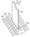
次いで、フラットケーブル62を吸着器で保持しつつ移動させ、フラットケーブル62の一端を第1プリント基板50に接続し他端を第2プリント基板52に接続する。この工程を接続工程と称する。図6は、吸着器でフラットケーブルを保持したことを示す斜視図である。吸着器102の平坦な吸着面102aを、フラットケーブル62の平坦面62cに当ててフラットケーブル62を吸着器102に吸着させる。これにより、吸着器102を用いてフラットケーブル62を自動搬送できる。
Next, the
図7は、接続工程後のフラットケーブル等を示す平面図である。事前にプリント基板50、52、54を一平面に並べておき、吸着器102による自動搬送でフラットケーブル62(電線62a)の一端を第1プリント基板50に接続し他端を第2プリント基板52に接続する。同様に、フラットケーブル64も吸着器102で自動搬送し、フラットケーブル64(電線64a)の一端を第2プリント基板52に接続し他端を第3プリント基板54に接続する。これらの接続は、例えばはんだ付けや超音波接合で実施する。
FIG. 7 is a plan view showing the flat cable and the like after the connecting step. The printed
次いで、フラットケーブル62を折り曲げて第1プリント基板50と第2プリント基板52を対向させる。また、フラットケーブル64を折り曲げて第2プリント基板52と第3プリント基板54を対向させる。この工程を折り曲げ工程と称する。折り曲げ工程を終えると、プリント基板50、52、54が相互に離間しつつ重ねられる。次いで、フラットケーブル62、64により一体化したプリント基板50、52、54をケース内に導入し、図1に示す接続を行うことで半導体装置10が完成する。
Next, the
本発明の実施の形態1に係る半導体装置10によれば、フラットケーブル62、64に平坦面が形成されているので、フラットケーブル62、64を吸着器102でピックアップし自動搬送できる。よって、製造工程におけるスループットアップを高めることができる。
According to the
平坦面62cは電線62aと略直交する方向に伸びる細長い形状で形成したため、折り曲げ工程においてこの平坦面62cを起点に折り曲げることが可能である。また、平坦面62cが形成された部分は他の部分よりは強度が弱いので折り曲げが容易になる。フラットケーブル60、64についても同様である。
Since the
本発明の実施の形態1に係る半導体装置10によれば、フラットケーブル62、64でプリント基板50、52、54間の電気的接続をとるので、プリント基板50、52、54間を接続するための「端子」は不要である。よって、そのような端子がプリント基板50、52、54上を占有することがないので、回路部品56のための実装面積を大きくできる。しかも、第1プリント基板50と半導体素子30の接続にフラットケーブル60を用いたので、この部分でも端子の使用を回避できている。
According to the
フラットケーブル60は、第1プリント基板50に端子が接続されて第1プリント基板50の実装面積を低減させることを回避するために形成されている。従って、フラットケーブル60は、導線であれば特に限定されない。例えば、フラットケーブル60としてボンディングワイヤを採用してもよい。
The
本発明は、複数の基板を重ねて配置する場合において、容易な方法で製造工程のスループットを高めつつ、基板の実装面積を大きくできるものである。従って、半導体素子の種類や半導体装置が備える基板の枚数及び機能は特に限定されない。 The present invention can increase the mounting area of a substrate while increasing the throughput of the manufacturing process by an easy method when a plurality of substrates are arranged in an overlapping manner. Accordingly, there are no particular limitations on the type of semiconductor element and the number and function of substrates included in the semiconductor device.
実施の形態2.
本発明の実施の形態2に係る半導体装置とその製造方法は、実施の形態1との一致点が多い。そのため実施の形態1との相違点を中心に説明する。図8は、本発明の実施の形態2に係る半導体装置の断面図である。この半導体装置は、中継端子150を有している。中継端子150の下部はケース70に固定されている。
Embodiment 2. FIG.
The semiconductor device and the manufacturing method thereof according to the second embodiment of the present invention have many points of coincidence with the first embodiment. Therefore, it demonstrates centering on difference with Embodiment 1. FIG. FIG. 8 is a cross-sectional view of the semiconductor device according to the second embodiment of the present invention. This semiconductor device has a
中継端子150はワイヤ152を介して半導体素子30と接続されている。中継端子150の上方にはフラットケーブル154が接続されている。フラットケーブル154の一端は第1プリント基板50に接続され、他端は中継端子150に接続されている。なお、フラットケーブル154はフラットケーブル62と同じものである。
The
実施の形態1のようにフラットケーブル60を用いて第1プリント基板50と配線パターン14を接続するのはやや複雑な作業を要し、製造工程のスループットを低下させるおそれがある。しかしながら、本発明の実施の形態2に係る半導体装置によれば、中継端子150がケース70内部で上方に長く伸びているので、フラットケーブル154の他端を容易に中継端子150に接続できる。従って実施の形態1の製造方法と比較して製造工程のスループットを高めることができる。なお、本発明の実施の形態2に係る半導体装置は、少なくとも実施の形態1と同程度の変形が可能である。
Connecting the first printed
実施の形態3.
本発明の実施の形態3に係る半導体装置とその製造方法は、実施の形態1との一致点が多い。そのため実施の形態1との相違点を中心に説明する。図9は、本発明の実施の形態3に係る半導体装置の断面図である。この半導体装置は、フラットケーブル200を有している。フラットケーブル200の一端は第1プリント基板50に接続され、他端は半導体素子30に接続されている。なお、フラットケーブル200はフラットケーブル62と同じものである。
Embodiment 3 FIG.
The semiconductor device and its manufacturing method according to the third embodiment of the present invention have many points of coincidence with the first embodiment. Therefore, it demonstrates centering on difference with Embodiment 1. FIG. FIG. 9 is a cross-sectional view of the semiconductor device according to the third embodiment of the present invention. This semiconductor device has a flat cable 200. One end of the flat cable 200 is connected to the first printed
このように、フラットケーブル200で第1プリント基板50と半導体素子30を接続すると、図1で示した配線パターン14、ワイヤ32、及び図8で示した中継端子150が不要となる。よって、半導体装置を低コスト化できる。なお、本発明の実施の形態3に係る半導体装置は、少なくとも実施の形態1と同程度の変形が可能である。
Thus, when the first printed
10 半導体装置、 12 絶縁基板、 14,16,18 配線パターン、 30 半導体素子、 32,34 ワイヤ、 50 第1プリント基板、 52 第2プリント基板、 54 第3プリント基板、 56 回路部品、 60 フラットケーブル、 60a 電線、 60b 被膜、 62 フラットケーブル、 62a 電線、 62b 被膜、 62c 平坦面、 64 フラットケーブル、 66 制御端子、 70 ケース、 74 電力端子、 100 加熱プレス装置、 102 吸着器
DESCRIPTION OF
Claims (9)
電線と、前記電線の両端を露出させつつ前記電線を覆う被膜を有し、前記電線の一端が前記第1プリント基板に接続されたフラットケーブルと、
前記電線の他端と接続された第2プリント基板と、を備え、
前記フラットケーブルは、前記第1プリント基板と前記第2プリント基板を対向させるように屈曲しており、
前記被膜の上面又は下面の一部には平坦面が形成され、前記被膜の上面と下面のうち前記平坦面が形成されていない部分は曲面であることを特徴とする半導体装置。 A first printed circuit board;
A flat cable having an electric wire and a coating covering the electric wire while exposing both ends of the electric wire, and one end of the electric wire connected to the first printed circuit board;
A second printed circuit board connected to the other end of the electric wire,
The flat cable is bent so that the first printed circuit board and the second printed circuit board are opposed to each other,
A flat surface is formed on a part of an upper surface or a lower surface of the coating, and a portion of the upper and lower surfaces of the coating where the flat surface is not formed is a curved surface .
前記フラットケーブルは、前記平坦面が形成された部分に沿って屈曲することを特徴とする請求項1に記載の半導体装置。 The flat surface Ri elongated der extending in a direction substantially orthogonal to the electric wire,
The semiconductor device according to claim 1, wherein the flat cable is bent along a portion where the flat surface is formed .
前記絶縁基板の上に形成された半導体素子と、
一端が前記半導体素子と電気的に接続され、他端が前記第1プリント基板に電気的に接続された導線を備えたことを特徴とする請求項1乃至3のいずれか1項に記載の半導体装置。 An insulating substrate;
A semiconductor element formed on the insulating substrate;
4. The semiconductor according to claim 1, further comprising a conductive wire having one end electrically connected to the semiconductor element and the other end electrically connected to the first printed circuit board. apparatus.
前記ワイヤと接続された中継端子と、を備え、
前記導線の一端は前記中継端子と接続されたことを特徴とする請求項4に記載の半導体装置。 A wire connected to the semiconductor element;
A relay terminal connected to the wire,
The semiconductor device according to claim 4, wherein one end of the conducting wire is connected to the relay terminal.
平坦な吸着面を有する吸着器の前記吸着面を前記平坦面に当てて、前記吸着器で前記フラットケーブルを保持しつつ移動させ、前記フラットケーブルの一端を第1プリント基板に接続し他端を第2プリント基板に接続する工程と、
前記フラットケーブルを折り曲げて前記第1プリント基板と前記第2プリント基板を対向させる工程と、を備えたことを特徴とする半導体装置の製造方法。 Some of the upper surface or the lower surface of the flat cable ends lower and upper surfaces brewing covering the wire while exposing the electrical wire with a coating which is curved, forming a flat surface,
The suction surface of the suction device having a flat suction surface is applied to the flat surface and moved while holding the flat cable by the suction device, and one end of the flat cable is connected to the first printed circuit board and the other end is connected. Connecting to a second printed circuit board;
And a step of bending the flat cable to make the first printed circuit board and the second printed circuit board face each other.
前記フラットケーブルを折り曲げる際は、前記平坦面が形成された部分に沿って前記フラットケーブルを折り曲げることを特徴とする請求項8に記載の半導体装置の製造方法。 9. The method of manufacturing a semiconductor device according to claim 8, wherein when the flat cable is bent, the flat cable is bent along a portion where the flat surface is formed.
Priority Applications (4)
| Application Number | Priority Date | Filing Date | Title |
|---|---|---|---|
| JP2012101297A JP5660076B2 (en) | 2012-04-26 | 2012-04-26 | Semiconductor device and manufacturing method thereof |
| US13/828,142 US9125308B2 (en) | 2012-04-26 | 2013-03-14 | Semiconductor device and method of manufacturing thereof |
| DE102013204565.4A DE102013204565B4 (en) | 2012-04-26 | 2013-03-15 | Semiconductor device and method of manufacturing the same |
| CN201310147145.XA CN103379735B (en) | 2012-04-26 | 2013-04-25 | Semiconductor device and manufacture method thereof |
Applications Claiming Priority (1)
| Application Number | Priority Date | Filing Date | Title |
|---|---|---|---|
| JP2012101297A JP5660076B2 (en) | 2012-04-26 | 2012-04-26 | Semiconductor device and manufacturing method thereof |
Publications (3)
| Publication Number | Publication Date |
|---|---|
| JP2013229489A JP2013229489A (en) | 2013-11-07 |
| JP2013229489A5 JP2013229489A5 (en) | 2014-10-09 |
| JP5660076B2 true JP5660076B2 (en) | 2015-01-28 |
Family
ID=49323389
Family Applications (1)
| Application Number | Title | Priority Date | Filing Date |
|---|---|---|---|
| JP2012101297A Active JP5660076B2 (en) | 2012-04-26 | 2012-04-26 | Semiconductor device and manufacturing method thereof |
Country Status (4)
| Country | Link |
|---|---|
| US (1) | US9125308B2 (en) |
| JP (1) | JP5660076B2 (en) |
| CN (1) | CN103379735B (en) |
| DE (1) | DE102013204565B4 (en) |
Family Cites Families (25)
| Publication number | Priority date | Publication date | Assignee | Title |
|---|---|---|---|---|
| JPS4860075U (en) * | 1971-11-12 | 1973-07-31 | ||
| JPS5340476U (en) * | 1976-09-10 | 1978-04-07 | ||
| JPS5943593A (en) | 1982-09-06 | 1984-03-10 | 富士通株式会社 | Method of producing electronic circuit module |
| DE8413336U1 (en) | 1984-05-02 | 1984-08-23 | Gossen Gmbh, 8520 Erlangen | Ribbon cable |
| JP2678327B2 (en) * | 1991-02-15 | 1997-11-17 | 住友金属鉱山株式会社 | Flexible wiring board and manufacturing method thereof |
| US5428190A (en) * | 1993-07-02 | 1995-06-27 | Sheldahl, Inc. | Rigid-flex board with anisotropic interconnect and method of manufacture |
| JP3286104B2 (en) * | 1995-01-24 | 2002-05-27 | ヒロセ電機株式会社 | Coaxial semi-rigid cable assembly with holder |
| JP3430192B2 (en) * | 1996-11-12 | 2003-07-28 | 株式会社日立産機システム | Inverter device |
| JPH10209594A (en) * | 1997-01-17 | 1998-08-07 | Fuji Photo Optical Co Ltd | Connection structure of flexible printed circuit board and rigid printed circuit board |
| KR100422089B1 (en) * | 1999-04-22 | 2004-03-11 | 롬 가부시키가이샤 | Circuit board, battery pack, and method of manufacturing circuit board |
| JP3667176B2 (en) * | 1999-11-12 | 2005-07-06 | 平河ヒューテック株式会社 | Flat cable and manufacturing method thereof |
| JP4667652B2 (en) * | 2001-06-12 | 2011-04-13 | ローム株式会社 | Battery pack and manufacturing method thereof |
| JP4330294B2 (en) | 2001-08-10 | 2009-09-16 | 三菱電機株式会社 | Power semiconductor device |
| JP2003100156A (en) | 2001-09-26 | 2003-04-04 | Canon Inc | Cable and electronic apparatus |
| JP2004297972A (en) * | 2003-03-28 | 2004-10-21 | Toyota Industries Corp | Semiconductor device |
| JP4265394B2 (en) * | 2003-12-17 | 2009-05-20 | 株式会社日立製作所 | Power converter |
| US7148428B2 (en) | 2004-09-27 | 2006-12-12 | Intel Corporation | Flexible cable for high-speed interconnect |
| JP4673211B2 (en) * | 2005-12-27 | 2011-04-20 | 日立オートモティブシステムズ株式会社 | Power converter |
| JP4827971B2 (en) | 2007-09-21 | 2011-11-30 | 三菱電機株式会社 | Flexible wiring board fixing structure |
| JP2010105640A (en) | 2008-10-31 | 2010-05-13 | Nsk Ltd | Electric power steering device |
| JP2010165914A (en) | 2009-01-16 | 2010-07-29 | Toshiba Carrier Corp | Inverter device and method of manufacturing inverter device |
| JP5153706B2 (en) | 2009-03-26 | 2013-02-27 | 京セラ株式会社 | Hybrid integrated circuit device for ECU |
| JP5375408B2 (en) * | 2009-07-24 | 2013-12-25 | 住友電気工業株式会社 | Coaxial wire harness |
| WO2012039114A1 (en) * | 2010-09-24 | 2012-03-29 | オンセミコンダクター・トレーディング・リミテッド | Circuit device |
| JP5579576B2 (en) | 2010-11-08 | 2014-08-27 | サンドビック株式会社 | Endless belt manufacturing method and mounting method |
-
2012
- 2012-04-26 JP JP2012101297A patent/JP5660076B2/en active Active
-
2013
- 2013-03-14 US US13/828,142 patent/US9125308B2/en active Active
- 2013-03-15 DE DE102013204565.4A patent/DE102013204565B4/en active Active
- 2013-04-25 CN CN201310147145.XA patent/CN103379735B/en active Active
Also Published As
| Publication number | Publication date |
|---|---|
| DE102013204565A1 (en) | 2013-10-31 |
| CN103379735A (en) | 2013-10-30 |
| DE102013204565B4 (en) | 2023-04-20 |
| US9125308B2 (en) | 2015-09-01 |
| JP2013229489A (en) | 2013-11-07 |
| CN103379735B (en) | 2016-06-08 |
| US20130286622A1 (en) | 2013-10-31 |
Similar Documents
| Publication | Publication Date | Title |
|---|---|---|
| JP6305302B2 (en) | Semiconductor device and manufacturing method thereof | |
| KR100935854B1 (en) | Microelectronic assembly with impedance controlled wirebond and reference wirebond | |
| KR20090009737A (en) | Semiconductor apparatus and manufacturing method thereof | |
| US7071543B2 (en) | Semiconductor device and manufacturing method thereof | |
| JP2010027996A (en) | High-frequency module, and method of manufacturing the same | |
| US20190254164A1 (en) | Circuit board, method of manufacturing circuit board, and electronic device | |
| KR102047775B1 (en) | Chip packaging structure and related inner lead bonding method | |
| JP5415525B2 (en) | Electrical bonding connection structure | |
| JP2011151103A (en) | Electronic component interconnecting structure and connecting method | |
| JP2012222124A (en) | Capacitor with insulating coating and manufacturing method therefor | |
| JP5660076B2 (en) | Semiconductor device and manufacturing method thereof | |
| JP2011159933A (en) | Power semiconductor device, and method of manufacturing same | |
| JP2001102712A (en) | Wiring board with connector and manufacturing method therefor | |
| JP6312527B2 (en) | Electronic component mounting structure with heat sink | |
| KR102004777B1 (en) | Method for manufacturing package, and package using the same | |
| JP5198173B2 (en) | Terminal mounting structure with busbar | |
| JP5835166B2 (en) | Semiconductor device and method for manufacturing semiconductor device | |
| JP5229200B2 (en) | Manufacturing method of semiconductor device | |
| US20150016069A1 (en) | Printed circuit board | |
| TWI571995B (en) | Apparatus having multi-connect lead, chip package having multi-connect lead and method for conserving external pins of lead-frame substructure | |
| JP4571012B2 (en) | Crystal unit with pedestal | |
| US20130069217A1 (en) | Semiconductor device and electrode terminal | |
| JP4954778B2 (en) | Three-dimensional electronic circuit device and connecting member | |
| TW201724430A (en) | Semiconductor device, lead frame, and method of manufacturing lead frame | |
| CN109287128A (en) | The manufacturing method of chip module |
Legal Events
| Date | Code | Title | Description |
|---|---|---|---|
| A521 | Request for written amendment filed |
Free format text: JAPANESE INTERMEDIATE CODE: A523 Effective date: 20140516 |
|
| A621 | Written request for application examination |
Free format text: JAPANESE INTERMEDIATE CODE: A621 Effective date: 20140516 |
|
| A521 | Request for written amendment filed |
Free format text: JAPANESE INTERMEDIATE CODE: A523 Effective date: 20140821 |
|
| A977 | Report on retrieval |
Free format text: JAPANESE INTERMEDIATE CODE: A971007 Effective date: 20140827 |
|
| A131 | Notification of reasons for refusal |
Free format text: JAPANESE INTERMEDIATE CODE: A131 Effective date: 20140924 |
|
| A521 | Request for written amendment filed |
Free format text: JAPANESE INTERMEDIATE CODE: A523 Effective date: 20141007 |
|
| TRDD | Decision of grant or rejection written | ||
| A01 | Written decision to grant a patent or to grant a registration (utility model) |
Free format text: JAPANESE INTERMEDIATE CODE: A01 Effective date: 20141104 |
|
| A61 | First payment of annual fees (during grant procedure) |
Free format text: JAPANESE INTERMEDIATE CODE: A61 Effective date: 20141117 |
|
| R150 | Certificate of patent or registration of utility model |
Ref document number: 5660076 Country of ref document: JP Free format text: JAPANESE INTERMEDIATE CODE: R150 |
|
| R250 | Receipt of annual fees |
Free format text: JAPANESE INTERMEDIATE CODE: R250 |
|
| R250 | Receipt of annual fees |
Free format text: JAPANESE INTERMEDIATE CODE: R250 |
|
| R250 | Receipt of annual fees |
Free format text: JAPANESE INTERMEDIATE CODE: R250 |
|
| R250 | Receipt of annual fees |
Free format text: JAPANESE INTERMEDIATE CODE: R250 |
|
| R250 | Receipt of annual fees |
Free format text: JAPANESE INTERMEDIATE CODE: R250 |
|
| R250 | Receipt of annual fees |
Free format text: JAPANESE INTERMEDIATE CODE: R250 |
|
| R250 | Receipt of annual fees |
Free format text: JAPANESE INTERMEDIATE CODE: R250 |