JP5653109B2 - Semiconductor device - Google Patents
Semiconductor device Download PDFInfo
- Publication number
- JP5653109B2 JP5653109B2 JP2010167418A JP2010167418A JP5653109B2 JP 5653109 B2 JP5653109 B2 JP 5653109B2 JP 2010167418 A JP2010167418 A JP 2010167418A JP 2010167418 A JP2010167418 A JP 2010167418A JP 5653109 B2 JP5653109 B2 JP 5653109B2
- Authority
- JP
- Japan
- Prior art keywords
- layer
- semiconductor device
- conductive layer
- electrode
- channel layer
- Prior art date
- Legal status (The legal status is an assumption and is not a legal conclusion. Google has not performed a legal analysis and makes no representation as to the accuracy of the status listed.)
- Active
Links
Images
Landscapes
- Junction Field-Effect Transistors (AREA)
Description
本発明は半導体装置に関し、特に窒化物半導体層を有する半導体装置に関する。 The present invention relates to a semiconductor device, and more particularly to a semiconductor device having a nitride semiconductor layer.
FET(Field Effect Transistor:電界効果型トランジスタ)等の半導体装置では、窒化物半導体層上に、ソース電極、ドレイン電極、及びゲート電極を形成する。特許文献1には、基板にイオン注入をすることで、リーク電流を抑制する発明が開示されている。 In a semiconductor device such as an FET (Field Effect Transistor), a source electrode, a drain electrode, and a gate electrode are formed on a nitride semiconductor layer. Patent Document 1 discloses an invention that suppresses leakage current by ion implantation into a substrate.
従来の技術では、水分の浸入によって、半導体装置の信頼性が低下する可能性があった。本発明は上記課題に鑑み、信頼性を向上させることが可能な半導体装置を提供することを目的とする。 In the conventional technology, there is a possibility that the reliability of the semiconductor device is lowered due to the ingress of moisture. In view of the above problems, an object of the present invention is to provide a semiconductor device capable of improving reliability.
本発明は、基板上に設けられたGaNからなるチャネル層と、前記チャネル層上の窒化物半導体層の上に設けられたソース電極、ドレイン電極及びゲート電極と、前記基板と前記チャネル層との間に設けられ、Si濃度が5×1015cm−3以上、1×1017cm−3以下である、n型GaNからなる導電層と、を具備し、前記導電層には、前記ドレイン電極に印加される電圧が20V以上において、前記ゲート電極の幅1mmあたり、10μA以上100μA以下のリーク電流が流れる半導体装置である。本発明によれば、半導体装置の信頼性を向上させることが可能となる。また、高電圧が印加される場合においても、半導体装置の信頼性を向上させることが可能となる。
The present invention includes a channel layer made of GaN provided on a substrate, a source electrode, a drain electrode and a gate electrode provided on a nitride semiconductor layer on the channel layer, and the substrate and the channel layer. A conductive layer made of n-type GaN with a Si concentration of 5 × 10 15 cm −3 or more and 1 × 10 17 cm −3 or less provided between the drain electrode and the drain electrode. In the semiconductor device, a leak current of 10 μA or more and 100 μA or less flows through 1 mm of the width of the gate electrode when the voltage applied to the gate electrode is 20 V or more . According to the present invention, it is possible to improve the reliability of a semiconductor device . In addition, even when a high voltage is applied, the reliability of the semiconductor device can be improved.
上記構成において、前記基板と前記チャネル層との間に設けられたバッファ層を備え、前記導電層は、前記バッファ層の上面と前記チャネル層の上面との中間位置から、前記バッファ層の上面までの領域に設けられてなる構成とすることができる。この構成によれば、半導体装置の特性の悪化を抑制し、かつ耐湿性を改善させることができる。 In the above structure, a buffer layer is provided between the substrate and the channel layer, and the conductive layer extends from an intermediate position between the upper surface of the buffer layer and the upper surface of the channel layer to the upper surface of the buffer layer. It can be set as the structure formed in this area | region. According to this configuration, it is possible to suppress the deterioration of the characteristics of the semiconductor device and improve the moisture resistance.
上記構成において、前記導電層の前記Si濃度は、1×1016cm−3以上、1×1017cm−3以下である構成とすることができる。この構成によれば、半導体装置の信頼性を向上させることが可能となる。 In the above structure, the Si concentration of the conductive layer may be 1 × 10 16 cm −3 or more and 1 × 10 17 cm −3 or less. According to this configuration, the reliability of the semiconductor device can be improved.
本発明によれば、信頼性を向上させることが可能な半導体装置を提供することができる。 According to the present invention, a semiconductor device capable of improving reliability can be provided.
実施例の説明の前に、まず半導体装置の信頼性が低下する原因について説明する。半導体装置のうち、FETでは、例えばi型GaN(窒化ガリウム)からなるチャネル層上にソース電極、ドレイン電極及びゲート電極を形成する。各電極は、例えばAu等の金属からなる。 Prior to the description of the embodiments, the cause of the decrease in the reliability of the semiconductor device will be described first. In the FET of the semiconductor device, a source electrode, a drain electrode, and a gate electrode are formed on a channel layer made of, for example, i-type GaN (gallium nitride). Each electrode is made of a metal such as Au.
半導体装置に水分が浸入した場合、電極を形成するAuが水分に溶け出し、イオン化することがある。この場合に、電極に電圧を印加すると、一方の電極から溶け出したAuイオンが移動し、別の電極で還元され析出する、いわゆるイオンマイグレーション現象が発生することがある。イオンマイグレーション現象について検証するため、ドレイン電圧Vd=50V,ゲート電圧Vg=−3〜−5Vのピンチオフ状態の半導体装置を、温度130℃、湿度85%の環境下に配置する加速試験を行った。その結果、ドレイン電極から溶け出したAuが、ソース電極及びゲート電極で析出した。イオンマイグレーション現象が発生すると、半導体装置が破壊される等、半導体装置の信頼性が低下する。特に、窒化物半導体を用いる半導体装置の場合、高電圧が印加されるため、イオンマイグレーション現象の影響が大きくなる。 When moisture enters the semiconductor device, Au forming the electrode may dissolve into the moisture and be ionized. In this case, when a voltage is applied to the electrode, a so-called ion migration phenomenon may occur in which Au ions dissolved from one electrode move and are reduced and precipitated by another electrode. In order to verify the ion migration phenomenon, an acceleration test was performed in which a pinch-off semiconductor device having a drain voltage Vd = 50 V and a gate voltage Vg = −3 to −5 V was placed in an environment of a temperature of 130 ° C. and a humidity of 85%. As a result, Au dissolved from the drain electrode was deposited at the source electrode and the gate electrode. When the ion migration phenomenon occurs, the reliability of the semiconductor device decreases, for example, the semiconductor device is destroyed. In particular, in the case of a semiconductor device using a nitride semiconductor, since a high voltage is applied, the influence of the ion migration phenomenon becomes large.
水分の浸入を抑制するために、透水性の低い保護膜が用いられることがある。しかしこの場合、保護膜の質、膜厚、電極等との密着性等を管理することが求められる。従って、半導体装置の構成や製造工程が複雑となることがあった。また、保護膜の質等にバラつきがあると、多数の半導体装置の中で耐湿性にバラつきが発生することがあった。 A protective film with low water permeability may be used to suppress moisture intrusion. However, in this case, it is required to manage the quality of the protective film, the film thickness, the adhesion with the electrodes and the like. Therefore, the configuration and manufacturing process of the semiconductor device may be complicated. In addition, when the quality of the protective film varies, the moisture resistance may vary among many semiconductor devices.
本発明の発明者は、半導体装置の動作時に流れるドレイン電流と比較して微小なリーク電流が、ソース−ドレイン間又はソース−ゲート間に流れることで、半導体装置の耐湿性が大きく改善することを見出した。本発明は、この知見に基づくものである。 The inventor of the present invention shows that the moisture resistance of the semiconductor device is greatly improved by flowing a small leak current between the source and drain or between the source and gate as compared with the drain current flowing when the semiconductor device operates. I found it. The present invention is based on this finding.
次に図面を用いて、本発明の実施例について説明する。図1は実施例1に係る半導体装置を例示する断面図である。 Next, embodiments of the present invention will be described with reference to the drawings. FIG. 1 is a cross-sectional view illustrating a semiconductor device according to the first embodiment.
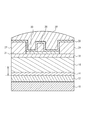
図1に示すように、実施例1に係る半導体装置は、基板10、バッファ層12、導電層14、チャネル層16、電子供給層18、キャップ層20、ソース電極22、ドレイン電極24、ゲート電極26、SiN層28、及びポリイミド層30を備える。下から順に、基板10、バッファ層12、チャネル層16、電子供給層18、及びキャップ層20が積層されている。導電層14は、チャネル層16内に設けられている。バッファ層12からキャップ層20までの各層は、例えばMOCVD法(Metal Organic Chemical Vapor Deposition:有機金属気相成長法)により形成される。
As shown in FIG. 1, the semiconductor device according to Example 1 includes a
キャップ層20にはリセス21が形成され、リセス21に、電子供給層18と接触するように、ソース電極22及びドレイン電極24が形成されている。また、キャップ層20上であって、ソース電極22及びドレイン電極24との間にゲート電極26が設けられている。つまり、ソース電極22、ドレイン電極24及びゲート電極26は、チャネル層16上の窒化物半導体層の上(電子供給層18上及びキャップ層20上)に設けられている。ソース電極22、ドレイン電極24、及びゲート電極26上にはSiN層28が設けられ、SiN層28上にはポリイミド層30が設けられている。
A
基板10は、例えばSiC(炭化シリコン)、Siやサファイア等からなる。バッファ層12は、例えば厚さ300nmのAlN(窒化アルミニウム)からなる。チャネル層16は、例えば厚さ1000nmのi型GaNからなる。電子供給層18は、例えば厚さ20nmのAlGaN(窒化アルミニウムガリウム)からなる。キャップ層20は、例えば厚さ5nmのn型GaNからなる。ソース電極22及びドレイン電極24は、例えば下から順にTi/Al/Au又はTa/Al/Au等の金属を積層してなる。Ti/Alの層はオーミック電極を形成し、Au層は配線を形成する。Au層は、大きな電流を流すため、オーミック電極よりも大きく形成される。ゲート電極26は、例えば下から順にNi/Auを積層してなる。SiN層28及びポリイミド層30は、耐湿性の保護膜として機能する。
The
導電層14は、チャネル層16内であって、チャネル層16の下側の領域に設けられている。図中では導電層14はチャネル層16の最下層(バッファ層12の上面)に設けられているが、バッファ層12の上面とチャネル層16の上面との中間位置からバッファ層12の上面までの領域内に設けられていればよい(図中の矢印参照)。導電層14の厚さは例えば100〜300nmである。導電層14は、不純物として例えばSiを含む。Siの濃度は例えば5×1015cm−3以上、1×1017cm−3以下である。次に導電層14により半導体装置の耐湿性が改善する原因について説明する。
The
ドレイン電圧Vdが20V以上の状態では、導電層14に、ゲート電極26の幅(ゲート幅)1mmあたり例えば10〜100μA程度のリーク電流が流れる。電流は、半導体装置の動作時にも、非動作時にも導電層14に流れる。導電層14にリーク電流が流れることにより、電極間を移動するAuイオンが少なくなり、イオンマイグレーション現象が抑制されると考えられる。又は、導電層14は、リーク電流が流れることにより発熱する。導電層14の発熱により、浸入した水分が蒸発し、Auが溶け出すことが抑制されると考えられる。
In the state where the drain voltage Vd is 20 V or more, a leak current of, for example, about 10 to 100 μA flows through the
実施例1によれば、チャネル層16内の下側の領域に、n型GaNからなる導電層14が設けられているため、イオンマイグレーション現象を抑制することができる。すなわち半導体装置の耐湿性が改善し、信頼性を向上させることが可能となる。
According to Example 1, since the
導電層14は、例えばMOCVD法によりエピタキシャル成長されるため、簡単な工程で、安定して形成される。これにより、構成及び工程の複雑化を回避し、かつ半導体装置の信頼性を向上させることができる。特に、i型GaNのような窒化物半導体では高電圧が印加されるため、イオンマイグレーション現象が発生しやすい。実施例1によれば、i型GaNをチャネル層16とした場合でも、イオンマイグレーション現象を抑制することができる。例えばドレイン電圧Vdが20V以上の場合、さらにドレイン電圧が50V以上の場合でも、半導体装置の耐湿性を改善させることができる。
Since the
導電層14がチャネル層16の電子供給層18に近い領域に設けられている場合、半導体装置の特性が変動する恐れがある。このため、導電層14は、バッファ層12の上面とチャネル層16の上面との中間位置からバッファ層12の上面までの領域内に設けられていればよい。例えばチャネル層16の厚さが1000nmである場合、チャネル層16の下から500nm以内の領域に導電層14が設けられることが好ましい。
When the
例えばドレイン電圧Vdが20V以上で、半導体装置の動作時のドレイン電流がゲート幅1mmあたり700〜800mAである場合、導電層14に流れるリーク電流は10〜100μA程度である。つまり、導電層14に流れるリーク電流は、半導体装置の動作時に流れるドレイン電流よりも3桁〜4桁程度小さい。このため、導電層14に流れるリーク電流による、半導体装置の特性の変動は極めて小さい。これにより、半導体装置の特性の悪化を抑制し、かつ耐湿性を改善させることができる。半導体装置の特性の変動を抑制するためには、導電層14に流れるリーク電流は、ドレイン電流より4桁小さいことが好ましい。
For example, when the drain voltage Vd is 20 V or more and the drain current during operation of the semiconductor device is 700 to 800 mA per 1 mm of gate width, the leakage current flowing through the
導電層14に含まれる不純物であるSiの濃度が高すぎると、導電層14に流れるリーク電流が大きくなり、半導体装置の特性が悪化する。またSiの濃度が低すぎると、リーク電流が小さくなり体質性の改善が十分に行われない。ドレイン電流よりも3桁〜4桁小さいリーク電流を導電層14に流すためには、導電層14に含まれる不純物であるSiの濃度は5×1015cm−3以上、1×1017cm−3以下、厚さは200〜300nmであることが好ましい。さらに好ましくは、Siの濃度が、1×1016cm−3以上、1×1017cm−3以下であることが好ましい。また、導電層14に含まれる不純物はSiに限定されず、n型GaNを形成する不純物であればよい。つまり導電層14は、ドレイン電流よりも3桁〜4桁小さい電流が流れるn型GaN層であればよい。導電層14は、ドレイン電圧が20V以上の場合に、ドレイン電流よりも3桁〜4桁小さいリーク電流が流れるような、厚さや不純物濃度を有する導電層であることが好ましい。さらに、50V以上のような高電圧の場合でも、導電層14にはドレイン電流よりも3桁〜4桁小さい電流が流れることが好ましい。
If the concentration of Si, which is an impurity contained in the
キャップ層20は設けられていなくてもよい。キャップ層20が設けられていない場合、ソース電極22、ドレイン電極24及びゲート電極26は、電子供給層18上に設けられる。つまり、ソース電極22、ドレイン電極24及びゲート電極26は、i型GaNからなるチャネル層16の上側に設けられる。
The
なお、バッファ層12、電子供給層18及びキャップ層20は、GaN、AlN、AlGaN以外の窒化物半導体としてもよい。窒化物半導体は、窒素を含む半導体であり、GaNやAlGaN、AlN以外に、例えばInN(窒化インジウム)、InGaN(窒化インジウムガリウム)、InAlN(窒化インジウムアルミニウム)、及びAlInGaN(窒化アルミニウムインジウムガリウム)等がある。
The
以上、本発明の実施例について詳述したが、本発明はかかる特定の実施例に限定されるものではなく、特許請求の範囲に記載された本発明の要旨の範囲内において、種々の変形・変更が可能である。 Although the embodiments of the present invention have been described in detail above, the present invention is not limited to such specific embodiments, and various modifications and changes can be made within the scope of the gist of the present invention described in the claims. It can be changed.
基板 10
バッファ層 12
導電層 14
チャネル層 16
電子供給層 18
キャップ層 20
ソース電極 22
ドレイン電極 24
ゲート電極 26
SiN層 28
ポリイミド層 30
Claims (3)
前記チャネル層上の窒化物半導体層の上に設けられたソース電極、ドレイン電極及びゲート電極と、
前記基板と前記チャネル層との間に設けられ、Si濃度が5×1015cm−3以上、1×1017cm−3以下である、n型GaNからなる導電層と、を具備し、
前記導電層には、前記ドレイン電極に印加される電圧が20V以上において、前記ゲート電極の幅1mmあたり、10μA以上100μA以下のリーク電流が流れることを特徴とする半導体装置。 A channel layer made of GaN provided on a substrate;
A source electrode, a drain electrode and a gate electrode provided on the nitride semiconductor layer on the channel layer;
A conductive layer made of n-type GaN provided between the substrate and the channel layer and having a Si concentration of 5 × 10 15 cm −3 or more and 1 × 10 17 cm −3 or less ,
A semiconductor device , wherein a leak current of 10 μA or more and 100 μA or less flows through the conductive layer per 1 mm width of the gate electrode when a voltage applied to the drain electrode is 20 V or more .
前記導電層は、前記バッファ層の上面と前記チャネル層の上面との中間位置から、前記バッファ層の上面までの領域に設けられてなることを特徴とする請求項1記載の半導体装置。 A buffer layer provided between the substrate and the channel layer;
2. The semiconductor device according to claim 1, wherein the conductive layer is provided in a region from an intermediate position between an upper surface of the buffer layer and an upper surface of the channel layer to an upper surface of the buffer layer.
Priority Applications (1)
| Application Number | Priority Date | Filing Date | Title |
|---|---|---|---|
| JP2010167418A JP5653109B2 (en) | 2010-07-26 | 2010-07-26 | Semiconductor device |
Applications Claiming Priority (1)
| Application Number | Priority Date | Filing Date | Title |
|---|---|---|---|
| JP2010167418A JP5653109B2 (en) | 2010-07-26 | 2010-07-26 | Semiconductor device |
Publications (2)
| Publication Number | Publication Date |
|---|---|
| JP2012028644A JP2012028644A (en) | 2012-02-09 |
| JP5653109B2 true JP5653109B2 (en) | 2015-01-14 |
Family
ID=45781206
Family Applications (1)
| Application Number | Title | Priority Date | Filing Date |
|---|---|---|---|
| JP2010167418A Active JP5653109B2 (en) | 2010-07-26 | 2010-07-26 | Semiconductor device |
Country Status (1)
| Country | Link |
|---|---|
| JP (1) | JP5653109B2 (en) |
Families Citing this family (1)
| Publication number | Priority date | Publication date | Assignee | Title |
|---|---|---|---|---|
| JP6197344B2 (en) * | 2013-04-18 | 2017-09-20 | 住友電気工業株式会社 | Semiconductor device |
Family Cites Families (5)
| Publication number | Priority date | Publication date | Assignee | Title |
|---|---|---|---|---|
| SE9500013D0 (en) * | 1995-01-03 | 1995-01-03 | Abb Research Ltd | Semiconductor device having a passivation layer |
| JP4041660B2 (en) * | 2001-05-31 | 2008-01-30 | ユーディナデバイス株式会社 | Semiconductor device and manufacturing method thereof |
| JP4691060B2 (en) * | 2007-03-23 | 2011-06-01 | 古河電気工業株式会社 | GaN-based semiconductor devices |
| JP4584293B2 (en) * | 2007-08-31 | 2010-11-17 | 富士通株式会社 | Nitride semiconductor device, Doherty amplifier, drain voltage control amplifier |
| EP2498293B1 (en) * | 2009-11-06 | 2018-08-01 | NGK Insulators, Ltd. | Epitaxial substrate for semiconductor element and method for producing epitaxial substrate for semiconductor element |
-
2010
- 2010-07-26 JP JP2010167418A patent/JP5653109B2/en active Active
Also Published As
| Publication number | Publication date |
|---|---|
| JP2012028644A (en) | 2012-02-09 |
Similar Documents
| Publication | Publication Date | Title |
|---|---|---|
| CN102365763B (en) | Dopant diffusion modulation in GaN buffer layers | |
| JP6066933B2 (en) | Electrode structure of semiconductor devices | |
| CN103178107B (en) | There is the high electron mobility transistor structure of the breakdown voltage property of improvement | |
| US9231093B2 (en) | High electron mobility transistor and method of manufacturing the same | |
| TWI512993B (en) | Transistor and its forming method and semiconductor component | |
| US8912572B2 (en) | High electron mobility transistor and method of manufacturing the same | |
| JP5799604B2 (en) | Semiconductor device | |
| CN102623498A (en) | Semiconductor device | |
| JP6640687B2 (en) | Semiconductor device | |
| CN111883588A (en) | Sidewall passivation for HEMT devices | |
| US20150263155A1 (en) | Semiconductor device | |
| KR20230000718A (en) | High electron mobility transistor and method for manufacturing the same | |
| CN111524958B (en) | High electron mobility transistor | |
| US9484429B2 (en) | High electron mobility transistor (HEMT) capable of absorbing a stored hole more efficiently and method for manufacturing the same | |
| US20160013305A1 (en) | Nitride semiconductor device and method for manufacturing nitride semiconductor device | |
| JP5870574B2 (en) | Semiconductor device and manufacturing method of semiconductor device | |
| JP2010206125A (en) | Gallium nitride-based high electron mobility transistor | |
| JP5420157B2 (en) | Manufacturing method of semiconductor device | |
| KR20190112523A (en) | Heterostructure Field Effect Transistor and production method thereof | |
| US20160079371A1 (en) | Semiconductor device | |
| JP2008078526A (en) | Nitride semiconductor device and its manufacturing method | |
| JP5672734B2 (en) | Semiconductor device and manufacturing method thereof | |
| JP2019047055A (en) | Transistor | |
| JP2008010526A (en) | Nitride semiconductor device, and its manufacturing method | |
| JP2012033689A (en) | Manufacturing method of semiconductor device |
Legal Events
| Date | Code | Title | Description |
|---|---|---|---|
| A621 | Written request for application examination |
Free format text: JAPANESE INTERMEDIATE CODE: A621 Effective date: 20130711 |
|
| A977 | Report on retrieval |
Free format text: JAPANESE INTERMEDIATE CODE: A971007 Effective date: 20140829 |
|
| A131 | Notification of reasons for refusal |
Free format text: JAPANESE INTERMEDIATE CODE: A131 Effective date: 20140902 |
|
| A521 | Request for written amendment filed |
Free format text: JAPANESE INTERMEDIATE CODE: A523 Effective date: 20141023 |
|
| TRDD | Decision of grant or rejection written | ||
| A01 | Written decision to grant a patent or to grant a registration (utility model) |
Free format text: JAPANESE INTERMEDIATE CODE: A01 Effective date: 20141118 |
|
| A61 | First payment of annual fees (during grant procedure) |
Free format text: JAPANESE INTERMEDIATE CODE: A61 Effective date: 20141118 |
|
| R150 | Certificate of patent or registration of utility model |
Ref document number: 5653109 Country of ref document: JP Free format text: JAPANESE INTERMEDIATE CODE: R150 |
|
| R250 | Receipt of annual fees |
Free format text: JAPANESE INTERMEDIATE CODE: R250 |
|
| R250 | Receipt of annual fees |
Free format text: JAPANESE INTERMEDIATE CODE: R250 |
|
| R250 | Receipt of annual fees |
Free format text: JAPANESE INTERMEDIATE CODE: R250 |
|
| R250 | Receipt of annual fees |
Free format text: JAPANESE INTERMEDIATE CODE: R250 |