JP5652731B2 - Controller for primary side controlled power converter, integrated circuit for power converter, power converter, method for adjusting bias winding voltage of power supply, and integrated circuit controller for power converter - Google Patents
Controller for primary side controlled power converter, integrated circuit for power converter, power converter, method for adjusting bias winding voltage of power supply, and integrated circuit controller for power converter Download PDFInfo
- Publication number
- JP5652731B2 JP5652731B2 JP2010013764A JP2010013764A JP5652731B2 JP 5652731 B2 JP5652731 B2 JP 5652731B2 JP 2010013764 A JP2010013764 A JP 2010013764A JP 2010013764 A JP2010013764 A JP 2010013764A JP 5652731 B2 JP5652731 B2 JP 5652731B2
- Authority
- JP
- Japan
- Prior art keywords
- voltage
- output
- controller
- power converter
- circuit
- Prior art date
- Legal status (The legal status is an assumption and is not a legal conclusion. Google has not performed a legal analysis and makes no representation as to the accuracy of the status listed.)
- Expired - Fee Related
Links
Images


Classifications
-
- H—ELECTRICITY
- H02—GENERATION; CONVERSION OR DISTRIBUTION OF ELECTRIC POWER
- H02M—APPARATUS FOR CONVERSION BETWEEN AC AND AC, BETWEEN AC AND DC, OR BETWEEN DC AND DC, AND FOR USE WITH MAINS OR SIMILAR POWER SUPPLY SYSTEMS; CONVERSION OF DC OR AC INPUT POWER INTO SURGE OUTPUT POWER; CONTROL OR REGULATION THEREOF
- H02M3/00—Conversion of dc power input into dc power output
- H02M3/22—Conversion of dc power input into dc power output with intermediate conversion into ac
- H02M3/24—Conversion of dc power input into dc power output with intermediate conversion into ac by static converters
- H02M3/28—Conversion of dc power input into dc power output with intermediate conversion into ac by static converters using discharge tubes with control electrode or semiconductor devices with control electrode to produce the intermediate ac
- H02M3/325—Conversion of dc power input into dc power output with intermediate conversion into ac by static converters using discharge tubes with control electrode or semiconductor devices with control electrode to produce the intermediate ac using devices of a triode or a transistor type requiring continuous application of a control signal
- H02M3/335—Conversion of dc power input into dc power output with intermediate conversion into ac by static converters using discharge tubes with control electrode or semiconductor devices with control electrode to produce the intermediate ac using devices of a triode or a transistor type requiring continuous application of a control signal using semiconductor devices only
- H02M3/33507—Conversion of dc power input into dc power output with intermediate conversion into ac by static converters using discharge tubes with control electrode or semiconductor devices with control electrode to produce the intermediate ac using devices of a triode or a transistor type requiring continuous application of a control signal using semiconductor devices only with automatic control of the output voltage or current, e.g. flyback converters
- H02M3/33523—Conversion of dc power input into dc power output with intermediate conversion into ac by static converters using discharge tubes with control electrode or semiconductor devices with control electrode to produce the intermediate ac using devices of a triode or a transistor type requiring continuous application of a control signal using semiconductor devices only with automatic control of the output voltage or current, e.g. flyback converters with galvanic isolation between input and output of both the power stage and the feedback loop
-
- H—ELECTRICITY
- H02—GENERATION; CONVERSION OR DISTRIBUTION OF ELECTRIC POWER
- H02M—APPARATUS FOR CONVERSION BETWEEN AC AND AC, BETWEEN AC AND DC, OR BETWEEN DC AND DC, AND FOR USE WITH MAINS OR SIMILAR POWER SUPPLY SYSTEMS; CONVERSION OF DC OR AC INPUT POWER INTO SURGE OUTPUT POWER; CONTROL OR REGULATION THEREOF
- H02M1/00—Details of apparatus for conversion
- H02M1/0003—Details of control, feedback or regulation circuits
- H02M1/0025—Arrangements for modifying reference values, feedback values or error values in the control loop of a converter
Landscapes
- Engineering & Computer Science (AREA)
- Power Engineering (AREA)
- Dc-Dc Converters (AREA)
- Inverter Devices (AREA)
Description
背景情報
開示の分野
本発明は一般にパワーコンバータに関し、より具体的には、軽負荷/無負荷条件での出力電圧調整の向上に関する。
Background information
FIELD OF THE DISCLOSURE The present invention relates generally to power converters, and more particularly to improving output voltage regulation under light / no load conditions.
背景
携帯電話、携帯情報端末(personal digital assistant:PDA)、ラップトップなどの多くの電気装置には、直流電源によって電力が供給される。電力は一般に高圧交流電力として壁コンセントを介して供給されるため、この高圧交流電力を多くの電気装置に使用可能な直流電力に変換するためのパワーコンバータなどの装置が必要である。動作時、パワーコンバータはコントローラを用いて、一般に負荷と称され得る電気装置に供給されるエネルギを調整し得る。一例では、コントローラは、出力電圧のフィードバック情報に応じて電力スイッチをオンとオフに切換えることによってエネルギパルスの伝達を制御して、パワーコンバータの出力における出力電圧を調整し続け得る。
Background Many electrical devices such as cellular phones, personal digital assistants (PDAs), laptops, etc. are powered by a DC power source. Since electric power is generally supplied as high-voltage AC power through a wall outlet, a device such as a power converter is required to convert this high-voltage AC power into DC power that can be used in many electrical devices. In operation, the power converter can use a controller to regulate the energy supplied to an electrical device, which can be commonly referred to as a load. In one example, the controller may continue to regulate the output voltage at the output of the power converter by controlling the transmission of energy pulses by switching the power switch on and off in response to output voltage feedback information.
あるアプリケーションでは、パワーコンバータは、パワーコンバータの入力側を出力側から分離するためのエネルギ伝達素子を含み得る。より具体的には、エネルギ伝達素子は、パワーコンバータの入力と出力との間に直流が流れるのを防止し、かつ一定の安全規則のために要求される、ガルバニック絶縁を提供し得る。エネルギ伝達素子の一般的な例は結合インダクタであり、入力側の入力巻線が受けた電気エネルギが磁気エネルギとして蓄えられ、パワーコンバータの出力側の出力巻線の両端で再び電気エネルギに変換される。 In some applications, the power converter may include an energy transfer element for separating the input side of the power converter from the output side. More specifically, the energy transfer element may prevent direct current from flowing between the input and output of the power converter and provide galvanic isolation as required for certain safety regulations. A common example of an energy transfer element is a coupled inductor, where the electrical energy received by the input winding on the input side is stored as magnetic energy and converted back to electrical energy at both ends of the output winding on the output side of the power converter. The
あるパワーコンバータの設計においては、出力電圧を指定の電圧範囲内に調整することが必要であり得る。これを達成するため、パワーコンバータの中には、「一次フィードバック」を用いてパワーコンバータの入力側から出力電圧を間接的に検知できるようにして、出力電圧を指定の範囲内に調整し得るものもある。一次フィードバックは、コストを低減するために、パワーコンバータの出力における出力電圧を直接検知する回路の代わりに用いられ得る。一次フィードバックの一例は、バイアス巻線を、エネルギ伝達素子の出力巻線にも磁気的に結合される(直接接続されない)ように、パワーコンバータの入力側に電気的に結合することである。これによってバイアス巻線が、パワーコンバータの入力側と電気接続を共有するバイアス巻線の両端にパワーコンバータの出力電圧を表わす電圧を生成することが可能になる。このように、パワーコンバータは、パワーコンバータの出力における出力電圧を直接検知することなく、出力電圧を表わすフィードバック信号を得る。 In certain power converter designs, it may be necessary to adjust the output voltage within a specified voltage range. To achieve this, some power converters can adjust the output voltage within a specified range by using “primary feedback” to indirectly detect the output voltage from the input side of the power converter. There is also. Primary feedback can be used instead of a circuit that directly senses the output voltage at the output of the power converter to reduce cost. An example of primary feedback is to electrically couple the bias winding to the input side of the power converter so that it is also magnetically coupled (not directly connected) to the output winding of the energy transfer element. This allows the bias winding to generate a voltage representing the output voltage of the power converter at both ends of the bias winding that shares electrical connection with the input side of the power converter. Thus, the power converter obtains a feedback signal representing the output voltage without directly detecting the output voltage at the output of the power converter.
しかし、実質的に軽負荷/無負荷条件(負荷が要求する電力が非常に小さい、または電力を要求しない)でパワーコンバータ内の調整のために一次フィードバックを実現する際、出力電圧が所望の値から実質的に逸脱してしまうことがある。このため、軽負荷/無負荷条件では出力電圧が指定の出力電圧範囲外に出てしまうことがある。 However, when implementing primary feedback for regulation within the power converter under virtually light load / no load conditions (the load demands very little power or does not require power), the output voltage is the desired value. May deviate substantially from. For this reason, the output voltage may go out of the specified output voltage range under light load / no load conditions.
特に明記しない限りさまざまな図面全体にわたって同様の参照番号は同様の部分を指す
以下の図面を参照して、本発明の非限定的および非網羅的な実施例および例を説明する。
Unless otherwise stated, like reference numerals refer to like parts throughout the various figures, and the following drawings illustrate non-limiting and non-exhaustive embodiments and examples of the invention.
詳細な説明
ある範囲の負荷条件にわたってパワーコンバータの出力電圧の調整を向上させるための方法および装置を開示する。より具体的には、パワーコンバータの変化する負荷条件に応じてバイアス電圧を非線形に調節するための方法および装置を開示する。以下の説明では、本発明の完全な理解を与えるために多数の特定的な詳細を記載する。しかし、本発明を実践するには特定的な詳細を使用しなくてもよいことが当業者に明らかになるであろう。他の例では、本発明を不明瞭にするのを避けるために、周知の材料または方法は詳細に説明していない。
DETAILED DESCRIPTION A method and apparatus for improving regulation of a power converter output voltage over a range of load conditions is disclosed. More specifically, a method and apparatus for nonlinearly adjusting bias voltage in response to changing load conditions of a power converter is disclosed. In the following description, numerous specific details are set forth in order to provide a thorough understanding of the present invention. However, it will be apparent to one skilled in the art that specific details may not be used to practice the invention. In other instances, well-known materials or methods have not been described in detail in order to avoid obscuring the present invention.
本明細書全体にわたって「1つの実施例」、「実施例」、「一例」または「例」への言及は、その実施例または例に関連して説明する特定の特徴、構造または特性が本発明の少なくとも1つの実施例に含まれることを意味する。したがって、本明細書全体のさまざまな箇所における「1つの実施例において」、「実施例において」、「一例」または「例」という語句は、必ずしもすべてが同一の実施例または例を指しているとは限らない。さらに、特定の特徴、構造または特性は、1つ以上の実施例または例において、いずれかの好適な組合せおよび/または下位の組合せで組合せられ得る。また、本明細書と共に与えられる図面は当業者に説明するためのものであり、図面は必ずしも同じ割合で描かれているとは限らないことが認識される。 Throughout this specification, references to “one embodiment”, “example”, “one example”, or “example” refer to specific features, structures, or characteristics described in connection with that embodiment or example. In at least one embodiment. Thus, the phrases “in one embodiment”, “in an embodiment”, “one example” or “an example” in various places throughout this specification are not necessarily all referring to the same embodiment or example. Is not limited. Furthermore, the particular features, structures, or characteristics may be combined in any suitable combinations and / or subcombinations in one or more embodiments or examples. Also, it will be appreciated that the drawings provided with this specification are for illustrative purposes only and that the drawings are not necessarily drawn to scale.
図1Aを参照して、機能ブロック図は、本発明の教示内容に従ったパワーコンバータ100を示す。図示される例では、パワーコンバータ100は、コントローラ104と電力
スイッチ106とをさらに含む集積回路102、エネルギ伝達素子108、フィードバック回路110、ダイオードD1、出力キャパシタCOUT、およびプリロード抵抗器RPLを含む。集積回路102はさらに、ドレイン端子D、ソース端子S、フィードバック端子FB、およびバイパス端子BPを含む。示されるように、フィードバック回路110は、バイアス巻線128、ダイオードD2、第1の抵抗器および第2の抵抗器R1およびR2、ならびにバイアスキャパシタCBIASを含むものとして示される。
With reference to FIG. 1A, a functional block diagram illustrates a
示されるように、パワーコンバータ100はフライバックコンバータとして構成される。動作時、パワーコンバータ100は、以下「入力電圧」と称される無調整の直流入力電圧VINから負荷119に出力電力を与える。図1の例では、エネルギ伝達素子108は、以下「変圧器」と称される結合インダクタであり、入力巻線124および出力巻線126を有する。「入力巻線」は「一次巻線」とも称され得、「出力巻線」は「二次巻線」とも称され得る。一例では、エネルギ伝達素子108はカルバニック絶縁を提供し得る。より具体的には、カルバニック絶縁は、パワーコンバータ100の入力側と出力側との間に直流が流れるのを防止し、安全規則を満たすために通常必要とされる。示されるように、入力リターン105が、パワーコンバータ100の「入力側」において示されるように回路に電気的に結合される。同様に、出力リターン107が、パワーコンバータ100の「出力側」において回路に電気的に接続されている。
As shown,
一例では、一次巻線124は、動作時、電力スイッチ106のオン状態時にエネルギ伝達素子108が入力電流IINからエネルギを受け、電力スイッチ106のオフ状態時にエネルギ伝達素子108がパワーコンバータ100の出力にエネルギを供給するように、電力スイッチ106に結合される。
In one example,
示されるように、電力スイッチ106は、自身に電流を導通することができる「オン」状態と、自身に電流を導通しない「オフ」状態との間で切換えられ得る。動作時、コントローラ104はスイッチング信号USWを出力して、電力スイッチ106をオン状態とオフ状態との間で切換える。一例では、コントローラ104は、スイッチ106を動作させて出力電圧VOUTを所望の値に調整し得る。一例では、コントローラ104は、スイッチ106が導通しているか非導通であり得る実質的に規則的なスイッチング期間TSを規定する発振器(図示せず)を含む。より具体的には、出力電圧VOUTの調整は、出力電圧VOUTを間接的に表わすフィードバック信号UFBに応じて電力スイッチ106を切換えて、パワーコンバータ100の入力から出力に伝達されるエネルギ量を制御することによって達成される。一例では、フィードバック信号UFBは、バイアス電圧VBIASを、出力電圧VOUTの所望の値を表わす所望の電圧に直接調整し得る。たとえば、バイアス電圧VBIASは、出力電圧VOUTを5Vで間接的に調整するために20Vで調整され得る。
As shown, the
一例では、電力スイッチ106は金属酸化物半導体電界効果トランジスタ(MOSFET)である。一例では、集積回路102は、モノリシック集積回路として実現され得るか、または個別の電気部品で、もしくは個別の部品と集積回路との組合せで実現され得る。一例では、集積回路102は、コントローラ104および電力スイッチ106の両方を含むハイブリッドまたはモノリシック集積回路として製造される。別の例では、電力スイッチ106は集積回路102に含まれず、コントローラ104は、コントローラ104から分離した装置として製造される電力スイッチに結合される。パワーコンバータ100の動作時、電力スイッチ106を切換えるとダイオードD1に脈動電流が発生し、これが出力キャパシタCOUTによってフィルタにかけられて、実質的に一定の出力電圧VOUTが生成される。
In one example,
示されるように、フィードバック回路110は、出力電圧VOUTを電源の入力側から間接的に検知できるようにする一次フィードバックを提供するように適合される。動作時、
フィードバック回路110は、コントローラ104にフィードバック信号UFBを与える。一例では、フィードバック信号UFBはバイアス電圧VBIASを表わし得る。示されるように、バイアス巻線128は出力巻線126に磁気的に結合される。この磁気的な結合のため、動作時、エネルギ伝達素子108は、電力スイッチ106のオフ状態時に出力巻線126およびバイアス巻線128にエネルギを供給する。より具体的には、出力巻線126の両端に誘起される電圧は、バイアス巻線128の両端の電圧に実質的に比例し得る。このように、キャパシタCBIASの両端の電圧として定義されるバイアス電圧VBIASは、電力スイッチ106のオフ状態時にダイオードD2が導通しているときに出力電圧VOUTを表わす電圧にまで増加して、キャパシタCBIASを充電する。
As shown,
The
示されるように、ダイオードD2はバイアス巻線128とバイアスキャパシタCBIASとの間に結合されて、電力スイッチ106の導通時にバイアスキャパシタCBIASの放電を防止する。一例では、バイアス巻線電圧VBIASは、直流電圧を含み、さらにリップル電圧とも称される時間的に変化する電圧の成分も含む。一例では、VBIASのリップル電圧は、キャパシタCBIASの充放電によって発生する。より具体的には、キャパシタCBIASの充電は、エネルギがバイアス巻線128に伝達されてダイオードD2が導通していると発生する。キャパシタCBIASの放電は、ダイオードD2が導通しておらず、エネルギが抵抗器R1およびR2を介して実質的に一定の比率で放電すると発生する。示されるように、抵抗器R1および抵抗器R2を含む抵抗分割器がバイアスキャパシタCBIASの両端に結合される。一例では、抵抗分割器は、分割したバイアス電圧VBIASを集積回路102のフィードバック端子FBに与えるように結合される。
As shown, diode D 2 is coupled between bias winding 128 and bias capacitor C BIAS to prevent discharge of bias capacitor C BIAS when
動作時、パワーコンバータ100は、出力電圧VOUTの所望の値を間接的に(磁気的な結合によって)表わすバイアス電圧VBIASを直接調整することによって、一次フィードバックを実現する。したがって、出力電圧VOUTが所望の値から変化すると、この出力電圧の変化に比例してバイアス電圧VBIASが変化する。コントローラ104はそれに従って電力スイッチ106を切換えて、出力に供給される電力量を調節することによってバイアス電圧VBIASを所望の値に戻す。このように、出力電圧VOUTは、バイアス巻線電圧VBIASによって間接的に調整される。
In operation,
一例では、電力スイッチ106が出力電圧VOUTを調整できるように、コントローラ104は、フィードバック信号UFBに応じて電力スイッチ106がスイッチング期間TSの間導通可能となるか否かを判断する。上述のように、スイッチング期間TSは、コントローラ104内の発振器(図示せず)によって設定される一定の期間であり得る。スイッチ106が導通可能なスイッチング期間TSは、「イネーブル」期間である。スイッチ106が導通不可能なスイッチング期間TSは、「ディスエーブル」期間である。言い換えれば、コントローラ104は、各スイッチング期間中に電力スイッチ106をイネーブルにするかディスエーブルにするかを決定して、パワーコンバータ100の出力へのエネルギの伝達を制御する。このように、コントローラ104は、フィードバック信号UFBに応じてパワーコンバータ100の出力電圧VOUTを調整し得る。
In one example, the
次に図1Bを参照して、本発明の教示内容に従った、いくつかのイネーブルおよびディスエーブルスイッチング期間TSの間の図1Aのスイッチ電流ISWの例示的な波形が示される。示されるように、T0からTN+1までのいくつかのイネーブルおよびディスエーブルスイッチング期間TS中のスイッチ106内のスイッチ電流ISWの例示的な波形が、図1Bに示される。図1Bの例では、スイッチ106は、各イネーブルスイッチング期間T0、T1、およびTNの初めにオンになる。スイッチ106は、スイッチ106内のスイッチ電流ISWが電流制限ILIMITに達するまで導通する。スイッチ電流ISWが電流制限ILIMITに達すると、スイッチ電流は、ピークスイッチ電流ISWPEAKと称されるピーク値にある。電流制限ILIMITを調節することによって、スイッチング期間TS内のスイッチ電流ISWの
ピークが変更されるので、イネーブルスイッチング期間中の電力スイッチ106のオン時間中に蓄えられるエネルギ量を変更することができる。蓄えられるエネルギとピーク電流との関係は以下のように表わされる。
Referring now to FIG. 1B, an exemplary waveform of the switch current I SW of FIG. 1A during several enable and disable switching periods T S in accordance with the teachings of the present invention is shown. As shown, an exemplary waveform of switch current I SW in
![]()
![]()
式中、ETSはスイッチング期間TS中に蓄えられるエネルギであり、Lは一次巻線124のインダクタンスであり、ISWPEAKは電力スイッチ106内のピーク電流である。示される例を引き続き参照して、スイッチ106は、ディスエーブルスイッチング期間T2、TN-2、TN-1、およびTN+1の間は導通しない。
Where E TS is the energy stored during the switching period T S , L is the inductance of the primary winding 124, and I SWPEAK is the peak current in the
再び図1Aを参照して、図示される例に示されるように、電力スイッチ106を流れるスイッチ電流ISWを検知するための電流センサ146が結合される。より具体的には、さまざまな例において電流変圧器、または個別の抵抗器、または導通しているトランジスタの主要導通チャネル、またはトランジスタの一部を形成するセンスFET素子であり得る電流センサ146が、スイッチ電流ISWを測定するために用いられ得る。動作時、電流センサ146は、スイッチ電流ISWを表わす電流検知信号USENSEを生成する。一例では、電流検知信号USENSEはコントローラ104によって用いられて、図1Bに示されるように各イネーブルスイッチング期間TS中にいつスイッチ電流ISWが電流制限ILIMITに達するかを判断する。
Referring again to FIG. 1A, as shown in the illustrated example, a
動作時、コントローラ104は、パワーコンバータ100の出力における負荷条件を連続的に検出し得、負荷条件に応じてバイアス電圧VBIASを調節し得る。一例では、負荷条件はスイッチング信号USWに応じて検出され得る。たとえば、スイッチング信号USWが、電力スイッチ106がほぼすべてのスイッチング期間TS中イネーブルにされるよう指示すると、これは、パワーコンバータ100がほぼ最大電力量をパワーコンバータ100の出力に供給していることになるため、高負荷条件に対応し得る。逆に、スイッチング信号USWが、電力スイッチ106がほぼすべてのスイッチング期間TS中ディスエーブルにされるよう指示すると、これは、パワーコンバータ100が少量の電力をパワーコンバータ100に供給していることになるため、軽負荷/無負荷条件に対応し得る。無負荷条件とは、パワーコンバータ100の出力に結合された負荷119が出力電流IOUTを実質的に要求しない場合と定義され得る。高負荷条件とは、負荷119がほぼ最大量の出力電流IOUTを要求する場合と定義され得る。さらに明確にすると、負荷の要求する電力が増加するにつれて、パワーコンバータ100の出力に供給される出力電流IOUTが増加する。出力に結合された負荷の要求する電力が減少するにつれて、パワーコンバータ100の出力に供給される出力電流IOUTが減少する。無負荷/軽負荷条件などの一定の例では、パワーコンバータ100はパワーコンバータ100の出力において所望の出力電圧を依然として維持する必要があり得る。しかし、負荷119の要求する電力量が低い無負荷条件の間は、スイッチング期間TS中にパワーコンバータ100の出力に供給されるエネルギによって、キャパシタCOUTの両端の出力電圧VOUTが実質的に増加し得る。
In operation, the
一例では、軽負荷/無負荷条件(負荷119が受ける出力電流IOUTが少ないか全くない場合)で出力電圧VOUTが実質的に増加しないように、パワーコンバータ100の出力の両端にプリロード抵抗器RPLが結合されてパワーコンバータ100の出力において出力電流IOUTのための付加的な経路を与え得る。言い換えれば、プリロード抵抗器RPLは、最小量の出力電流IOUTをパワーコンバータ100の出力において常に用いることができるように設計され得る。
In one example, a preload resistor across the output of the
上述のように、電力スイッチ106のスイッチングを制御して、出力電圧VOUTを表わすよう意図されているバイアス電圧VBIASを調整する。動作時、バイアス電圧VBIASが所望の値より高い場合、これは出力電圧VOUTが所望の値よりも高いことを表わす。この場合、フィードバック信号UFBは、バイアス電圧VBIASが(たとえばダイオードD2が導通していないときに抵抗器R1およびR2を介して放電することによって)所望の値を下回るまで、コントローラ104に電力スイッチ106をその後のスイッチング期間中ディスエーブルにするよう指示することによって、出力電圧VOUTが所望の値を下回ったことを示す。
As described above, the switching of the
軽負荷/無負荷条件では、バイアス電圧VBIASは、出力電圧VOUTが所望の値にまで低下し得るよりも速い比率で所望の値にまで低下し得る。バイアス電圧の低下率は抵抗器キャパシタ(RC)時定数に基づいており、R1、R2およびCBIASの値に関連している。したがって、すべての負荷条件下で、キャパシタCBIASからある充電量を放電するのにかかる時間は実質的に一定である。しかし、キャパシタCOUTからある充電量を放電するのにかかる時間は、パワーコンバータ100の出力における負荷条件に依存する。より具体的には、パワーコンバータ100は、動作上の要求に基づいて負荷119に供給される電力量を変化させる。したがって負荷119は、変化する出力電流IOUTをパワーコンバータ100の出力に供給できるように調節される可変抵抗とみなされ得る。軽負荷/無負荷条件中は、出力電圧VOUTの減少率は、バイアス巻線電圧VBIASの減少率よりも実質的に低くなり得る。したがって、バイアス電圧VBIASが所望の値を下回ったためにフィードバック信号UFBがコントローラ104にスイッチング期間をイネーブルにするよう指示すると、出力電圧VOUTは依然として所望の値よりも高く、所望のエネルギよりも多くのエネルギを受けることになり得る。このように、出力電圧VOUTは、軽負荷/無負荷条件では所望の値からさらに増加する。
Under light load / no load conditions, the bias voltage V BIAS can drop to the desired value at a faster rate than the output voltage V OUT can drop to the desired value. The rate of decrease of the bias voltage is based on the resistor capacitor (RC) time constant and is related to the values of R 1 , R 2 and C BIAS . Thus, under all load conditions, the time taken to discharge a certain amount of charge from capacitor C BIAS is substantially constant. However, the time taken to discharge a certain amount of charge from capacitor C OUT depends on the load condition at the output of
次に図2を参照して、グラフ200は、出力電圧VOUTを表わす出力電圧プロット202を示す。示されるように、プロット202は、出力電流IOUTに応じた出力電圧VOUTの非線形の変化を示す。この関係は、以下の式2によって示される。
Referring now to FIG. 2, a

式中、VOUTDESIREDは所望の(調整済み)出力電圧(図2に示す)を表わし、VOUTはパワーコンバータ100の出力における実際の出力電圧を表わし、Lは一次巻線124のインダクタンス値を表わし、ISWPEAKは電力スイッチ106を通るピークスイッチ電流(図1Bに示す)を表わし、VBIASはバイアス電圧であり、CBIASはバイアスキャパシタのキャパシタンスであり、POUTはパワーコンバータ100の出力に供給される電力量(IOUTを乗じたVOUT)であり、PBIASはパワーコンバータ100のバイアス巻線128に供給される電力量である。
Where V OUTDESIRED represents the desired (adjusted) output voltage (shown in FIG. 2), V OUT represents the actual output voltage at the output of the
式2に示されるように、括弧内の式は、出力電力POUTがゼロに近づくにつれて出力電圧が非線形に増加することを示す。より具体的には、所望の出力電圧VOUTDESIREDと出力電圧VOUTとの差が最も大きいのは、軽負荷/無負荷条件時である。パワーコンバータ100が動作している間、目標はVOUT/VOUTDESIRED率を実質的に1に維持すること、言い換えれば出力電圧VOUTを所望の出力電圧VOUTDESIREDと実質的に同一に保つことであ
る。
As shown in
次に図3Aおよび図3Bを参照して、本発明の教示内容に従ったバイアス電圧波形が示される。図3Aに示されるように、電圧基準が調節される際の第1の平均バイアス電圧VAVGBIAS1Aと第2の平均バイアス電圧VAVGBIAS2Aとの間の変化を示すために、第1のバイアス電圧波形302を第2のバイアス電圧波形304と比較する。示されるように、バイアス電圧波形302および304は、キャパシタCBIASの電圧のリップル部分を示す。一例では、バイアス電圧VBIASの直流値は約20Vであり得、リップル電圧は約1Vであり得る。さらに示されるように、バイアス電圧波形302および304には周期性が関連付けられる。1つの期間はリップル期間TRIPと定義される。より具体的には、リップル期間TRIPは、バイアス電圧VBIASの調整時の電力スイッチ106のオン状態同士の間の時間を同定する。より具体的には、電力スイッチ106は、バイアス電圧波形302が第1の調節可能基準値VADJREF1に達するとオン状態に切換わる。一例では、出力電圧VOUTが間接的に調整されるように、電圧基準VADJREF1を用いてバイアス電圧VBIASを調整し得る。
Referring now to FIGS. 3A and 3B, bias voltage waveforms in accordance with the teachings of the present invention are shown. As shown in FIG. 3A, a first
一例では、軽負荷/無負荷条件の間、リップル期間TRIPはスイッチング期間TSよりも実質的に長い。たとえば、リップル期間TRIPは、50から200の連続的にスキップしたスイッチング期間TSからなり得る。示されるように、リップル期間TRIPの初めに、波形302は電圧ピークVPEAK1Aに近づく。より具体的には、パワーコンバータ100のダイオードD2の導通時の1つのスイッチング期間中に電圧ピークVPEAK1Aに達する。一例では、第1の基準VADJREF1から電圧ピークVPEAK1Aへの電圧変化は、スイッチング期間TS中にパワーコンバータ100のバイアスキャパシタCBIASに供給されるエネルギ量を表わし得る。
In one example, during light load / no load conditions, the ripple period T RIP is substantially longer than the switching period T S. For example, the ripple period T RIP may consist of 50 to 200 consecutively skipped switching periods T S. As shown, at the beginning of the ripple period T RIP, waveform 302 approaches the voltage peak V PEAK1A. More specifically, voltage peak V PEAK1A is reached during one switching period when diode D 2 of
リップル期間TRIPの残りの間、波形302の電圧は、基準電圧VADJREF1に達するまで減少する。より具体的には、波形302のバイアス電圧は、R1、R2、およびCBIASの値によって決定されるRC時定数に基づいた比率で減少する。波形302による一例に示されるように、パワーコンバータ100の動作時、電力スイッチ106が導通していなければ、バイアスキャパシタCBIASは抵抗器R1およびR2を介して放電する。平均バイアス巻線電圧VAVGBIAS1Aは、バイアス電圧波形302の平均電圧である。
The remainder of the ripple period T RIP, the
示されるように、電圧波形304は電圧波形302に似ているが、下方にずれている。さらに示されるように、バイアス電圧波形304の平均電圧を表わす平均バイアス電圧VAVGBIAS2Aは、平均バイアス電圧VAVGBIAS1Aから下方にずれている。この下方のずれが生じるのは、第2の電圧基準VADJREF2が第1の電圧基準VADJREF1よりも低いためである。1つの例示的な動作では、電力スイッチ106は、バイアス電圧波形304が第2の基準値VADJREF2に達するとオン状態に切換わる。示されるように、リップル期間TRIPの初めに、波形304は電圧ピークVPEAK2Aに近づく。より具体的には、パワーコンバータ100のダイオードD2の導通時の1つのスイッチング期間中に電圧ピークVPEAK2Aに達する。リップル期間TRIPの残りの間、波形304の電圧は、基準電圧VADJREF2に達するまで減少する。示されるように、電圧波形304のリップルは、電圧基準を第1の電圧基準VADJREF1から第2の電圧基準VADJREF2に下げることによって、第1の電圧ピークVPEAK1Aから第2の電圧ピークVPEAK2Aに減少している。示されるように、第1の基準電圧VADJREF1と第1のピーク電圧VPEAK1Aとの間の電圧変化は、第2の基準電圧VADJREF2と第2のピーク電圧VPEAK2Aとの間の電圧変化と同一である。これは、スイッチング期間TSごとにバイアスキャパシタCBIASに供給されるエネルギが実質的に変化していないためである。言い換えれば、第1のピーク電圧VPEAK1Aから第2のピーク電圧VPEAK2Aに変化したのはピーク電圧の大きさのみである。このように、第1の平均バイアス電圧VAVGBIAS1Aが第2の平均バイアス電圧VAVGBIAS2Aに減少している。本発明の教示内容に係る一例では
、バイアス電圧VBIASは負荷条件に応じて、または言い換えれば負荷119が要求する出力電力POUTの量に応じて調節される。出力電圧VOUTが調整されるため、負荷の変化も出力電流IOUTの変化と称され得る。一例では、コントローラ104内のフィードバック電圧基準が非線形に調節されて、軽負荷/無負荷条件で出力電圧VOUTの上昇を実質的に補償し得る。
As shown,
次に図3Bを参照して、ピークスイッチ電流ISWPEAKを制御するための電流制限ILIMITが調節される際の第1の平均バイアス電圧VAVGBIAS1Bと第2の平均バイアス電圧VAVGBIAS2Bとの間の変化を示すために、第1のバイアス電圧波形310を第2のバイアス電圧波形312と比較する。示されるように、バイアス電圧波形310および312は、キャパシタCBIASの電圧のリップル部分を示す。さらに示されるように、バイアス電圧波形310および312には周期性が関連付けられる。第1のリップル期間TRIP1は電圧波形310に対応し、第2のリップル期間TRIP2は電圧波形312に対応する。動作時、電力スイッチ106は、バイアス電圧波形310が基準値VADJREFに達すると、次のスイッチング期間TS中にオン状態に切換わることができる。一例では、出力電圧VOUTが間接的に調整されるように、電流制限ILIMITを用いてバイアス電圧VBIASを調整し得る。
Referring now to FIG. 3B, between the first average bias voltage V AVGBIAS1B and the second average bias voltage V AVGBIAS2B when the current limit I LIMIT for controlling the peak switch current I SWPEAK is adjusted. To show the change, the first
示されるように、リップル期間TRIP1の初めに、波形310は電圧ピークVPEAK1Bに近づく。より具体的には、パワーコンバータ100のダイオードD2の導通時の1つのスイッチング期間中に電圧ピークVPEAK1Bに達する。一例では、電圧基準VADJREFから第1の電圧ピークVPEAK1Bへの波形310の電圧変化は、スイッチング期間TS中にパワーコンバータ100のバイアスキャパシタCBIASに供給されるエネルギ量を表わし得る。リップル期間TRIP1の残りの間、電圧波形310は基準電圧VADJREFに達するまで低下する。平均バイアス巻線電圧VAVGBIAS1Bは、バイアス電圧波形310の平均電圧である。
As shown, at the beginning of the ripple period T RIP1, waveform 310 approaches the voltage peak V PEAK1B. More specifically, voltage peak V PEAK1B is reached during one switching period when diode D 2 of
示されるように、ピーク電圧VPEAK1Bが電圧ピークVPEAK2Bにまで下にずれた結果として、電圧波形312の平均が電圧波形310から下方にずれている。さらに示されるように、バイアス電圧波形312の平均電圧を表わす平均バイアス電圧VAVGBIAS2Bも下方にずれている。オン状態の間、電力スイッチ106は電流制限ILIMITに応じてスイッチ電流ISWを制限する。一例では、コントローラ104内の電流制限ILIMITを調節すると、イネーブルスイッチング期間TS中にバイアス巻線128に供給されるエネルギ量が変化する。エネルギとピーク電流との間のこの関係は、以下の式3に表わされる。
As shown, the average of the
![]()
![]()
式中、Eはスイッチング期間中に供給されるエネルギであり、Lは一次巻線124のインダクタンスであり、ISWPEAKは電力スイッチ106内のピーク電流である。このように、ピーク電圧の変化をバイアスキャパシタCBIASの両端で制御することによって、平均バイアス電圧を制御することができる。
Where E is the energy supplied during the switching period, L is the inductance of the primary winding 124, and I SWPEAK is the peak current in the
示されるように、リップル期間TRIP2の初めに、波形312は電圧ピークVPEAK2Bに近づく。より具体的には、パワーコンバータ100のダイオードD2の導通時の1つのスイッチング期間中に電圧ピークVPEAK2Bに達する。リップル期間TRIP2の残りの間、波形312の電圧は、基準電圧VADJREFに達するまで減少する。示されるように、電圧波形312のリップルは、電力スイッチ106を通るスイッチ電流ISWが制限されるようにコントローラ104内の電流制限ILIMITを下げることによって、第1の電圧ピークVPEAK1Bから第2の電圧ピークVPEAK2Bに減少している。
As shown, at the beginning of the ripple period T RIP2, waveform 312 approaches the voltage peak V PEAK2B. More specifically, voltage peak V PEAK2B is reached during one switching period when diode D 2 of
本発明の教示内容に係る一例では、バイアス電圧VBIASは負荷条件に応じて調節され、言い換えればバイアス電圧VBIASは、負荷119が要求する出力電力POUTの量に応じて調節される。出力電圧VOUTが調整され続けるため、負荷の変化も出力電流IOUTの変化と称され得る。一例では、コントローラ104内のフィードバック電圧基準を非線形に調節して、軽負荷/無負荷条件で出力電圧VOUTの上昇を実質的に減少させることができる。
In one example according to the teachings of the present invention, bias voltage V BIAS is adjusted according to load conditions, in other words, bias voltage V BIAS is adjusted according to the amount of output power P OUT required by
次に図4を参照して、本発明の教示内容に従った例示的なコントローラ400が示される。より具体的には、コントローラ400はパワーコンバータに組込まれて、本発明の教示内容に係るフィードバック電圧基準を調節することによってバイアス巻線電圧を調節し得る。パワーコンバータ400の図示される例は、コントローラ電源402、保護回路404、ドライバ回路406、発振器408、フィードバック回路410、および調節可能電圧基準回路412を含む。示されるように、コントローラ400は電力信号UPOWERおよびフィードバック信号UFBを受信し、スイッチング信号USWを出力して電力スイッチを切換える。一例では、コントローラ400、電力信号UPOWER、フィードバック信号UFB、およびスイッチング信号USWは、それぞれ図1Aのコントローラ104、電力信号UPOWER、フィードバック信号UFB、およびスイッチング信号USWの可能性のある実現例を表わし得る。
Turning now to FIG. 4, an
示されるように、コントローラ電源402は電力を供給して、保護回路404、ドライバ回路406、発振器408、フィードバック回路410、および調節可能電圧基準回路412を動作させるように結合される。一例では、保護回路404はドライバ回路406に結合され、コントローラ400内の回路が不適切な電圧または過剰電圧を受けている場合には保護信号UPROTECTを出力してスイッチング信号USWの動作を禁止する。示されるように、発振器408はドライバ回路406に結合される。動作時、発振器408は、パワーコンバータ内の電力スイッチのスイッチング期間の時間周期を設定するクロック信号UCLOCKを出力する。一例では、クロック信号UCLOCKは、ドライバ回路406が次のスイッチング期間をイネーブルにするかディスエーブルにするかを決定できるように、各スイッチング期間の開始を示す。「イネーブル」スイッチング期間は、パワーコンバータの電力スイッチがその間の一部だけ電流を通すことが可能なスイッチング期間と定義され得る。「ディスエーブル」スイッチング期間は、パワーコンバータの電力スイッチが電流を導通することが不可能なスイッチング期間と定義され得る。
As shown,
示されるように、フィードバック回路410はフィードバック信号UFBを受信する。一例では、フィードバック信号UFBは、パワーコンバータの出力電圧を間接的に表わすバイアス電圧VBIASを表わす。フィードバック回路410はドライバ回路406に結合され、決定信号UDECISONを出力するように結合される。動作時、決定信号UDECISONはドライバ回路406によって用いられてバイアスキャパシタの両端の電圧を調整し得、これによってパワーコンバータの出力電圧を間接的に調整することができる。一例では、フィードバック回路410は、バイアス電圧を表わすフィードバック信号UFBを基準(図示せず)と比較する。バイアス電圧が電圧基準を下回る場合、決定信号UDECISONはドライバ回路406にパワーコンバータの電力スイッチを切換えるように指示して、出力により多くのエネルギを供給する。このように、決定信号UDECISONは、スイッチング期間をイネーブルにすべきかディスエーブルにすべきかを判断する。示されるように、調節可能電圧基準回路412は、ドライバ回路406およびフィードバック回路410に結合される。動作時、調節可能電圧基準回路412は、フィードバック回路410内のフィードバック基準電圧を調節する調節可能電圧基準信号UADJREFを出力する。調節可能電圧基準回路412はドライバ回路406からスイッチング信号USWを受信して、パワーコンバータの出力における負荷を判断する。一例では、調節可能電圧基準回路412は、パワーコンバータの出力に結合された負荷によって取出される出力電流に応じて、フィードバック回路410内
の電圧基準を調節すべき量を判断する。動作時、調節可能電圧基準回路412は、有効スイッチング周波数に基づいて、負荷によって取出される出力電流を判断し得る。より具体的には、有効スイッチング周波数は、いくつかのスイッチング期間の電力スイッチの平均スイッチング周波数と定義され得る。調節可能電圧基準回路412が受信するスイッチング信号によって、有効スイッチング周波数を判断することができる。一例では、調節可能電圧基準回路412は、パワーコンバータの出力に結合された負荷の負荷条件に応じて、フィードバック回路410の電圧基準を非線形に調節する。
As shown,
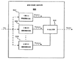
次に図5を参照して、本発明の教示内容に従った例示的なコントローラ500が示される。より具体的には、コントローラ500はパワーコンバータに組込まれて、本発明の教示内容に係る電力スイッチの電流制限を調節することによってバイアス巻線電圧を調節し得る。動作時、コントローラ500は、パワーコンバータの電力スイッチを通るピーク電流を制御する。コントローラ500内で電流制限を調節することによって、電力スイッチを通るピーク電流を制御することができるため、バイアス巻線電圧を調節することができる。一例では、電力スイッチ内のスイッチ電流が電流制限に達したことを電流検知信号USENSEが検出すると、スイッチング信号USWがドライバ回路506から出力されて、電力スイッチをディスエーブルにする。パワーコンバータ500の図示される例は、コントローラ電源502、保護回路504、ドライバ回路506、発振器508、フィードバック回路510、および電流制限調節回路512を含む。示されるように、コントローラ500は電力信号UPOWER、フィードバック信号UFB、および電流検知信号USENSEを受信し、スイッチング信号USWを出力して電力スイッチを切換える。一例では、コントローラ電源502、保護回路504、ドライバ回路506、発振器508、フィードバック回路510、電力信号UPOWER、フィードバック信号UFB、およびスイッチング信号USWは、それぞれ図4のコントローラ電源402、保護回路404、ドライバ回路406、発振器408、フィードバック回路410、電力信号UPOWER、フィードバック信号UFB、およびスイッチング信号USWの可能性のある実現例を表わし得る。
Turning now to FIG. 5, an
示されるように、ドライバ回路506は検知信号USENSEを受信する。一例では、検知信号USENSEは、パワーコンバータの電力スイッチを導通するスイッチ電流を表わす。動作時、ドライバ回路506は電力スイッチを通る電流を制御して、パワーコンバータのバイアス巻線の両端の電圧を調節する。一例では、ドライバ回路506は、パワーコンバータの出力に結合された負荷に供給される出力電流に応じて、電力スイッチの電流制限を調節する。示されるように、電流制限調節回路512はドライバ回路506に結合される。動作時、電流制限調節回路512は、ドライバ回路506内の電流制限を調節する調節済み電流制限信号UADJLIMITを出力する。電流制限調節回路512はドライバ回路506からスイッチング信号USWを受信して、パワーコンバータの出力における負荷を判断する。一例では、電流制限調節回路512は、パワーコンバータの出力に結合された負荷によって取出される出力電流に応じて、ドライバ回路506内の電流制限をどの程度調節すべきかを判断する。動作時、電流制限調節回路512は、スイッチング信号USWに基づいて、負荷によって取出される出力電流を判断し得る。一例では、電流制限調節回路は、スイッチング信号USWから電力スイッチの有効スイッチング周波数を判断し得る。一例では、電流制限調節回路512は、パワーコンバータの出力に結合された負荷の負荷条件に応じて、ドライバ回路506の電流制限を非線形に調節する。
As shown,
次に図6を参照して、本発明の教示内容に従った例示的な調節可能基準電圧回路600が示される。調節可能基準電圧回路600の図示される例は、第1の閾値調節回路602、第2の閾値調節回路604、N番目の閾値調節回路608、および平均化回路606を含む。示されるように、調節可能電圧基準回路600は、電力スイッチのスイッチングを表わすスイッチング信号USWを受信するように結合され、調節可能電圧基準信号UADJREFを出力するように結合される。一例では、調節可能電圧基準回路600は、図4の調節可
能電圧基準回路の可能性のある実現例であり得る。別の例では、調節可能電圧基準信号UADJREFおよびスイッチング信号USWは、それぞれ図1および図4の調節可能電圧基準信号UADJREFおよびスイッチング信号USWの可能性のある実現例を表わし得る。示されるように、第1の閾値調節回路602は平均化回路606に結合され、パワーコンバータの電力スイッチのスイッチングを表わすスイッチング信号を受信するように結合される。動作時、第1の閾値調節回路602は、基準閾値に対する第1の調節を表わす第1の閾値調節信号UTHRESH1を出力する。一例では、第1の閾値調節回路602は第1の負荷条件を判断し、第1の負荷条件よりも低い負荷を表わす第1の閾値調節信号UTHRESH1を平均化回路606に出力する。別の例では、第2の閾値調節回路604は第2の負荷条件を判断し、第2の負荷条件よりも低い負荷を表わす第2の閾値調節信号UTHRESH2を平均化回路606に出力する。第1および第2の調節回路602および604はそれぞれ、有効スイッチング周波数に応じて負荷条件を判断し得る。
With reference now to FIG. 6, an exemplary adjustable
示されるように、平均化回路606は、第1および第2の閾値調節信号UTHRESH1およびUTHRESH2に応じて、調節済み基準信号UADJREFを出力する。一例では、平均化回路606は、実質的に多数のスイッチング期間の閾値調節信号の平均の演算に応じて調節済み基準電圧信号UADJREFを出力する。したがって、調節済み電圧基準信号UADJREFは大きさが徐々に変化し、2、3のスイッチング期間において実質的に一定であると考えることができる。示されるように、調節可能電圧基準UADJREFに寄与するためのN個の閾値調節回路が存在するように、付加的な閾値回路が追加され得る。第2の閾値調節回路を追加することによって、平均化回路606は、スイッチング信号に応じて調節可能電圧基準UADJREFを非線形に調節する。より具体的には、スイッチング信号を用いて、パワーコンバータの出力に結合された負荷条件を判断することができる。
As shown, the averaging
次に図7を参照して、本発明の教示内容に従った、パワーコンバータのための例示的な集積回路700の概略が図示される。示されるように、集積回路700は、ドレイン端子D、ソース端子S、バイパス端子BP、およびフィードバック端子FBを含む。集積回路700はさらに、電力スイッチ701、(VSUPPLYを調整するための)レギュレータ702、保護回路704、調節可能電圧基準回路706、ドライバ回路708、発振器710、信号コンバータ711、およびフィードバック回路712を含む。一例では、保護回路704、ドライバ回路708、調節可能電圧基準回路706、発振器710およびフィードバック回路712は、図4および図5のそれぞれの対応物の可能性のある実現例を表わし得る。保護回路704はさらに、第1の比較器714および第2の比較器716を含む。ドライバ回路708はさらに、電流制限比較器718、リーディングエッジブランキングLEB回路720、第1のANDゲート722、第2のANDゲート724、第3のANDゲート726、ORゲート728、およびRSフリップフロップ730を含む。
Referring now to FIG. 7, a schematic of an exemplary
示されるように、電力スイッチ701はドレイン端子Dとソース端子Sとの間に結合される。動作時、電力スイッチがオン状態で電流を導通することが可能な場合、スイッチ電流が電力スイッチ701を流れる。レギュレータ702はドレイン端子Dに直接結合されて、電力を受けて集積回路700内の回路に供給する。図示されていないが、レギュレータ702は、調整済み供給電圧を与えて集積回路700内の構成部品に動作用電力を供給するように結合される。第1の比較器714はレギュレータ702に結合される。動作時、比較器714は、供給電圧VSUPPLYを不足電圧基準VUNDERと比較する。供給電圧VSUPPLYが不足電圧基準VUNDERを下回る場合、比較器714はANDゲート722にロー信号を出力して、電力スイッチ701のスイッチングを禁止する。示されるように、第2の比較器716はレギュレータ702に結合される。動作時、比較器716は、供給電圧VSUPPLYを過電圧基準VOVERと比較する。供給電圧VSUPPLYが過電圧基準VOVERよりも大きい場合、比較器716はANDゲート726にロー信号を出力して、電力スイッチ701がターンオンすることを禁止する。
As shown,
示されるように、調節可能電圧基準回路706はフィードバック回路712に結合され、信号コンバータ711からイネーブル信号UENABLEを受信するように結合される。一例では、イネーブル信号UENABLEはスイッチング信号USWから判断され、イネーブルスイッチング期間TSを通してハイであり、ディスエーブルスイッチング期間TSを通してローである。別の例では、電圧基準回路706は、スイッチング信号USWを直接受信し得る。動作時、調節可能電圧基準回路706は、パワーコンバータの出力における負荷条件に応じてフィードバック回路712の電圧基準を調節する。より具体的には、調節可能電圧基準回路706は、信号コンバータ711からイネーブル信号UENABLEの受信に応じて負荷条件を判断する。示されるように、フィードバック回路712はフィードバック端子FBおよび調節可能電圧基準回路706に結合される。動作時、フィードバック回路712は、バイアス巻線電圧信号UVBIASが調節可能電圧基準UADJREFよりも大きい場合、ロー信号を出力して電力スイッチ701のスイッチングを禁止する。図示されるように、発振器710はANDゲート726およびRSフリップフロップ730に結合される。動作時、発振器710はクロック信号UCLOCKを出力して、電力スイッチ701のスイッチング周波数を設定する。一例では、UCLOCKは固定信号である。発振器710はさらに、最大デューティサイクル信号DCMAXを出力して、電力スイッチ701が規定時間の間オン状態になることを防止するように結合される。より具体的には、デューティサイクルは、スイッチング期間TSの全時間に対する電力スイッチ701のオン時間の比率である。
As shown, adjustable
示されるように、電流制限比較器718はANDゲート724に結合される。動作時、電流制限比較器718は、スイッチ電流ISWを電流制限ILIMITと比較する。スイッチ電流が電流制限ILIMITに達すると、比較器718はハイ信号を出力して電力スイッチ701をオフ状態にする。このように、電力スイッチ701を通るスイッチ電流が制御される。示されるように、リーディングエッジブランキング(LEB)回路720は、ANDゲート722の出力およびANDゲート724の入力に結合される。動作時、リーディングエッジブランキング回路720は、電力スイッチ701がオンになる際の電流のスパイクによって電流スイッチ701がオフになるのを防ぐ。より具体的には、LEB回路720は、電流のオーバーシュートによって電流制限比較器718が電流スイッチをあまりにも早くオフ状態に切換えないように、各オン時間の開始を遅延させる。
As shown,
示されるように、ORゲート728は、信号を出力して電力スイッチ701をオン状態からオフ状態に切換えるように結合される。ANDゲート726は、信号を出力して電力スイッチ701をオフ状態からオン状態に切換えるように結合される。示されるように、RSフリップフロップ730はANDゲート726およびORゲート728に結合される。動作時、RSフリップフロップ730は、ANDゲート726およびORゲート728からの出力に応じてスイッチング信号USWを出力するように結合される。電流源732は、フィードバック端子FBからの電流を受けるように結合される。
As shown, OR
次に図8を参照して、本発明の教示内容に従った例示的な調節可能電圧基準回路800が示される。示されるように、調節可能電圧基準回路800は、第1の閾値調節回路802、第2の閾値調節回路804、反転器805、および平均化回路806を含む。一例では、閾値調節回路802、閾値調節回路804、および平均化回路806は、それぞれ図6の第1の閾値調節回路602、第2の閾値調節回路604、および平均化回路606の可能性のある実現例であり得る。示されるように、閾値調節回路802は、nチャネルトランジスタ808、pチャネルトランジスタ810、電流源812、キャパシタ814、および反転器816を含む。同様に、閾値調節回路804は、nチャネルトランジスタ818、pチャネルトランジスタ820、電流源822、キャパシタ824、および反転器826を含む。さらに示されるように、平均化回路806は、電流源828、電流源830、電流源832、電流源834、抵抗器836、抵抗器838、キャパシタ840、n
チャネルトランジスタ842、nチャネルトランジスタ844、およびnチャネルトランジスタ846を含む。より具体的には、nチャネルトランジスタおよびpチャネルトランジスタは、nチャネルをオンにする論理信号はpチャネルをオフにするように、反対の機能を実行する。
Referring now to FIG. 8, an exemplary adjustable
示されるように、トランジスタ842は反転イネーブル信号UENを受信するように結合される。1つの実施例によると、イネーブル信号UENABLEはイネーブルまたはディスエーブルスイッチング期間を表わす。より具体的には、イネーブル信号UENABLEは、電力スイッチが導通しているスイッチング期間(イネーブル期間)を通してずっとハイであり、電力スイッチが導通していないスイッチング期間(ディスエーブルスイッチング期間)を通してずっとローである。動作時、反転イネーブル信号UENはディスエーブルスイッチング期間中にハイになり(すなわち、このスイッチング期間中は電力スイッチはターンオンしない)、トランジスタ842がターンオンされて電流を通す。より具体的には、電流源828が、トランジスタ842を導通する電流を与える。このように、抵抗器836を通る電流が電流源828からの電流の量だけ減少するため、抵抗器836の両端の電圧が減少する。例示的な実施例によると、電力スイッチがスイッチング期間中にスイッチングしないたびに、抵抗器836の両端の電圧がある量だけ減少する。動作時、キャパシタ840は、抵抗器836の両端の電圧を平均化する。一例では、ディスエーブルスイッチング期間の後にイネーブル信号UENABLEがイネーブルにされると、トランジスタ842がターンオフし、電流源834の全電流がキャパシタ840を充電して調節可能電圧基準VADJREFを最大値にまで上昇させることができる。x個のスイッチング期間が連続してディスエーブルにされると、トランジスタ844がターンオンし、抵抗器836の両端の電圧がより大量にいずれかのその後の連続ディスエーブルスイッチ期間中に減少するため、電圧VADJREFがより大きな比率で減少する。x個のスイッチング期間が連続してディスエーブルにされると、トランジスタ846がターンオンし、キャパシタ840がより大量にディスエーブルスイッチング期間ごとに放電する。一例では、x個のスイッチング期間はy個のスイッチング期間よりも少ない。たとえば、x個のスイッチング期間は5であり得、y個のスイッチング期間は10であり得る。xおよびyの値は、それぞれキャパシタ814および824のサイズによって決定され得る。より具体的には、キャパシタ814または824のサイズが増加すると、キャパシタ814または824の電圧が十分低くなってトランジスタ844または846のいずれか一方を起動して調節可能基準電圧VADJREFをさらに減少させる前に、さらなるディスエーブルスイッチング期間が経過する必要がある。したがって、パワーコンバータの出力に供給される出力電流が減少するにつれて、このように電圧基準を調節することによってバイアス電圧が非線形に調節され、パワーコンバータの出力における出力電圧が所望の値に保たれる。一例では、調節可能電圧回路800は、フィードバック電圧基準の変化率の分解能を向上させるための付加的な閾値調節回路を含み得る。
As shown,
示されるように、第1の電圧閾値調節回路802は、反転イネーブル信号UENを受信するように結合される。示されるように、電圧源VSUPPLYはトランジスタ810に結合される。動作時、イネーブル信号UENがハイである場合、トランジスタ808はターンオンされトランジスタ810はターンオフされ、キャパシタ814は供給電圧VSUPPLYの当初電圧から放電する。キャパシタ814がx個のスイッチング期間中放電すると、反転器816はハイ信号を出力する。このように、トランジスタ844は起動されてターンオンし、抵抗器836の両端の電圧はその後のディスエーブルスイッチング期間中さらに減少して、フィードバック電圧基準VREFの変化率をさらに高める。同様に、第2の電圧閾値調節回路804は、反転イネーブル信号UENを受信するように結合される。示されるように、電圧源VSUPPLYはトランジスタ820に結合される。動作時、反転イネーブル信号UENがハイである場合、トランジスタ818はターンオンされ、トランジスタ820はターンオフされ、キャパシタ824は供給電圧VSUPPLYから放電する。キャパシタ824がy個の
スイッチング期間中放電すると、反転器826はハイ信号を出力する。このように、トランジスタ846は起動されてターンオンし、キャパシタ840の電圧は減少して、フィードバック電圧基準VREFの変化率をさらに高める。示されるように、キャパシタ840は抵抗器838および抵抗器836を介して放電するように結合される。一例では、キャパシタ840は、電力スイッチのスイッチング期間の時間枠に関して比較的高い時定数を有する。これによって、電圧基準VREFが複数のスイッチング期間にわたって徐々に変化することが可能となる。一例では、抵抗器838の値は14MWであり、キャパシタ840の値は14pFである。
As shown, the first voltage
次に図9を参照して、グラフ900は、負荷条件に応じた図8の電圧基準VREFを示す。示されるように、出力電流IOUTなしの電圧基準波形902の変化は、ゼロにより近い出力電流についてより大きい。すなわち、図示される例では、電圧基準波形902の傾きは、ゼロと第2の閾値との間の出力電流に対して最も大きい。電圧基準波形902はさらに、第2の閾値と第1の閾値との間の出力電流に対しての異なる(たとえばより小さい)傾き、および第1の閾値よりも大きい出力電流に対しての第3の傾き(たとえばさらに小さい)を含む。したがって一例では、基準電圧の非線形の調節は、各々が異なる傾きを有する複数の線形部分を含み得る。このように、調節可能電圧基準は、パワーコンバータの出力における所望の出力電圧をより正確に維持するために区分的に線形に設計される。
Referring now to FIG. 9, a
次に図10を参照して、フローチャートは、一次側フィードバックパワーコンバータの調整を向上させるための方法1000を示す。より具体的には、方法1000は、バイアス電圧が負荷条件に応じて非線形に減少するように、調節可能基準電圧を非線形に減少させる。処理ブロック1010において、コントローラは、調節可能電圧基準に応じてパワーコンバータの出力電圧を調整する。決定ブロック1020において、負荷が第1の負荷条件よりも小さい場合、方法1000は決定ブロック1030に進む。そうでない場合、方法1000は決定ブロック1010に戻る。一例では、第1の負荷条件は、パワーコンバータの電力スイッチのスイッチング周波数に応じて判断され得る。処理ブロック1030において、コントローラは、負荷に応じて第1の比率で調節可能基準電圧の減少を開始する。処理ブロック1040において、負荷が第2の負荷条件よりも小さいか否かが判断される。負荷が第2の負荷条件よりも小さい場合、方法1000はブロック1050に進む。そうでない場合、方法1000は1030に戻る。処理ブロック1050において、調節可能基準電圧の減少率は、負荷に応じてさらに増加する。一例では、第2の比率は第1の比率よりも高い。動作時、負荷条件が無負荷条件(負荷が消費する出力電力がゼロ)に向かうにつれて、調節可能基準電圧は負荷に応じてより速い比率で減少する。一例では、調節可能基準電圧を調節するために2つよりも多い比率が用いられ得る。上述のように、フィードバック電圧基準を調節することによってバイアス巻線電圧が調節される。調節可能基準電圧とバイアス電圧との間に比例関係が存在するため、このようにして、方法1000は負荷条件に応じてバイアス電圧を非線形に調節する。
Referring now to FIG. 10, a flowchart shows a
100 パワーコンバータ、102 集積回路、104 コントローラ、105 入力リターン、106 電力スイッチ、107 出力リターン、108 エネルギ伝達素子、110 フィードバック回路。 100 power converter, 102 integrated circuit, 104 controller, 105 input return, 106 power switch, 107 output return, 108 energy transfer element, 110 feedback circuit.
Claims (29)
スイッチング信号を出力して電力スイッチをオン状態とオフ状態との間で切換えて前記パワーコンバータの出力を調整するように構成されたドライバ回路と、
前記ドライバ回路に結合され、電圧基準と前記パワーコンバータのバイアス巻線電圧との比較に応じてイネーブル信号を出力して前記電力スイッチをオン状態に切換えるように結合されたフィードバック回路と、
前記パワーコンバータの出力における負荷条件に応じて前記バイアス巻線電圧が非線形に調節されるように前記電圧基準を調節するよう構成された調節可能電圧基準回路とを備え、
前記調節可能電圧基準回路は、前記スイッチング信号の有効スイッチング周波数に応答して前記負荷条件を検出するようにさらに構成され、前記スイッチング信号の前記有効スイッチング周波数は、負荷によって取り出される出力電流を示す、コントローラ。 A controller for a primary side control power converter,
A driver circuit configured to adjust the output of the power converter by switching a power switch between an on state and an off state by outputting a switching signal;
A feedback circuit coupled to the driver circuit and coupled to output an enable signal in response to a comparison between a voltage reference and a bias winding voltage of the power converter to switch the power switch to an on state;
And a adjustable voltage reference circuit configured to the bias winding voltage adjusts the voltage reference to be adjusted non-linearly depending on the load condition at the output of the power converter,
The adjustable voltage reference circuit is further configured to detect the load condition in response to an effective switching frequency of the switching signal , the effective switching frequency of the switching signal indicating an output current drawn by a load ; controller.
前記ドライバ回路は、前記負荷条件に応じて前記電力スイッチの電流を制限する、請求項1に記載のコントローラ。 A current sensor outputs a current sense signal representing a switch current through the power switch;
The controller according to claim 1, wherein the driver circuit limits a current of the power switch according to the load condition.
前記発振器はクロック信号を出力して、前記電力スイッチの実質的に一定のスイッチング周期を設定する、請求項1に記載のコントローラ。 Further comprising an oscillator coupled to the driver circuit;
The controller of claim 1, wherein the oscillator outputs a clock signal to set a substantially constant switching period of the power switch.
前記第1の閾値調節回路は、第1の出力電流に関連した第1の負荷条件に応じて第1の量だけ前記電圧基準を調節する、請求項3に記載のコントローラ。 The adjustable voltage reference circuit further includes a first threshold adjustment circuit;
4. The controller of claim 3, wherein the first threshold adjustment circuit adjusts the voltage reference by a first amount in response to a first load condition associated with a first output current .
前記第2の閾値調節回路は、第2の出力電流に関連した第2の負荷条件に応じて第2の量だけ前記電圧基準を調節し、
前記第1の量から前記第2の量への相対的変化は、前記第1の出力電流から前記第2の出力電流への相対的変化よりも大きい相対的変化である、請求項5に記載のコントローラ。 The adjustable voltage reference circuit further includes a second threshold adjustment circuit;
The second threshold adjustment circuit adjusts the voltage reference by a second amount in response to a second load condition associated with a second output current ;
It said first relative changes from quantity to the second quantity is the relative change is greater than the relative change from the first output current to said second output current, according to claim 5 Controller.
オン状態とオフ状態との間で切換わるように構成された電力スイッチと、
スイッチング信号を用いて前記電力スイッチをオン状態とオフ状態との間で切換えて前記パワーコンバータの出力を調整するように構成され、前記電力スイッチを流れるスイッチ電流がスイッチ電流閾値に達したことおよび前記パワーコンバータの出力電圧を表わすバイアス巻線電圧に応じて前記電力スイッチをディスエーブルにするように適合されたコントローラと、
前記コントローラに結合され、前記バイアス巻線電圧を受けるフィードバック端子とを備え、
前記コントローラは、前記パワーコンバータの出力における負荷条件に応じて前記バイアス巻線電圧を非線形に調節するように結合され、
前記コントローラは、前記スイッチング信号の有効スイッチング周波数に応答して前記負荷条件を検出し、前記スイッチング信号の前記有効スイッチング周波数は、負荷によって取り出される出力電流を示す、集積回路。 An integrated circuit for a power converter,
A power switch configured to switch between an on state and an off state;
It said power switch with a switching signal is switched between an on state and an off state is configured to adjust the output of the power converter, the possible and the switch current reaches the switch current threshold through the power switch A controller adapted to disable the power switch in response to a bias winding voltage representative of the output voltage of the power converter ;
Coupled to the controller, and a feedback terminal for receiving the bias winding voltage,
The controller is coupled to nonlinearly adjust the bias winding voltage in response to a load condition at the output of the power converter;
The integrated circuit, wherein the controller detects the load condition in response to an effective switching frequency of the switching signal, and the effective switching frequency of the switching signal indicates an output current drawn by a load .
電力スイッチと、
前記電力スイッチに結合され、スイッチング信号を用いて前記電力スイッチをオン状態とオフ状態との間で切換えてバイアス巻線電圧に応じて前記パワーコンバータの出力を調整するコントローラと、
前記電力スイッチに結合され、前記パワーコンバータの入力を出力からガルバニック絶縁し、かつ前記パワーコンバータの入力と出力との間でエネルギを伝達するエネルギ伝達素子と、
前記エネルギ伝達素子に結合されたバイアス巻線とを備え、
前記バイアス巻線の両端の前記バイアス巻線電圧は、前記パワーコンバータの出力における出力電圧を表わし、
前記コントローラは、前記パワーコンバータの出力における負荷条件に応じて前記バイアス巻線電圧を非線形に調節し、
前記コントローラは、前記スイッチング信号の有効スイッチング周波数に応答して前記負荷条件を検出し、前記スイッチング信号の前記有効スイッチング周波数は、負荷によって取り出される出力電流を示す、パワーコンバータ。 A power converter,
A power switch;
A controller coupled to the power switch and switching the power switch between an on state and an off state using a switching signal to adjust the output of the power converter in response to a bias winding voltage ;
An energy transfer element coupled to the power switch to galvanically isolate the input of the power converter from the output and to transfer energy between the input and output of the power converter;
A bias winding coupled to the energy transfer element;
The bias winding voltage across the bias winding, represents the output voltage at the output of the power converter,
The controller adjusts the bias winding voltage nonlinearly according to a load condition at the output of the power converter,
The controller detects the load condition in response to an effective switching frequency of the switching signal, and the effective switching frequency of the switching signal indicates an output current drawn by a load .
スイッチング信号を用いてバイアス巻線電圧に応じて電力スイッチをオン状態とオフ状態との間で切換えることによってパワーコンバータの出力電圧を調整するステップを備え、前記電力スイッチは、前記電力スイッチを通るスイッチ電流がスイッチ電流がスイッチ電流閾値を超えるとオフ状態に戻るように適合され、前記方法はさらに、
前記スイッチング信号の有効スイッチング周波数に応答して前記パワーコンバータの出力に結合された負荷の負荷条件を判断するステップとを備え、前記スイッチング信号の前記有効スイッチング周波数は、負荷によって取り出される出力電流を示し、前記方法は、
前記負荷条件に応じて前記バイアス巻線電圧を非線形に調節するステップをさらに備える、方法。 A method for adjusting a bias winding voltage of a power supply, comprising:
Adjusting the output voltage of the power converter by switching the power switch between an on state and an off state in response to a bias winding voltage using a switching signal, the power switch passing through the power switch The current is adapted to return to an off state when the switch current exceeds a switch current threshold, the method further comprising:
And a step of determining the load condition of the coupled to an output of the power converter in response to the effective switching frequency of the switching signal load, the effective switching frequency of the switching signal indicates the output current drawn by the load The method
Further comprising, methods steps for adjusting the bias winding voltage nonlinearly in response to the load condition.
前記バイアス巻線電圧が前記調節可能基準電圧よりも大きい場合、前記電力スイッチのスイッチングを禁止するステップを備える、請求項19に記載のバイアス巻線電圧を調節するための方法。 Adjusting the bias winding voltage nonlinearly in response to the load condition comprises adjusting the adjustable reference voltage nonlinearly, the method further comprising:
The method for adjusting a bias winding voltage according to claim 19 , comprising inhibiting switching of the power switch if the bias winding voltage is greater than the adjustable reference voltage.
スイッチング信号を出力して電力スイッチをオン状態とオフ状態との間で切換えて前記パワーコンバータの出力を調整するように構成されたドライバ回路と、
前記ドライバ回路に結合され、出力電圧信号に応じてイネーブル信号を出力して前記電力スイッチをオン状態に切換えるように結合されたフィードバック回路と、
電流検知信号を受信し、かつスイッチ電流がスイッチ電流閾値に達すると前記電力スイッチをオフ状態に切換えるように構成された電流制限回路と、
前記パワーコンバータの出力における負荷条件に応じて前記パワーコンバータのバイアス巻線電圧が非線形に調節されるように電流制限を調節するよう構成された調節可能電圧基準回路とを備え、
前記調節可能電圧基準回路は、前記スイッチング信号の有効スイッチング周波数に応答して前記負荷条件を検出するようにさらに結合され、前記スイッチング信号の前記有効スイッチング周波数は、負荷によって取り出される出力電流を示す、コントローラ。 A controller for a primary side control power converter,
A driver circuit configured to adjust the output of the power converter by switching a power switch between an on state and an off state by outputting a switching signal;
A feedback circuit coupled to the driver circuit and coupled to output an enable signal in response to an output voltage signal to switch the power switch to an on state;
A current limiting circuit configured to receive a current sense signal and to switch the power switch to an off state when the switch current reaches a switch current threshold;
An adjustable voltage reference circuit configured to adjust a current limit such that a bias winding voltage of the power converter is adjusted nonlinearly in response to a load condition at the output of the power converter;
The adjustable voltage reference circuit is further coupled to detect the load condition in response to an effective switching frequency of the switching signal , the effective switching frequency of the switching signal indicating an output current drawn by a load. ,controller.
スイッチング信号を出力して電力スイッチの切換を制御して前記パワーコンバータの出力を調整するように構成されたドライバ回路と、
前記ドライバ回路に結合され、バイアス巻線電圧が調節可能基準電圧よりも大きい場合、前記電力スイッチのスイッチングを禁止するフィードバック回路と、
前記パワーコンバータの出力における負荷条件に応じて前記調節可能基準電圧を非線形に調節するように構成された調節可能電圧基準回路とを備え、
前記調節可能電圧基準回路は、前記スイッチング信号の有効スイッチング周波数に応答して前記負荷条件を検出するようにさらに結合され、前記スイッチング信号の前記有効スイッチング周波数は、負荷によって取り出される出力電流を示す、コントローラ。 An integrated circuit controller for a power converter,
A driver circuit configured to output a switching signal to control switching of the power switch to adjust the output of the power converter;
A feedback circuit coupled to the driver circuit and prohibiting switching of the power switch if the bias winding voltage is greater than an adjustable reference voltage;
An adjustable voltage reference circuit configured to nonlinearly adjust the adjustable reference voltage in response to a load condition at the output of the power converter;
The adjustable voltage reference circuit is further coupled to detect the load condition in response to an effective switching frequency of the switching signal , the effective switching frequency of the switching signal indicating an output current drawn by a load. ,controller.
前記パワーコンバータの出力における第1の負荷条件に応じて第1の閾値調節信号を出力するように構成された第1の閾値調節回路と、
前記パワーコンバータの出力における第2の負荷条件に応じて第2の閾値調節信号を出力するように構成された第2の閾値調節回路と、
調節可能電圧基準を生成し、かつ前記第1および第2の閾値調節信号に応じて前記調節可能電圧基準を調節するように構成された平均化回路とを備える、請求項24に記載のコントローラ。 The adjustable voltage reference circuit comprises:
A first threshold adjustment circuit configured to output a first threshold adjustment signal in response to a first load condition at the output of the power converter;
A second threshold adjustment circuit configured to output a second threshold adjustment signal in response to a second load condition at the output of the power converter;
25. The controller of claim 24 , comprising: an adjustable voltage reference configured to generate an adjustable voltage reference and to adjust the adjustable voltage reference in response to the first and second threshold adjustment signals.
前記キャパシタはさらに、前記第1および第2の閾値調節信号に応じて選択的に放電するように結合される、請求項25に記載のコントローラ。 The averaging circuit comprises a capacitor coupled to store the adjustable voltage reference;
26. The controller of claim 25 , wherein the capacitor is further coupled to selectively discharge in response to the first and second threshold adjustment signals.
前記第1の電流源は、前記第1の閾値調節信号に応じて第1の比率で前記キャパシタの両端の平均電圧を減少させるように結合され、
前記第2の電流源は、前記第2の閾値調節信号に応じて第2の比率で前記キャパシタの両端の平均電圧を減少させるように結合される、請求項26に記載のコントローラ。 The averaging circuit further comprises first and second current sources,
The first current source is coupled to decrease to less of the average voltage across the capacitor at a first ratio in response to said first threshold adjustment signal,
27. The controller of claim 26 , wherein the second current source is coupled to reduce an average voltage across the capacitor by a second ratio in response to the second threshold adjustment signal.
前記第2の閾値調節回路は、前記スイッチング信号の第2の数の連続ディスエーブルスイッチング周期に応じて前記第2の閾値調節信号を出力するように結合される、請求項25に記載のコントローラ。 The first threshold adjustment circuit is coupled to output the first threshold adjustment signal in response to a first number of consecutive disable switching periods of the switching signal;
26. The controller of claim 25 , wherein the second threshold adjustment circuit is coupled to output the second threshold adjustment signal in response to a second number of consecutive disable switching periods of the switching signal.
Applications Claiming Priority (2)
| Application Number | Priority Date | Filing Date | Title |
|---|---|---|---|
| US12/363,657 | 2009-01-30 | ||
| US12/363,657 US8159843B2 (en) | 2009-01-30 | 2009-01-30 | Method and apparatus to regulate an output voltage of a power converter at light/no load conditions |
Publications (3)
| Publication Number | Publication Date |
|---|---|
| JP2010178618A JP2010178618A (en) | 2010-08-12 |
| JP2010178618A5 JP2010178618A5 (en) | 2013-03-07 |
| JP5652731B2 true JP5652731B2 (en) | 2015-01-14 |
Family
ID=42125950
Family Applications (1)
| Application Number | Title | Priority Date | Filing Date |
|---|---|---|---|
| JP2010013764A Expired - Fee Related JP5652731B2 (en) | 2009-01-30 | 2010-01-26 | Controller for primary side controlled power converter, integrated circuit for power converter, power converter, method for adjusting bias winding voltage of power supply, and integrated circuit controller for power converter |
Country Status (4)
| Country | Link |
|---|---|
| US (3) | US8159843B2 (en) |
| EP (2) | EP2224583A1 (en) |
| JP (1) | JP5652731B2 (en) |
| CN (2) | CN103997227A (en) |
Families Citing this family (33)
| Publication number | Priority date | Publication date | Assignee | Title |
|---|---|---|---|---|
| US8604763B2 (en) * | 2009-08-31 | 2013-12-10 | Decicon, Inc. | Power delivery system with surge handling capability |
| KR20160121591A (en) * | 2010-08-18 | 2016-10-19 | 핀식스 코포레이션 | Very high frequency switching cell-based power converter |
| US8922185B2 (en) * | 2011-07-11 | 2014-12-30 | Solarbridge Technologies, Inc. | Device and method for global maximum power point tracking |
| US8693217B2 (en) * | 2011-09-23 | 2014-04-08 | Power Integrations, Inc. | Power supply controller with minimum-sum multi-cycle modulation |
| US9071152B2 (en) | 2012-07-03 | 2015-06-30 | Cognipower, Llc | Power converter with demand pulse isolation |
| DK177701B1 (en) * | 2012-07-10 | 2014-03-24 | Pr Electronics As | Magnetic balanced converter with isolation barrier |
| WO2014066266A1 (en) * | 2012-10-24 | 2014-05-01 | Marvell World Trade Ltd. | Method and apparatus to reduce overcurrent during the startup of a switching regulator |
| US9164133B2 (en) * | 2012-11-02 | 2015-10-20 | Power Integrations, Inc. | Switched averaging error amplifier |
| CN103052247B (en) * | 2012-11-23 | 2016-04-27 | 中国电子科技集团公司第四十五研究所 | The starting current limiting circuit of ultrahigh pressure mercury lamp in a kind of lithographic equipment |
| CN102946204B (en) * | 2012-11-30 | 2015-01-07 | 无锡中星微电子有限公司 | AC-DC (Alternating Current-Direct Current) regulator and regulating method |
| US9280164B2 (en) * | 2013-01-18 | 2016-03-08 | Sanken Electric Co., Ltd. | Switching power-supply device and method for manufacturing switching power-supply device |
| CN103078500B (en) * | 2013-02-08 | 2015-08-26 | 广州视源电子科技股份有限公司 | Adjustable switch power supply |
| US9246392B2 (en) | 2013-03-13 | 2016-01-26 | Power Integrations, Inc. | Switched mode power converter controller with ramp time modulation |
| US9627915B2 (en) * | 2013-03-15 | 2017-04-18 | Flextronics Ap, Llc | Sweep frequency mode for multiple magnetic resonant power transmission |
| US11083067B2 (en) * | 2013-03-15 | 2021-08-03 | Hatch Transformers, Inc. | Electrical power supply with removable plug-in cartridge |
| US9601982B1 (en) | 2013-08-27 | 2017-03-21 | Flextronics Ap, Llc | Switchable auxiliary supply circuit |
| JP6213087B2 (en) * | 2013-09-18 | 2017-10-18 | 富士電機株式会社 | Isolated switching power supply |
| WO2015157395A2 (en) * | 2014-04-08 | 2015-10-15 | Rompower Energy Systems Inc. | Optimum offline converter control using intelligent power processing |
| US9520769B2 (en) | 2014-04-30 | 2016-12-13 | Stmicroelectronics S.R.L. | Wake up management circuit for a switching converter and related wake up method |
| US10056829B2 (en) * | 2014-08-07 | 2018-08-21 | Panasonic Intellectual Property Management Co., Ltd. | In-vehicle power supply device and vehicle mounted with same |
| US9774248B2 (en) | 2014-11-10 | 2017-09-26 | Power Integrations, Inc. | Introducing jitter to a switching frequency by way of modulating current limit |
| CN104483580B (en) * | 2014-12-25 | 2017-03-29 | 珠海全志科技股份有限公司 | A kind of DC DC transducers zero load detection means based on PFM step-by-step countings |
| US9450478B1 (en) * | 2015-04-10 | 2016-09-20 | Power Integrations, Inc. | Load responsive jitter |
| US10418906B2 (en) * | 2015-09-30 | 2019-09-17 | Apple Inc. | High efficiency primary and secondary bias flyback converter with dual outputs |
| WO2018033771A1 (en) * | 2016-08-16 | 2018-02-22 | Telefonaktiebolaget Lm Ericsson (Publ) | Power converter to produce a reference voltage and method of operating the same |
| CN107508468B (en) * | 2016-08-29 | 2023-05-16 | 杰华特微电子股份有限公司 | Control circuit and method of isolated switching power supply and isolated switching power supply |
| CN109075714B (en) * | 2017-03-31 | 2023-04-14 | 雅达电子国际有限公司 | Switched mode power supply with burst mode operation for reduced power consumption |
| CN107947586A (en) * | 2017-11-07 | 2018-04-20 | 陕西亚成微电子股份有限公司 | A kind of Switching Power Supply fast-response control circuit and control method |
| US10243442B1 (en) | 2017-11-22 | 2019-03-26 | Power Integrations, Inc. | Controller with frequency to on-time converter |
| US10505458B1 (en) * | 2018-10-22 | 2019-12-10 | Power Integrations, Inc. | Apparatus and methods for controlling a switch mode power converter using a duty cycle state machine |
| US11476768B2 (en) * | 2020-02-19 | 2022-10-18 | Alpha And Omega Semiconductor International Lp | Flyback converter for controlling on time variation |
| CN114944763B (en) * | 2022-07-25 | 2022-10-28 | 陕西中科天地航空模块有限公司 | Switching power supply frequency regulating circuit |
| CN116780478A (en) * | 2023-07-25 | 2023-09-19 | 深圳市正浩创新科技股份有限公司 | Overload protection method of inverter circuit and electronic equipment |
Family Cites Families (24)
| Publication number | Priority date | Publication date | Assignee | Title |
|---|---|---|---|---|
| US3541420A (en) * | 1968-03-27 | 1970-11-17 | Motorola Inc | Voltage converter and regulator |
| JPH0626469B2 (en) * | 1988-04-28 | 1994-04-06 | 株式会社日立製作所 | Magnetron drive |
| US5101335A (en) | 1990-12-26 | 1992-03-31 | Eastman Kodak Company | DC-to-DC converter using coupled inductor current sensing and predetermined on time |
| US5313381A (en) * | 1992-09-01 | 1994-05-17 | Power Integrations, Inc. | Three-terminal switched mode power supply integrated circuit |
| US5335162A (en) * | 1993-01-15 | 1994-08-02 | Toko America, Inc. | Primary side controller for regulated power converters |
| US5710697A (en) * | 1996-03-26 | 1998-01-20 | Unitrode Corporation | Power supply controller having frequency foldback and volt-second duty cycle clamp features |
| US5734564A (en) * | 1996-07-26 | 1998-03-31 | Lucent Technologies Inc. | High-efficiency switching power converter |
| JP3175663B2 (en) * | 1997-10-17 | 2001-06-11 | 株式会社村田製作所 | Self-oscillation type switching power supply |
| JPH11235028A (en) * | 1998-02-13 | 1999-08-27 | Murata Mfg Co Ltd | Switching power supply |
| AT408294B (en) | 1998-09-30 | 2001-10-25 | Siemens Ag Oesterreich | LOCK CONVERTER |
| US6249876B1 (en) * | 1998-11-16 | 2001-06-19 | Power Integrations, Inc. | Frequency jittering control for varying the switching frequency of a power supply |
| AU5299600A (en) * | 1999-05-26 | 2000-12-12 | Broadcom Corporation | Integrated vco |
| TW459438B (en) * | 1999-09-17 | 2001-10-11 | Koninkl Philips Electronics Nv | Multimode switched-mode power supply |
| US6525514B1 (en) * | 2000-08-08 | 2003-02-25 | Power Integrations, Inc. | Method and apparatus for reducing audio noise in a switching regulator |
| JP3371962B2 (en) * | 2000-12-04 | 2003-01-27 | サンケン電気株式会社 | DC-DC converter |
| JP3391384B2 (en) * | 2000-12-04 | 2003-03-31 | サンケン電気株式会社 | DC-DC converter |
| US7262628B2 (en) * | 2004-07-02 | 2007-08-28 | Primarion, Inc. | Digital calibration with lossless current sensing in a multiphase switched power converter |
| US6912136B2 (en) * | 2003-04-01 | 2005-06-28 | Maxwell Technologies, Inc. | Switching power supply |
| US7388764B2 (en) * | 2005-06-16 | 2008-06-17 | Active-Semi International, Inc. | Primary side constant output current controller |
| US7233504B2 (en) * | 2005-08-26 | 2007-06-19 | Power Integration, Inc. | Method and apparatus for digital control of a switching regulator |
| US7936159B2 (en) * | 2007-03-23 | 2011-05-03 | Power Integrations, Inc. | Method and apparatus for a high voltage power supply circuit |
| TW200847602A (en) * | 2007-05-29 | 2008-12-01 | Richtek Techohnology Corp | Apparatus and method of improving flyback transformer light-loading efficacy |
| JP2010022121A (en) * | 2008-07-10 | 2010-01-28 | Panasonic Corp | Switching power supply device and semiconductor device for switching power supply |
| US7876583B2 (en) * | 2008-12-22 | 2011-01-25 | Power Integrations, Inc. | Flyback power supply with forced primary regulation |
-
2009
- 2009-01-30 US US12/363,657 patent/US8159843B2/en not_active Expired - Fee Related
-
2010
- 2010-01-25 EP EP10151572A patent/EP2224583A1/en not_active Withdrawn
- 2010-01-25 EP EP12168097A patent/EP2490327A1/en not_active Withdrawn
- 2010-01-26 JP JP2010013764A patent/JP5652731B2/en not_active Expired - Fee Related
- 2010-01-29 CN CN201410255704.3A patent/CN103997227A/en active Pending
- 2010-01-29 CN CN201010107598.6A patent/CN101795075B/en not_active Expired - Fee Related
-
2012
- 2012-03-02 US US13/411,297 patent/US8374006B2/en not_active Expired - Fee Related
-
2013
- 2013-01-09 US US13/737,791 patent/US8913407B2/en not_active Expired - Fee Related
Also Published As
| Publication number | Publication date |
|---|---|
| US8913407B2 (en) | 2014-12-16 |
| CN101795075A (en) | 2010-08-04 |
| US8159843B2 (en) | 2012-04-17 |
| CN103997227A (en) | 2014-08-20 |
| US20100194367A1 (en) | 2010-08-05 |
| CN101795075B (en) | 2014-07-16 |
| JP2010178618A (en) | 2010-08-12 |
| US20120163043A1 (en) | 2012-06-28 |
| EP2224583A1 (en) | 2010-09-01 |
| US8374006B2 (en) | 2013-02-12 |
| US20130121040A1 (en) | 2013-05-16 |
| EP2490327A1 (en) | 2012-08-22 |
Similar Documents
| Publication | Publication Date | Title |
|---|---|---|
| JP5652731B2 (en) | Controller for primary side controlled power converter, integrated circuit for power converter, power converter, method for adjusting bias winding voltage of power supply, and integrated circuit controller for power converter | |
| US8243478B2 (en) | Method and apparatus for limiting maximum output power of a power converter | |
| US9293996B2 (en) | Method and apparatus for integrated cable drop compensation of a power converter | |
| US8614872B2 (en) | Switching power source apparatus | |
| EP1744441B1 (en) | Method and apparatus to limit output power in a switching power supply | |
| US8519691B2 (en) | Current limiting for DC-DC converters | |
| JP5016268B2 (en) | Method and apparatus for limiting the maximum switch current in a switching power supply | |
| JP5334438B2 (en) | Method and apparatus for high voltage power supply circuit | |
| JP5424442B2 (en) | Device for adjusting diode conduction duty cycle | |
| US10069403B1 (en) | Power supply with low power standby mode having fixed burst-on time and adaptive LLC burst frequency adjustment | |
| WO2006095328A2 (en) | Switched mode power converter and method of operation thereof | |
| WO2008071094A1 (en) | Method and circuit for providing compensations of current mode power converters | |
| US9054591B2 (en) | Switching power supply apparatus and method of controlling switching power supply apparatus |
Legal Events
| Date | Code | Title | Description |
|---|---|---|---|
| A521 | Request for written amendment filed |
Free format text: JAPANESE INTERMEDIATE CODE: A523 Effective date: 20130111 |
|
| A621 | Written request for application examination |
Free format text: JAPANESE INTERMEDIATE CODE: A621 Effective date: 20130111 |
|
| A131 | Notification of reasons for refusal |
Free format text: JAPANESE INTERMEDIATE CODE: A131 Effective date: 20140225 |
|
| A521 | Request for written amendment filed |
Free format text: JAPANESE INTERMEDIATE CODE: A523 Effective date: 20140526 |
|
| TRDD | Decision of grant or rejection written | ||
| A01 | Written decision to grant a patent or to grant a registration (utility model) |
Free format text: JAPANESE INTERMEDIATE CODE: A01 Effective date: 20141021 |
|
| A61 | First payment of annual fees (during grant procedure) |
Free format text: JAPANESE INTERMEDIATE CODE: A61 Effective date: 20141107 |
|
| R150 | Certificate of patent or registration of utility model |
Ref document number: 5652731 Country of ref document: JP Free format text: JAPANESE INTERMEDIATE CODE: R150 |
|
| R250 | Receipt of annual fees |
Free format text: JAPANESE INTERMEDIATE CODE: R250 |
|
| LAPS | Cancellation because of no payment of annual fees |