JP5649810B2 - Capacitive sensor - Google Patents
Capacitive sensor Download PDFInfo
- Publication number
- JP5649810B2 JP5649810B2 JP2009249424A JP2009249424A JP5649810B2 JP 5649810 B2 JP5649810 B2 JP 5649810B2 JP 2009249424 A JP2009249424 A JP 2009249424A JP 2009249424 A JP2009249424 A JP 2009249424A JP 5649810 B2 JP5649810 B2 JP 5649810B2
- Authority
- JP
- Japan
- Prior art keywords
- signal
- unit
- capacitance
- frequency
- movable
- Prior art date
- Legal status (The legal status is an assumption and is not a legal conclusion. Google has not performed a legal analysis and makes no representation as to the accuracy of the status listed.)
- Expired - Fee Related
Links
Images


Classifications
-
- G—PHYSICS
- G01—MEASURING; TESTING
- G01P—MEASURING LINEAR OR ANGULAR SPEED, ACCELERATION, DECELERATION, OR SHOCK; INDICATING PRESENCE, ABSENCE, OR DIRECTION, OF MOVEMENT
- G01P21/00—Testing or calibrating of apparatus or devices covered by the preceding groups
-
- G—PHYSICS
- G01—MEASURING; TESTING
- G01C—MEASURING DISTANCES, LEVELS OR BEARINGS; SURVEYING; NAVIGATION; GYROSCOPIC INSTRUMENTS; PHOTOGRAMMETRY OR VIDEOGRAMMETRY
- G01C19/00—Gyroscopes; Turn-sensitive devices using vibrating masses; Turn-sensitive devices without moving masses; Measuring angular rate using gyroscopic effects
- G01C19/56—Turn-sensitive devices using vibrating masses, e.g. vibratory angular rate sensors based on Coriolis forces
- G01C19/5719—Turn-sensitive devices using vibrating masses, e.g. vibratory angular rate sensors based on Coriolis forces using planar vibrating masses driven in a translation vibration along an axis
-
- G—PHYSICS
- G01—MEASURING; TESTING
- G01P—MEASURING LINEAR OR ANGULAR SPEED, ACCELERATION, DECELERATION, OR SHOCK; INDICATING PRESENCE, ABSENCE, OR DIRECTION, OF MOVEMENT
- G01P15/00—Measuring acceleration; Measuring deceleration; Measuring shock, i.e. sudden change of acceleration
- G01P15/02—Measuring acceleration; Measuring deceleration; Measuring shock, i.e. sudden change of acceleration by making use of inertia forces using solid seismic masses
- G01P15/08—Measuring acceleration; Measuring deceleration; Measuring shock, i.e. sudden change of acceleration by making use of inertia forces using solid seismic masses with conversion into electric or magnetic values
- G01P15/125—Measuring acceleration; Measuring deceleration; Measuring shock, i.e. sudden change of acceleration by making use of inertia forces using solid seismic masses with conversion into electric or magnetic values by capacitive pick-up
-
- G—PHYSICS
- G01—MEASURING; TESTING
- G01P—MEASURING LINEAR OR ANGULAR SPEED, ACCELERATION, DECELERATION, OR SHOCK; INDICATING PRESENCE, ABSENCE, OR DIRECTION, OF MOVEMENT
- G01P15/00—Measuring acceleration; Measuring deceleration; Measuring shock, i.e. sudden change of acceleration
- G01P15/02—Measuring acceleration; Measuring deceleration; Measuring shock, i.e. sudden change of acceleration by making use of inertia forces using solid seismic masses
- G01P15/08—Measuring acceleration; Measuring deceleration; Measuring shock, i.e. sudden change of acceleration by making use of inertia forces using solid seismic masses with conversion into electric or magnetic values
- G01P2015/0805—Measuring acceleration; Measuring deceleration; Measuring shock, i.e. sudden change of acceleration by making use of inertia forces using solid seismic masses with conversion into electric or magnetic values being provided with a particular type of spring-mass-system for defining the displacement of a seismic mass due to an external acceleration
- G01P2015/0808—Measuring acceleration; Measuring deceleration; Measuring shock, i.e. sudden change of acceleration by making use of inertia forces using solid seismic masses with conversion into electric or magnetic values being provided with a particular type of spring-mass-system for defining the displacement of a seismic mass due to an external acceleration for defining in-plane movement of the mass, i.e. movement of the mass in the plane of the substrate
- G01P2015/0811—Measuring acceleration; Measuring deceleration; Measuring shock, i.e. sudden change of acceleration by making use of inertia forces using solid seismic masses with conversion into electric or magnetic values being provided with a particular type of spring-mass-system for defining the displacement of a seismic mass due to an external acceleration for defining in-plane movement of the mass, i.e. movement of the mass in the plane of the substrate for one single degree of freedom of movement of the mass
- G01P2015/0814—Measuring acceleration; Measuring deceleration; Measuring shock, i.e. sudden change of acceleration by making use of inertia forces using solid seismic masses with conversion into electric or magnetic values being provided with a particular type of spring-mass-system for defining the displacement of a seismic mass due to an external acceleration for defining in-plane movement of the mass, i.e. movement of the mass in the plane of the substrate for one single degree of freedom of movement of the mass for translational movement of the mass, e.g. shuttle type
Description
本発明は、静電容量式センサに関し、特に、故障(異常)の有無を判断する診断機能を備える静電容量式センサに適用して有効な技術に関する。 The present invention relates to a capacitance type sensor, and more particularly to a technique that is effective when applied to a capacitance type sensor having a diagnostic function for determining the presence or absence of a failure (abnormality).
MEMS(Micro Electro Mechanical Systems)センサの1つである加速度センサは、錘(可動部)と支持梁(弾性変形部)とで構成されており、錘に働く加速度を電気信号に変換するものである。このようなMEMSセンサとしては、コンデンサを構成する電極間の容量変化として加速度を検出する静電容量式センサがあり、この静電容量式センサは、錘に働く加速度を容量などの変化として捉え、それをLSI回路で電気信号に変換してMEMSセンサの出力としている。 An acceleration sensor, which is one of MEMS (Micro Electro Mechanical Systems) sensors, includes a weight (movable part) and a support beam (elastic deformation part), and converts acceleration acting on the weight into an electrical signal. . As such a MEMS sensor, there is a capacitance type sensor that detects acceleration as a change in capacitance between electrodes constituting a capacitor. This capacitance type sensor detects acceleration acting on a weight as a change in capacitance, etc. It is converted into an electrical signal by an LSI circuit and used as the output of the MEMS sensor.
例えば、車の横滑りやスピンを抑制して安全な走行を支援する姿勢制御システムには、角速度を検出する角速度センサや、前後方向および横方向の加速度を検出する加速度センサなどのMEMSセンサがキーデバイスとして用いられる。この姿勢制御システムでは、角速度センサや加速度センサからの出力を元にエンジンの出力やブレーキの制動力を制御することで車の横滑りやスピンを抑制している。このことから、角速度センサや加速度センサの故障は事故に繋がる可能性が高く、角速度センサや加速度センサの故障時にはすぐに知らせる必要がある。 For example, in an attitude control system that supports safe driving by suppressing side slip and spin of a car, an MEMS sensor such as an angular velocity sensor that detects angular velocity or an acceleration sensor that detects longitudinal and lateral acceleration is a key device. Used as In this attitude control system, side slip and spin of a vehicle are suppressed by controlling engine output and braking force of a brake based on outputs from an angular velocity sensor and an acceleration sensor. For this reason, the failure of the angular velocity sensor or the acceleration sensor is likely to lead to an accident, and it is necessary to notify immediately when the angular velocity sensor or the acceleration sensor fails.
特開2007−248328号公報(特許文献1)には、加速度に起因して可動する2つの可動電極と、これらの可動電極のそれぞれに対向配置させた2つの検出電極とを有する検知素子と、交流バイアス電圧信号を可動電極に入力するドライブ回路と、2つの検出電極から出力された2つの検出信号に基づいて加速度信号を出力する検出回路とを備える加速度センサが記載されている。そして、この加速度センサの検出回路において、2つの増幅器に入力する基準電圧信号とは別に、検知電圧印加部から検知電圧信号を2つの増幅器に入力して差動検出器から出力される検知差動信号に基づいて故障を検知する故障検知手段を設けているとしている。 Japanese Patent Application Laid-Open No. 2007-248328 (Patent Document 1) discloses a sensing element having two movable electrodes that move due to acceleration, and two detection electrodes that are arranged to face each of these movable electrodes, An acceleration sensor is described that includes a drive circuit that inputs an AC bias voltage signal to a movable electrode and a detection circuit that outputs an acceleration signal based on two detection signals output from two detection electrodes. In addition, in the detection circuit of the acceleration sensor, apart from the reference voltage signal input to the two amplifiers, the detection differential signal input from the detection voltage application unit to the two amplifiers and output from the differential detector. It is assumed that failure detection means for detecting a failure based on the signal is provided.
特開平05−281256号公報(特許文献2)には、検出電極の静電容量を検出するために印加する交流信号に低周波数の診断信号を重畳させることで、可動電極と固定電極間の静電容量を変化させることが記載されている。そして、その結果発生する加速度センサの出力が振動しているか否かを観測することで信号である加速度を検出しながらも加速度センサの故障の有無を判断することができると記載されている。 In Japanese Patent Application Laid-Open No. 05-281256 (Patent Document 2), a low-frequency diagnostic signal is superimposed on an AC signal applied to detect the capacitance of a detection electrode, whereby a static signal between the movable electrode and the fixed electrode is superimposed. It describes changing the capacitance. Further, it is described that by observing whether or not the output of the acceleration sensor generated as a result is oscillating, it is possible to determine the presence or absence of a failure of the acceleration sensor while detecting the acceleration as a signal.
このとき、低周波数の診断信号は加速度の測定に支障が出ない程度の振幅で出力を振動させるため、加速度を検出しながら故障の有無を診断する常時診断が可能であると記載されている。また、診断信号(診断種類の切換信号)がローレベルの場合は、可動電極を大きく強制的に振動させる高加速度診断も可能であると記載されている。 At this time, since the output of the low-frequency diagnostic signal vibrates with an amplitude that does not hinder the measurement of acceleration, it is described that it is possible to always diagnose whether there is a failure while detecting the acceleration. Further, it is described that when the diagnostic signal (diagnosis type switching signal) is at a low level, high-acceleration diagnosis in which the movable electrode is greatly forcedly vibrated is also possible.
上述したように、加速度センサに代表される静電容量式センサが故障した際にはすぐに故障を検知できることが望ましい。したがって、静電容量式センサを動作させながら故障の有無を診断できることが、直ぐに故障を検知する観点から望ましいことになる。 As described above, it is desirable that a failure can be detected immediately when a capacitance sensor represented by an acceleration sensor fails. Therefore, it is desirable to be able to diagnose the presence or absence of a failure while operating the capacitive sensor from the viewpoint of detecting the failure immediately.
ここで、故障の有無を診断する診断機能を有する従来の加速度センサでも、例えば、上述した特許文献1に記載された技術は、加速度を測定する場合と、故障を診断する場合とを別々に行なう必要があり、加速度を検出しながら故障の有無を診断するという常時診断を実現できていない。すなわち、特許文献1に記載された技術では、加速度センサを動作させている際に故障が発生しても、すぐに故障を検出することができない。
Here, even with a conventional acceleration sensor having a diagnostic function for diagnosing the presence / absence of a failure, for example, the technique described in
一方、上述した特許文献2に記載された技術によれば、検出電極の静電容量を検出するために印加する交流信号に低周波数の診断信号を重畳させることにより、加速度を検出しながらも加速度センサの故障の有無を判断することができる。
On the other hand, according to the technique described in
しかし、加速度を検出する検出電極自体に直接診断信号を重畳させる場合、診断信号が、検出電極の容量変化を電圧信号に変換する容量/電圧変換部に入力される電荷量に影響を及ぼすため、加速度センサの出力の零点が変動するオフセットドリフトが発生する。オフセットドリフトが発生すると、加速度が印加されていないにもかかわらず、あたかも加速度が印加されているように加速度センサが振舞うことになる。このことは、加速度センサが誤検出することを示している。 However, when a diagnostic signal is superimposed directly on the detection electrode itself that detects acceleration, the diagnostic signal affects the amount of charge input to the capacitance / voltage conversion unit that converts the capacitance change of the detection electrode into a voltage signal. An offset drift in which the zero point of the output of the acceleration sensor fluctuates occurs. When the offset drift occurs, the acceleration sensor behaves as if the acceleration is applied even though the acceleration is not applied. This indicates that the acceleration sensor erroneously detects.
また、上述した零点オフセットに関する問題は、加速度を検出しながら故障の有無を診断するという常時診断の場合だけでなく、加速度センサを動作させる前に行なう初期診断の場合にも存在する。例えば、加速度センサが傾斜した場所に置かれている場合、加速度センサに加速度が加わっていないにも関わらず、重力加速度によって、可動部は零点から変位して零点オフセットが生じることになる。この場合、加速度センサは正常であるにも関わらず故障と誤診断されるおそれがある。 Further, the above-described problem relating to the zero point offset exists not only in the case of the normal diagnosis in which the presence or absence of a failure is diagnosed while detecting the acceleration, but also in the case of the initial diagnosis performed before operating the acceleration sensor. For example, when the acceleration sensor is placed at a tilted location, the movable part is displaced from the zero point due to the gravitational acceleration even though no acceleration is applied to the acceleration sensor, resulting in a zero point offset. In this case, although the acceleration sensor is normal, there is a possibility that it is erroneously diagnosed as a failure.
本発明の目的は、加速度センサに代表される静電容量式センサにおいて、誤検出や誤診断を抑制できる技術を提供することにある。 An object of the present invention is to provide a technique capable of suppressing erroneous detection and erroneous diagnosis in a capacitive sensor typified by an acceleration sensor.
本発明の前記ならびにその他の目的と新規な特徴は、本明細書の記述および添付図面から明らかになるであろう。 The above and other objects and novel features of the present invention will be apparent from the description of this specification and the accompanying drawings.
本願において開示される発明のうち、代表的なものの概要を簡単に説明すれば、次のとおりである。 Of the inventions disclosed in the present application, the outline of typical ones will be briefly described as follows.
代表的な実施の形態による静電容量式センサは、(a)基板と、(b)前記基板に形成された空洞部と、(c)前記空洞部内に形成された固定部と、(d)前記空洞部内に形成され、前記固定部と接続された弾性変形部と、(e)前記空洞部内に形成され、前記弾性変形部と接続された可動部とを備える。そして、(f)前記空洞部内に形成された第1固定電極と、前記可動部に形成された第1可動電極とを互いに対向させた第1容量素子を含み、前記可動部が変位することで生じる前記第1容量素子の容量変化を出力する容量検出部と、(g)前記容量検出部から出力された容量変化に基づいて外力の物理量を求める物理量算出部と接続される物理量算出端子とを備える。さらに、(h)前記空洞部内に形成された第2固定電極と、前記可動部に形成された第2可動電極とを互いに対向させた第2容量素子を含み、かつ、前記第2固定電極と前記第2可動電極の間に診断信号を印加するための診断信号印加用端子とを含み、前記診断信号印加用端子に診断信号を印加することにより、前記第2固定電極と前記第2可動電極の間に静電気力を発生させて強制振動させる強制振動生成部とを備える。その上、(i)前記強制振動生成部で発生した強制振動に基づいて、静電容量式センサの異常の有無を判断する異常判断部と間接的に接続される前記物理量算出端子を備える。ここで、前記容量検出部に含まれる前記第1容量素子と、前記強制振動生成部に含まれる前記第2容量素子とは分離されていることを特徴とするものである。 A capacitive sensor according to a representative embodiment includes (a) a substrate, (b) a cavity formed in the substrate, (c) a fixed portion formed in the cavity, and (d) An elastic deformation portion formed in the hollow portion and connected to the fixed portion; and (e) a movable portion formed in the hollow portion and connected to the elastic deformation portion. (F) including a first capacitor element in which the first fixed electrode formed in the cavity and the first movable electrode formed in the movable part are opposed to each other, and the movable part is displaced. A capacitance detection unit that outputs a capacitance change of the first capacitance element generated; and (g) a physical quantity calculation terminal connected to a physical quantity calculation unit that obtains a physical quantity of an external force based on the capacitance change output from the capacitance detection unit. Prepare. And (h) a second capacitive element in which the second fixed electrode formed in the cavity and the second movable electrode formed in the movable part are opposed to each other, and the second fixed electrode, A diagnostic signal application terminal for applying a diagnostic signal between the second movable electrodes, and applying the diagnostic signal to the diagnostic signal application terminal to thereby provide the second fixed electrode and the second movable electrode. And a forced vibration generating unit that generates an electrostatic force to forcibly vibrate. In addition, (i) the physical quantity calculation terminal that is indirectly connected to an abnormality determination unit that determines whether there is an abnormality in the capacitance type sensor based on the forced vibration generated by the forced vibration generation unit. Here, the first capacitance element included in the capacitance detection unit and the second capacitance element included in the forced vibration generation unit are separated from each other.
また、代表的な実施の形態による静電容量式センサは、(a)基板と、(b)前記基板に形成された空洞部と、(c)前記空洞部内に形成された固定部と、(d)前記空洞部内に形成され、前記固定部と接続された弾性変形部と、(e)前記空洞部内に形成され、前記弾性変形部と接続された可動部とを備える。そして、(f)前記空洞部内に形成された第1固定電極と、前記可動部に形成された第1可動電極とを互いに対向させた第1容量素子を含み、前記可動部が変位することで生じる前記第1容量素子の容量変化を出力する容量検出部とを備える。さらに、(g)前記容量検出部から出力された容量変化に基づいて外力の物理量を求める物理量算出部と接続される物理量算出端子とを備える。その上、(h)前記空洞部内に形成された第2固定電極と、前記可動部に形成された第2可動電極とを互いに対向させた第2容量素子とを含み、かつ、前記第2固定電極と前記第2可動電極の間に第1診断信号を印加するための第1診断信号印加用端子と、前記第2固定電極と前記第2可動電極の間に第2診断信号を印加するための第2診断信号印加用端子とを含み、動作開始時、前記第1診断信号印加用端子に前記第1診断信号を印加することにより、前記可動部を第1方向へ変位させ、前記第2診断信号印加用端子に前記第2診断信号を印加することにより、前記可動部を前記第1方向とは反対側の第2方向へ変位させる強制変位生成部とを備える。そして、(i)前記強制変位生成部で発生した強制変位に基づいて、静電容量式センサの異常の有無を判断する異常判断部と間接的に接続される前記物理量算出端子を備える。ここで、前記容量検出部に含まれる前記第1容量素子と、前記強制変位生成部に含まれる前記第2容量素子とは分離されていることを特徴とするものである。 A capacitive sensor according to a representative embodiment includes (a) a substrate, (b) a cavity formed in the substrate, (c) a fixed portion formed in the cavity, d) An elastic deformation part formed in the hollow part and connected to the fixed part, and (e) a movable part formed in the hollow part and connected to the elastic deformation part. (F) including a first capacitor element in which the first fixed electrode formed in the cavity and the first movable electrode formed in the movable part are opposed to each other, and the movable part is displaced. A capacitance detection unit that outputs a capacitance change of the first capacitance element that occurs. And (g) a physical quantity calculation terminal connected to a physical quantity calculation unit for obtaining a physical quantity of the external force based on the capacitance change output from the capacity detection unit. In addition, (h) a second fixed electrode formed in the cavity portion and a second capacitive element in which the second movable electrode formed in the movable portion face each other, and the second fixed electrode A first diagnostic signal application terminal for applying a first diagnostic signal between an electrode and the second movable electrode; and a second diagnostic signal applied between the second fixed electrode and the second movable electrode. A second diagnostic signal application terminal, and at the start of operation, by applying the first diagnostic signal to the first diagnostic signal application terminal, the movable part is displaced in the first direction, and the second diagnostic signal application terminal is applied. A forced displacement generator configured to displace the movable portion in a second direction opposite to the first direction by applying the second diagnostic signal to a diagnostic signal application terminal; And (i) the physical quantity calculation terminal that is indirectly connected to an abnormality determination unit that determines whether there is an abnormality in the capacitance type sensor based on the forced displacement generated by the forced displacement generation unit. Here, the first capacitance element included in the capacitance detection unit and the second capacitance element included in the forced displacement generation unit are separated from each other.
本願において開示される発明のうち、代表的なものによって得られる効果を簡単に説明すれば以下のとおりである。 Among the inventions disclosed in the present application, effects obtained by typical ones will be briefly described as follows.
加速度センサに代表される静電容量式センサにおいて、誤検出や誤診断を抑制できる。 In a capacitive sensor represented by an acceleration sensor, erroneous detection and erroneous diagnosis can be suppressed.
以下の実施の形態においては便宜上その必要があるときは、複数のセクションまたは実施の形態に分割して説明するが、特に明示した場合を除き、それらはお互いに無関係なものではなく、一方は他方の一部または全部の変形例、詳細、補足説明等の関係にある。 In the following embodiments, when it is necessary for the sake of convenience, the description will be divided into a plurality of sections or embodiments. However, unless otherwise specified, they are not irrelevant to each other. There are some or all of the modifications, details, supplementary explanations, and the like.
また、以下の実施の形態において、要素の数等(個数、数値、量、範囲等を含む)に言及する場合、特に明示した場合および原理的に明らかに特定の数に限定される場合等を除き、その特定の数に限定されるものではなく、特定の数以上でも以下でもよい。 Further, in the following embodiments, when referring to the number of elements (including the number, numerical value, quantity, range, etc.), especially when clearly indicated and when clearly limited to a specific number in principle, etc. Except, it is not limited to the specific number, and may be more or less than the specific number.
さらに、以下の実施の形態において、その構成要素(要素ステップ等も含む)は、特に明示した場合および原理的に明らかに必須であると考えられる場合等を除き、必ずしも必須のものではないことは言うまでもない。 Further, in the following embodiments, the constituent elements (including element steps and the like) are not necessarily indispensable unless otherwise specified and apparently essential in principle. Needless to say.
同様に、以下の実施の形態において、構成要素等の形状、位置関係等に言及するときは、特に明示した場合および原理的に明らかにそうではないと考えられる場合等を除き、実質的にその形状等に近似または類似するもの等を含むものとする。このことは、上記数値および範囲についても同様である。 Similarly, in the following embodiments, when referring to the shape, positional relationship, etc., of components, etc., unless otherwise specified, and in principle, it is considered that this is not clearly the case, it is substantially the same. Including those that are approximate or similar to the shape. The same applies to the above numerical values and ranges.
また、実施の形態を説明するための全図において、同一の部材には原則として同一の符号を付し、その繰り返しの説明は省略する。なお、図面をわかりやすくするために平面図であってもハッチングを付す場合がある。 In all the drawings for explaining the embodiments, the same members are denoted by the same reference symbols in principle, and the repeated explanation thereof is omitted. In order to make the drawings easy to understand, even a plan view may be hatched.
(実施の形態1)
本実施の形態1におけるMEMSセンサ(静電容量式センサ)について図面を参照しながら説明する。本実施の形態1では、MEMSセンサの一例として、加速度センサを例に挙げて説明する。図1は、半導体チップCHP1に形成された加速度センサを構成する構造体を示す平面図である。図1に示すように、半導体チップCHP1には、枠部1が形成されており、この枠部1に囲まれるように空洞部2が形成されている。空洞部2の内部には、固定部3が設けられており、この固定部3には、梁(弾性変形部)4が接続されている。そして、梁4は、加速度センサの錘となる可動部5と接続されている。つまり、固定部3と可動部5は弾性変形可能な梁4で接続されており、可動部5は、図1のX方向に変位できるようになっている。
(Embodiment 1)
The MEMS sensor (capacitive sensor) in the first embodiment will be described with reference to the drawings. In the first embodiment, an acceleration sensor will be described as an example of the MEMS sensor. FIG. 1 is a plan view showing a structure constituting the acceleration sensor formed on the semiconductor chip CHP1. As shown in FIG. 1, a
可動部5には、可動部5と一体的に形成された検出用可動電極6aが形成されており、この検出用可動電極6aと対向するように、検出用固定電極6bおよび検出用固定電極6cが形成されている。この検出用可動電極6aと検出用固定電極6b、あるいは、検出用可動電極6aと検出用固定電極6cは、それぞれ容量素子を形成しており、外部から印加された加速度によって可動部5がX方向に変位すると、上述した容量素子の容量が変化するようになっている。つまり、検出用可動電極6aと検出用固定電極6b、あるいは、検出用可動電極6aと検出用固定電極6cから構成される容量素子は、可動部5のX方向の変位を容量変化として検出する容量検出部として機能する。
The
また、可動部5には、可動部5と一体的に形成された診断用可動電極8aが形成されており、この診断用可動電極8aと対向するように、診断用固定電極8bおよび診断用固定電極8cが形成されている。診断用可動電極8aと診断用固定電極8b、あるいは、診断用可動電極8aと診断用固定電極8cは、それぞれ容量素子を形成している。この容量素子を形成している診断用可動電極8aと診断用固定電極8b、および、診断用可動電極8aと診断用固定電極8cの間に周期的な診断信号を印加すると、診断用可動電極8aと診断用固定電極8bの間、および、診断用可動電極8aと診断用固定電極8cの間に静電気力が働き、診断用可動電極8aが振動するようになっている。この診断用可動電極8aがX方向に振動すると、診断用可動電極8aと一体的に形成されている可動部5も振動することになる。つまり、診断用可動電極8aと診断用固定電極8b、あるいは、診断用可動電極8aと診断用固定電極8cから構成される容量素子は、可動部5をX方向に強制振動させる強制振動生成部として機能する。
The
このように構成された加速度センサの構造体は、シリコンなどの半導体材料から構成されている。したがって、互いに梁4を介して接続されている固定部3と可動部5とは電気的に接続されており、可動部5に印加される電位は、固定部3に形成されているパッド3aから供給されるように構成されている。一方、検出用固定電極6bおよび検出用固定電極6cにも、それぞれパッド7aおよびパッド7bが形成されており、可動部5がX方向に変位することで生じる容量変化により、検出用固定電極6bや検出用固定電極6cに電荷が流入あるいは流出できるように構成されている。また、診断用固定電極8bおよび診断用固定電極8cにも、それぞれパッド9aおよびパッド9bが形成されており、パッド9aやパッド9bから、診断用固定電極8bや診断用固定電極8cに診断信号を印加できるようになっている。
The structure of the acceleration sensor configured as described above is made of a semiconductor material such as silicon. Therefore, the fixed
図2は、図1のA−A線で切断した断面図である。図2に示すように、半導体チップCHP1は、基板層1S上に埋め込み絶縁層BOXが形成され、この埋め込み絶縁層BOX上に形成されたシリコン層とを有している。つまり、本実施の形態1では、加速度センサを構成する半導体チップCHP1は、基板層1Sと埋め込み絶縁層BOXとシリコン層とを備えるSOI(Silicon On Insulator)基板から構成されている。そして、図2に示されている枠部1、固定部3、可動部5、検出用可動電極6a、検出用固定電極6b、および、検出用固定電極6cと、図2に示されていない梁4、診断用可動電極8a、診断用固定電極8b、および、診断用固定電極8cは、SOI基板のシリコン層を加工して形成されている。例えば、図2において、枠部1と固定部3は埋め込み絶縁層BOX上に形成されており固定されていることがわかる。一方、例えば、可動部5もシリコン層から形成されているが、可動部5の下層に形成されている埋め込み絶縁層BOXは除去されている。同様に、図2に示されていない梁4の下層に形成されている埋め込み絶縁層BOXも除去されている。したがって、可動部5は、空洞部の中に配置され、かつ、梁4によって支持されていることになる。このことから、可動部5は変位可能なように形成されていることになる。
2 is a cross-sectional view taken along line AA in FIG. As shown in FIG. 2, the semiconductor chip CHP1 includes a buried insulating layer BOX formed on the
本実施の形態1における加速度センサは、例えば、SOI基板をフォトリソグラフィ技術とDRIE(Deep Reactive Ion Etching)を用いて加工することで形成する場合を想定している。もちろん、本実施の形態1では、SOI基板を使用して加速度センサを製造する例を説明しているだけであって、本実施の形態1における概念は、ガラス・シリコン・ガラスの接合技術などを使用して、シリコン基板の表面と裏面の両方を加工することで加速度センサ(MEMS構造体)を形成する(バルクMEMSプロセス)場合にも適用することができる。さらに、予めトランジスタなどの信号処理回路が形成されているシリコン基板の表面に薄膜を堆積し、堆積した薄膜をパターニングすることを繰り返すことで加速度センサ(MEMS構造体)を形成する(表面MEMSプロセス)場合にも適用することができる。 The acceleration sensor according to the first embodiment is assumed to be formed by, for example, processing an SOI substrate by using a photolithography technique and DRIE (Deep Reactive Ion Etching). Of course, the first embodiment only describes an example in which an acceleration sensor is manufactured using an SOI substrate. The concept in the first embodiment is based on a glass / silicon / glass bonding technique. It can also be applied to the case where an acceleration sensor (MEMS structure) is formed by processing both the front surface and the back surface of the silicon substrate (bulk MEMS process). Furthermore, an acceleration sensor (MEMS structure) is formed by repeatedly depositing a thin film on the surface of a silicon substrate on which a signal processing circuit such as a transistor is formed in advance, and patterning the deposited thin film (surface MEMS process). It can also be applied to cases.
本実施の形態1における加速度センサ(MEMS構造体)を形成した半導体チップCHP1は上記のように構成されており、以下に、この半導体チップCHP1を実装する構成例について説明する。本実施の形態1では、加速度センサ(MEMS構造体)と、この加速度センサからの出力信号を信号処理するLSIとを別々の半導体チップに形成する例について説明するが、これに限らず、加速度センサを構成するMEMS構造体と、信号処理回路を構成するトランジスタとを同一の半導体チップに形成する場合にも適用することができる。 The semiconductor chip CHP1 in which the acceleration sensor (MEMS structure) in the first embodiment is formed is configured as described above, and a configuration example in which the semiconductor chip CHP1 is mounted will be described below. In the first embodiment, an example in which an acceleration sensor (MEMS structure) and an LSI that processes an output signal from the acceleration sensor are formed on separate semiconductor chips will be described. The present invention can also be applied to the case where the MEMS structure that constitutes and the transistor that constitutes the signal processing circuit are formed on the same semiconductor chip.
図3は、本実施の形態1における加速度センサの実装構成例を示す断面図である。図3に示すように、凹部を有する外枠体10の底部には、接着材11を介して半導体チップCHP2が搭載されている。外枠体10は、例えば、セラミックから構成されている。半導体チップCHP2には、通常の半導体製造技術により、トランジスタや受動素子からなる集積回路が形成されている。この半導体チップCHP2に形成されている集積回路は、加速度センサ(MEMS構造体)からの出力信号を信号処理する機能を有しており、最終的に加速度信号を出力する回路である。
FIG. 3 is a cross-sectional view showing a mounting configuration example of the acceleration sensor according to the first embodiment. As shown in FIG. 3, the semiconductor chip CHP <b> 2 is mounted on the bottom of the
この半導体チップCHP2上には、接着材13を介して半導体チップCHP1が搭載されている。この半導体チップCHP1は、図1や図2で説明した加速度センサを構成するMEMS構造体が形成されている半導体チップである。この半導体チップCHP1に形成されているパッドと、半導体チップCHP2に形成されているパッド12aは、例えば、ワイヤ14aで接続されている。さらに、半導体チップCHP2に形成されているパッド12bは、外枠体10に形成されている端子とワイヤ14bで接続されている。
On the semiconductor chip CHP2, the semiconductor chip CHP1 is mounted via an
そして、外枠体10内に積層して配置された半導体チップCHP1と半導体チップCHP2は、外枠体10の上部をリッド15で封止することにより密閉される。このようにして、本実施の形態1における加速度センサが実装構成されている。図3に示す加速度センサによれば、半導体チップCHP1で検出した信号を半導体チップCHP2に入力することができる。その後、半導体チップCHP2に入力された信号は、半導体チップCHP2内に形成されている集積回路で信号処理され、最終的に加速度に対応した加速度信号が出力される。半導体チップCHP2から出力された加速度信号は、ワイヤ14bを介して外枠体10に形成された端子に出力され、外部へと取り出すことが可能になっている。なお、本実施の形態1では、外枠体10を使用したセラミックパッケージについて説明しているが、本発明はこれに限らず、例えば、ガラス陽極接合を使用したウェハレベルパッケージによる実装形態にも適用することができる。
Then, the semiconductor chip CHP1 and the semiconductor chip CHP2 that are stacked in the
続いて、本実施の形態1における加速度センサの基本的な動作原理について説明する。図1に示すように、本実施の形態1における加速度センサは、X方向に変位することができる可動部5を有している。例えば、この可動部5はX方向に加速度が印加されると、X方向に変位する。可動部5には検出用可動電極6aが形成されており、この検出用可動電極6aと相対するように検出用固定電極6bおよび検出用固定電極6cが形成されている。この場合、可動部5が変位すると、これに伴って検出用可動電極6aが変位する。一方、検出用固定電極6bおよび検出用固定電極6cは固定されたまま変位しない。したがって、X方向に加速度が印加されて可動部5が変位すると、検出用可動電極6aと検出用固定電極6b、あるいは、検出用可動電極6aと検出用固定電極6cからなる容量素子の電極間距離が変化する。容量素子の電極間距離が変化するということは、容量素子の電気容量(静電容量)が変化することを意味している。このように、X方向に加速度が印加されると、X方向に可動部5が変位し、その結果、容量素子の静電容量が変化する。この容量変化は、電圧変換部で電圧信号に変換され、変換された電気信号に基づいて加速度信号が加速度センサから出力される。このことから、加速度センサに印加された加速度は、容量素子の容量変化として検出され、検出された容量変化は電圧信号に変換されて最終的に加速度信号が加速度センサから出力されることがわかる。
Next, the basic operation principle of the acceleration sensor according to the first embodiment will be described. As shown in FIG. 1, the acceleration sensor according to the first embodiment has a
以上が加速度センサの基本的な動作原理であるが、実際の加速度センサの動作は、高感度を実現するため、より複雑なものになっている。この理由について説明する。例えば、加速度センサに印加される加速度は、DC〜数十Hzという低い周波数の信号である。したがって、上述した基本原理での動作では、低い周波数の加速度に対応して容量素子の容量変化もDC〜数十Hzで変化することになり、この容量変化を変換した電圧信号もDC〜数十Hzの信号となる。この場合、低い周波数の電圧信号は、アナログ回路で発生するDC的なノイズ、特に、1/fノイズの影響を受けやすくなるのである。1/fノイズとは、周波数に反比例するノイズであり、信号の周波数が低くなると大きくなり、信号の周波数が高くなるにつれて小さくなる特徴がある。したがって、容量変化を変化した電圧信号は、DC〜数十Hzという低い周波数の信号であるため、1/fノイズも大きくなる。このことは、信号に対するノイズが大きくなることを意味し、いわゆるS/N比が小さくなることを意味する。S/N比が小さくなるということは、微弱な信号を検出することができなくなり、検出精度が劣化することを意味する。 The above is the basic operation principle of the acceleration sensor, but the actual operation of the acceleration sensor is more complicated in order to achieve high sensitivity. The reason for this will be described. For example, the acceleration applied to the acceleration sensor is a signal having a low frequency of DC to several tens of Hz. Therefore, in the operation based on the basic principle described above, the capacitance change of the capacitive element also changes from DC to several tens of Hz in response to low frequency acceleration, and the voltage signal converted from this capacitance change is also DC to several tens of Hz. Hz signal. In this case, the low-frequency voltage signal is likely to be affected by DC noise, particularly 1 / f noise, generated in the analog circuit. 1 / f noise is noise that is inversely proportional to the frequency, and increases as the frequency of the signal decreases, and decreases as the frequency of the signal increases. Therefore, since the voltage signal whose capacitance change has been changed is a signal having a low frequency of DC to several tens Hz, 1 / f noise also increases. This means that the noise with respect to the signal is increased, and the so-called S / N ratio is decreased. A reduction in the S / N ratio means that a weak signal cannot be detected and the detection accuracy deteriorates.
そこで、加速度センサでは、DC〜数十Hzの信号を、1/fノイズの少ない高周波の信号に変換することが行なわれている。具体的には、例えば、数百kHzの搬送波を使用して加速度センサの可動部5を振動させる。これにより、DC〜数十Hzの静電容量変化は、搬送波と同じ周波数を持つ高周波信号に変換される。この高周波信号が存在する高周波帯域では、DC〜数十Hzの低周波帯域に比べて、1/fノイズが小さくなる。このことから、DC〜数十Hzの微弱な静電容量変化を搬送波によって、1/fノイズが少ない高周波信号に変換することにより、微弱な静電容量変化でも高精度に検出することができるのである。つまり、可動部5を数百kHzの搬送波で振動させることにより、加速度によるDC〜数十Hzの静電容量変化を高周波信号に重畳し、この高周波信号に対して信号処理を施す。これにより、1/fノイズの影響を抑制してS/N比を向上させることができ、加速度信号の検出精度を向上させることができるのである。
Therefore, in an acceleration sensor, a signal of DC to several tens Hz is converted into a high-frequency signal with less 1 / f noise. Specifically, for example, the
以上のように実際の加速度センサでは、数百kHzの搬送波で可動部5を振動させることが行なわれる。以下では、実際の加速度センサの構成を説明し、その後、その動作について説明する。
As described above, in the actual acceleration sensor, the
図4は、本実施の形態1における加速度センサの構成を示す図である。図4に示すように、本実施の形態1における加速度センサは、半導体チップCHP1と半導体チップCHP2とを有しており、半導体チップCHP1にMEMS構造体が形成され、半導体チップCHP2に信号処理回路が形成されている。 FIG. 4 is a diagram illustrating a configuration of the acceleration sensor according to the first embodiment. As shown in FIG. 4, the acceleration sensor according to the first embodiment includes a semiconductor chip CHP1 and a semiconductor chip CHP2, a MEMS structure is formed on the semiconductor chip CHP1, and a signal processing circuit is provided on the semiconductor chip CHP2. Is formed.
まず、図4には、半導体チップCHP1に形成されているMEMS構造体の可動部5が図示されており、この可動部5と物理量算出端子TE1との間に容量検出部である容量素子C1が形成されている。この容量素子C1は、検出用可動電極6aと検出用固定電極6bから形成されている。また、可動部5と物理量算出端子TE2の間に容量素子C2が形成されている。この容量素子C2は、検出用可動電極6aと検出用固定電極6cから構成されている。
First, FIG. 4 shows the
続いて、半導体チップCHP2に形成されている信号処理回路の構成について説明する。図4において、半導体チップCHP2には、変調信号(搬送波)を生成する変調信号生成部MSGが形成されている。この変調信号生成部MSGは、例えば、数百kHzの変調信号を生成できるように構成されている。変調信号生成部MSGで生成された変調信号102にはバイアス電圧103が印加されて可動部5に印加されるように構成されている。つまり、変調信号生成部MSGで生成された変調信号102は、変調信号印加用端子TE5を介して可動部5に印加されるようになっている。これにより、可動部5は、数百kHzの変調信号102によって振動することになる。
Subsequently, the configuration of the signal processing circuit formed in the semiconductor chip CHP2 will be described. In FIG. 4, a modulation signal generation unit MSG that generates a modulation signal (carrier wave) is formed in the semiconductor chip CHP2. The modulation signal generation unit MSG is configured to generate a modulation signal of several hundred kHz, for example. A
次に、半導体チップCHP2には物理量算出部PCUが形成されている。この物理量算出部PCUは、物理量算出端子TE1および物理量算出端子TE2と接続されており、電圧変換部CVT、A/D変換部ADT、第1同期検波部FDU、ローパスフィルタLPF1および算出部CUを有している。 Next, a physical quantity calculation unit PCU is formed in the semiconductor chip CHP2. The physical quantity calculation unit PCU is connected to the physical quantity calculation terminal TE1 and the physical quantity calculation terminal TE2, and includes a voltage conversion unit CVT, an A / D conversion unit ADT, a first synchronous detection unit FDU, a low-pass filter LPF1, and a calculation unit CU. doing.
電圧変換部CVTは、容量素子C1の容量変化を電圧信号に変換するオペアンプOP1と、容量素子C2の容量変化を電圧信号に変換するオペアンプOP2と、オペアンプOP1の出力とオペアンプOP2の出力とを入力して増幅するオペアンプOP3とを有している。オペアンプOP1の負側端子は、物理量算出端子TE1を介して容量素子C1と接続されており、オペアンプOP1の負側端子とオペアンプOP1の出力の間に参照容量Cf1が接続されている。そして、オペアンプOP1の正側端子にはバイアス電圧104が印加されている。同様に、オペアンプOP2の負側端子は、物理量算出端子TE2を介して容量素子C2と接続されており、オペアンプOP2の負側端子とオペアンプOP2の出力の間に参照容量Cf2が接続されている。そして、オペアンプOP2の正側端子にはバイアス電圧104が印加されている。また、オペアンプOP3の負側端子には、オペアンプOP1の出力が入力されるようになっており、オペアンプOP3の正側端子には、オペアンプOP2の出力が入力されるようになっている。
The voltage conversion unit CVT receives the operational amplifier OP1 that converts the capacitance change of the capacitive element C1 into a voltage signal, the operational amplifier OP2 that converts the capacitance change of the capacitive element C2 into a voltage signal, the output of the operational amplifier OP1, and the output of the operational amplifier OP2. And an operational amplifier OP3 for amplification. The negative terminal of the operational amplifier OP1 is connected to the capacitive element C1 via the physical quantity calculation terminal TE1, and the reference capacitor Cf1 is connected between the negative terminal of the operational amplifier OP1 and the output of the operational amplifier OP1. A
続いて、A/D変換部ADTは、電圧変換部CVTから出力されたアナログ信号をデジタル信号に変換するように構成されており、第1同期検波部FDUは、搬送波によって高周波信号に変換された信号から元の低い周波数の信号を復元するように構成されている。また、ローパスフィルタLPF1は、高い周波数の信号を減衰させ、低い周波数の信号を通過させるように構成されており、算出部CUは、ローパスフィルタLPF1を通過した信号から加速度信号を算出するように構成されている。 Subsequently, the A / D converter ADT is configured to convert the analog signal output from the voltage converter CVT into a digital signal, and the first synchronous detector FDU is converted into a high-frequency signal by a carrier wave. The original low frequency signal is reconstructed from the signal. The low-pass filter LPF1 is configured to attenuate a high-frequency signal and pass a low-frequency signal, and the calculation unit CU is configured to calculate an acceleration signal from the signal that has passed through the low-pass filter LPF1. Has been.
本実施の形態1における加速度センサは上記のように構成されており、次に、加速度を検出する動作について説明する。 The acceleration sensor according to the first embodiment is configured as described above. Next, an operation for detecting acceleration will be described.
まず、変調信号生成部MSGで生成した数百kHz(搬送波周波数)の変調信号102を変調信号印加用端子TE5から可動部5に印加する。すると、可動部5は、搬送波周波数(数百kHz)で振動する。この振動はとても速いので、この振動による容量素子C1および容量素子C2の容量変化はないものとみなせる。この状態で、外部から加速度が印加されると、可動部5が変位する。例えば、可動部5が図4の上側に変位する場合、容量素子C1では、検出用可動電極6aと検出用固定電極6bの間の距離が狭くなるので、容量素子C1の容量が大きくなる。一方、容量素子C2では、検出用可動電極6aと検出用固定電極6cの間の距離が大きくなるので、容量素子C2の容量が小さくなる。この容量素子C1の容量変化と、容量素子C2の容量変化は、外部から印加された加速度に対応する外力応答周波数(DC〜数十Hz)の変化となる。ただし、今の場合、可動部5には、変調信号102が印加されているので、外力応答周波数(DC〜数十Hz)の容量変化は、搬送波周波数(数百kHz)に重畳される。
First, a
その後、この容量素子C1での容量変化と変調信号102の振幅に基づいて、物理量算出端子TE1に接続されているオペアンプOP1の負側端子に電流が流れる。これにより、オペアンプOP1では、容量素子C1の容量変化と参照容量Cf1との比で決まる電圧信号がオペアンプOP1から出力される。同様に、容量素子C2での容量変化と変調信号102の振幅に基づいて、物理量算出端子TE2に接続されているオペアンプOP2の負側端子に電流が流れる。これにより、オペアンプOP2では、容量素子C2の容量変化と参照容量Cf2との比で決まる電圧信号がオペアンプOP2から出力される。このようにして、容量素子C1の容量変化は、オペアンプOP1で電圧信号に変換され、容量素子C2の容量変化は、オペアンプOP2で電圧信号に変換される。そして、オペアンプOP1から出力された電圧信号と、オペアンプOP2から出力された電圧信号の差分がオペアンプOP3で増幅されて、電圧変換部CVTから電圧信号が出力される。この電圧変換部CVTから出力される電圧信号(アナログ信号)は、搬送波周波数(数百kHz)に外力応答周波数(DC〜数十Hz)の電圧信号が重畳されたものとなる。
Thereafter, a current flows to the negative terminal of the operational amplifier OP1 connected to the physical quantity calculation terminal TE1 based on the capacitance change in the capacitive element C1 and the amplitude of the
ここで、容量素子C1と容量素子C2は、外部から加速度が印加されていない状態では、互いに同じ容量になるように形成(調整)されているため、加速度が印加されていない場合、オペアンプOP1からの出力信号と、オペアンプOP2からの出力信号は互いに相殺され、オペアンプOP3からの出力信号は0となる。 Here, since the capacitive element C1 and the capacitive element C2 are formed (adjusted) so as to have the same capacitance when no acceleration is applied from the outside, when the acceleration is not applied, the operational amplifier OP1 And the output signal from the operational amplifier OP2 cancel each other, and the output signal from the operational amplifier OP3 becomes zero.
次に、電圧変換部CVTから出力された電圧信号(搬送波周波数(数百kHz)に外力応答周波数(DC〜数十Hz)の電圧信号が重畳された電圧信号)は、A/D変換部ADTに入力され、A/D変換部ADTでデジタル信号に変換される。そして、デジタル信号に変換された電圧信号は、第1同期検波部FDUに入力される。 Next, a voltage signal output from the voltage conversion unit CVT (a voltage signal in which a voltage signal of an external force response frequency (DC to several tens Hz) is superimposed on a carrier frequency (several hundreds of kHz)) is converted into an A / D conversion unit ADT. And is converted into a digital signal by the A / D converter ADT. Then, the voltage signal converted into the digital signal is input to the first synchronous detection unit FDU.
第1同期検波部FDUでは、変調信号102の周波数と位相を使用して同期検波を実施する。すなわち、第1同期検波部FDUでは、搬送波周波数(数百kHz)に外力応答周波数(DC〜数十Hz)の電圧信号が重畳された電圧信号(デジタル信号)から、外力応答周波数(DC〜数十Hz)の電圧信号が復元される。その後、復元された電圧信号をローパスフィルタLPF1に入力して、必要とする信号以外の高周波成分を減衰させる。そして、算出部CUでは、ローパスフィルタLPF1から出力された電圧信号(DC〜数十Hz)に基づいて、加速度信号を算出して出力する。以上のようにして、本実施の形態1における加速度センサにより加速度を検出することができる。このとき、上述したように、加速度センサの可動部5を数百kHzの搬送波で振動させることにより、加速度によるDC〜数十Hzの静電容量変化を高周波信号に重畳し、この高周波信号に対して信号処理を施しているので、1/fノイズの影響を抑制してS/N比を向上させることができ、加速度信号の検出精度を向上させることができる。
The first synchronous detection unit FDU performs synchronous detection using the frequency and phase of the
上述した加速度センサは、例えば、車の横滑りやスピンを抑制して安全な走行を支援する姿勢制御システムにキーデバイスとして使用される。この姿勢制御システムでは、加速度センサからの出力を元にエンジンの出力やブレーキの制動力を制御することで車の横滑りやスピンを抑制している。このことから、加速度センサの故障は事故に繋がる可能性が高く、加速度センサの故障時にはすぐに知らせる必要がある。 The acceleration sensor described above is used as a key device in, for example, a posture control system that supports safe driving by suppressing side slip and spin of a car. In this attitude control system, side slip and spin of a vehicle are suppressed by controlling engine output and braking force of a brake based on output from an acceleration sensor. For this reason, failure of the acceleration sensor is likely to lead to an accident, and it is necessary to immediately notify when the acceleration sensor fails.
そこで、加速度センサを動作させながら故障の有無を診断できることが、直ぐに故障を検知する観点から望ましいことになる。したがって、加速度センサには、動作させながら故障の有無を診断する機能が備わっているものがある。本実施の形態1における加速度センサは、動作させながら故障の有無を診断することができる加速度センサであり、以下に、加速度を検出しながら加速度センサの故障の有無を判断する常時診断機能を有する加速度センサの構成について説明する。 Therefore, it is desirable to be able to diagnose the presence or absence of a failure while operating the acceleration sensor from the viewpoint of detecting the failure immediately. Therefore, some acceleration sensors have a function of diagnosing the presence or absence of a failure while operating. The acceleration sensor according to the first embodiment is an acceleration sensor capable of diagnosing the presence / absence of a failure while being operated. An acceleration having a constant diagnosis function for determining the presence / absence of a failure of the acceleration sensor while detecting the acceleration is described below. The configuration of the sensor will be described.
図4において、半導体チップCHP1に形成されているMEMS構造体の可動部5が図示されており、この可動部5と診断信号印加用端子TE3との間に強制振動生成部である容量素子C3が形成されている。この容量素子C3は、診断用可動電極8aと診断用固定電極8bから形成されている。また、可動部5と診断信号印加用端子TE4の間に容量素子C4が形成されている。この容量素子C4は、診断用可動電極8aと診断用固定電極8cから構成されている。
In FIG. 4, the
続いて、半導体チップCHP2には、診断信号を生成する診断信号生成部DSGと異常判断部WDUが形成されている。この診断信号生成部DSGは、例えば、数百Hzの診断信号を生成できるように構成されている。この診断信号は、例えば、矩形波、正弦波、三角波などから構成されている。診断信号生成部DSGで生成された診断信号100にはバイアス電圧101が印加されて容量素子C3および容量素子C4に印加されるように構成されている。つまり、診断信号生成部DSGで生成された診断信号100は、診断信号印加用端子TE3および診断信号印加用端子TE4を介して容量素子C3および容量素子C4に印加されるようになっている。また、異常判断部WDUは、半導体チップCHP1に形成されている物理量算出端子TE1および物理量算出端子TE2と物理量算出部PCUを介して接続されている。言い換えれば、異常判断部WDUは、物理量算出端子TE1および物理量算出端子TE2と間接的に接続されている。
Subsequently, in the semiconductor chip CHP2, a diagnostic signal generation unit DSG that generates a diagnostic signal and an abnormality determination unit WDU are formed. The diagnostic signal generator DSG is configured to generate a diagnostic signal of several hundred Hz, for example. This diagnostic signal is composed of, for example, a rectangular wave, a sine wave, a triangular wave, or the like. A
このように構成されている加速度センサにおいて、診断信号100は、互いに逆相である2つの信号として、それぞれ、診断用固定電極8bと診断用固定電極8cに印加される。これにより、診断用可動電極8aと診断用固定電極8bの間と、診断用可動電極8aと診断用固定電極8cとの間に静電力が働き、可動部5を強制振動させることができる。可動部5が強制振動すれば、可動部5が変位することになる。可動部5が変位すると、容量検出部を構成する容量素子C1と容量素子C2とに容量変化が生じる。この容量素子C1と容量素子C2に生じた容量変化は、電圧変換部CVTで電圧信号に変換され、電圧変換部CVTで変換された電圧信号は、A/D変換部ADTと第1同期検波部FDUを経由することにより、元の診断信号に復元される。この復元された診断信号は、異常判断部WDUに入力して処理されて異常の有無が判断される。このようにして、本実施の形態1における加速度センサによれば、加速度センサの異常の有無が判断される。
In the acceleration sensor configured as described above, the
さらに、数百Hzの診断信号を可動部5に印加して強制振動しながら、外部から加速度(DC〜数十Hz)が印加された場合、容量検出部である容量素子C1と容量素子C2には、強制振動による容量変化(数百Hz)と、加速度による容量変化(DC〜数十Hz)とが加わる。この数百Hzの容量変化とDC〜数十Hzの容量変化が変調信号(数百kHz)に重畳されることになる。その後、電圧変換部CVTで上述した容量変化が電圧信号に変換される。この電圧信号には、数百Hzの電圧信号とDC〜数十Hzの電圧信号が変調信号(数百kHz)に重畳された電圧信号となっている。その後、A/D変換部ADTと、第1同期検波部FDUを経由すると、数百Hzの診断信号と、DC〜数十Hzの電圧信号に復元される。そして、物理量算出部PCUでは、ローパスフィルタLPF1によって、数百Hzの診断信号を減衰させて、DC〜数十Hzの電圧信号を抽出し、この電圧信号に基づいて加速度信号を算出する。一方、異常判断部WDUでは、数百Hzの診断信号に基づいて処理を実施し異常を判断する。以上のようにして、本実施の形態1における加速度センサによれば、加速度を検出しながら、加速度センサの異常の有無を判断することができる。
Further, when acceleration (DC to several tens Hz) is applied from the outside while applying a diagnostic signal of several hundred Hz to the
ここで、本実施の形態1における加速度センサの特徴は、図4に示すように、容量検出部を構成する容量素子C1や容量素子C2と、強制振動生成部を構成する容量素子C3や容量素子C4とが電気的に分離されている点にある。つまり、本実施の形態1では、容量素子C3や容量素子C4を構成する診断用可動電極8aが可動部5と一体的に形成されている一方、診断用固定電極8bや診断用固定電極8cが検出用固定電極6bや検出用固定電極6cと電気的に分離されている。これにより、誤検出を抑制できる高精度の加速度センサを提供することができるのである。この理由について説明する。
Here, as shown in FIG. 4, the acceleration sensor according to the first embodiment is characterized in that the capacitive element C1 and the capacitive element C2 constituting the capacitive detection unit, and the capacitive element C3 and the capacitive element constituting the forced vibration generating unit. C4 is electrically separated. That is, in the first embodiment, the diagnostic
例えば、上述した静電容量式の加速度センサからの出力信号(加速度信号)は、容量検出部を構成する容量素子C1や容量素子C2の電極に発生する電荷や電荷の時間的変化に大きく依存する。したがって、微細な容量変化を高精度で検出するためには、不要な電気信号による干渉をできるだけ避ける必要がある。特に、図4に示している加速度センサでは、1つの変調信号102を可動部5に入力している。さらに、変調信号102には、DC的なバイアス電圧103が重畳されており、このバイアス電圧103の大きさは、電圧変換部CVTを構成しているオペアンプOP1およびオペアンプOP2の正側端子に印加されているDC的なバイアス電圧104と同じ大きさを持つことが多い。
For example, the output signal (acceleration signal) from the capacitance-type acceleration sensor described above greatly depends on the charge generated in the electrodes of the capacitive element C1 and the capacitive element C2 constituting the capacitance detection unit and the temporal change of the charge. . Therefore, in order to detect a minute capacitance change with high accuracy, it is necessary to avoid interference due to unnecessary electric signals as much as possible. In particular, in the acceleration sensor shown in FIG. 4, one
このとき、独立した強制振動生成部を持たない加速度センサでは、診断信号を印加するために以下に示すような手段をとる必要がある。すなわち、静電力を使用して可動部5を強制振動させるためには、容量素子C1の検出用固定電極6bと可動部5の間、および、容量素子C2の検出用固定電極6cと可動部5の間に電位差を与える必要がある。この場合、検出用固定電極6bや検出用固定電極6cに直接診断信号を印加するか、あるいは、オペアンプOP1の正側端子と、オペアンプOP2の正側端子とを電気的に分離して、それぞれの端子に逆位相の診断信号を印加する必要がある。
At this time, in an acceleration sensor that does not have an independent forced vibration generation unit, it is necessary to take the following means in order to apply a diagnostic signal. That is, in order to forcibly vibrate the
しかし、このような場合、第1の問題点として、容量検出部を構成する容量素子C1や容量素子C2に電気的に直接診断信号が印加されるため、この印加された診断信号が電圧変換部CVTに入力される電荷量に影響を及ぼし、加速度センサの零点が変動するオフセットドリフトが発生することが挙げられる。このようなオフセットドリフトが発生すると、加速度が印加されていないにもかかわらず、あたかも加速度が印加されているように加速度センサが振舞うことになる。このことは、加速度センサが誤検出することを示している。特に、上述した問題点は、容量検出部を構成する容量素子C1や容量素子C2に初期的あるいは経時的なばらつきがある場合に顕著に現れる。 However, in such a case, as a first problem, since the diagnostic signal is electrically directly applied to the capacitive element C1 and the capacitive element C2 constituting the capacitive detection unit, the applied diagnostic signal is used as the voltage conversion unit. For example, an offset drift that affects the amount of charge input to the CVT and causes the zero point of the acceleration sensor to fluctuate occurs. When such an offset drift occurs, the acceleration sensor behaves as if acceleration is applied, even though no acceleration is applied. This indicates that the acceleration sensor erroneously detects. In particular, the above-described problem is conspicuous when the capacitance element C1 and the capacitance element C2 constituting the capacitance detection unit have initial or temporal variations.
また、第2の問題点として、容量検出部を構成する容量素子C1や容量素子C2に直接診断信号が印加される場合、診断信号は高周波成分を含む周期信号であり、診断信号を印加することによりノイズが発生する。つまり、加速度センサの出力信号は、容量検出部を構成する容量素子C1や容量素子C2の電極に発生する電荷や電荷の時間的変化に大きく依存する。このため、容量検出部を構成する容量素子C1および容量素子C2に電気的なノイズが発生すると、加速度センサの出力信号に大きな影響を及ぼし、誤検出の原因となる。 Further, as a second problem, when a diagnostic signal is directly applied to the capacitive element C1 and the capacitive element C2 constituting the capacitive detection unit, the diagnostic signal is a periodic signal including a high frequency component, and the diagnostic signal is applied. Causes noise. That is, the output signal of the acceleration sensor greatly depends on the charge generated at the electrodes of the capacitive element C1 and the capacitive element C2 constituting the capacitive detection unit and the temporal change of the charge. For this reason, if electrical noise is generated in the capacitive element C1 and the capacitive element C2 constituting the capacitance detection unit, the output signal of the acceleration sensor is greatly affected, causing erroneous detection.
さらに、第3の問題点として、図4に示す加速度センサでは、検出用固定電極6bや検出用固定電極6cに直接診断信号を印加する場合、オペアンプOP1やオペアンプOP2の負側端子と正側端子との間に大きな電位差が生じる。また、オペアンプOP1の正側端子とオペアンプOP2の正側端子とを電気的に分離して、それぞれの正側端子に逆位相の診断信号を印加する場合も、オペアンプOP1やオペアンプOP2の負側端子と正側端子の間に大きな電位差が生じる。オペアンプOP1やオペアンプOP2は、通常、正側端子と負側端子がほぼ同電位(イマジナリショート)である状態で、微弱な電位差を数千倍から数万倍に増幅するように使用される。したがって、オペアンプOP1とオペアンプOP2の負側端子と正側端子に大きな電位差が生じると、オペアンプOP1およびオペアンプOP2の出力が飽和(サチレーション)してしまい、正常に動作しなくなるのである。
Further, as a third problem, in the acceleration sensor shown in FIG. 4, when a diagnostic signal is directly applied to the detection fixed
これに対し、本実施の形態1における加速度センサのように、容量検出部を構成する容量素子C1や容量素子C2と、強制振動生成部を構成する容量素子C3や容量素子C4とが電気的に分離されている構成の場合、敏感な容量検出部を構成する容量素子C1や容量素子C2に電気的に直接診断信号が印加されない。このため、上述した問題点を生じることなく、可動部5に診断信号を印加することができるのである。つまり、図4に示すように、容量検出部を構成する容量素子C1や容量素子C2と、強制振動生成部を構成する容量素子C3や容量素子C4とが電気的に分離すると、容量素子C3や容量素子C4に印加した診断信号が直接容量素子C1や容量素子C2に電気的な悪影響を及ぼすことはないのである。その一方で、容量素子C3や容量素子C4からなる強制振動生成部で生成された強制振動(診断信号)は、容量素子C1や容量素子C2の容量変化として伝達することができる。このように本実施の形態1における加速度センサによれば、強制振動生成部と、容量検出部および電圧変換部とが電気的に分離されているので、互いに信号の干渉を抑制することができる。この結果、加速度を検出しながら診断を行なう常時診断の場合であっても、電気的なカップリングやノイズによるセンサ性能の低下を防止でき、誤検出を抑制した高精度の加速度センサを提供することができる。
On the other hand, like the acceleration sensor in the first embodiment, the capacitive element C1 and the capacitive element C2 that constitute the capacitance detection unit and the capacitive element C3 and the capacitive element C4 that constitute the forced vibration generation unit are electrically connected. In the case of the separated configuration, the diagnostic signal is not directly electrically applied to the capacitive element C1 and the capacitive element C2 constituting the sensitive capacitive detection unit. For this reason, a diagnostic signal can be applied to the
続いて、図4に示す異常判断部WDUの詳細な構成について説明する。図4において、異常判断部WDUは、第2同期検波部SDU、ローパスフィルタLPF2、比較部CPおよび判断部DUを有している。第2同期検波部SDUは、物理量算出部PCUの第1同期検波部FDUから出力される数百Hzの診断信号とDC〜数十Hzの電圧信号を含む信号から数百Hzの診断信号を抽出するように構成されている。具体的に、数百Hzの診断信号をcoswtとすると、第2同期検波部SDUでは、数百Hzの診断信号(coswt)とDC〜数十Hzの電圧信号を含む信号にcoswtを乗算するように構成されている。すると、数百Hzの診断信号は、coswt×coswt=1/2(cos2wt+cos0)となる。つまり、数百Hzの診断信号は、診断信号の2倍の周波数(cos2wt)(第2検波周波数の信号)の信号と、DC信号(cos0)(第1検波周波数の信号)に変換される。一方、DC〜数十Hzの電圧信号には、coswtが乗算されて数百Hz帯の信号となる。このように第2同期検波部SDUは、数百Hzの診断信号を検波して2倍の周波数の信号とDC信号に変換するように構成されている。
Next, a detailed configuration of the abnormality determination unit WDU shown in FIG. 4 will be described. In FIG. 4, the abnormality determination unit WDU includes a second synchronous detection unit SDU, a low-pass filter LPF2, a comparison unit CP, and a determination unit DU. The second synchronous detector SDU extracts a diagnostic signal of several hundred Hz from a signal including a diagnostic signal of several hundred Hz output from the first synchronous detector FDU of the physical quantity calculator PCU and a voltage signal of DC to several tens of Hz. Is configured to do. Specifically, when the diagnostic signal of several hundred Hz is coswt, the second synchronous detection unit SDU multiplies coswt by a signal including the diagnostic signal (coswt) of several hundred Hz and a voltage signal of DC to several tens of Hz. It is configured. Then, the diagnostic signal of several hundred Hz becomes coswt × coswt = 1/2 (
次に、ローパスフィルタLPF2は、cos2wtの信号(診断信号の2倍の周波数の信号)とcoswtの信号を減衰させて、DC信号(cos0)を通過させるように構成されている。このローパスフィルタLPF2により、数百Hzの診断信号を変換したDC信号(cos0)を抽出することができる。 Next, the low-pass filter LPF2 is configured to attenuate the cos2wt signal (a signal having a frequency twice that of the diagnostic signal) and the coswt signal and pass the DC signal (cos0). The low-pass filter LPF2 can extract a DC signal (cos0) obtained by converting a diagnostic signal of several hundred Hz.
比較部CPは、ローパスフィルタLPF2を通過したDC信号(cos0)と、参照電圧とを比較するように構成されている。このとき、比較する対象がDC信号(cos0)であるため、比較部CPの構成を簡略化できる利点がある。 The comparison unit CP is configured to compare the DC signal (cos0) that has passed through the low-pass filter LPF2 with the reference voltage. At this time, since the object to be compared is the DC signal (cos0), there is an advantage that the configuration of the comparison unit CP can be simplified.
判断部DUは、比較部CPでの比較結果に基づいて、加速度センサの異常の有無を判断するように構成されている。 The determination unit DU is configured to determine whether or not there is an abnormality in the acceleration sensor based on the comparison result in the comparison unit CP.
本実施の形態1における加速度センサは上記のように構成されており、加速度を検出しながら異常の有無を診断する動作について説明する。 The acceleration sensor according to the first embodiment is configured as described above, and an operation for diagnosing the presence or absence of abnormality while detecting acceleration will be described.
図4において、診断信号100は、互いに逆相である2つの信号として、それぞれ、診断用固定電極8bと診断用固定電極8cに印加される。これにより、診断用可動電極8aと診断用固定電極8bの間と、診断用可動電極8aと診断用固定電極8cとの間に静電力が働き、可動部5を強制振動させることができる。可動部5が強制振動すれば、可動部5が変位することになる。可動部5が変位すると、容量検出部を構成する容量素子C1と容量素子C2とに容量変化が生じる。
In FIG. 4, the
この状態で、外部から加速度(DC〜数十Hz)が印加された場合、容量検出部である容量素子C1と容量素子C2には、強制振動による容量変化(数百Hz)と、加速度による容量変化(DC〜数十Hz)とが加わる。この数百Hzの容量変化とDC〜数十Hzの容量変化が変調信号(数百kHz)に重畳されることになる。その後、電圧変換部CVTで上述した容量変化が電圧信号に変換される。この電圧信号には、数百Hzの電圧信号とDC〜数十Hzの電圧信号が変調信号(数百kHz)に重畳された電圧信号となっている。その後、A/D変換部ADTと、第1同期検波部FDUを経由すると、数百Hzの診断信号と、DC〜数十Hzの電圧信号に復元される。そして、物理量算出部PCUでは、ローパスフィルタLPF1によって、数百Hzの診断信号を減衰させて、DC〜数十Hzの電圧信号を抽出し、この電圧信号に基づいて加速度信号を算出する。 In this state, when acceleration (DC to several tens of Hz) is applied from the outside, the capacitive element C1 and the capacitive element C2, which are the capacitance detection units, have capacitance changes due to forced vibration (several hundred Hz) and capacitance due to acceleration. Changes (DC to several tens of Hz) are added. The capacitance change of several hundred Hz and the capacitance change of DC to several tens Hz are superimposed on the modulation signal (several hundred kHz). Thereafter, the capacitance change described above is converted into a voltage signal by the voltage converter CVT. This voltage signal is a voltage signal in which a voltage signal of several hundred Hz and a voltage signal of DC to several tens Hz are superimposed on a modulation signal (several hundred kHz). Thereafter, when passing through the A / D conversion unit ADT and the first synchronous detection unit FDU, the diagnosis signal of several hundred Hz and the voltage signal of DC to several tens Hz are restored. Then, in the physical quantity calculation unit PCU, the diagnostic signal of several hundred Hz is attenuated by the low-pass filter LPF1, a voltage signal of DC to several tens Hz is extracted, and an acceleration signal is calculated based on this voltage signal.
一方、第1同期検波部FDUから出力された数百Hzの診断信号とDC〜数十Hzの電圧信号を含む信号は、第2同期検波部SDUに入力される。この第2同期検波部SDUにおいて、数百Hzの診断信号は、診断信号の2倍の周波数(cos2wt)の信号と、DC信号(cos0)に変換される。一方、DC〜数十Hzの電圧信号には、coswtが乗算されて数百Hz帯の信号となる。
On the other hand, a signal including a diagnostic signal of several hundred Hz and a voltage signal of DC to several tens of Hz output from the first synchronous detection unit FDU is input to the second synchronous detection unit SDU. In the second synchronous detection unit SDU, the diagnostic signal of several hundred Hz is converted into a signal having a frequency (
続いて、第2同期検波部SDUから出力された信号は、ローパスフィルタLPF2に入力され、診断信号の2倍の周波数(cos2wt)の信号と、DC〜数十Hzの電圧信号にcoswtが乗算された数百Hz帯の信号が減衰され、診断信号に対応したDC信号(cos0)が通過する。 Subsequently, the signal output from the second synchronous detection unit SDU is input to the low-pass filter LPF2, and a signal having a frequency (cos2wt) twice that of the diagnostic signal and a voltage signal of DC to several tens of Hz are multiplied by coswt. The signal of several hundred Hz band is attenuated, and the DC signal (cos0) corresponding to the diagnostic signal passes.
その後、比較部CPは、ローパスフィルタLPF2を通過したDC信号(cos0)と、参照電圧とを比較する。そして、判断部DUは、比較部CPでの比較結果に基づいて、加速度センサの異常の有無を判断する。このようにして、本実施の形態1における加速度センサによれば、加速度を検出しながら、加速度センサの異常の有無を判断することができる。したがって、本実施の形態1における加速度センサによれば、直ぐに故障を検知することができる。 Thereafter, the comparison unit CP compares the DC signal (cos0) that has passed through the low-pass filter LPF2 with the reference voltage. Then, the determination unit DU determines whether the acceleration sensor is abnormal based on the comparison result in the comparison unit CP. Thus, according to the acceleration sensor in the first embodiment, it is possible to determine whether or not the acceleration sensor is abnormal while detecting the acceleration. Therefore, according to the acceleration sensor in the first embodiment, a failure can be detected immediately.
具体的に、異常判断部WDUでの異常の有無は例えば、以下のように判断することができる。比較部CPに、例えば、所定の参照電圧を設定し、ローパスフィルタLPF2を通過したDC信号(cos0)と比較する。例えば、診断信号100が可動部5に印加されているにもかかわらず、ローパスフィルタLPF2から出力されたDC信号(cos0)がほぼ0である場合は、可動部5に固着が発生しているとして故障と判断できる。一方、梁4が破損するなどで可動部5の固有振動数が低下し、印加された加速度に対して可動部5が過剰に変位する感度スケール異常の場合は、参照電圧よりも大きい信号がローパスフィルタLPF2から入力されるため、異常と判断することができる。
Specifically, the presence / absence of an abnormality in the abnormality determination unit WDU can be determined as follows, for example. For example, a predetermined reference voltage is set in the comparison unit CP and compared with the DC signal (cos0) that has passed through the low-pass filter LPF2. For example, if the DC signal (cos0) output from the low-pass filter LPF2 is substantially 0 even though the
また、本実施の形態1における加速度センサでは、図4に示すように、スイッチSW1によって診断信号100をオン/オフすることができる。これにより、以下に示す効果が得られる。例えば、本実施の形態1における加速度センサを設置している環境が、診断信号100と同じ周波数帯の振動外乱を有している場合が想定される。この場合、スイッチSW1を設けていない場合には、可動部5の強制振動が診断信号によるものであるのか、あるいは、振動外乱によるものであるのか判断がつかず誤診断する可能性がある。
In the acceleration sensor according to the first embodiment, the
これに対し、本実施の形態1における加速度センサによれば、スイッチSW1を設けている。このため、このスイッチSW1を周期的にオン/オフし、サンプルホールドなどの方法により平均化や、スイッチSW1のオン時の出力(DC信号(cos0)(第1検波周波数の信号))とスイッチSW1のオフ時の出力(DC信号(cos0)(第1検波周波数の信号))の差分値を使用して故障を判断するなどの統計的なデータ処理を実施することで、背景の振動外乱の影響を排除することができる。つまり、診断信号100と同じ周波数帯の振動外乱によって可動部5が振動している場合は、スイッチSW1のオン/オフにかかわらず、ローパスフィルタLPF2から所定の出力信号が出力される。一方、診断信号100を印加する場合、スイッチSW1をオンにすると、ローパスフィルタLPF2から所定の出力信号が出力されるが、スイッチSW1をオフにすると、ローパスフィルタLPF2からの出力は0となる。したがって、例えば、スイッチSW1のオン時の出力とスイッチSW1のオフ時の出力の差分値をとれば、可動部5の強制振動が診断信号によるものであるのか、あるいは、振動外乱によるものであるのかを区別することができる。これにより、診断信号と同じ周波数帯の振動外乱が存在する場合でも、誤診断することなく診断することができる。
On the other hand, according to the acceleration sensor in the first embodiment, the switch SW1 is provided. For this reason, the switch SW1 is periodically turned on / off, averaged by a method such as sample hold, the output when the switch SW1 is turned on (DC signal (cos0) (first detection frequency signal)) and the switch SW1. By performing statistical data processing such as determining the failure using the difference value of the output (DC signal (cos0) (signal of the first detection frequency)) when the signal is off, the influence of background vibration disturbance Can be eliminated. That is, when the
最後に、診断信号100の周波数に関して詳しく説明する。加速度による信号と区別する必要があるため、診断信号100の周波数は、加速度による外力応答周波数(DC〜数十Hz)よりも高い周波数にする必要がある。さらに、この診断信号100は、ローパスフィルタLPF1により充分に減衰されて、加速度センサの出力信号として現れないことが望ましい。また、診断信号100として用いられる電圧に限りがあることと、強制振動生成部(容量素子C3、容量素子C4)は、他の容量素子C1や容量素子C2とは電気的に独立しているものの完全にシールドされているわけではないので、多少静電カップリングが発生するおそれがある。このため、なるべく低電圧で必要十分に加振できることが望ましい。以上のことを考慮して、診断信号100の周波数を決めている。
Finally, the frequency of the
図5は、本実施の形態1における加速度センサの周波数応答特性を示している。横軸は周波数を示しており、縦軸は加速度センサに入力される加速度と出力される信号を加速度に換算した値の比を示している。図5において、丸印の曲線が図4のA点から出力される信号であり、可動部5の周波数応答に対応している。一方、三角印の曲線が図4のB点から出力される信号であり、加速度センサの出力の周波数応答に対応している。
FIG. 5 shows the frequency response characteristics of the acceleration sensor according to the first embodiment. The horizontal axis represents the frequency, and the vertical axis represents the ratio between the acceleration input to the acceleration sensor and the value obtained by converting the output signal to acceleration. In FIG. 5, the circled curve is a signal output from the point A in FIG. 4 and corresponds to the frequency response of the
可動部5は非共振構造になるように設計されているため、共振ピークをもたない。そして、図5の丸印の曲線からわかるように、約300Hzまで平らな周波数応答特性を有しており、可動部5は減衰することなく入力加速度に比例して変位する。この変位が図4に示す電圧変換部CVT、A/D変換部ADT、第1同期検波部FDUによって電圧信号に変換され、図4に示すローパスフィルタLPF1に入力される。ローパスフィルタLPF1は、30Hzのカットオフ周波数と2次のフィルタ特性を有している。したがって、図5の三角印の曲線からわかるように、ローパスフィルタLPF1を通過した信号(B点の信号)として、第1同期検波部FDUを通過した信号(A点の信号)の中で30Hz以下の信号が出力され、それ以外の高周波信号は減衰される。
Since the
本実施の形態1における加速度センサは、変調信号(搬送波)102として、896kHzの矩形波を使用している。図5には図示しないが、加速度センサの可動部5は、数百kHzの変調信号102には追従できず、変調信号102による可動部5の強制振動は充分に無視できる。したがって、なるべく低い診断電圧で可動部5を強制振動させるためには、可動部5が充分に追従できる周波数で振動(加振)させる必要がある。ローパスフィルタLPF1の減衰能力にも関係があるが、可動部5は、図5の丸印の曲線からもわかるように、可動部5の機械的カットオフ周波数(約300Hz)以下で振動させればよいことがわかる。本実施の形態1では、例えば、診断信号100として、200Hz(周波数)、150mG(振幅)の矩形波を使用している。この場合、加速度センサの分解能は数〜数十mGであり、150mGは充分に区別できる大きさである。さらに、加速度センサの感度スケールが、例えば、2倍や1/2倍になった場合でも分解能以上であるため、感度異常を判断することができる。つまり、診断したい感度異常の大きさに合わせて診断信号100の振幅を決定すればよい。また、図5からわかるように、200Hz、150mGの診断信号100は、ローパスフィルタLPF1を通過することで、約1/100である1.5mGまで減衰する。これは、加速度センサの分解能から見て無視できる値である。以上のことを考慮して、本実施の形態1では、診断信号100の周波数を決定している。
The acceleration sensor according to the first embodiment uses an 896 kHz rectangular wave as the modulation signal (carrier wave) 102. Although not shown in FIG. 5, the
(実施の形態2)
本実施の形態2における加速度センサについて図面を参照しながら説明する。図6は、本実施の形態2における加速度センサの構成を示す図である。以下に、本実施の形態2における加速度センサの特徴について説明し、前記実施の形態1と重複するところの説明は省略する。
(Embodiment 2)
The acceleration sensor according to the second embodiment will be described with reference to the drawings. FIG. 6 is a diagram illustrating a configuration of the acceleration sensor according to the second embodiment. The features of the acceleration sensor according to the second embodiment will be described below, and the description that overlaps with the first embodiment will be omitted.
図6に示すように、本実施の形態2における加速度センサの特徴は、第2同期検波部SDUの前にハイパスフィルタHPF1を設けている点にある。例えば、ハイパスフィルタHPF1を設けない場合、第1同期検波部FDUから出力される信号は、数百Hzの診断信号とDC〜数十Hzの電圧信号を含む信号であり、これらの信号が第2同期検波部SDUに入力される。この第2同期検波部SDUにおいて、数百Hzの診断信号は、診断信号の2倍の周波数(cos2wt)の信号と、DC信号(cos0)に変換される。一方、DC〜数十Hzの電圧信号には、coswtが乗算されて数百Hz帯(coswt)の信号となる。これらの信号がローパスフィルタLPF2に入力されると、高周波の信号が減衰され、低周波の信号のみがローパスフィルタLPF2から出力される。具体的に、診断信号の2倍の周波数(cos2wt)の信号と、数百Hz帯(coswt)の信号が減衰され、DC信号(cos0)だけがローパスフィルタLPF2を通過する。このとき、数百Hz帯(coswt)の信号を充分に減衰させるためには、ローパスフィルタLPF2のカットオフ周波数を充分に小さくし、かつ、フィルタの次数を高くする必要がある。しかし、この場合、ローパスフィルタLPF2の時定数が長くなるため、診断に時間がかかることになる。また、診断に使用するDC信号(cos0)より不要な信号(数百Hz帯(coswt)の信号)が大きいため、信号が飽和し誤診断するおそれがある。さらに、小さなDC信号(cos0)を増幅して取り扱いやすくすることも制限される。
As shown in FIG. 6, the feature of the acceleration sensor according to the second embodiment is that a high-pass filter HPF1 is provided in front of the second synchronous detector SDU. For example, when the high-pass filter HPF1 is not provided, the signal output from the first synchronous detection unit FDU is a signal including a diagnostic signal of several hundred Hz and a voltage signal of DC to several tens of Hz, and these signals are second signals. Input to the synchronous detector SDU. In the second synchronous detection unit SDU, the diagnostic signal of several hundred Hz is converted into a signal having a frequency (
そこで、本実施の形態2では、第2同期検波部SDUの前にハイパスフィルタHPF1を設けている。これにより、診断に関係のないDC〜数十Hzの電圧信号は、第2同期検波部SDUに入力される前に、ハイパスフィルタHPF1で減衰させることができる。この結果、第2同期検波部SDUからの出力信号の中から、coswtが乗算された数百Hz帯(coswt)の信号が減少する。このことは、第2同期検波部SDUの後に設けられているローパスフィルタLPF2の時定数を短くすることができることを意味している。したがって、本実施の形態2によれば、診断時間を短縮することができる利点を有することになる。さらに、DC信号(cos0)を取り扱いやすい信号に増幅することもできる。 Therefore, in the second embodiment, a high-pass filter HPF1 is provided in front of the second synchronous detection unit SDU. As a result, a voltage signal of DC to several tens of Hz that is not related to diagnosis can be attenuated by the high-pass filter HPF1 before being input to the second synchronous detection unit SDU. As a result, the signal of several hundred Hz band (coswt) multiplied by coswt is reduced from the output signal from the second synchronous detection unit SDU. This means that the time constant of the low-pass filter LPF2 provided after the second synchronous detection unit SDU can be shortened. Therefore, according to the second embodiment, there is an advantage that the diagnosis time can be shortened. Furthermore, it is possible to amplify the DC signal (cos0) into a signal that can be easily handled.
このように、第2同期検波部SDUの前にハイパスフィルタHPF1を設けることにより、第1同期検波部FDUから出力されたDC〜数十Hzの電圧信号を減衰させ、数百Hzの診断信号だけを通過させることができる。これにより、傾斜面での診断や加速時のように大きなDC〜数十Hzの電圧信号が存在する場合でも、誤診断することなく短時間で信頼性の高い診断を実現できる。 As described above, by providing the high-pass filter HPF1 in front of the second synchronous detection unit SDU, the voltage signal of DC to several tens Hz output from the first synchronous detection unit FDU is attenuated, and only the diagnostic signal of several hundred Hz is obtained. Can be passed. Thereby, even when a large voltage signal of DC to several tens of Hz is present as in diagnosis on an inclined surface or acceleration, a highly reliable diagnosis can be realized in a short time without erroneous diagnosis.
(実施の形態3)
本実施の形態3における加速度センサについて図面を参照しながら説明する。図7は、本実施の形態3における加速度センサの構成を示す図である。以下に、本実施の形態3における加速度センサの特徴について説明し、前記実施の形態1と重複するところの説明は省略する。
(Embodiment 3)
The acceleration sensor according to the third embodiment will be described with reference to the drawings. FIG. 7 is a diagram showing a configuration of the acceleration sensor according to the third embodiment. The features of the acceleration sensor in the third embodiment will be described below, and the description overlapping with that in the first embodiment will be omitted.
図7に示すように、本実施の形態3における加速度センサの特徴は、第2同期検波部SDUの後に、ローパスフィルタLPF2ではなく、ハイパスフィルタHPF2を設けている点にある。上述したように、数百Hzの診断信号は、第2同期検波部SDUを通過することで、診断信号の2倍の周波数(cos2wt)の信号と、DC信号(cos0)に変換される。ここで、前記実施の形態1では、ローパスフィルタLPF2を使用することにより、DC信号(cos0)を抽出して診断を行なっていた。これに対し、本実施の形態3では、ローパスフィルタLPF2の代わりにハイパスフィルタHPF2を使用することにより、DC信号(cos0)を除去し、診断信号の2倍の周波数(cos2wt)の信号の振幅値を使用して診断を行なう。このように、診断信号の2倍の周波数(cos2wt)の信号を使用することにより、ハイパスフィルタHPF2の時定数を選択する範囲が広くなるため、診断に必要な時間をさらに短縮することができる。
As shown in FIG. 7, the feature of the acceleration sensor in the third embodiment is that a high-pass filter HPF2 is provided instead of the low-pass filter LPF2 after the second synchronous detection unit SDU. As described above, the diagnostic signal of several hundred Hz passes through the second synchronous detection unit SDU, and is converted into a signal having a frequency (
例えば、診断信号100として200Hzの信号を使用する場合、比較部CPに入力されて診断に使用される信号(診断信号の2倍の周波数(cos2wt)の信号)の周波数は400Hzとなる。したがって、1つの例として、ハイパスフィルタHPF2のカットオフ周波数を100Hzに設定し、ハイパスフィルタHPF2を1次フィルタとして構成する場合であっても、DC近傍の信号を1/100のレベルまで減衰させることができる。
For example, when a 200-Hz signal is used as the
また、本実施の形態3における加速度センサでも、前記実施の形態1と同様に、スイッチSW1を設けることも有効である。前記実施の形態1と同様に、このスイッチSW1を周期的にオン/オフし、サンプルホールドなどの方法により平均化や、スイッチSW1のオン時の出力(診断信号の2倍の周波数(cos2wt)の信号(第2検波周波数の信号))とスイッチSW1のオフ時の出力(診断信号の2倍の周波数(cos2wt)の信号(第2検波周波数の信号))の差分値を使用して故障を判断するなどの統計的なデータ処理を実施することで、背景の振動外乱の影響を排除することができる。例えば、スイッチSW1のオン時の出力とスイッチSW1のオフ時の出力の差分値をとれば、可動部5の強制振動が診断信号によるものであるのか、あるいは、振動外乱によるものであるのかを区別することができる。これにより、診断信号と同じ周波数帯の振動外乱が存在する場合でも、誤診断することなく診断することができる。
In the acceleration sensor according to the third embodiment, it is also effective to provide the switch SW1 as in the first embodiment. As in the first embodiment, the switch SW1 is periodically turned on / off, averaged by a method such as sample hold, and the output when the switch SW1 is turned on (the frequency (cos2 wt) is double the diagnostic signal). A failure is determined using a difference value between the signal (the signal at the second detection frequency) and the output when the switch SW1 is turned off (the signal (the signal at the second detection frequency) having a frequency (cos2wt) twice the diagnostic signal). By performing statistical data processing such as, it is possible to eliminate the influence of background vibration disturbance. For example, if the difference value between the output when the switch SW1 is on and the output when the switch SW1 is off is taken, it can be distinguished whether the forced vibration of the
(実施の形態4)
本実施の形態4における加速度センサについて図面を参照しながら説明する。図8は、本実施の形態4における加速度センサの構成を示す図である。以下に、本実施の形態4における加速度センサの特徴について説明し、前記実施の形態1と重複するところの説明は省略する。
(Embodiment 4)
The acceleration sensor according to the fourth embodiment will be described with reference to the drawings. FIG. 8 is a diagram illustrating a configuration of the acceleration sensor according to the fourth embodiment. The features of the acceleration sensor according to the fourth embodiment will be described below, and the description overlapping with the first embodiment will be omitted.
図8に示すように、本実施の形態4では、容量検出部を構成する容量素子C1の検出用固定電極6bと、容量素子C2の検出用固定電極6cとに変調信号102を印加し、可動部5からの出力を電圧変換部CVTに入力することにより、可動部5の変位を検出する構成にしている。この構成の場合、電圧変換部CVTを構成するオペアンプOP1を1つにすることができ、回路の単純化を図ることができる利点がある。
As shown in FIG. 8, in the fourth embodiment, the
このように構成されている本実施の形態4における加速度センサでも、図8に示すように、容量検出部を構成する容量素子C1や容量素子C2と、強制振動生成部を構成する容量素子C3や容量素子C4とが電気的に分離されている。つまり、本実施の形態4でも、容量素子C3や容量素子C4を構成する診断用可動電極8aが可動部5と一体的に形成されている一方、診断用固定電極8bや診断用固定電極8cが検出用固定電極6bや検出用固定電極6cと電気的に分離されている。これにより、本実施の形態4でも前記実施の形態1と同様に誤検出を抑制できる高精度の加速度センサを提供することができる。
Also in the acceleration sensor according to the fourth embodiment configured as described above, as shown in FIG. 8, the capacitive element C1 and the capacitive element C2 that constitute the capacitive detection unit, and the capacitive element C3 that constitutes the forced vibration generating unit, The capacitive element C4 is electrically separated. That is, also in the fourth embodiment, the diagnostic
(実施の形態5)
本実施の形態5における複合センサ(複合型静電容量式センサ)について図面を参照しながら説明する。図9は、本実施の形態5における複合センサの構成を示す図である。以下に、本実施の形態5における複合センサの特徴について説明し、前記実施の形態1と重複するところの説明は省略する。
(Embodiment 5)
The composite sensor (composite capacitive sensor) in the fifth embodiment will be described with reference to the drawings. FIG. 9 is a diagram illustrating a configuration of the composite sensor according to the fifth embodiment. The features of the composite sensor according to the fifth embodiment will be described below, and the description overlapping with the first embodiment will be omitted.
本実施の形態5における複合センサは、印加された加速度とともに角速度も検出することができるセンサである。本実施の形態5における複合センサは、主に前記実施の形態1で説明した加速度の検出や診断に必要な構成要素を備えるとともに、角速度を検出するための振動体20、角速度信号処理部21、分周器22、駆動部23および搬送波生成部24を備えている。例えば、振動体20は半導体チップCHP3に形成され、角速度信号処理部21、分周器22、駆動部23および搬送波生成部24は半導体チップCHP2に形成されている。振動体20には、駆動部23で生成された駆動信号105が印加されるように構成されている。具体的に振動体20に形成された容量素子に駆動信号105が印加されるようになっており、この駆動信号105により振動体20が基準振動するように構成されている。さらに、振動体20には搬送波生成部24で生成された搬送波106も印加できるように構成されている。そして、振動体20にはコリオリ力による変位を検出する容量素子が形成されており、この容量素子は、角速度信号処理部21と接続されている。
The composite sensor in the fifth embodiment is a sensor that can detect the angular velocity as well as the applied acceleration. The composite sensor according to the fifth embodiment mainly includes components necessary for the detection and diagnosis of acceleration described in the first embodiment, and includes a
このように構成された角速度センサにおいて、角速度を検出するためには、常に振動体20を基準振動させておく必要がある。例えば、駆動信号105を振動体20に印加することにより、図9のX方向に振動体20を基準振動させておく。この状態で、Z軸周りに角速度が印加されると、振動体20の基準振動の振幅、基準振動の周波数、振動体20の質量および角速度の大きさに比例するコリオリ力が発生し、振動体20はこのコリオリ力により検出方向(Y方向)に変位する。この変位は容量素子の容量変化として捉えられ、この容量変化が角速度信号処理部21で信号処理されて最終的に角速度信号を出力する。角速度信号処理部21の構成は、前記実施の形態1で説明した物理量算出部PCUの構成と同様であり、電圧変換部、A/D変換部、同期検波部、ローパスフィルタおよび算出部などを備えている。角速度信号処理部21を構成する構成要素は、前記実施の形態1で説明した構成や動作原理と同様であるため、ここでの説明は省略する。
In the angular velocity sensor configured as described above, in order to detect the angular velocity, it is necessary to always vibrate the vibrating
駆動部23では振動体20をなるべく大きな振幅、かつ、低駆動電圧で振動させるため、振動体20の共振周波数に追従した駆動信号105を振動体20に印加している。角速度センサの共振周波数(固有振動数)は周囲の温度や実装形態、あるいは、経時的な要因によって変化する。このため、振動体20を常に共振モードで振動させるために、PLL(Phase Locked Loop)回路などにより共振周波数に追従して駆動部23からの駆動信号の周波数を変化させている。
In the drive unit 23, a
本実施の形態5における複合センサの特徴点は、加速度センサの診断信号100の周波数として、角速度センサの駆動部23で生成される駆動信号105の2のべき乗分の1の周波数を使用する点である。
The feature point of the composite sensor in the fifth embodiment is that a frequency that is a power of 2 of the
複合センサで使用される各信号の周波数を整理すれば、角速度センサで使用される駆動信号105の周波数、角速度センサで使用される搬送波106の周波数、加速度センサで使用される変調信号102の周波数、診断信号100の周波数、スイッチSW1のオン/オフを制御するオン/オフ周波数などが挙げられる。これらの信号の周波数は、同一の半導体チップCHP2に形成されている集積回路の内部で生成されるため、それぞれ相関関係をもつように設計すれば、分周器22を使用して1つの主クロック信号から生成することができる。この結果、半導体チップCHP2のサイズを小規模にすることができ、複合センサの低コスト化および小型化につながる。
If the frequency of each signal used in the composite sensor is arranged, the frequency of the driving
例えば、角速度センサで使用される駆動信号105の周波数を14kHzに設定したと仮定する。この駆動信号105の周波数は、振動体20の共振周波数に追従するようになっているため、常に周波数に小さな変動があると考えてよい。この駆動信号105の周波数を元に、搬送波106は分周器(プログラムカウンタ)22を使用することで、例えば、64倍である896kHzにすることができる。また、加速度センサで使用する変調信号102の周波数は、必要に応じて選択することができるが、例えば、224kHzとすることができる。さらに、診断信号100の周波数は、駆動信号105の周波数の64分の1である219Hzとしている。最後に、スイッチSW1のオン/オフ周波数は、駆動信号105の周波数の512分の1である27Hz、もしくは、駆動信号105の周波数の32分の1である438Hzとしている。これらの周波数は、駆動信号105を元に分周器22を使用して容易に生成することができる。なお、上述した周波数の具体的な数値は、分周器22を使用して1つの周波数から生成できることをわかりやすく説明するためのものであり、本発明の内容や範囲を限定するものではない。
For example, assume that the frequency of the
(実施の形態6)
本実施の形態6における加速度センサについて図面を参照しながら説明する。図10は、本実施の形態6における加速度センサの構成を示す図である。以下に、本実施の形態6における加速度センサの特徴について説明し、前記実施の形態1と重複するところの説明は省略する。
(Embodiment 6)
The acceleration sensor according to the sixth embodiment will be described with reference to the drawings. FIG. 10 is a diagram illustrating a configuration of the acceleration sensor according to the sixth embodiment. The features of the acceleration sensor in the sixth embodiment will be described below, and the description overlapping with that in the first embodiment will be omitted.
本実施の形態6における加速度センサは、診断時に加速度センサが傾斜面に配置されている場合であっても精度よく故障診断をすることができる加速度センサである。一般的な加速度センサの場合、重力加速度などのDC的な信号を計測する場合が多く、特に、被測定物が傾斜面などの配置されている場合は、加速度が印加されていない状態でも可動部が変位する零点オフセットが発生する。この場合、加速度センサは、零点オフセットが発生したまま加速度センサが起動することになる。この状態で、加速度センサの固着、感度異常、各電極の電気的なリークなどを確認する初期診断を行なった場合、零点オフセットにより、加速度センサが正常であっても故障と判断する誤診断のおそれがある。 The acceleration sensor according to the sixth embodiment is an acceleration sensor that can accurately diagnose a failure even when the acceleration sensor is arranged on an inclined surface at the time of diagnosis. In the case of a general acceleration sensor, DC signals such as gravitational acceleration are often measured. In particular, when an object to be measured is arranged such as an inclined surface, the movable part can be used even when no acceleration is applied. A zero-point offset occurs that displaces. In this case, the acceleration sensor is activated while the zero point offset is generated. In this state, if an initial diagnosis is performed to check whether the acceleration sensor is stuck, sensitivity is abnormal, electrical leakage of each electrode, etc., there is a risk of misdiagnosis that determines that the acceleration sensor is normal due to a zero offset. There is.
そこで、本実施の形態6では、零点オフセットが発生している場合であっても誤診断を抑制できる加速度センサについて説明する。まず、本実施の形態6における加速度センサの構成について説明する。 Therefore, in the sixth embodiment, an acceleration sensor that can suppress erroneous diagnosis even when a zero offset has occurred will be described. First, the configuration of the acceleration sensor according to the sixth embodiment will be described.
図10には、半導体チップCHP1に形成されているMEMS構造体の可動部5が図示されており、この可動部5と物理量算出端子TE1との間に容量検出部である容量素子C1が形成されている。この容量素子C1は、検出用可動電極6aと検出用固定電極6bから形成されている。また、可動部5と物理量算出端子TE2の間に容量素子C2が形成されている。この容量素子C2は、検出用可動電極6aと検出用固定電極6cから構成されている。この容量素子C1と容量素子C2が容量検出部を構成している。
FIG. 10 shows the
さらに、可動部5と診断信号印加用端子TE3の間に容量素子C3が形成されている。この容量素子C3は、診断用可動電極8aと診断用固定電極8bから形成されている。また、可動部5と診断信号印加用端子TE4の間に容量素子C4が形成されている。この容量素子C4は、診断用可動電極8aと診断用固定電極8cから形成されている。容量素子C3と容量素子C4は、可動部5を強制変位させる強制変位生成部として機能する。具体的に、動作開始時、診断信号印加用端子TE3に第1診断信号を印加することにより、容量素子C3に静電力を発生させて可動部5を第1方向(+方向)へ変位させることができるようになっている。一方、診断信号印加用端子TE4に第2診断信号を印加することにより、容量素子C4に静電力を発生させて可動部5を第1方向(+方向)とは反対側の第2方向(−方向)へ変位させることができるようになっている。
Further, a capacitive element C3 is formed between the
このように構成されているMEMS構造体でも、図10に示すように、容量検出部を構成する容量素子C1や容量素子C2と、強制変位生成部を構成する容量素子C3や容量素子C4とが電気的に分離されている。つまり、本実施の形態6でも、容量素子C3や容量素子C4を構成する診断用可動電極8aが可動部5と一体的に形成されている一方、診断用固定電極8bや診断用固定電極8cが検出用固定電極6bや検出用固定電極6cと電気的に分離されている。
Even in the MEMS structure configured as described above, as shown in FIG. 10, the capacitive element C1 and the capacitive element C2 that constitute the capacitance detection unit, and the capacitive element C3 and the capacitive element C4 that constitute the forced displacement generation unit, Electrically separated. That is, also in the sixth embodiment, the diagnostic
続いて、半導体チップCHP2に形成されている信号処理回路の構成について説明する。図10において、半導体チップCHP2には、診断信号を発生させる診断信号生成部107が形成されており、この診断信号を診断信号印加用端子TE3から容量素子C3に印加する場合と、診断信号印加用端子TE4から容量素子C4に印加する場合とを切り替えることができるスイッチSW2を有している。診断信号は、零点オフセットが0の場合に、センサフールスケール(最大測定範囲)相当の変位を可動部5に発生させる信号である。この診断信号を容量素子C3に印加すると、可動部5が第1方向(+方向)に強制変位する一方、診断信号を容量素子C4に印加すると、可動部5が第2方向(−方向)に強制変位するようになっている。
Subsequently, the configuration of the signal processing circuit formed in the semiconductor chip CHP2 will be described. In FIG. 10, a
また、半導体チップCHP2には、変調信号(搬送波)を生成する変調信号生成部MSGが形成されている。この変調信号生成部MSGは、例えば、数百kHzの変調信号を生成できるように構成されている。変調信号生成部MSGで生成された変調信号102にはバイアス電圧103が印加されて可動部5に印加されるように構成されている。つまり、変調信号生成部MSGで生成された変調信号102は、変調信号印加用端子TE5を介して可動部5に印加されるようになっている。これにより、可動部5は、数百kHzの変調信号102によって振動することになる。
In addition, a modulation signal generation unit MSG that generates a modulation signal (carrier wave) is formed in the semiconductor chip CHP2. The modulation signal generation unit MSG is configured to generate a modulation signal of several hundred kHz, for example. A
次に、半導体チップCHP2には物理量算出部PCUが形成されている。この物理量算出部PCUは、物理量算出端子TE1および物理量算出端子TE2と接続されており、電圧変換部CVT、A/D変換部ADT、第1同期検波部FDU、ローパスフィルタLPF1および算出部CUを有している。 Next, a physical quantity calculation unit PCU is formed in the semiconductor chip CHP2. The physical quantity calculation unit PCU is connected to the physical quantity calculation terminal TE1 and the physical quantity calculation terminal TE2, and includes a voltage conversion unit CVT, an A / D conversion unit ADT, a first synchronous detection unit FDU, a low-pass filter LPF1, and a calculation unit CU. doing.
さらに、半導体チップCHP2には、異常判断部WDUが形成されている。この異常判断部WDUは、半導体チップCHP1に形成されている物理量算出端子TE1および物理量算出端子TE2と物理量算出部PCUを介して接続されている。言い換えれば、異常判断部WDUは、物理量算出端子TE1および物理量算出端子TE2と間接的に接続されている。この異常判断部WDUは、記憶部MU、演算部OU、比較部CPおよび判断部DUを有している。 Further, an abnormality determination unit WDU is formed in the semiconductor chip CHP2. The abnormality determination unit WDU is connected to the physical quantity calculation terminal TE1 and the physical quantity calculation terminal TE2 formed in the semiconductor chip CHP1 via the physical quantity calculation unit PCU. In other words, the abnormality determination unit WDU is indirectly connected to the physical quantity calculation terminal TE1 and the physical quantity calculation terminal TE2. The abnormality determination unit WDU includes a storage unit MU, a calculation unit OU, a comparison unit CP, and a determination unit DU.
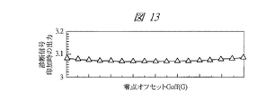
本実施の形態6における加速度センサは上記のように構成されており以下に初期診断時における動作について図10と図11を参照しながら説明する。図11は本実施の形態6における初期診断の流れを示すフローチャートである。まず、診断信号を可動部5に印加しない初期状態で診断を開始し、(S101)診断開始時における加速度センサの出力(物理量算出部PCUの出力)を異常判断部WDUで読み取り、零点オフセットGoffとして記憶部MUに記憶する(S102)。続いて、スイッチSW2を使用して診断信号印加用端子TE3から容量素子C3に診断信号を印加する。これにより、可動部5は+方向に変位する。この状態での加速度センサの出力(物理量算出部PCUの出力)を異常判断部WDUで読み取り、Gpとして記憶部MUに記憶する(S103)。次に、スイッチSW2を使用して診断信号印加用端子TE4から容量素子C4に診断信号を印加する。これにより、可動部5は−方向に変位する。この状態での加速度センサの出力(物理量算出部PCUの出力)を異常判断部WDUで読み取り、Gnとして記憶部MUに記憶する(S104)。なお、診断信号が診断信号印加用端子TE3に印加される場合、診断信号印加用端子TE4は、仮想接地(電圧変換部CVTのバイアス電圧104と接続)される。
The acceleration sensor according to the sixth embodiment is configured as described above, and the operation during the initial diagnosis will be described below with reference to FIGS. FIG. 11 is a flowchart showing a flow of initial diagnosis in the sixth embodiment. First, diagnosis is started in an initial state in which a diagnostic signal is not applied to the
続いて、演算部OUは、記憶部MUに記憶されているGpとGnの差分を計算してGspanを計算する(S105)。その後、比較部CPは、予め定められている既定範囲と演算部OUで計算されたGspanとを比較する(S106)。そして、判断部DUは、比較部CPでの比較結果に基づいて加速度センサの異常の有無を判断する。具体的に、判断部DUは、Gspanが既定範囲外にあるという比較結果を得た場合、加速度センサに異常があると判断する(S107)。一方、判断部DUは、Gspanが既定範囲内にあるという比較結果を得た場合、加速度センサが正常であると判断する(S108)。このようにして初期診断を終了する(S109)。 Subsequently, the arithmetic unit OU calculates Gspan by calculating the difference between Gp and Gn stored in the storage unit MU (S105). Thereafter, the comparison unit CP compares a predetermined range determined in advance with the Gspan calculated by the calculation unit OU (S106). Then, the determination unit DU determines whether the acceleration sensor is abnormal based on the comparison result in the comparison unit CP. Specifically, the determination unit DU determines that there is an abnormality in the acceleration sensor when obtaining a comparison result that Gspan is outside the predetermined range (S107). On the other hand, the determination unit DU determines that the acceleration sensor is normal when obtaining a comparison result that Gspan is within the predetermined range (S108). In this way, the initial diagnosis is completed (S109).
次に既定範囲の設定について説明する。図12は、零点オフセットGoffと診断信号印加時の出力との関係を示すグラフである。横軸が零点オフセットを示しており、縦軸が診断信号印加時の出力を示している。図12において、三角印の曲線はGspanを示している。また、四角印の曲線がGpを示し、丸印の曲線がGn(実際の値は表示の値に−1を掛けた値)を示している。また、図13は、Gspanが描画されている領域を拡大したグラフである。 Next, the setting of the default range will be described. FIG. 12 is a graph showing the relationship between the zero offset Goff and the output when the diagnostic signal is applied. The horizontal axis indicates the zero point offset, and the vertical axis indicates the output when the diagnostic signal is applied. In FIG. 12, the triangular curve indicates Gspan. Further, the square curve indicates Gp, and the circle curve indicates Gn (the actual value is a value obtained by multiplying the displayed value by -1). FIG. 13 is an enlarged graph of a region where Gspan is drawn.
図12において、零点オフセットGoffが0の場合、GpとGnは1.525となっており、加速度センサの最大測定範囲(フールスケール)±1.5の診断を行なうため、
GpとGnは1.5よりも大きな値となっている。したがって、加速度センサに故障がなく、かつ、零点オフセットも0の状態(理想的に平坦な状態に置かれている状態)でのGspanは3.05となる。そして、図12および図13に示すように、零点オフセットが存在する場合、GpとGnが非線形的に変化し、Gspanの値がすべて3.05以上であることがわかる。本実施の形態6では、平行平板型の容量素子C3および容量素子C4の非線形的な性質を使用して診断を行なっている。つまり、図12および図13に示すように、零点オフセットが発生している場合、Gspanは零点オフセットが0の場合よりも必ず大きくなる。一方、可動部5が固着して動かない場合や電極間に異物が挟まって可動部5の変位が制限される場合、変位範囲が制限されることから、Gspanは3.05より小さくなる。したがって、加速度センサの異常による変位異常と、零点オフセットによる変位とは、零点オフセットが0の場合のGspanの値(3.05)を境に分離することができることがわかる。本実施の形態6では、この特徴を利用して、加速度センサの異常と零点オフセットとを区別しているのである。また、加速度センサの梁4が破損して可動部5が正常状態より動きやすくなる場合は、Gspanが異常に大きくなることから、Gspanに上限値(例えば、3.15(図11参照))を設けることにより、この異常を検出することができる。以上のことから、本実施の形態6では、Gspanに対して既定範囲を設定し、この既定範囲から外れている場合だけを異常と診断することにより、加速度センサが正常状態で、かつ、零点オフセットが発生している状態を異常であると誤診断することを抑制できる。
In FIG. 12, when zero offset Goff is 0, Gp and Gn are 1.525, and in order to perform diagnosis of the maximum measurement range (full scale) ± 1.5 of the acceleration sensor,
Gp and Gn are larger than 1.5. Therefore, Gspan is 3.05 when there is no failure in the acceleration sensor and the zero offset is zero (ideally placed in a flat state). As shown in FIG. 12 and FIG. 13, it can be seen that when there is a zero offset, Gp and Gn change nonlinearly, and the values of Gspan are all 3.05 or more. In the sixth embodiment, diagnosis is performed using the non-linear properties of the parallel plate type capacitive element C3 and the capacitive element C4. That is, as shown in FIGS. 12 and 13, when a zero offset occurs, Gspan is always larger than when the zero offset is zero. On the other hand, when the
次に、平行平板型の容量素子C3および容量素子C4が非線形的な性質を有するメカニズムについて説明する。図14は、可動部5に形成されている容量素子C1〜C4の構造を示している。容量素子C1と容量素子C2は、容量検出部を構成し、容量素子C3と容量素子C4は強制変位生成部を構成している。本実施の形態6のように容量素子C3および容量素子C4を使用して強制変位を生じさせるためには、非対称な電極構造とする必要がある。本実施の形態6の場合、強制変位生成部を構成する容量素子C3および容量素子C4は、平行平板型の電極構成となっており、1:3(d:3d)のギャップ比をもつように形成されている。例えば、1:1のギャップ比をもつように容量素子C3を構成すると、静電力Fpoと静電力Fpiが釣り合ってしまい可動部5を変位させることができなくなってしまうからである。
Next, a mechanism in which the parallel plate type capacitive element C3 and the capacitive element C4 have nonlinear properties will be described. FIG. 14 shows the structure of the capacitive elements C <b> 1 to C <b> 4 formed in the
診断信号によって可動部5に印加される静電力は式1〜式3および式4〜式6に示される。式1〜式3は、容量素子C3に印加される静電力を示しており、式4〜式6は、容量素子C4に印加される静電力を示している。
The electrostatic force applied to the
Fpo=1/2×εA/(d−y)2×Vdiag2 ・・・(1)
Fpi=1/2×εA/(3d+y)2×Vdiag2 ・・・(2)
Fp=Fpo−Fpi ・・・(3)
Fno=1/2×εA/(d+y)2×Vdiag2 ・・・(4)
Fni=1/2×εA/(3d−y)2×Vdiag2 ・・・(5)
Fn=Fno−Fni ・・・(6)
ここで、εは空気の誘電率、Aは電極の対向面積、dは電極間ギャップ、yは可動部5の零点オフセットによる変位量、Vdiagは診断信号の電圧を示している。
Fpo = 1/2 × εA / (dy) 2 × Vdiag 2 (1)
Fpi = 1/2 × εA / (3d + y) 2 × Vdiag 2 (2)
Fp = Fpo−Fpi (3)
Fno = 1/2 × εA / (d + y) 2 × Vdiag 2 (4)
Fni = 1/2 × εA / (3d−y) 2 × Vdiag 2 (5)
Fn = Fno−Fni (6)
Here, ε is the dielectric constant of air, A is the facing area of the electrodes, d is the gap between the electrodes, y is the amount of displacement due to the zero offset of the
以上の式1〜式6により、平行平板型の電極構造の場合、零点オフセットが式1〜式6中の分母にあるyに影響を及ぼすため、零点オフセットが変化すると、静電力Fpおよび静電力Fnが非線形的に変化することがわかる。
According to the
さらに、静電力Fpおよび静電力Fnは、図14の梁4のバネ定数をkとし、零点オフセットGoffを加算すれば式(7)で示される初期診断時の加速度センサの出力を得ることができる。 Furthermore, as for the electrostatic force Fp and the electrostatic force Fn, if the spring constant of the beam 4 in FIG. 14 is set to k and the zero point offset Goff is added, the output of the acceleration sensor at the initial diagnosis represented by the equation (7) can be obtained. .
Gp=Fp/k+Goff、Gn=Fn/k+Goff ・・・(7)
上述したGpとGnの結果を使用して加速度センサの故障の有無を判断する1つの指標をつくるため、GpとGnの差分をとることにより。式(8)で示されるGspanが得られる。
Gp = Fp / k + Goff, Gn = Fn / k + Goff (7)
By taking the difference between Gp and Gn in order to create one index for judging the presence or absence of a failure of the acceleration sensor using the results of Gp and Gn described above. Gspan represented by formula (8) is obtained.
Gspan=Gp−Gn=Fp/k+Goff−(Fn/k+Goff)
=Fp/k−Fn/k ・・・(8)
上述した図12のグラフは、式(1)〜式(8)を使用して、0から±0.8Gまでの零点オフセットを想定した場合におけるGp、Gn、Gspanの値である。つまり、加速度センサに異常(故障)がない場合、いかなる零点オフセットGoffに対しても、Gspanの値は、零点オフセットGoffが0である場合のGspanの値(3.05)よりも大きくなる。これを判断基準とすれば、加速度センサの異常の有無を判断することができるのである。
Gspan = Gp−Gn = Fp / k + Goff− (Fn / k + Goff)
= Fp / k-Fn / k (8)
The graph of FIG. 12 described above is the values of Gp, Gn, and Gspan when a zero point offset from 0 to ± 0.8 G is assumed using Equations (1) to (8). That is, when there is no abnormality (failure) in the acceleration sensor, the value of Gspan is greater than the value of Gspan (3.05) when the zero point offset Goff is 0 for any zero point offset Goff. If this is used as a criterion, it can be determined whether the acceleration sensor is abnormal.
例えば、可動部5が固着して動かない場合や、容量素子C1〜容量素子C4を構成する電極間に異物が挟まって可動部5の変位が制限される場合、Gspanの値は3.05よりも小さくなり、加速度センサが異常であると診断することができる。また、加速度センサの出力に影響を及ぼすほどの電気的なリークが容量素子C1〜容量素子C4に発生した場合でもGspanは3.05以下となるため、加速度センサが異常であると診断することができる。一方、梁4が破損して可動部5が正常状態よりも動きやすくなった場合、Gspanの値が設定されている既定範囲を超えるため、異常であると診断することができる。これに対し、零点オフセットGoffによって可動部5が変位する場合、Gspanは3.05より大きく既定範囲に入ることになる。したがって、加速度センサの異常による変位異常と、零点オフセットによる変位とは、零点オフセットが0の場合のGspanの値(3.05)を境に分離することができることがわかる。以上のことから、本実施の形態6では、Gspanに対して既定範囲を設定し、この既定範囲から外れている場合だけを異常と診断することにより、加速度センサが正常状態で、かつ、零点オフセットが発生している状態を異常であると誤診断することを抑制できることがわかる。
For example, when the
なお、図12のグラフからわかるように、想定する零点オフセットGoffの大きさに応じて加速度センサの測定範囲を広げる必要がある。例えば、本実施の形態6における加速度センサの場合、センサ出力としては最大±1.5Gの測定範囲であるが、零点オフセットGoffを±0.8Gまで想定すると、加速度センサの内部的には約±2.5Gまで測定できるように設計する必要がある。 As can be seen from the graph of FIG. 12, it is necessary to widen the measurement range of the acceleration sensor in accordance with the assumed zero offset Goff. For example, in the case of the acceleration sensor according to the sixth embodiment, the sensor output has a maximum measurement range of ± 1.5 G. However, assuming that the zero point offset Goff is ± 0.8 G, the acceleration sensor internally has about ± It is necessary to design so that it can measure up to 2.5G.
以上、本発明者によってなされた発明をその実施の形態に基づき具体的に説明したが、本発明は前記実施の形態に限定されるものではなく、その要旨を逸脱しない範囲で種々変更可能であることは言うまでもない。 As mentioned above, the invention made by the present inventor has been specifically described based on the embodiment. However, the invention is not limited to the embodiment, and various modifications can be made without departing from the scope of the invention. Needless to say.
本発明は、主に加速度センサに代表される静電容量式センサに利用することができる。特に、自動車の姿勢制御や介護ロボットの姿勢・動作制御などの高信頼性が要求される静電容量式センサに幅広く利用することができる。 The present invention can be mainly used for a capacitance type sensor represented by an acceleration sensor. In particular, it can be widely used for capacitive sensors that require high reliability, such as attitude control of automobiles and attitude / motion control of nursing robots.
1 枠部
1S 基板層
2 空洞部
3 固定部
3a パッド
4 梁
5 可動部
6a 検出用可動電極
6b 検出用固定電極
6c 検出用固定電極
7a パッド
7b パッド
8a 診断用可動電極
8b 診断用固定電極
8c 診断用固定電極
9a パッド
9b パッド
10 外枠体
11 接着材
12a パッド
12b パッド
13 接着材
14a ワイヤ
14b ワイヤ
15 リッド
20 振動体
21 角速度信号処理部
22 分周器
23 駆動部
24 搬送波生成部
100 診断信号
101 バイアス電圧
102 変調信号
103 バイアス電圧
104 バイアス電圧
105 駆動信号
106 搬送波
107 診断信号生成部
ADT A/D変換部
BOX 埋め込み絶縁層
Cf1 参照容量
Cf2 参照容量
CHP1 半導体チップ
CHP2 半導体チップ
CHP3 半導体チップ
CP 比較部
CU 算出部
CVT 電圧変換部
C1 容量素子
C2 容量素子
C3 容量素子
C4 容量素子
DSG 診断信号生成部
DU 判断部
FDU 第1同期検波部
Fni 静電力
Fno 静電力
Fpi 静電力
Fpo 静電力
HPF1 ハイパスフィルタ
HPF2 ハイパスフィルタ
LPF1 ローパスフィルタ
LPF2 ローパスフィルタ
MSG 変調信号生成部
MU 記憶部
OP1 オペアンプ
OP2 オペアンプ
OP3 オペアンプ
OU 演算部
PCU 物理量算出部
SDU 第2同期検波部
SW1 スイッチ
TE1 物理量算出端子
TE2 物理量算出端子
TE3 診断信号印加用端子
TE4 診断信号印加用端子
TE5 変調信号印加用端子
WDU 異常判断部
DESCRIPTION OF SYMBOLS 1 Frame part 1S Substrate layer 2 Cavity part 3 Fixed part 3a Pad 4 Beam 5 Movable part 6a Detection movable electrode 6b Detection fixed electrode 6c Detection fixed electrode 7a Pad 7b Pad 8a Diagnostic movable electrode 8b Diagnostic fixed electrode 8c Diagnosis Fixed electrode 9a Pad 9b Pad 10 Outer frame body 11 Adhesive material 12a Pad 12b Pad 13 Adhesive material 14a Wire 14b Wire 15 Lid 20 Vibrating body 21 Angular velocity signal processing unit 22 Divider 23 Drive unit 24 Carrier wave generating unit 100 Diagnostic signal 101 Bias voltage 102 Modulated signal 103 Bias voltage 104 Bias voltage 105 Drive signal 106 Carrier wave 107 Diagnostic signal generator ADT A / D converter BOX Embedded insulating layer Cf1 Reference capacitor Cf2 Reference capacitor CHP1 Semiconductor chip CHP2 Semiconductor chip CHP3 Semiconductor chip CP comparison unit CU calculation unit CVT voltage conversion unit C1 capacitive element C2 capacitive element C3 capacitive element C4 capacitive element DSG diagnostic signal generation unit DU judgment unit FDU first synchronous detection unit Fni electrostatic force Fno electrostatic force Fpi electrostatic force Fpo electrostatic force HPF1 High-pass filter HPF2 High-pass filter LPF1 Low-pass filter LPF2 Low-pass filter MSG Modulation signal generation unit MU Storage unit OP1 Operational amplifier OP2 Operational amplifier OP3 Operational amplifier OU Operation unit PCU Physical quantity calculation unit SDU Second synchronous detection unit SW1 Switch TE1 Physical quantity calculation terminal TE2 Physical quantity calculation terminal TE2 Signal application terminal TE4 Diagnostic signal application terminal TE5 Modulation signal application terminal WDU Abnormality judgment unit
Claims (19)
(b)前記基板に形成された空洞部と、
(c)前記空洞部内に形成された固定部と、
(d)前記空洞部内に形成され、前記固定部と接続された弾性変形部と、
(e)前記空洞部内に形成され、前記弾性変形部と接続された可動部と、
(f)前記空洞部内に形成された第1固定電極と、前記可動部に形成された第1可動電極とを互いに対向させた第1容量素子を含み、前記可動部が変位することで生じる前記第1容量素子の容量変化を出力する容量検出部と、
(g)前記容量検出部から出力された容量変化に基づいて外力の物理量を求める物理量算出部と接続される物理量算出端子と、
(h)前記空洞部内に形成された第2固定電極と、前記可動部に形成された第2可動電極とを互いに対向させた第2容量素子を含み、かつ、前記第2固定電極と前記第2可動電極の間に診断信号を印加するための診断信号印加用端子とを含み、前記診断信号印加用端子に診断信号を印加することにより、前記第2固定電極と前記第2可動電極の間に静電気力を発生させて強制振動させる強制振動生成部と、
(i)前記強制振動生成部で発生した強制振動に基づいて、静電容量式センサの異常の有無を判断する異常判断部と間接的に接続される前記物理量算出端子とを備え、
前記容量検出部に含まれる前記第1容量素子と、前記強制振動生成部に含まれる前記第2容量素子とは分離され、
前記可動部の強制振動による加振周波数は、前記外力による前記可動部の変位に基づく外力応答周波数よりも高く、
前記物理量算出部は、
(j1)前記容量検出部から出力された容量変化を電圧信号に変換する電圧変換部と、
(j2)前記電圧変換部から出力された電圧信号から前記加振周波数と前記外力応答周波数を含む第1特定帯域の信号を抽出する第1同期検波部と、
(j3)前記第1同期検波部で抽出された前記第1特定帯域の信号から前記外力応答周波数の信号を抽出する第1低帯域通過フィルタと、
(j4)前記第1低帯域通過フィルタを通過した前記外力応答周波数の信号から前記外力の前記物理量を算出する算出部とを有し、
前記異常判断部は、
(l1)前記第1同期検波部で抽出された前記第1特定帯域の信号を入力し、入力した前記第1特定帯域の信号から前記加振周波数の信号に対応した第1検波周波数の信号と、前記第1検波周波数よりも高く、前記加振周波数の信号に対応した第2検波周波数の信号とを抽出する第2同期検波部と、
(l2)前記第2同期検波部で抽出された前記第1検波周波数の信号と前記第2検波周波数の信号のうち、前記第1検波周波数の信号を通過させる第2低帯域通過フィルタと、
(l3)前記第2低帯域通過フィルタを通過した前記第1検波周波数の信号と、予め定められている既定値とを比較する比較部と、
(l4)前記比較部の結果に基づいて、静電容量式センサの異常の有無を判断する判断部とを有することを特徴とする静電容量式センサ。 (A) a substrate;
(B) a cavity formed in the substrate;
(C) a fixing part formed in the cavity part;
(D) an elastically deformable portion formed in the hollow portion and connected to the fixed portion;
(E) a movable part formed in the cavity and connected to the elastic deformation part;
(F) including a first capacitor element in which a first fixed electrode formed in the hollow portion and a first movable electrode formed in the movable portion are opposed to each other, and is generated when the movable portion is displaced. A capacitance detection unit that outputs a capacitance change of the first capacitance element;
(G) a physical quantity calculation terminal connected to a physical quantity calculation unit for obtaining a physical quantity of an external force based on a change in capacity output from the capacity detection unit;
(H) including a second capacitor element in which the second fixed electrode formed in the cavity and the second movable electrode formed in the movable part are opposed to each other, and the second fixed electrode and the first A diagnostic signal application terminal for applying a diagnostic signal between the two movable electrodes, and applying a diagnostic signal to the diagnostic signal application terminal to thereby provide a gap between the second fixed electrode and the second movable electrode. A forced vibration generator that generates electrostatic force and forcibly vibrates,
(I) the physical quantity calculation terminal indirectly connected to an abnormality determination unit that determines whether there is an abnormality in the capacitance type sensor based on the forced vibration generated in the forced vibration generation unit;
The first capacitance element included in the capacitance detection unit and the second capacitance element included in the forced vibration generation unit are separated,
The vibration frequency caused by the forced oscillation of the movable portion, rather higher than the external force response frequency based on the displacement of the movable portion by the external force,
The physical quantity calculation unit
(J1) a voltage conversion unit that converts a capacitance change output from the capacitance detection unit into a voltage signal;
(J2) a first synchronous detection unit that extracts a signal in a first specific band including the excitation frequency and the external force response frequency from the voltage signal output from the voltage conversion unit;
(J3) a first low-pass filter that extracts a signal of the external force response frequency from the signal of the first specific band extracted by the first synchronous detector;
(J4) a calculation unit that calculates the physical quantity of the external force from the signal of the external force response frequency that has passed through the first low-pass filter,
The abnormality determination unit
(L1) The first specific band signal extracted by the first synchronous detection unit is input, and the first detection frequency signal corresponding to the excitation frequency signal from the input first specific band signal; A second synchronous detection unit that extracts a signal having a second detection frequency higher than the first detection frequency and corresponding to the signal having the excitation frequency;
(L2) Of the first detection frequency signal and the second detection frequency signal extracted by the second synchronous detection unit, a second low-pass filter that passes the first detection frequency signal;
(L3) a comparison unit that compares the signal of the first detection frequency that has passed through the second low-pass filter with a predetermined value;
(14) A capacitance sensor, comprising: a determination unit that determines whether there is an abnormality in the capacitance sensor based on the result of the comparison unit .
(b)前記基板に形成された空洞部と、(B) a cavity formed in the substrate;
(c)前記空洞部内に形成された固定部と、(C) a fixing part formed in the cavity part;
(d)前記空洞部内に形成され、前記固定部と接続された弾性変形部と、(D) an elastically deformable portion formed in the hollow portion and connected to the fixed portion;
(e)前記空洞部内に形成され、前記弾性変形部と接続された可動部と、(E) a movable part formed in the cavity and connected to the elastic deformation part;
(f)前記空洞部内に形成された第1固定電極と、前記可動部に形成された第1可動電極とを互いに対向させた第1容量素子を含み、前記可動部が変位することで生じる前記第1容量素子の容量変化を出力する容量検出部と、(F) including a first capacitor element in which a first fixed electrode formed in the hollow portion and a first movable electrode formed in the movable portion are opposed to each other, and is generated when the movable portion is displaced. A capacitance detection unit that outputs a capacitance change of the first capacitance element;
(g)前記容量検出部から出力された容量変化に基づいて外力の物理量を求める物理量算出部と接続される物理量算出端子と、(G) a physical quantity calculation terminal connected to a physical quantity calculation unit for obtaining a physical quantity of an external force based on a change in capacity output from the capacity detection unit;
(h)前記空洞部内に形成された第2固定電極と、前記可動部に形成された第2可動電極とを互いに対向させた第2容量素子を含み、かつ、前記第2固定電極と前記第2可動電極の間に診断信号を印加するための診断信号印加用端子とを含み、前記診断信号印加用端子に診断信号を印加することにより、前記第2固定電極と前記第2可動電極の間に静電気力を発生させて強制振動させる強制振動生成部と、(H) including a second capacitor element in which the second fixed electrode formed in the cavity and the second movable electrode formed in the movable part are opposed to each other, and the second fixed electrode and the first A diagnostic signal application terminal for applying a diagnostic signal between the two movable electrodes, and applying a diagnostic signal to the diagnostic signal application terminal to thereby provide a gap between the second fixed electrode and the second movable electrode. A forced vibration generator that generates electrostatic force and forcibly vibrates,
(i)前記強制振動生成部で発生した強制振動に基づいて、静電容量式センサの異常の有無を判断する異常判断部と間接的に接続される前記物理量算出端子とを備え、(I) the physical quantity calculation terminal indirectly connected to an abnormality determination unit that determines whether there is an abnormality in the capacitance type sensor based on the forced vibration generated in the forced vibration generation unit;
前記容量検出部に含まれる前記第1容量素子と、前記強制振動生成部に含まれる前記第2容量素子とは分離され、The first capacitance element included in the capacitance detection unit and the second capacitance element included in the forced vibration generation unit are separated,
前記可動部の強制振動による加振周波数は、前記外力による前記可動部の変位に基づく外力応答周波数よりも高く、The excitation frequency due to the forced vibration of the movable part is higher than the external force response frequency based on the displacement of the movable part due to the external force,
前記物理量算出部は、The physical quantity calculation unit
(j1)前記容量検出部から出力された容量変化を電圧信号に変換する電圧変換部と、(J1) a voltage conversion unit that converts a capacitance change output from the capacitance detection unit into a voltage signal;
(j2)前記電圧変換部から出力された電圧信号から前記加振周波数と前記外力応答周波数を含む第1特定帯域の信号を抽出する第1同期検波部と、(J2) a first synchronous detection unit that extracts a signal in a first specific band including the excitation frequency and the external force response frequency from the voltage signal output from the voltage conversion unit;
(j3)前記第1同期検波部で抽出された前記第1特定帯域の信号から前記外力応答周波数の信号を抽出する第1低帯域通過フィルタと、(J3) a first low-pass filter that extracts a signal of the external force response frequency from the signal of the first specific band extracted by the first synchronous detector;
(j4)前記第1低帯域通過フィルタを通過した前記外力応答周波数の信号から前記外力の前記物理量を算出する算出部とを有し、(J4) a calculation unit that calculates the physical quantity of the external force from the signal of the external force response frequency that has passed through the first low-pass filter,
前記異常判断部は、The abnormality determination unit
(l1)前記第1同期検波部で抽出された前記第1特定帯域の信号を入力し、入力した前記第1特定帯域の信号から前記加振周波数の信号に対応した第1検波周波数の信号と、前記第1検波周波数よりも高く、前記加振周波数の信号に対応した第2検波周波数の信号とを抽出する第2同期検波部と、(L1) The first specific band signal extracted by the first synchronous detection unit is input, and the first detection frequency signal corresponding to the excitation frequency signal from the input first specific band signal; A second synchronous detection unit that extracts a signal having a second detection frequency higher than the first detection frequency and corresponding to the signal having the excitation frequency;
(l2)前記第2同期検波部で抽出された前記第1検波周波数の信号と前記第2検波周波数の信号のうち、前記第2検波周波数の信号を通過させる第2高帯域通過フィルタと、(L2) Of the first detection frequency signal and the second detection frequency signal extracted by the second synchronous detection unit, a second high-pass filter that passes the second detection frequency signal;
(l3)前記第2高帯域通過フィルタを通過した前記第2検波周波数の信号と、予め定められている既定値とを比較する比較部と、(L3) a comparison unit that compares the signal of the second detection frequency that has passed through the second high-pass filter with a predetermined value;
(l4)前記比較部の結果に基づいて、静電容量式センサの異常の有無を判断する判断部とを有することを特徴とする静電容量式センサ。(14) A capacitance sensor, comprising: a determination unit that determines whether there is an abnormality in the capacitance sensor based on the result of the comparison unit.
(j)前記物理量算出端子と接続される前記物理量算出部と、
(k)前記診断信号を生成し、前記診断信号印加用端子と接続される診断信号生成部と、
(l)前記物理量算出端子と間接的に接続される前記異常判断部とを有することを特徴とする静電容量式センサ。 The capacitance sensor of claim 1 or 2, further comprising:
(J) the physical quantity calculation unit connected to the physical quantity calculation terminal;
(K) a diagnostic signal generator that generates the diagnostic signal and is connected to the diagnostic signal application terminal;
(L) The capacitance type sensor having the abnormality determination unit indirectly connected to the physical quantity calculation terminal.
(m)前記可動部に変調信号を印加するための変調信号印加用端子と、
(n)前記変調信号を生成し、前記変調信号印加用端子と接続された変調信号生成部とを有することを特徴とする静電容量式センサ。 The capacitive sensor according to claim 3 , further comprising:
(M) a modulation signal applying terminal for applying a modulation signal to the movable part;
(N) A capacitance type sensor that includes the modulation signal generation unit that generates the modulation signal and is connected to the modulation signal application terminal.
前記第1容量素子の容量変化は、前記外力による前記可動部の変位に起因する第1容量変化と、前記強制振動生成部による前記可動部の強制振動に起因する第2容量変化が含まれていることを特徴とする静電容量式センサ。 The capacitive sensor according to claim 4 , wherein
The capacitance change of the first capacitive element includes a first capacitance change caused by displacement of the movable part due to the external force and a second capacitance change caused by forced vibration of the movable part caused by the forced vibration generation part. A capacitive sensor characterized by comprising:
前記可動部の強制振動による前記加振周波数は、前記変調信号の搬送波周波数よりも低いことを特徴とする静電容量式センサ。 The capacitive sensor according to claim 5 , wherein
The vibration frequency caused by the forced oscillation of the movable portion, the electrostatic capacitance type sensor being lower than the carrier frequency of the modulated signal.
前記異常判断部は、さらに、前記第2同期検波部の前に、前記第1特定帯域の信号を入力し、入力した前記第1特定帯域の信号のうち、前記外力応答周波数よりも高い帯域の信号を通過させる第1高帯域通過フィルタを有することを特徴とする静電容量式センサ。 The capacitive sensor according to claim 1 ,
The abnormality determination unit further inputs a signal of the first specific band before the second synchronous detection unit, and has a band higher than the external force response frequency among the input signals of the first specific band. A capacitance type sensor having a first high-band pass filter for passing a signal.
前記異常判断部は、さらに、前記第2同期検波部の前に、前記第1特定帯域の信号を入力し、入力した前記第1特定帯域の信号のうち、前記外力応答周波数よりも高い帯域の信号を通過させる第1高帯域通過フィルタを有することを特徴とする静電容量式センサ。 The capacitive sensor according to claim 2 , wherein
The abnormality determination unit further inputs a signal of the first specific band before the second synchronous detection unit, and has a band higher than the external force response frequency among the input signals of the first specific band. A capacitance type sensor having a first high-band pass filter for passing a signal.
(j)前記物理量算出端子と接続される前記物理量算出部と、
(k)前記診断信号を生成し、前記診断信号印加用端子と接続される診断信号生成部と、
(l)前記物理量算出端子と間接的に接続される前記異常判断部とを有し、
前記診断信号生成部と前記診断信号印加用端子との間にスイッチを有し、
前記異常判断部は、前記スイッチを周期的にオン/オフし、
前記比較部は、さらに、オン時の前記第1検波周波数の信号とオフ時の前記第1検波周波数の信号との差分値を算出し、
前記判断部は、さらに、前記差分値に基づいて、静電容量式センサの異常の有無を判断することを特徴とする静電容量式センサ。 The capacitive sensor according to claim 1 , further comprising:
(J) the physical quantity calculation unit connected to the physical quantity calculation terminal;
(K) a diagnostic signal generator that generates the diagnostic signal and is connected to the diagnostic signal application terminal;
(L) having the abnormality determination unit indirectly connected to the physical quantity calculation terminal;
A switch between the diagnostic signal generator and the diagnostic signal application terminal;
The abnormality determining unit periodically turns on / off the switch,
The comparison unit further calculates a difference value between the signal at the first detection frequency when on and the signal at the first detection frequency when off.
The determination unit further determines presence / absence of abnormality of the capacitance type sensor based on the difference value.
(j)前記物理量算出端子と接続される前記物理量算出部と、
(k)前記診断信号を生成し、前記診断信号印加用端子と接続される診断信号生成部と、
(l)前記物理量算出端子と間接的に接続される前記異常判断部とを有し、
前記診断信号生成部と前記診断信号印加用端子との間にスイッチを有し、
前記異常判断部は、前記スイッチを周期的にオン/オフし、
前記比較部は、さらに、オン時の前記第2検波周波数の信号とオフ時の前記第2検波周波数の信号との差分値を算出し、
前記判断部は、さらに、前記差分値に基づいて、静電容量式センサの異常の有無を判断することを特徴とする静電容量式センサ。 The capacitive sensor according to claim 2 , further comprising:
(J) the physical quantity calculation unit connected to the physical quantity calculation terminal;
(K) a diagnostic signal generator that generates the diagnostic signal and is connected to the diagnostic signal application terminal;
(L) having the abnormality determination unit indirectly connected to the physical quantity calculation terminal;
A switch between the diagnostic signal generator and the diagnostic signal application terminal;
The abnormality determining unit periodically turns on / off the switch,
The comparison unit further calculates a difference value between the signal at the second detection frequency when on and the signal at the second detection frequency when off.
The determination unit further determines presence / absence of abnormality of the capacitance type sensor based on the difference value.
前記外力の物理量は加速度であることを特徴とする静電容量式センサ。 The capacitive sensor according to claim 6 , wherein
The capacitance type sensor is characterized in that the physical quantity of the external force is acceleration.
さらに、角速度センサを構成する構造体が形成されており、
前記構造体は、動作時に振動させている振動体と、前記振動体を特定周波数で振動させる駆動部とを含むことを特徴とする静電容量式センサ。 The capacitive sensor according to claim 11 , wherein
Furthermore, a structure constituting the angular velocity sensor is formed,
The structure body includes a vibrating body that vibrates during operation, and a drive unit that vibrates the vibrating body at a specific frequency.
加速度センサの前記可動部を強制振動させている前記加振周波数は、前記特定周波数の2のべき乗分の1の周波数であることを特徴とする静電容量式センサ。 The capacitive sensor according to claim 12 , wherein
The capacitive sensor, wherein the excitation frequency for forcibly vibrating the movable part of the acceleration sensor is a frequency that is a power of 2 of the specific frequency.
前記診断信号生成部と前記診断信号印加用端子との間にスイッチを有し、
前記異常判断部は、前記スイッチのオン/オフを、前記特定周波数の2のべき乗分の1の周波数で制御していることを特徴とする静電容量式センサ。 The capacitive sensor according to claim 12 , wherein
A switch between the diagnostic signal generator and the diagnostic signal application terminal;
The abnormality determination unit controls on / off of the switch at a frequency that is a power of 2 of the specific frequency.
(b)前記基板に形成された空洞部と、
(c)前記空洞部内に形成された固定部と、
(d)前記空洞部内に形成され、前記固定部と接続された弾性変形部と、
(e)前記空洞部内に形成され、前記弾性変形部と接続された可動部と、
(f)前記空洞部内に形成された第1固定電極と、前記可動部に形成された第1可動電極とを互いに対向させた第1容量素子を含み、前記可動部が変位することで生じる前記第1容量素子の容量変化を出力する容量検出部と、
(g)前記容量検出部から出力された容量変化に基づいて外力の物理量を求める物理量算出部と接続される物理量算出端子と、
(h)前記空洞部内に形成された第2固定電極と、前記可動部に形成された第2可動電極とを互いに対向させた第2容量素子とを含み、かつ、前記第2固定電極と前記第2可動電極の間に第1診断信号を印加するための第1診断信号印加用端子と、前記第2固定電極と前記第2可動電極の間に第2診断信号を印加するための第2診断信号印加用端子とを含み、動作開始時、前記第1診断信号印加用端子に前記第1診断信号を印加することにより、前記可動部を第1方向へ変位させ、前記第2診断信号印加用端子に前記第2診断信号を印加することにより、前記可動部を前記第1方向とは反対側の第2方向へ変位させる強制変位生成部と、
(i)前記強制変位生成部で発生した強制変位に基づいて、静電容量式センサの異常の有無を判断する異常判断部と間接的に接続される前記物理量算出端子とを備え、
前記容量検出部に含まれる前記第1容量素子と、前記強制変位生成部に含まれる前記第2容量素子とは分離され、
前記異常判断部は、
(l1)動作開始時、前記物理量算出部から入力した初期オフセット値と、前記第1診断信号印加用端子に前記第1診断信号を印加することにより、前記可動部を前記第1方向へ変位させたとき、前記物理量算出部から入力した第1入力値と、前記第2診断信号印加用端子に前記第2診断信号を印加することにより、前記可動部を前記第2方向へ変位させたとき、前記物理量算出部から入力した第2入力値とを記憶する記憶部と、
(l2)前記記憶部に記憶されている前記第1入力値と前記第2入力値の差分値を算出する演算部と、
(l3)前記演算部で算出された前記差分値と予め設定されている既定範囲値とを比較する比較部と、
(l4)前記比較部の結果に基づいて、静電容量式センサの異常の有無を判断する判断部とを有することを特徴とする静電容量式センサ。 (A) a substrate;
(B) a cavity formed in the substrate;
(C) a fixing part formed in the cavity part;
(D) an elastically deformable portion formed in the hollow portion and connected to the fixed portion;
(E) a movable part formed in the cavity and connected to the elastic deformation part;
(F) including a first capacitor element in which a first fixed electrode formed in the hollow portion and a first movable electrode formed in the movable portion are opposed to each other, and is generated when the movable portion is displaced. A capacitance detection unit that outputs a capacitance change of the first capacitance element;
(G) a physical quantity calculation terminal connected to a physical quantity calculation unit for obtaining a physical quantity of an external force based on a change in capacity output from the capacity detection unit;
(H) including a second fixed electrode formed in the hollow portion and a second capacitor element in which the second movable electrode formed in the movable portion is opposed to each other, and the second fixed electrode and the A first diagnostic signal applying terminal for applying a first diagnostic signal between the second movable electrodes; and a second for applying a second diagnostic signal between the second fixed electrode and the second movable electrode. A diagnostic signal application terminal, and at the start of operation, by applying the first diagnostic signal to the first diagnostic signal application terminal, the movable part is displaced in the first direction, and the second diagnostic signal application By applying the second diagnostic signal to the terminal for use, to displace the movable part in the second direction opposite to the first direction;
(I) the physical quantity calculation terminal indirectly connected to an abnormality determination unit that determines whether there is an abnormality in the capacitance type sensor based on the forced displacement generated in the forced displacement generation unit;
The first capacitance element included in the capacitance detection unit and the second capacitance element included in the forced displacement generation unit are separated ,
The abnormality determination unit
(L1) At the start of operation, the movable part is displaced in the first direction by applying the initial offset value input from the physical quantity calculator and the first diagnostic signal to the first diagnostic signal application terminal. When the movable part is displaced in the second direction by applying the second diagnostic signal to the first input value input from the physical quantity calculation unit and the second diagnostic signal application terminal, A storage unit for storing the second input value input from the physical quantity calculation unit;
(L2) a calculation unit that calculates a difference value between the first input value and the second input value stored in the storage unit;
(L3) a comparison unit that compares the difference value calculated by the calculation unit with a preset default range value;
(14) A capacitance sensor, comprising: a determination unit that determines whether there is an abnormality in the capacitance sensor based on the result of the comparison unit .
(j)前記物理量算出端子と接続される前記物理量算出部と、
(k)前記第1診断信号あるいは前記第2診断信号を生成し、前記第1診断信号印加用端子あるいは前記第2診断信号印加用端子と接続される診断信号生成部と、
(l)前記物理量算出端子と間接的に接続される前記異常判断部とを有することを特徴とする静電容量式センサ。 The capacitive sensor according to claim 15 , further comprising:
(J) the physical quantity calculation unit connected to the physical quantity calculation terminal;
(K) a diagnostic signal generator that generates the first diagnostic signal or the second diagnostic signal and is connected to the first diagnostic signal application terminal or the second diagnostic signal application terminal;
(L) The capacitance type sensor having the abnormality determination unit indirectly connected to the physical quantity calculation terminal.
(b)前記基板に形成された空洞部と、
(c)前記空洞部内に形成された固定部と、
(d)前記空洞部内に形成され、前記固定部と接続された弾性変形部と、
(e)前記空洞部内に形成され、前記弾性変形部と接続された可動部と、
(f)前記空洞部内に形成された第1固定電極と、前記可動部に形成された第1可動電極とを互いに対向させた第1容量素子を含み、前記可動部が変位することで生じる前記第1容量素子の容量変化を出力する容量検出部と、
(g)前記容量検出部から出力された容量変化に基づいて外力の物理量を求める物理量算出部と、
(h)前記空洞部内に形成された第2固定電極と、前記可動部に形成された第2可動電極とを互いに対向させた第2容量素子を含み、かつ、前記第2固定電極と前記第2可動電極の間に診断信号を印加するための診断信号印加用端子とを含み、前記診断信号印加用端子に前記診断信号を印加することにより、前記第2固定電極と前記第2可動電極の間に静電気力を発生させて強制振動させる強制振動生成部と、
(i)前記強制振動生成部で発生した強制振動に基づいて、静電容量式センサの異常の有無を判断する異常判断部とを備え、
前記容量検出部に含まれる前記第1容量素子と、前記強制振動生成部に含まれる前記第2容量素子とは分離され、
前記可動部の強制振動による加振周波数は、前記外力による前記可動部の変位に基づく外力応答周波数よりも高く、
前記物理量算出部は、
(j1)前記容量検出部から出力された容量変化を電圧信号に変換する電圧変換部と、
(j2)前記電圧変換部から出力された電圧信号から前記加振周波数と前記外力応答周波数を含む第1特定帯域の信号を抽出する第1同期検波部と、
(j3)前記第1同期検波部で抽出された前記第1特定帯域の信号から前記外力応答周波数の信号を抽出する第1低帯域通過フィルタと、
(j4)前記第1低帯域通過フィルタを通過した前記外力応答周波数の信号から前記外力の前記物理量を算出する算出部とを有し、
前記異常判断部は、
(l1)前記第1同期検波部で抽出された前記第1特定帯域の信号を入力し、入力した前記第1特定帯域の信号から前記加振周波数の信号に対応した第1検波周波数の信号と、前記第1検波周波数よりも高く、前記加振周波数の信号に対応した第2検波周波数の信号とを抽出する第2同期検波部と、
(l2)前記第2同期検波部で抽出された前記第1検波周波数の信号と前記第2検波周波数の信号のうち、前記第1検波周波数の信号を通過させる第2低帯域通過フィルタと、
(l3)前記第2低帯域通過フィルタを通過した前記第1検波周波数の信号と、予め定められている既定値とを比較する比較部と、
(l4)前記比較部の結果に基づいて、静電容量式センサの異常の有無を判断する判断部とを有することを特徴とする静電容量式センサ。 (A) a substrate;
(B) a cavity formed in the substrate;
(C) a fixing part formed in the cavity part;
(D) an elastically deformable portion formed in the hollow portion and connected to the fixed portion;
(E) a movable part formed in the cavity and connected to the elastic deformation part;
(F) including a first capacitor element in which a first fixed electrode formed in the hollow portion and a first movable electrode formed in the movable portion are opposed to each other, and is generated when the movable portion is displaced. A capacitance detection unit that outputs a capacitance change of the first capacitance element;
(G) a physical quantity calculation unit for obtaining a physical quantity of external force based on a change in capacity output from the capacity detection unit;
(H) including a second capacitor element in which the second fixed electrode formed in the cavity and the second movable electrode formed in the movable part are opposed to each other, and the second fixed electrode and the first A diagnostic signal applying terminal for applying a diagnostic signal between the two movable electrodes, and applying the diagnostic signal to the diagnostic signal applying terminal allows the second fixed electrode and the second movable electrode to A forced vibration generator that generates electrostatic force between them to forcibly vibrate,
(I) an abnormality determination unit that determines whether there is an abnormality in the capacitance type sensor based on the forced vibration generated in the forced vibration generation unit;
The first capacitance element included in the capacitance detection unit and the second capacitance element included in the forced vibration generation unit are separated,
The vibration frequency caused by the forced oscillation of the movable portion, rather higher than the external force response frequency based on the displacement of the movable portion by the external force,
The physical quantity calculation unit
(J1) a voltage conversion unit that converts a capacitance change output from the capacitance detection unit into a voltage signal;
(J2) a first synchronous detection unit that extracts a signal in a first specific band including the excitation frequency and the external force response frequency from the voltage signal output from the voltage conversion unit;
(J3) a first low-pass filter that extracts a signal of the external force response frequency from the signal of the first specific band extracted by the first synchronous detector;
(J4) a calculation unit that calculates the physical quantity of the external force from the signal of the external force response frequency that has passed through the first low-pass filter,
The abnormality determination unit
(L1) The first specific band signal extracted by the first synchronous detection unit is input, and the first detection frequency signal corresponding to the excitation frequency signal from the input first specific band signal; A second synchronous detection unit that extracts a signal having a second detection frequency higher than the first detection frequency and corresponding to the signal having the excitation frequency;
(L2) Of the first detection frequency signal and the second detection frequency signal extracted by the second synchronous detection unit, a second low-pass filter that passes the first detection frequency signal;
(L3) a comparison unit that compares the signal of the first detection frequency that has passed through the second low-pass filter with a predetermined value;
(14) A capacitance sensor, comprising: a determination unit that determines whether there is an abnormality in the capacitance sensor based on the result of the comparison unit .
(b)前記基板に形成された空洞部と、(B) a cavity formed in the substrate;
(c)前記空洞部内に形成された固定部と、(C) a fixing part formed in the cavity part;
(d)前記空洞部内に形成され、前記固定部と接続された弾性変形部と、(D) an elastically deformable portion formed in the hollow portion and connected to the fixed portion;
(e)前記空洞部内に形成され、前記弾性変形部と接続された可動部と、(E) a movable part formed in the cavity and connected to the elastic deformation part;
(f)前記空洞部内に形成された第1固定電極と、前記可動部に形成された第1可動電極とを互いに対向させた第1容量素子を含み、前記可動部が変位することで生じる前記第1容量素子の容量変化を出力する容量検出部と、(F) including a first capacitor element in which a first fixed electrode formed in the hollow portion and a first movable electrode formed in the movable portion are opposed to each other, and is generated when the movable portion is displaced. A capacitance detection unit that outputs a capacitance change of the first capacitance element;
(g)前記容量検出部から出力された容量変化に基づいて外力の物理量を求める物理量算出部と、(G) a physical quantity calculation unit for obtaining a physical quantity of external force based on a change in capacity output from the capacity detection unit;
(h)前記空洞部内に形成された第2固定電極と、前記可動部に形成された第2可動電極とを互いに対向させた第2容量素子を含み、かつ、前記第2固定電極と前記第2可動電極の間に診断信号を印加するための診断信号印加用端子とを含み、前記診断信号印加用端子に前記診断信号を印加することにより、前記第2固定電極と前記第2可動電極の間に静電気力を発生させて強制振動させる強制振動生成部と、(H) including a second capacitor element in which the second fixed electrode formed in the cavity and the second movable electrode formed in the movable part are opposed to each other, and the second fixed electrode and the first A diagnostic signal applying terminal for applying a diagnostic signal between the two movable electrodes, and applying the diagnostic signal to the diagnostic signal applying terminal allows the second fixed electrode and the second movable electrode to A forced vibration generator that generates electrostatic force between them to forcibly vibrate,
(i)前記強制振動生成部で発生した強制振動に基づいて、静電容量式センサの異常の有無を判断する異常判断部とを備え、(I) an abnormality determination unit that determines whether there is an abnormality in the capacitance type sensor based on the forced vibration generated in the forced vibration generation unit;
前記容量検出部に含まれる前記第1容量素子と、前記強制振動生成部に含まれる前記第2容量素子とは分離され、The first capacitance element included in the capacitance detection unit and the second capacitance element included in the forced vibration generation unit are separated,
前記可動部の強制振動による加振周波数は、前記外力による前記可動部の変位に基づく外力応答周波数よりも高く、The excitation frequency due to the forced vibration of the movable part is higher than the external force response frequency based on the displacement of the movable part due to the external force,
前記物理量算出部は、The physical quantity calculation unit
(j1)前記容量検出部から出力された容量変化を電圧信号に変換する電圧変換部と、(J1) a voltage conversion unit that converts a capacitance change output from the capacitance detection unit into a voltage signal;
(j2)前記電圧変換部から出力された電圧信号から前記加振周波数と前記外力応答周波数を含む第1特定帯域の信号を抽出する第1同期検波部と、(J2) a first synchronous detection unit that extracts a signal in a first specific band including the excitation frequency and the external force response frequency from the voltage signal output from the voltage conversion unit;
(j3)前記第1同期検波部で抽出された前記第1特定帯域の信号から前記外力応答周波数の信号を抽出する第1低帯域通過フィルタと、(J3) a first low-pass filter that extracts a signal of the external force response frequency from the signal of the first specific band extracted by the first synchronous detector;
(j4)前記第1低帯域通過フィルタを通過した前記外力応答周波数の信号から前記外力の前記物理量を算出する算出部とを有し、(J4) a calculation unit that calculates the physical quantity of the external force from the signal of the external force response frequency that has passed through the first low-pass filter,
前記異常判断部は、The abnormality determination unit
(l1)前記第1同期検波部で抽出された前記第1特定帯域の信号を入力し、入力した前記第1特定帯域の信号から前記加振周波数の信号に対応した第1検波周波数の信号と、前記第1検波周波数よりも高く、前記加振周波数の信号に対応した第2検波周波数の信号とを抽出する第2同期検波部と、(L1) The first specific band signal extracted by the first synchronous detection unit is input, and the first detection frequency signal corresponding to the excitation frequency signal from the input first specific band signal; A second synchronous detection unit that extracts a signal having a second detection frequency higher than the first detection frequency and corresponding to the signal having the excitation frequency;
(l2)前記第2同期検波部で抽出された前記第1検波周波数の信号と前記第2検波周波数の信号のうち、前記第2検波周波数の信号を通過させる第2高帯域通過フィルタと、(L2) Of the first detection frequency signal and the second detection frequency signal extracted by the second synchronous detection unit, a second high-pass filter that passes the second detection frequency signal;
(l3)前記第2高帯域通過フィルタを通過した前記第2検波周波数の信号と、予め定められている既定値とを比較する比較部と、(L3) a comparison unit that compares the signal of the second detection frequency that has passed through the second high-pass filter with a predetermined value;
(l4)前記比較部の結果に基づいて、静電容量式センサの異常の有無を判断する判断部とを有することを特徴とする静電容量式センサ。(14) A capacitance sensor, comprising: a determination unit that determines whether there is an abnormality in the capacitance sensor based on the result of the comparison unit.
(b)前記基板に形成された空洞部と、
(c)前記空洞部内に形成された固定部と、
(d)前記空洞部内に形成され、前記固定部と接続された弾性変形部と、
(e)前記空洞部内に形成され、前記弾性変形部と接続された可動部と、
(f)前記空洞部内に形成された第1固定電極と、前記可動部に形成された第1可動電極とを互いに対向させた第1容量素子を含み、前記可動部が変位することで生じる前記第1容量素子の容量変化を出力する容量検出部と、
(g)前記容量検出部から出力された容量変化に基づいて外力の物理量を求める物理量算出部と、
(h)前記空洞部内に形成された第2固定電極と、前記可動部に形成された第2可動電極とを互いに対向させた第2容量素子とを含み、かつ、前記第2固定電極と前記第2可動電極の間に第1診断信号を印加するための第1診断信号印加用端子と、前記第2固定電極と前記第2可動電極の間に第2診断信号を印加するための第2診断信号印加用端子とを含み、動作開始時、前記第1診断信号印加用端子に前記第1診断信号を印加することにより、前記可動部を第1方向へ変位させ、前記第2診断信号印加用端子に前記第2診断信号を印加することにより、前記可動部を前記第1方向とは反対側の第2方向へ変位させる強制変位生成部と、
(i)前記強制変位生成部で発生した強制変位に基づいて、静電容量式センサの異常の有無を判断する異常判断部とを備え、
前記容量検出部に含まれる前記第1容量素子と、前記強制変位生成部に含まれる前記第2容量素子とは分離されており、
前記異常判断部は、
(l1)動作開始時、前記物理量算出部から入力した初期オフセット値と、前記第1診断信号印加用端子に前記第1診断信号を印加することにより、前記可動部を前記第1方向へ変位させたとき、前記物理量算出部から入力した第1入力値と、前記第2診断信号印加用端子に前記第2診断信号を印加することにより、前記可動部を前記第2方向へ変位させたとき、前記物理量算出部から入力した第2入力値とを記憶する記憶部と、
(l2)前記記憶部に記憶されている前記第1入力値と前記第2入力値の差分値を算出する演算部と、
(l3)前記演算部で算出された前記差分値と予め設定されている既定範囲値とを比較する比較部と、
(l4)前記比較部の結果に基づいて、静電容量式センサの異常の有無を判断する判断部とを有することを特徴とする静電容量式センサ。 (A) a substrate;
(B) a cavity formed in the substrate;
(C) a fixing part formed in the cavity part;
(D) an elastically deformable portion formed in the hollow portion and connected to the fixed portion;
(E) a movable part formed in the cavity and connected to the elastic deformation part;
(F) including a first capacitor element in which a first fixed electrode formed in the hollow portion and a first movable electrode formed in the movable portion are opposed to each other, and is generated when the movable portion is displaced. A capacitance detection unit that outputs a capacitance change of the first capacitance element;
(G) a physical quantity calculation unit for obtaining a physical quantity of external force based on a change in capacity output from the capacity detection unit;
(H) including a second fixed electrode formed in the hollow portion and a second capacitor element in which the second movable electrode formed in the movable portion is opposed to each other, and the second fixed electrode and the A first diagnostic signal applying terminal for applying a first diagnostic signal between the second movable electrodes; and a second for applying a second diagnostic signal between the second fixed electrode and the second movable electrode. A diagnostic signal application terminal, and at the start of operation, by applying the first diagnostic signal to the first diagnostic signal application terminal, the movable part is displaced in the first direction, and the second diagnostic signal application By applying the second diagnostic signal to the terminal for use, to displace the movable part in the second direction opposite to the first direction;
(I) an abnormality determination unit that determines whether there is an abnormality in the capacitance type sensor based on the forced displacement generated in the forced displacement generation unit;
The first capacitance element included in the capacitance detection unit and the second capacitance element included in the forced displacement generation unit are separated ,
The abnormality determination unit
(L1) At the start of operation, the movable part is displaced in the first direction by applying the initial offset value input from the physical quantity calculator and the first diagnostic signal to the first diagnostic signal application terminal. When the movable part is displaced in the second direction by applying the second diagnostic signal to the first input value input from the physical quantity calculation unit and the second diagnostic signal application terminal, A storage unit for storing the second input value input from the physical quantity calculation unit;
(L2) a calculation unit that calculates a difference value between the first input value and the second input value stored in the storage unit;
(L3) a comparison unit that compares the difference value calculated by the calculation unit with a preset default range value;
(14) A capacitance sensor, comprising: a determination unit that determines whether there is an abnormality in the capacitance sensor based on the result of the comparison unit .
Priority Applications (3)
| Application Number | Priority Date | Filing Date | Title |
|---|---|---|---|
| JP2009249424A JP5649810B2 (en) | 2009-10-29 | 2009-10-29 | Capacitive sensor |
| EP10013373.5A EP2317328B1 (en) | 2009-10-29 | 2010-10-06 | Capacitive Sensor |
| US12/912,580 US8427177B2 (en) | 2009-10-29 | 2010-10-26 | Capacitance sensor |
Applications Claiming Priority (1)
| Application Number | Priority Date | Filing Date | Title |
|---|---|---|---|
| JP2009249424A JP5649810B2 (en) | 2009-10-29 | 2009-10-29 | Capacitive sensor |
Publications (3)
| Publication Number | Publication Date |
|---|---|
| JP2011095104A JP2011095104A (en) | 2011-05-12 |
| JP2011095104A5 JP2011095104A5 (en) | 2012-11-15 |
| JP5649810B2 true JP5649810B2 (en) | 2015-01-07 |
Family
ID=43599285
Family Applications (1)
| Application Number | Title | Priority Date | Filing Date |
|---|---|---|---|
| JP2009249424A Expired - Fee Related JP5649810B2 (en) | 2009-10-29 | 2009-10-29 | Capacitive sensor |
Country Status (3)
| Country | Link |
|---|---|
| US (1) | US8427177B2 (en) |
| EP (1) | EP2317328B1 (en) |
| JP (1) | JP5649810B2 (en) |
Families Citing this family (32)
| Publication number | Priority date | Publication date | Assignee | Title |
|---|---|---|---|---|
| US9291636B1 (en) * | 2010-03-23 | 2016-03-22 | University Of Washington Through Its Center For Commercialization | Methods and systems for detecting acceleration using bondwires |
| JP4955791B2 (en) * | 2010-04-20 | 2012-06-20 | ファナック株式会社 | Robot system |
| US9229025B2 (en) * | 2010-08-11 | 2016-01-05 | Hitachi Automotive Systems, Ltd. | Inertial sensor |
| WO2013024791A1 (en) * | 2011-08-12 | 2013-02-21 | 国立大学法人豊橋技術科学大学 | Device and method for detecting chemical and physical phenomena |
| US9032777B2 (en) * | 2011-09-16 | 2015-05-19 | Robert Bosch Gmbh | Linearity enhancement of capacitive transducers by auto-calibration using on-chip neutralization capacitors and linear actuation |
| JP6140919B2 (en) | 2011-09-30 | 2017-06-07 | 曙ブレーキ工業株式会社 | Acceleration sensor circuit |
| JP5700138B2 (en) * | 2011-11-22 | 2015-04-15 | 富士電機株式会社 | Capacitance detection circuit |
| DE212013000103U1 (en) * | 2012-04-20 | 2014-11-20 | Panasonic Intellectual Property Management Co., Ltd. | Inertial force sensor |
| JP5963567B2 (en) * | 2012-06-26 | 2016-08-03 | 日立オートモティブシステムズ株式会社 | Inertial sensor |
| JP5982222B2 (en) * | 2012-08-22 | 2016-08-31 | 日立オートモティブシステムズ株式会社 | Acceleration detector |
| US9702897B2 (en) | 2012-10-08 | 2017-07-11 | Northrop Grumman Systems Corporation | Dynamic self-calibration of an accelerometer system |
| US20140192061A1 (en) * | 2013-01-09 | 2014-07-10 | Pixtronix, Inc. | Electromechanical systems having sidewall beams |
| JP6084473B2 (en) * | 2013-02-01 | 2017-02-22 | 日立オートモティブシステムズ株式会社 | Compound sensor |
| US10309997B2 (en) * | 2013-03-15 | 2019-06-04 | Infineon Technologies Ag | Apparatus and a method for generating a sensor signal indicating information on a capacitance of a variable capacitor comprising a variable capacitance |
| US9335340B2 (en) * | 2013-07-23 | 2016-05-10 | Freescale Semiconductor, Inc. | MEMS parameter identification using modulated waveforms |
| JP6211463B2 (en) * | 2014-05-23 | 2017-10-11 | 日立オートモティブシステムズ株式会社 | Inertial sensor |
| JP6547934B2 (en) * | 2014-12-11 | 2019-07-24 | セイコーエプソン株式会社 | Sensor device, electronic device and mobile |
| DE102015001128B4 (en) * | 2015-01-29 | 2021-09-30 | Northrop Grumman Litef Gmbh | Acceleration sensor with spring force compensation |
| JP6373786B2 (en) * | 2015-03-30 | 2018-08-15 | 日立オートモティブシステムズ株式会社 | Capacitance detection type sensor signal detection method, capacitance detection type sensor, and system |
| DE102015218941A1 (en) * | 2015-09-30 | 2017-03-30 | Siemens Aktiengesellschaft | Method for detecting a failure of an acceleration sensor and measuring system |
| ITUB20155780A1 (en) * | 2015-11-23 | 2016-02-23 | Sequoia It S R L | Accelerometer with automatic calibration |
| US10119834B2 (en) * | 2015-12-10 | 2018-11-06 | Panasonic Corporation | MEMS sensor with voltage sensing of movable mass |
| US11320329B2 (en) * | 2016-09-12 | 2022-05-03 | Sitime Corporation | Frequency-modulating sensor array |
| JP6828544B2 (en) * | 2017-03-23 | 2021-02-10 | セイコーエプソン株式会社 | Failure diagnosis method for sensor element control device, physical quantity sensor, electronic device, mobile body and physical quantity sensor |
| US10830816B2 (en) * | 2017-03-28 | 2020-11-10 | Panasonic Corporation | Single circuit fault detection |
| US9983032B1 (en) * | 2017-06-01 | 2018-05-29 | Nxp Usa, Inc. | Sensor device and method for continuous fault monitoring of sensor device |
| JP6943122B2 (en) * | 2017-09-29 | 2021-09-29 | セイコーエプソン株式会社 | Physical quantity sensor, inertial measurement unit, mobile positioning device, electronic device and mobile |
| CN110275047B (en) * | 2018-03-14 | 2021-01-22 | 京东方科技集团股份有限公司 | Acceleration sensor, capacitance detection circuit, acceleration processing circuit and method |
| JP2020134391A (en) * | 2019-02-22 | 2020-08-31 | セイコーエプソン株式会社 | Sensor module, sensor system and abnormality determination method of inertia sensor |
| CN115461628A (en) * | 2020-06-04 | 2022-12-09 | 松下知识产权经营株式会社 | Inertia detection circuit, inertia sensor, and inertia detection method |
| CN112799382A (en) * | 2021-04-01 | 2021-05-14 | 北京科技大学 | Robot micro-electro-mechanical system fault diagnosis method and system |
| US11953533B2 (en) * | 2021-06-15 | 2024-04-09 | Capital One Services, Llc | Detecting capacitive faults and sensitivity faults in capacitive sensors |
Family Cites Families (19)
| Publication number | Priority date | Publication date | Assignee | Title |
|---|---|---|---|---|
| US4039940A (en) * | 1976-07-30 | 1977-08-02 | General Electric Company | Capacitance sensor |
| JP3280009B2 (en) * | 1991-03-30 | 2002-04-30 | 和廣 岡田 | Apparatus for detecting physical quantity using change in distance between electrodes and operation test method thereof |
| JP3162149B2 (en) * | 1992-02-12 | 2001-04-25 | 株式会社日立製作所 | Capacitive sensor |
| JPH05281256A (en) * | 1992-03-31 | 1993-10-29 | Hitachi Ltd | Capacitive sensor |
| FR2694403B1 (en) * | 1992-07-31 | 1994-10-07 | Sagem | Pendulum electrostatic accelerometer with test electrode and method of manufacturing such an accelerometer. |
| JP3019700B2 (en) * | 1993-12-16 | 2000-03-13 | 日産自動車株式会社 | Accelerometer |
| DE4432837B4 (en) * | 1994-09-15 | 2004-05-13 | Robert Bosch Gmbh | Accelerometer and measuring method |
| JP3435665B2 (en) * | 2000-06-23 | 2003-08-11 | 株式会社村田製作所 | Composite sensor element and method of manufacturing the same |
| US7212015B2 (en) * | 2003-03-13 | 2007-05-01 | Canon Kabushiki Kaisha | Capacitance sensor type measuring apparatus |
| JP2005003648A (en) * | 2003-06-16 | 2005-01-06 | Akashi Corp | Physical quantity detector |
| JP2006170704A (en) * | 2004-12-14 | 2006-06-29 | Mitsubishi Electric Corp | Capacitance type acceleration detector |
| JP2007248328A (en) | 2006-03-17 | 2007-09-27 | Matsushita Electric Ind Co Ltd | Combined sensor |
| US7688080B2 (en) * | 2006-07-17 | 2010-03-30 | Synaptics Incorporated | Variably dimensioned capacitance sensor elements |
| JP5061524B2 (en) * | 2006-08-01 | 2012-10-31 | 三菱電機株式会社 | Acceleration sensor |
| US7409862B2 (en) * | 2006-10-18 | 2008-08-12 | Honeywell International Inc. | Systems and methods for isolation of torque and sense capacitors of an accelerometer |
| JP4899781B2 (en) * | 2006-10-23 | 2012-03-21 | 株式会社デンソー | Capacitive mechanical quantity detector |
| US8154310B1 (en) * | 2008-02-27 | 2012-04-10 | Cypress Semiconductor Corporation | Capacitance sensor with sensor capacitance compensation |
| US20090241634A1 (en) * | 2008-03-28 | 2009-10-01 | Cenk Acar | Micromachined accelerometer and method with continuous self-testing |
| TW201241708A (en) * | 2011-04-07 | 2012-10-16 | Elan Microelectronics Corp | Capacitance sensor structure |
-
2009
- 2009-10-29 JP JP2009249424A patent/JP5649810B2/en not_active Expired - Fee Related
-
2010
- 2010-10-06 EP EP10013373.5A patent/EP2317328B1/en not_active Not-in-force
- 2010-10-26 US US12/912,580 patent/US8427177B2/en active Active
Also Published As
| Publication number | Publication date |
|---|---|
| JP2011095104A (en) | 2011-05-12 |
| EP2317328A2 (en) | 2011-05-04 |
| EP2317328A3 (en) | 2012-01-18 |
| US8427177B2 (en) | 2013-04-23 |
| EP2317328B1 (en) | 2015-04-15 |
| US20110100126A1 (en) | 2011-05-05 |
Similar Documents
| Publication | Publication Date | Title |
|---|---|---|
| JP5649810B2 (en) | Capacitive sensor | |
| JP5301767B2 (en) | Inertial sensor | |
| US9846175B2 (en) | MEMS rotation sensor with integrated electronics | |
| JP5492302B2 (en) | Inertial sensor | |
| US8096180B2 (en) | Inertial sensor | |
| US8943890B2 (en) | Inertial sensor | |
| JP2010127763A (en) | Semiconductor mechanical quantity detection sensor and controller using the same | |
| WO2013179647A2 (en) | Physical amount sensor | |
| EP2336788A1 (en) | Inertia sensor | |
| JPWO2010021242A1 (en) | Micro electromechanical system | |
| US9511993B2 (en) | Semiconductor physical quantity detecting sensor | |
| Edalatfar et al. | Design, fabrication and characterization of a high performance MEMS accelerometer | |
| JP2008241481A (en) | Sensor element | |
| RU2347190C1 (en) | Micromechanical gyroscope | |
| JP4568997B2 (en) | Jerk sensor | |
| JP5481545B2 (en) | Angular velocity detector | |
| JP2011127942A (en) | Angular velocity sensor | |
| JPH0545377A (en) | Method for detecting acceleration and acceleration sensor | |
| Lee et al. | A Non Vacuum Packaged Silicon Micro Gyroscope | |
| WO2016103344A1 (en) | Acceleration sensor | |
| Christenson | Integrated Micromechanics, Microsensors, & CMOS Technology Department Sandia National Laboratories, PO Box 5800 MS 1080 Albuquerque, New Mexico 871 85-1080 | |
| JP2005003648A (en) | Physical quantity detector | |
| JP2014115208A (en) | Mems element, electronic device, altimeter, electronic apparatus and moving body | |
| JP2014115210A (en) | Mems element, electronic device, altimeter, electronic apparatus and moving body |
Legal Events
| Date | Code | Title | Description |
|---|---|---|---|
| A521 | Request for written amendment filed |
Free format text: JAPANESE INTERMEDIATE CODE: A523 Effective date: 20121002 |
|
| A621 | Written request for application examination |
Free format text: JAPANESE INTERMEDIATE CODE: A621 Effective date: 20121002 |
|
| A977 | Report on retrieval |
Free format text: JAPANESE INTERMEDIATE CODE: A971007 Effective date: 20130627 |
|
| A131 | Notification of reasons for refusal |
Free format text: JAPANESE INTERMEDIATE CODE: A131 Effective date: 20140204 |
|
| A521 | Request for written amendment filed |
Free format text: JAPANESE INTERMEDIATE CODE: A523 Effective date: 20140407 |
|
| TRDD | Decision of grant or rejection written | ||
| A01 | Written decision to grant a patent or to grant a registration (utility model) |
Free format text: JAPANESE INTERMEDIATE CODE: A01 Effective date: 20141021 |
|
| A61 | First payment of annual fees (during grant procedure) |
Free format text: JAPANESE INTERMEDIATE CODE: A61 Effective date: 20141112 |
|
| R150 | Certificate of patent or registration of utility model |
Ref document number: 5649810 Country of ref document: JP Free format text: JAPANESE INTERMEDIATE CODE: R150 |
|
| S533 | Written request for registration of change of name |
Free format text: JAPANESE INTERMEDIATE CODE: R313533 |
|
| R350 | Written notification of registration of transfer |
Free format text: JAPANESE INTERMEDIATE CODE: R350 |
|
| LAPS | Cancellation because of no payment of annual fees |