US10830816B2 - Single circuit fault detection - Google Patents
Single circuit fault detection Download PDFInfo
- Publication number
- US10830816B2 US10830816B2 US15/471,539 US201715471539A US10830816B2 US 10830816 B2 US10830816 B2 US 10830816B2 US 201715471539 A US201715471539 A US 201715471539A US 10830816 B2 US10830816 B2 US 10830816B2
- Authority
- US
- United States
- Prior art keywords
- signal
- function
- fault detection
- input signal
- test
- Prior art date
- Legal status (The legal status is an assumption and is not a legal conclusion. Google has not performed a legal analysis and makes no representation as to the accuracy of the status listed.)
- Active
Links
- 238000001514 detection method Methods 0.000 title claims abstract description 66
- 238000012360 testing method Methods 0.000 claims abstract description 121
- 230000006870 function Effects 0.000 claims description 100
- 238000000034 method Methods 0.000 claims description 65
- 230000008569 process Effects 0.000 claims description 45
- 230000015654 memory Effects 0.000 claims description 27
- 230000000295 complement effect Effects 0.000 claims description 12
- 230000004044 response Effects 0.000 claims description 8
- 238000012545 processing Methods 0.000 abstract description 13
- 238000010586 diagram Methods 0.000 description 11
- 238000004891 communication Methods 0.000 description 5
- 238000012986 modification Methods 0.000 description 4
- 230000004048 modification Effects 0.000 description 4
- 230000009466 transformation Effects 0.000 description 4
- 230000009471 action Effects 0.000 description 3
- 230000008901 benefit Effects 0.000 description 3
- 238000005516 engineering process Methods 0.000 description 3
- 238000000844 transformation Methods 0.000 description 3
- XUIMIQQOPSSXEZ-UHFFFAOYSA-N Silicon Chemical compound [Si] XUIMIQQOPSSXEZ-UHFFFAOYSA-N 0.000 description 2
- 230000001413 cellular effect Effects 0.000 description 2
- 238000013461 design Methods 0.000 description 2
- 230000005055 memory storage Effects 0.000 description 2
- 230000002093 peripheral effect Effects 0.000 description 2
- 229910052710 silicon Inorganic materials 0.000 description 2
- 239000010703 silicon Substances 0.000 description 2
- RYGMFSIKBFXOCR-UHFFFAOYSA-N Copper Chemical compound [Cu] RYGMFSIKBFXOCR-UHFFFAOYSA-N 0.000 description 1
- 230000001133 acceleration Effects 0.000 description 1
- 230000004075 alteration Effects 0.000 description 1
- 230000015556 catabolic process Effects 0.000 description 1
- 229910052802 copper Inorganic materials 0.000 description 1
- 239000010949 copper Substances 0.000 description 1
- 230000001934 delay Effects 0.000 description 1
- 230000009977 dual effect Effects 0.000 description 1
- 239000000835 fiber Substances 0.000 description 1
- 238000003780 insertion Methods 0.000 description 1
- 230000037431 insertion Effects 0.000 description 1
- 230000003993 interaction Effects 0.000 description 1
- 230000003287 optical effect Effects 0.000 description 1
- 230000005855 radiation Effects 0.000 description 1
- 238000005070 sampling Methods 0.000 description 1
- 239000007787 solid Substances 0.000 description 1
- 230000003068 static effect Effects 0.000 description 1
- 230000001360 synchronised effect Effects 0.000 description 1
- 238000012546 transfer Methods 0.000 description 1
- 230000007704 transition Effects 0.000 description 1
- 239000002699 waste material Substances 0.000 description 1
Images


Classifications
-
- G—PHYSICS
- G01—MEASURING; TESTING
- G01R—MEASURING ELECTRIC VARIABLES; MEASURING MAGNETIC VARIABLES
- G01R31/00—Arrangements for testing electric properties; Arrangements for locating electric faults; Arrangements for electrical testing characterised by what is being tested not provided for elsewhere
- G01R31/28—Testing of electronic circuits, e.g. by signal tracer
- G01R31/317—Testing of digital circuits
- G01R31/3181—Functional testing
- G01R31/3183—Generation of test inputs, e.g. test vectors, patterns or sequences
-
- G—PHYSICS
- G01—MEASURING; TESTING
- G01R—MEASURING ELECTRIC VARIABLES; MEASURING MAGNETIC VARIABLES
- G01R31/00—Arrangements for testing electric properties; Arrangements for locating electric faults; Arrangements for electrical testing characterised by what is being tested not provided for elsewhere
- G01R31/28—Testing of electronic circuits, e.g. by signal tracer
- G01R31/317—Testing of digital circuits
- G01R31/3181—Functional testing
-
- G—PHYSICS
- G06—COMPUTING; CALCULATING OR COUNTING
- G06F—ELECTRIC DIGITAL DATA PROCESSING
- G06F11/00—Error detection; Error correction; Monitoring
- G06F11/22—Detection or location of defective computer hardware by testing during standby operation or during idle time, e.g. start-up testing
- G06F11/25—Testing of logic operation, e.g. by logic analysers
Definitions
- the subject disclosure relates to a fault detection system.
- Fault detection circuits are used to determine whether there are faults, such as short circuits, faulty processors and/or faulty circuit components. Other faults can include stuck-at-fault, bridging fault, transistor fault or open faults, flipping logic states due to radiation which may eventually cause a functionality fault.
- full coverage is achieved by fault detection circuits that use duplicate circuits in order to compare the resulting circuit outputs. If the difference between the two circuit outputs is above a predefined threshold, it can be determined that a fault has occurred.
- These duplicate circuits are expensive however, both in terms of cost, and in silicon area.
- Alternative techniques are based on insertion of a known test signal but they are either slow in detecting (long detection time) and/or cannot achieve 100% logic fault detection.
- a fault detection apparatus can comprise a signal generator which generates a test signal based on the input signal itself and applies the test signal to a circuit associated with the input signal.
- the device can also include a function block that applies a first function to the test signal and a second function to the input signal, resulting in a first signal and a second signal respectively wherein the second function is based on the first function.
- the device can also include a fault detection block that receives the first signal and the second signal after the first signal and the second signal have passed through a process block that is to be tested and compares the first signal and second signal to determine whether the process block has a fault.
- a fault detection method can comprise applying a test signal to a circuit, wherein the test signal is derived from an input signal that has been applied to the circuit.
- the method can also include applying the test signal and the input signal to a processing block.
- the method can also include in response to receiving the test signal and input signal after passage through the process block, determining that the process block contains a fault in response to a sum of the bits of the test signal and input signal not equaling zero.
- a fault detect system can comprise a memory to store computer executable instructions and a processor to execute the computer executable instructions to perform operations.
- the operations can include generating a test signal based on an input signal and applying the test signal to a program function associated with the input signal.
- the operations can also include applying a first function to the test signal and a second function to the input signal, resulting in a first signal and a second signal respectively, wherein the first function is based on the second function.
- the operations can also include in response to receiving the first signal and the second signal after passing through a process block, determining that the process block has a fault based on a sum of the first signal and the second signal not equaling zero.
- FIG. 1 depicts a non-limiting block diagram of a fault detection system according to various non-limiting aspects of the subject disclosure
- FIG. 2 depicts a non-limiting block diagram of a fault detection system according to various non-limiting aspects of the subject disclosure
- FIG. 3 depicts a non-limiting block diagram of a fault detection system that uses time multiplexing according to various non-limiting aspects of the subject disclosure
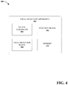
- FIG. 4 depicts a non-limiting schematic diagram of a fault detection apparatus according to various non-limiting aspects of the subject disclosure
- FIG. 5 depicts an exemplary flowchart of non-limiting methods associated with fault detection in a single circuit according to various non-limiting aspects of the disclosed subject matter.
- FIG. 6 depicts an example schematic block diagram for a computing environment in accordance with certain embodiments of this disclosure.
- MEMS sensor MEMS accelerometer, MEMS gyroscope, MEMS inertial sensor, MEMS acoustic sensor(s), MEMS audio sensor(s), and the like are used interchangeably unless context warrants a particular distinction among such terms.
- the terms can refer to MEMS devices or components that can measure acceleration, rate of rotation, a proximity, determine acoustic characteristics, generate acoustic signals, or the like.
- a test signal can be generated based on an input signal, and the input signal and test signal can be sent through the circuit and the resulting signals can be compared to determine if any fault is present.
- a function can be applied to bits of the input signal and bits of the test signal such that when the signals are compared after passing through the processing block that is to be tested, if the variation between the signals is above a predetermined amount, it can be determined that a fault has occurred.
- a first function can be applied to the input signal, and a second function can be applied to the test signal, and the resulting outputs can be compared.
- the input signal and test signal can be time multiplexed to generate a second output signal that can be used to determine the existence of a fault.
- the various embodiments can include other components and/or functionality. It is further noted that the various embodiments can be included in larger systems, including, smart televisions, smart phones or other cellular phones, wearables (e.g., watches, headphones, etc.), tablet computers, electronic reader devices (i.e., e-readers), laptop computers, desktop computers, monitors, digital recording devices, appliances, home electronics, handheld gaming devices, remote controllers (e.g., video game controllers, television controllers, etc.), automotive devices, personal electronic equipment, medical devices, industrial systems, cameras, and various other devices or fields.
- wearables e.g., watches, headphones, etc.
- electronic reader devices i.e., e-readers
- laptop computers desktop computers
- monitors digital recording devices
- appliances home electronics
- handheld gaming devices e.g., portable gaming devices
- remote controllers e.g., video game controllers, television controllers, etc.
- automotive devices personal electronic equipment, medical devices, industrial systems, cameras, and various other devices or fields.
- FIG. 1 illustrates an exemplary, non-limiting block diagram 100 of a fault detection system according to various non-limiting aspects of the subject disclosure.
- a signal 102 can be applied to a circuit to facilitate one or more functions and/or operations by a process block 112 .
- the process block 112 can include any processor, chip, or hardware logic that performs operations based on an input signal 102 .
- the operations can include executing instructions from a memory, or performing computations, or other operations.
- faults such as stuck-at-fault, bridging fault, transistor fault or open faults, short circuits, and other faults which may eventually cause functionality breakdown can be detected using a second signal, a test signal 104 .
- the test signal is applied using a separate circuit that overlaps with the tested circuit at the process block 112 that is to be tested.
- the test signal 104 can be applied to the same circuit, to avoid having to duplicate the circuit and waste silicon area and increased costs.
- the test signal 104 can be generated by a signal generator in some embodiments, or can be an altered and/or modified version of the signal 102 . This is represented in FIG. 1 as the signal 102 being “x” and the test signal 104 being “g(x)” where the test signal 104 is some function g of x.
- the test signal 104 and the signal 102 can each pass through a function block 106 that applies a first function to the primary signal 102 and a second function to the test signal 104 , resulting in a modified signal 108 that is a function of x, and a modified test signal 110 that is another function of g of x.
- the hashmark in the modified test signal 110 can indicate that the functions applied to the signals are different functions. In other embodiments however, the same functions can be applied to both the primary signal 102 and the test signal 104 .
- the second function applied to the test signal 104 can be an inverse function of the first function applied to the primary signal 102 .
- the test signal 104 is generated based on the primary signal 102 , wherein the digital bits corresponding to the test signal 104 are based on the digital bits representing the primary signal 102 .
- the function block 106 performs modifications to the digital bits representing the signal 102 and the test signal 104 .
- the signal generator or function block 106 can comprise digital logic or a digital adder that can invert the test signal 104 relative to the input signal 102 or can take a 2's complement or a 1's complement of bits of the primary signal 102 and test signal that results in the modified signals 108 and 110 .
- the test signal generator or function block can perform analog transformations of the signals (e.g., inverting, etc) that do not involve modifying digital bits of the signals.
- the modified input signal 108 and the modified test signal 110 can both be passed through the process block 112 and a fault detection system can determine whether a fault 114 has occurred based on the output of the process block 112 . It can be determined that the process block 112 has a fault 114 if the output signals 108 ′ and 110 ′ are outside a predetermined value.
- the function block 106 can apply the functions to signals 102 and 104 that result in modified signals 108 and 110 such that when the modified signals 108 and 110 pass through the process block 112 , the outputs ( 108 ′, 110 ′) cancel each other out or provide some specific result when added together or combined (e.g., a null value in an exemplary embodiment or another value in other embodiments).
- the fault detection system can determine that the process block 112 has a fault of some variety.
- the functions applied to the input signal 102 and the test signal 104 at 106 can be based on the type of process block 112 or the type of transformation performed in the process block 112 in order to facilitate comparing the test signal 110 ′ to the input signal 108 ′ to determine whether a fault exists.
- the fault detection can be altered based on the function applied and the process block 112 .
- the determination of whether a fault exists can be based on a range of resulting values. There can be some natural rounding up and down of values through the process block 112 , and the predetermined range around the target value can account for the rounding values.
- the test signal 104 can be introduced to the circuit after the input signal 102 is applied to the circuit.
- a test signal can be sequentially applied to the circuit after every input signal to provide continual testing, or test signals can be applied at various predetermined periods (e.g., every micro-second, millisecond, etc), using a previous input signal as a basis for the test signal.
- the circuit can contain one or more memories (e.g., FLASH, EEPROM, RAM, DRAM, SRAM, and etc) in order to retain a record of the input signal or the test signal until the corresponding signal is received in order to perform a comparison of the signals.
- test signal 104 can be applied to the circuit at substantially the same time as the input signal 102 , and the signals can be time domain multiplexed, frequency domain multiplexed, or form of multiplexing in order to transmit both the input signal 102 and the test signal 104 at substantially the same time.
- the input signal 102 can be one of many input signals, and there can be a one or more test signals corresponding to one or more of the input signals.
- the circuit can thus be tested for faults by making comparisons between the plurality of input signals and corresponding test signals.
- FIG. 2 illustrated is a non-limiting block diagram of a fault detection system according to various non-limiting aspects of the subject disclosure.
- the test signal 204 can be an inverse of the input signal 202 .
- the function block 206 can apply the same function to both the input signal 202 and the test signal 204 , resulting in a modified input signal 208 that is f(x) and a modified test signal 210 that is ⁇ f(x).
- the function block 206 can comprise digital logic that can invert the test signal 204 relative to the input signal 202 or can take a two's complement or one's complement of bits of the input signal 202 and test signal 204 that results in the modified signals 208 and 210 .
- the test signal generator or function block can perform analog transformations of the signals (e.g., inverting, etc) that do not involve modifying digital bits of signals.
- the modified signals 208 and 210 can be compared by digital logic 212 that adds digitalbits of the signal together. If there is no error, the result of the digital logic 212 should result in an output 214 of around 0.
- the fault detection system can also accept non-zero values as being fault free as long as the non-zero values are within a predetermined range of 0. This predetermined range accounts for levels of acceptable rounding and estimation that may be performed in the circuit. If the values of the output 214 are outside the predetermined range around zero however, the circuit may be determined to have a fault.
- the implementation can be suitable for an odd function, where the result of a function of x is negative for a negative x input, and the result of a function of x is positive for a positive x input.
- odd functions can be used with different implementations.
- the fault detection system 200 can be contained on a single circuit.
- the test signal 204 can be sequentially applied to the circuit after every input signal to provide continual testing, or test signals can be applied at various predetermined periods (e.g., every micro-second, milli-second, etc), using a previous input signal as a basis for the test signal.
- the circuit can contain one or more memories (e.g., FLASH, EEPROM, RAM, DRAM, SRAM, and etc) in order to retain a record of the input signal or the test signal until the corresponding signal is received in order to perform a comparison of the signals.
- the input signal 202 can be one of many input signals, and there can be a one or more test signals corresponding to one or more of the input signals.
- the circuit can thus be tested for faults by making comparisons between the plurality of input signals and corresponding test signals.
- FIG. 3 illustrated is a non-limiting block diagram 300 of a fault detection system that uses time multiplexing according to various non-limiting aspects of the subject disclosure.
- there can be multiple inputs at 302 e.g., X, Y, Z, as well as test signal ⁇ X, ⁇ Y, and ⁇ Z.
- These inputs and test signals can be multiplexed and one or more functions performed on them at 304 and 306 .
- the input signals can be compared to the test signals sequentially during extra phases, and their values determined at 310 . If the results are greater than a predetermined value, for example 2 least significant bits at 312 , it can be determined at 314 that there may be a fault in the circuit.
- a predetermined value for example 2 least significant bits at 312
- the fault detection system disclosed herein performs a function comprising a*x+b that includes fault detection.
- the fault detection apparatus 402 can include a signal generator 404 that generates a test signal 104204 , based on an input signal 102 , 202 and applies the test signal 104 , 204 to a circuit associated with the input signal 102 , 204 . See also, FIGS. 1 and 2 .
- a function block 406 can be included that applies a first function to the input signal 102 , 202 and a second function to the test signal 104 , 204 , resulting in a first signal 108 , 208 and a second signal 110 , 210 respectively wherein the second function is based on the first function.
- a fault detection block 408 can be included that receives the first signal 108 ′, 208 ′ and the second signal 110 ′, 210 ′ after the first signal and the second signal have passed through a process block that is to be tested and compares the first signal 108 ′, 208 ′ and second signal 110 ′, 210 ′ to determine whether the process block has a fault.
- a memory 410 can further be included to store information relating to the first signal until the second signal is received.
- the signal generator can generate the test signal based on an altered and/or modified version of the input signal.
- the test signal and the signal can each pass through the function block 406 that applies a first function to the primary signal and a second function to the test signal, resulting in a modified signal that is a function of x, and a modified test signal that is another function of x.
- the function block 406 can apply the same function to both the input signal and the test signal.
- the second function applied to the test signal can be an inverse function of the first function applied to the input signal.
- the test signal is generated based on the primary signal, wherein the bits of the test signal are based on bits of the primary signal.
- the function block 406 performs modifications to the bits of the signal and the test signal.
- the signal generator 404 or function block 406 can comprise digital logic or a digital adder that can invert the test signal relative to the input signal or can take a two's complement or one's complement of bits of the primary signal and test signal that results in the modified signals.
- the signal generator 404 or function block 406 can perform analog transformations of the signals (e.g., inverting, etc) that do not involve modifying bits of the signals.
- the signal generator 404 can introduce the test signal to the circuit after the input signal is applied to the circuit.
- a test signal can be applied to the circuit after every input signal to provide continual testing, or test signals can be applied at various predetermined periods (e.g., every micro-second, milli-second, etc), using a previous input signal as a basis for the test signal.
- the circuit can contain one or more memories (e.g., memory 410 ) in order to retain a record of the input signal or the test signal until the corresponding signal is received in order to perform a comparison of the signals.
- the fault detection block 408 can compare the outputs of the signals after passing through the chip or logic that is to be tested. By comparing the values of the signals the fault detection block 408 can determine that a fault has occurred if the sum of the values is outside a predetermined range around a predetermined value. If the test signal is inverse to the input signal, and the combination of the signals is not zero (or within a predetermined range of zero), then the fault detection block 408 can determine that the chip or logic contains a fault.
- FIG. 5 depicts an exemplary flowchart of non-limiting methods associated with fault detection in a single circuit according to various non-limiting aspects of the disclosed subject matter.
- exemplary method 500 can facilitate determining whether a circuit has a fault in a chip or digital logic based on a test signal that is applied to the same circuit as the input signal.
- the method 500 can start at 502 where the method includes applying a test signal to a circuit, wherein the test signal is derived from an input signal that has been applied to the circuit.
- the method includes applying the test signal and the input signal to a processing block.
- the method includes in response to receiving the test signal and input signal after passage through the process block, determining that the process block contains a fault in response to a sum of the bits of the test signal and input signal not equaling zero.
- a suitable environment 600 for implementing various aspects of the claimed subject matter includes a computer 602 .
- the computer 602 includes a processing unit 604 , a system memory 606 , sensor(s) 635 , and a system bus 608 .
- the system bus 608 couples system components including, but not limited to, the system memory 606 to the processing unit 604 .
- the processing unit 604 can be any of various available processors. Dual microprocessors and other multiprocessor architectures also can be employed as the processing unit 604 .
- the system bus 608 can be any of several types of bus structure(s) including the memory bus or memory controller, a peripheral bus or external bus, and/or a local bus using any variety of available bus architectures including, but not limited to, Industrial Standard Architecture (ISA), Micro-Channel Architecture (MSA), Extended ISA (EISA), Intelligent Drive Electronics (IDE), VESA Local Bus (VLB), Peripheral Component Interconnect (PCI), Card Bus, Universal Serial Bus (USB), Advanced Graphics Port (AGP), Personal Computer Memory Card International Association bus (PCMCIA), Firewire (IEEE 1394), and Small Computer Systems Interface (SCSI).
- ISA Industrial Standard Architecture
- MSA Micro-Channel Architecture
- EISA Extended ISA
- IDE Intelligent Drive Electronics
- VLB VESA Local Bus
- PCI Peripheral Component Interconnect
- Card Bus Universal Serial Bus
- USB Universal Serial Bus
- AGP Advanced Graphics Port
- PCMCIA Personal Computer Memory Card International Association bus
- Firewire IEEE 1394
- SCSI Small Computer Systems Interface
- the system memory 606 includes volatile memory 610 and non-volatile memory 612 .
- the basic input/output system (BIOS) containing the basic routines to transfer information between elements within the computer 602 , such as during start-up, is stored in non-volatile memory 612 .
- the processing unit 604 and or system memory can process and/or receive a digital signal received from the sensor 635 .
- the processing unit 604 can perform sampling on an analog signal received from the sensor 635 (e.g., sensor 308 ) using a clock signal received from the sensor 635 .
- non-volatile memory 612 can include read only memory (ROM), programmable ROM (PROM), electrically programmable ROM (EPROM), electrically erasable programmable ROM (EEPROM), or flash memory.
- Volatile memory 610 includes random access memory (RAM), which acts as external cache memory. According to present aspects, the volatile memory may store the write operation retry logic (not shown in FIG. 6 ) and the like.
- RAM is available in many forms such as static RAM (SRAM), dynamic RAM (DRAM), synchronous DRAM (SDRAM), double data rate SDRAM (DDR SDRAM), and enhanced SDRAM (ESDRAM).
- Disk storage 614 includes, but is not limited to, devices like a magnetic disk drive, solid state disk (SSD) floppy disk drive, tape drive, Jaz drive, Zip drive, LS-100 drive, flash memory card, or memory stick.
- disk storage 614 can include storage medium separately or in combination with other storage medium including, but not limited to, an optical disk drive such as a compact disk ROM device (CD-ROM), CD recordable drive (CD-R Drive), CD rewritable drive (CD-RW Drive) or a digital versatile disk ROM drive (DVD-ROM).
- CD-ROM compact disk ROM device
- CD-R Drive CD recordable drive
- CD-RW Drive CD rewritable drive
- DVD-ROM digital versatile disk ROM drive
- storage devices 614 can store information related to a user. Such information might be stored at or provided to a server or to an application running on a user device. In one embodiment, the user can be notified (e.g., by way of output device(s) 636 ) of the types of information that are stored to disk storage 614 and/or transmitted to the server or application. The user can be provided the opportunity to control having such information collected and/or shared with the server or application (e.g., by way of input from input device(s) 628 ).
- FIG. 6 describes software that acts as an intermediary between users and the basic computer resources described in the suitable operating environment 600 .
- Such software includes an operating system 618 .
- Operating system 618 which can be stored on disk storage 614 , acts to control and allocate resources of the computer system 602 .
- Applications 620 take advantage of the management of resources by operating system 618 through program modules 624 , and program data 626 , such as the boot/shutdown transaction table and the like, stored either in system memory 606 or on disk storage 614 . It is to be appreciated that the claimed subject matter can be implemented with various operating systems or combinations of operating systems.
- a user enters commands or information into the computer 602 through input device(s) 628 .
- Input devices 628 include, but are not limited to, a pointing device such as a mouse, trackball, stylus, touch pad, keyboard, microphone, joystick, game pad, satellite dish, scanner, TV tuner card, digital camera, digital video camera, web camera, and the like.
- These and other input devices connect to the processing unit 604 through the system bus 608 via interface port(s) 630 .
- Interface port(s) 630 include, for example, a serial port, a parallel port, a game port, and a universal serial bus (USB).
- Output device(s) 636 use some of the same type of ports as input device(s) 628 .
- a USB port may be used to provide input to computer 602 and to output information from computer 602 to an output device 636 .
- Output adapter 634 is provided to illustrate that there are some output devices 636 like monitors, speakers, and printers, among other output devices 636 , which require special adapters.
- the output adapters 634 include, by way of illustration and not limitation, video and sound cards that provide a means of connection between the output device 636 and the system bus 608 . It should be noted that other devices and/or systems of devices provide both input and output capabilities such as remote computer(s) 638 .
- Computer 602 can operate in a networked environment using logical connections to one or more remote computers, such as remote computer(s) 638 .
- the remote computer(s) 638 can be a personal computer, a server, a router, a network PC, a workstation, a microprocessor based appliance, a peer device, a smart phone, a tablet, or other network node, and typically includes many of the elements described relative to computer 602 .
- only a memory storage device 640 is illustrated with remote computer(s) 638 .
- Remote computer(s) 638 is logically connected to computer 602 through a network interface 642 and then connected via communication connection(s) 644 .
- Network interface 642 encompasses wire and/or wireless communication networks such as local-area networks (LAN) and wide-area networks (WAN) and cellular networks.
- LAN technologies include Fiber Distributed Data Interface (FDDI), Copper Distributed Data Interface (CDDI), Ethernet, Token Ring and the like.
- WAN technologies include, but are not limited to, point-to-point links, circuit switching networks like Integrated Services Digital Networks (ISDN) and variations thereon, packet switching networks, and Digital Subscriber Lines (DSL).
- ISDN Integrated Services Digital Networks
- DSL Digital Subscriber Lines
- Communication connection(s) 644 refers to the hardware/software employed to connect the network interface 642 to the bus 608 . While communication connection 644 is shown for illustrative clarity inside computer 602 , it can also be external to computer 602 .
- the hardware/software necessary for connection to the network interface 642 includes, for exemplary purposes only, internal and external technologies such as, modems including regular telephone grade modems, cable modems and DSL modems, ISDN adapters, and wired and wireless Ethernet cards, hubs, and routers.
- Computer 602 can also include a fault detection engine 646 and controller 648 that perform the functions associated with the fault detection apparatus 402 described above with reference to FIG. 4 .
- the illustrated aspects of the disclosure may also be practiced in distributed computing environments where certain tasks are performed by remote processing devices that are linked through a communications network.
- program modules can be located in both local and remote memory storage devices.
- various components described herein can include electrical circuit(s) that can include components and circuitry elements of suitable value in order to implement the embodiments of the subject innovation(s).
- many of the various components can be implemented on one or more integrated circuit (IC) chips.
- IC integrated circuit
- a set of components can be implemented in a single IC chip.
- one or more of respective components are fabricated or implemented on separate IC chips.
- the terms used to describe such components are intended to correspond, unless otherwise indicated, to any component which performs the specified function of the described component (e.g., a functional equivalent), even though not structurally equivalent to the disclosed structure, which performs the function in the herein illustrated exemplary aspects of the claimed subject matter.
- the innovation includes a system as well as a computer-readable storage medium having computer-executable instructions for performing the acts and/or events of the various methods of the claimed subject matter.
- one or more components may be combined into a single component providing aggregate functionality or divided into several separate sub-components, and any one or more middle layers, such as a management layer, may be provided to communicatively couple to such sub-components in order to provide integrated functionality.
- middle layers such as a management layer
- Any components described herein may also interact with one or more other components not specifically described herein but known by those of skill in the art.
- a component may be, but is not limited to being, a process running on a processor (e.g., digital signal processor), a processor, an object, an executable, a thread of execution, a program, and/or a computer.
- a processor e.g., digital signal processor
- an application running on a controller and the controller can be a component.
- One or more components may reside within a process and/or thread of execution and a component may be localized on one computer and/or distributed between two or more computers.
- a “device” can come in the form of specially designed hardware; generalized hardware made specialized by the execution of software thereon that enables the hardware to perform specific function; software stored on a computer readable medium; or a combination thereof.
- example or “exemplary” are used herein to mean serving as an example, instance, or illustration. Any aspect or design described herein as “exemplary” is not necessarily to be construed as preferred or advantageous over other aspects or designs. Rather, use of the words “example” or “exemplary” is intended to present concepts in a concrete fashion.
- the term “or” is intended to mean an inclusive “or” rather than an exclusive “or”. That is, unless specified otherwise, or clear from context, “X employs A or B” is intended to mean any of the natural inclusive permutations.
Abstract
Description
Claims (22)
Priority Applications (3)
| Application Number | Priority Date | Filing Date | Title |
|---|---|---|---|
| US15/471,539 US10830816B2 (en) | 2017-03-28 | 2017-03-28 | Single circuit fault detection |
| JP2019552453A JP7125417B2 (en) | 2017-03-28 | 2018-03-27 | Single circuit fault detection |
| PCT/US2018/024563 WO2018183324A1 (en) | 2017-03-28 | 2018-03-27 | Single circuit fault detection |
Applications Claiming Priority (1)
| Application Number | Priority Date | Filing Date | Title |
|---|---|---|---|
| US15/471,539 US10830816B2 (en) | 2017-03-28 | 2017-03-28 | Single circuit fault detection |
Publications (2)
| Publication Number | Publication Date |
|---|---|
| US20180284188A1 US20180284188A1 (en) | 2018-10-04 |
| US10830816B2 true US10830816B2 (en) | 2020-11-10 |
Family
ID=61972617
Family Applications (1)
| Application Number | Title | Priority Date | Filing Date |
|---|---|---|---|
| US15/471,539 Active US10830816B2 (en) | 2017-03-28 | 2017-03-28 | Single circuit fault detection |
Country Status (3)
| Country | Link |
|---|---|
| US (1) | US10830816B2 (en) |
| JP (1) | JP7125417B2 (en) |
| WO (1) | WO2018183324A1 (en) |
Families Citing this family (2)
| Publication number | Priority date | Publication date | Assignee | Title |
|---|---|---|---|---|
| US10837999B2 (en) * | 2018-09-21 | 2020-11-17 | Invensense, Inc. | Fault detection of a system using a test input comprising a linear combination of inputs of the system |
| CN111443280B (en) * | 2020-05-11 | 2021-05-11 | 李江 | Equipment for detecting precision and electrical performance of mouse PCB |
Citations (3)
| Publication number | Priority date | Publication date | Assignee | Title |
|---|---|---|---|---|
| US6092217A (en) * | 1993-10-15 | 2000-07-18 | Hitachi, Ltd. | Logic circuit having error detection function, redundant resource management method and fault tolerant system using it |
| US6253350B1 (en) * | 1998-07-09 | 2001-06-26 | International Business Machines Corporation | Method and system for detecting errors within complementary logic circuits |
| US20140019818A1 (en) * | 2012-07-12 | 2014-01-16 | Freescale Semiconductor | System for testing error detection circuits |
Family Cites Families (5)
| Publication number | Priority date | Publication date | Assignee | Title |
|---|---|---|---|---|
| US7239978B2 (en) | 2004-03-31 | 2007-07-03 | Wu-Tung Cheng | Compactor independent fault diagnosis |
| DE102009011431A1 (en) | 2009-02-25 | 2010-08-26 | Iav Gmbh Ingenieurgesellschaft Auto Und Verkehr | Drive system controlling and regulating device for motor vehicle, has computer program code structured in blocks, and actuator-interface comprising two levels that are separated from each other by runtime environment |
| JP5649810B2 (en) | 2009-10-29 | 2015-01-07 | 日立オートモティブシステムズ株式会社 | Capacitive sensor |
| US9634567B2 (en) * | 2015-02-17 | 2017-04-25 | Invensense, Inc. | Sensor data acquisition system with integrated power management |
| US20170055093A1 (en) * | 2015-08-19 | 2017-02-23 | Invensense, Inc. | Dynamically programmable microphone |
-
2017
- 2017-03-28 US US15/471,539 patent/US10830816B2/en active Active
-
2018
- 2018-03-27 JP JP2019552453A patent/JP7125417B2/en active Active
- 2018-03-27 WO PCT/US2018/024563 patent/WO2018183324A1/en active Application Filing
Patent Citations (3)
| Publication number | Priority date | Publication date | Assignee | Title |
|---|---|---|---|---|
| US6092217A (en) * | 1993-10-15 | 2000-07-18 | Hitachi, Ltd. | Logic circuit having error detection function, redundant resource management method and fault tolerant system using it |
| US6253350B1 (en) * | 1998-07-09 | 2001-06-26 | International Business Machines Corporation | Method and system for detecting errors within complementary logic circuits |
| US20140019818A1 (en) * | 2012-07-12 | 2014-01-16 | Freescale Semiconductor | System for testing error detection circuits |
Non-Patent Citations (1)
| Title |
|---|
| English translation of International Search Report and Written Opinion issued in International Patent Application No. PCT/US2018/024563, dated Jul. 9, 2018. |
Also Published As
| Publication number | Publication date |
|---|---|
| US20180284188A1 (en) | 2018-10-04 |
| JP2020515833A (en) | 2020-05-28 |
| WO2018183324A1 (en) | 2018-10-04 |
| JP7125417B2 (en) | 2022-08-24 |
Similar Documents
| Publication | Publication Date | Title |
|---|---|---|
| CN109347787B (en) | Identity information identification method and device | |
| US10614905B2 (en) | System for testing memory and method thereof | |
| WO2020078059A1 (en) | Interpretation feature determination method and device for anomaly detection | |
| US9276583B1 (en) | Soft dark bit masking with integrated load modulation and burn-in induced destabilization for physically unclonable function keys | |
| US10830816B2 (en) | Single circuit fault detection | |
| CN109213703B (en) | Data detection method and data detection device | |
| US20180239905A1 (en) | Method, checking device, and system for determining security of a processor | |
| WO2019001334A1 (en) | Stack overflow processing method and device | |
| US9514028B2 (en) | System and method for determining correct execution of software based on baseline and real time trace events | |
| CN112434478B (en) | Method for simulating virtual interface of logic system design and related equipment | |
| Hinrichs et al. | Model Check What You Can, Runtime Verify the Rest. | |
| JP2000132430A (en) | Signal processor | |
| US7617428B2 (en) | Circuits and associated methods for improved debug and test of an application integrated circuit | |
| CN108647422B (en) | Port delay constraint method and device | |
| KR101334111B1 (en) | Quad-data rate controller and realization method thereof | |
| US20090160488A1 (en) | Apparatus and method for clock signal synchronization in JTAG testing in systems having modules processing clock signals at different rates | |
| CN107122665B (en) | Leak detection method and Hole Detection device | |
| US10872030B2 (en) | Control system and method of to perform an operation | |
| CN117236277B (en) | Method and device for checking register and electronic equipment | |
| US11061745B2 (en) | Shared resource analysis for embedded multi-core systems | |
| CN105374396A (en) | Semiconductor apparatus | |
| CN106411900B (en) | Method and device based on virtualized hardware scanning | |
| Kim et al. | Acquisition accuracy enhancement of high-speed storage interface signals | |
| CN117971753A (en) | Communication method and device | |
| KR20060126149A (en) | Apparatus for sensing bus traffic and method for sensing a amount of bus traffic |
Legal Events
| Date | Code | Title | Description |
|---|---|---|---|
| AS | Assignment |
Owner name: INVENSENSE, INC., CALIFORNIA Free format text: ASSIGNMENT OF ASSIGNORS INTEREST;ASSIGNORS:OLIAEI, OMID;GIAMBASTIANI, ADOLFO;SIGNING DATES FROM 20170323 TO 20170324;REEL/FRAME:041769/0826 |
|
| AS | Assignment |
Owner name: PANASONIC CORPORATION, JAPAN Free format text: ASSIGNMENT OF ASSIGNORS INTEREST;ASSIGNORS:INVENSENSE, INC.;INVENSENSE INTERNATIONAL, INC.;REEL/FRAME:046841/0560 Effective date: 20180602 |
|
| STPP | Information on status: patent application and granting procedure in general |
Free format text: FINAL REJECTION MAILED |
|
| STPP | Information on status: patent application and granting procedure in general |
Free format text: DOCKETED NEW CASE - READY FOR EXAMINATION |
|
| STPP | Information on status: patent application and granting procedure in general |
Free format text: NOTICE OF ALLOWANCE MAILED -- APPLICATION RECEIVED IN OFFICE OF PUBLICATIONS |
|
| STPP | Information on status: patent application and granting procedure in general |
Free format text: DOCKETED NEW CASE - READY FOR EXAMINATION |
|
| STPP | Information on status: patent application and granting procedure in general |
Free format text: NON FINAL ACTION MAILED |
|
| STPP | Information on status: patent application and granting procedure in general |
Free format text: FINAL REJECTION MAILED |
|
| STPP | Information on status: patent application and granting procedure in general |
Free format text: ADVISORY ACTION MAILED |
|
| STPP | Information on status: patent application and granting procedure in general |
Free format text: PUBLICATIONS -- ISSUE FEE PAYMENT VERIFIED |
|
| STCF | Information on status: patent grant |
Free format text: PATENTED CASE |