JP5618963B2 - Semiconductor device - Google Patents
Semiconductor device Download PDFInfo
- Publication number
- JP5618963B2 JP5618963B2 JP2011234814A JP2011234814A JP5618963B2 JP 5618963 B2 JP5618963 B2 JP 5618963B2 JP 2011234814 A JP2011234814 A JP 2011234814A JP 2011234814 A JP2011234814 A JP 2011234814A JP 5618963 B2 JP5618963 B2 JP 5618963B2
- Authority
- JP
- Japan
- Prior art keywords
- semiconductor layer
- semiconductor
- semiconductor substrate
- semiconductor device
- transistor
- Prior art date
- Legal status (The legal status is an assumption and is not a legal conclusion. Google has not performed a legal analysis and makes no representation as to the accuracy of the status listed.)
- Active
Links
Images


Classifications
-
- H—ELECTRICITY
- H01—ELECTRIC ELEMENTS
- H01L—SEMICONDUCTOR DEVICES NOT COVERED BY CLASS H10
- H01L27/00—Devices consisting of a plurality of semiconductor or other solid-state components formed in or on a common substrate
- H01L27/02—Devices consisting of a plurality of semiconductor or other solid-state components formed in or on a common substrate including semiconductor components specially adapted for rectifying, oscillating, amplifying or switching and having at least one potential-jump barrier or surface barrier; including integrated passive circuit elements with at least one potential-jump barrier or surface barrier
- H01L27/04—Devices consisting of a plurality of semiconductor or other solid-state components formed in or on a common substrate including semiconductor components specially adapted for rectifying, oscillating, amplifying or switching and having at least one potential-jump barrier or surface barrier; including integrated passive circuit elements with at least one potential-jump barrier or surface barrier the substrate being a semiconductor body
- H01L27/06—Devices consisting of a plurality of semiconductor or other solid-state components formed in or on a common substrate including semiconductor components specially adapted for rectifying, oscillating, amplifying or switching and having at least one potential-jump barrier or surface barrier; including integrated passive circuit elements with at least one potential-jump barrier or surface barrier the substrate being a semiconductor body including a plurality of individual components in a non-repetitive configuration
- H01L27/0611—Devices consisting of a plurality of semiconductor or other solid-state components formed in or on a common substrate including semiconductor components specially adapted for rectifying, oscillating, amplifying or switching and having at least one potential-jump barrier or surface barrier; including integrated passive circuit elements with at least one potential-jump barrier or surface barrier the substrate being a semiconductor body including a plurality of individual components in a non-repetitive configuration integrated circuits having a two-dimensional layout of components without a common active region
- H01L27/0617—Devices consisting of a plurality of semiconductor or other solid-state components formed in or on a common substrate including semiconductor components specially adapted for rectifying, oscillating, amplifying or switching and having at least one potential-jump barrier or surface barrier; including integrated passive circuit elements with at least one potential-jump barrier or surface barrier the substrate being a semiconductor body including a plurality of individual components in a non-repetitive configuration integrated circuits having a two-dimensional layout of components without a common active region comprising components of the field-effect type
- H01L27/0629—Devices consisting of a plurality of semiconductor or other solid-state components formed in or on a common substrate including semiconductor components specially adapted for rectifying, oscillating, amplifying or switching and having at least one potential-jump barrier or surface barrier; including integrated passive circuit elements with at least one potential-jump barrier or surface barrier the substrate being a semiconductor body including a plurality of individual components in a non-repetitive configuration integrated circuits having a two-dimensional layout of components without a common active region comprising components of the field-effect type in combination with diodes, or resistors, or capacitors
-
- H—ELECTRICITY
- H01—ELECTRIC ELEMENTS
- H01L—SEMICONDUCTOR DEVICES NOT COVERED BY CLASS H10
- H01L27/00—Devices consisting of a plurality of semiconductor or other solid-state components formed in or on a common substrate
- H01L27/02—Devices consisting of a plurality of semiconductor or other solid-state components formed in or on a common substrate including semiconductor components specially adapted for rectifying, oscillating, amplifying or switching and having at least one potential-jump barrier or surface barrier; including integrated passive circuit elements with at least one potential-jump barrier or surface barrier
- H01L27/04—Devices consisting of a plurality of semiconductor or other solid-state components formed in or on a common substrate including semiconductor components specially adapted for rectifying, oscillating, amplifying or switching and having at least one potential-jump barrier or surface barrier; including integrated passive circuit elements with at least one potential-jump barrier or surface barrier the substrate being a semiconductor body
- H01L27/06—Devices consisting of a plurality of semiconductor or other solid-state components formed in or on a common substrate including semiconductor components specially adapted for rectifying, oscillating, amplifying or switching and having at least one potential-jump barrier or surface barrier; including integrated passive circuit elements with at least one potential-jump barrier or surface barrier the substrate being a semiconductor body including a plurality of individual components in a non-repetitive configuration
- H01L27/07—Devices consisting of a plurality of semiconductor or other solid-state components formed in or on a common substrate including semiconductor components specially adapted for rectifying, oscillating, amplifying or switching and having at least one potential-jump barrier or surface barrier; including integrated passive circuit elements with at least one potential-jump barrier or surface barrier the substrate being a semiconductor body including a plurality of individual components in a non-repetitive configuration the components having an active region in common
- H01L27/0705—Devices consisting of a plurality of semiconductor or other solid-state components formed in or on a common substrate including semiconductor components specially adapted for rectifying, oscillating, amplifying or switching and having at least one potential-jump barrier or surface barrier; including integrated passive circuit elements with at least one potential-jump barrier or surface barrier the substrate being a semiconductor body including a plurality of individual components in a non-repetitive configuration the components having an active region in common comprising components of the field effect type
- H01L27/0711—Devices consisting of a plurality of semiconductor or other solid-state components formed in or on a common substrate including semiconductor components specially adapted for rectifying, oscillating, amplifying or switching and having at least one potential-jump barrier or surface barrier; including integrated passive circuit elements with at least one potential-jump barrier or surface barrier the substrate being a semiconductor body including a plurality of individual components in a non-repetitive configuration the components having an active region in common comprising components of the field effect type in combination with bipolar transistors and diodes, or capacitors, or resistors
- H01L27/0716—Devices consisting of a plurality of semiconductor or other solid-state components formed in or on a common substrate including semiconductor components specially adapted for rectifying, oscillating, amplifying or switching and having at least one potential-jump barrier or surface barrier; including integrated passive circuit elements with at least one potential-jump barrier or surface barrier the substrate being a semiconductor body including a plurality of individual components in a non-repetitive configuration the components having an active region in common comprising components of the field effect type in combination with bipolar transistors and diodes, or capacitors, or resistors in combination with vertical bipolar transistors and diodes, or capacitors, or resistors
Description
本発明は、電力用の半導体装置に関し、特に同一の半導体基板内に電力素子と回路素子とを形成する半導体装置に関する。 The present invention relates to a power semiconductor device, and more particularly to a semiconductor device in which a power element and a circuit element are formed in the same semiconductor substrate.
近年、電力用の半導体装置では、接続する負荷に電力を供給する電力素子と、電力素子を制御する回路素子とを同一の半導体基板に形成する構造が開発されている。電力素子と、回路素子とを同一の半導体基板に形成した半導体装置では、通常の動作において、回路素子を構成するp型の深い半導体層(GND接地)の電位に対して、半導体基板の電位が低くなることはない。そのため、回路素子を構成するNMOS(N-channel Metal-Oxide-Semiconductor)と半導体基板との間に形成される寄生素子(寄生NPNトランジスタ)は、通常動作において作動することがなく、半導体装置が誤動作することはない。 In recent years, a power semiconductor device has been developed in which a power element that supplies power to a connected load and a circuit element that controls the power element are formed on the same semiconductor substrate. In a semiconductor device in which a power element and a circuit element are formed on the same semiconductor substrate, the potential of the semiconductor substrate is lower than the potential of the p-type deep semiconductor layer (GND ground) constituting the circuit element in normal operation. It will never go down. Therefore, the parasitic element (parasitic NPN transistor) formed between the NMOS (N-channel Metal-Oxide-Semiconductor) constituting the circuit element and the semiconductor substrate does not operate in normal operation, and the semiconductor device malfunctions. Never do.
しかし、半導体装置に負電流が流れた場合、回路素子を構成するp型の深い半導体層の電位に対して、半導体基板の電位が低くなり、p型の半導体層から半導体基板に寄生電流が流れて寄生素子が作動する。半導体装置は、寄生素子が作動すると、誤動作する可能性がある。 However, when a negative current flows through the semiconductor device, the potential of the semiconductor substrate is lower than the potential of the p-type deep semiconductor layer constituting the circuit element, and a parasitic current flows from the p-type semiconductor layer to the semiconductor substrate. The parasitic element is activated. A semiconductor device may malfunction when a parasitic element is activated.
特許文献1および特許文献2には、半導体装置に形成される寄生素子を作動させず、半導体装置の誤動作を防止する構成が開示してある。
特許文献1に開示されている半導体装置では、寄生素子を作動させないために、電力素子のトランジスタと回路素子との間に第1のダミー領域を形成し、トランジスタと半導体基板の端との間に第2のダミー領域とを形成してある。そして、第1及び第2のダミー領域は、半導体基板とは異なった導電型であり、第2のダミー領域はトランジスタと第1のダミー領域との間にある半導体基板部分とに接続されている。
In the semiconductor device disclosed in
また、特許文献2に開示してある半導体装置では、寄生素子を作動させないために、素子分離領域と内部回路のGNDラインが、GNDパッドから配線層により直接接続せず、抵抗素子を介して接続してある。
Further, in the semiconductor device disclosed in
電力素子と、回路素子とを同一の半導体基板に形成した半導体装置では、回路素子を構成するNMOSと半導体基板との間に寄生素子が形成される。この半導体装置において、負電流が流れた場合、回路素子を構成するp型の深い半導体層の電位に対して、半導体基板の電位が低くなり寄生素子が作動して、半導体装置の誤動作が発生する。 In a semiconductor device in which a power element and a circuit element are formed on the same semiconductor substrate, a parasitic element is formed between the NMOS constituting the circuit element and the semiconductor substrate. In this semiconductor device, when a negative current flows, the potential of the semiconductor substrate becomes lower than the potential of the p-type deep semiconductor layer constituting the circuit element, and the parasitic element operates to cause a malfunction of the semiconductor device. .
それゆえに、本発明は、上記問題点を解決するためになされたものであり、半導体装置に負電流が流れた場合でも、回路素子を構成する深い半導体層の電位に対して、半導体基板の電位が低くなるのを抑制して寄生素子を作動させず、半導体装置の誤動作を防止する。 Therefore, the present invention has been made to solve the above-described problems. Even when a negative current flows through the semiconductor device, the potential of the semiconductor substrate with respect to the potential of the deep semiconductor layer constituting the circuit element. Is suppressed, the parasitic element is not operated, and the malfunction of the semiconductor device is prevented.
上記課題を解決するために、本発明は、第1導電型の半導体基板と、半導体基板の一面に形成し、接続する負荷に電力を供給する電力素子と、電力素子を形成した半導体基板の一面に形成し、第1導電型のソース・ドレイン領域を有するMOSトランジスタを少なくとも1つ含む回路素子と、電力素子を形成した半導体基板の一面に形成し、電力素子および回路素子に対し独立して配置した第2導電型の第1半導体層と、半導体基板および第1半導体層と接続する外部回路とを備えている。外部回路は、第1電源と、第1電源に一端を接続する第1抵抗素子と、第1抵抗素子の他端にアノード電極を接続し、カソード電極をGND接地する第1ダイオードとを有し、第1抵抗素子の他端に第1半導体層を接続する。 In order to solve the above-described problems, the present invention provides a first conductivity type semiconductor substrate, a power element formed on one surface of the semiconductor substrate and supplying power to a connected load, and one surface of the semiconductor substrate on which the power element is formed. A circuit element including at least one MOS transistor having a source / drain region of the first conductivity type, and formed on one surface of a semiconductor substrate on which the power element is formed, and disposed independently with respect to the power element and the circuit element And a first semiconductor layer of the second conductivity type and an external circuit connected to the semiconductor substrate and the first semiconductor layer. The external circuit includes a first power source, a first resistance element having one end connected to the first power source, and a first diode having an anode electrode connected to the other end of the first resistance element and a cathode electrode grounded to GND. The first semiconductor layer is connected to the other end of the first resistance element.
本発明に係る半導体装置によれば、半導体装置に負電流が流れた場合でも、回路素子を構成する深い半導体層の電位に対して、半導体基板の電位が低くなるのを抑制して寄生素子を作動させず、半導体装置の誤動作を防止する。 According to the semiconductor device of the present invention, even when a negative current flows in the semiconductor device, the potential of the semiconductor substrate is suppressed from being lowered with respect to the potential of the deep semiconductor layer constituting the circuit element, and the parasitic element is reduced. The semiconductor device is prevented from malfunctioning without being operated.
以下、本発明に係る実施の形態について図面を参照して説明する。
(実施の形態1)
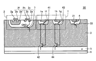
図1は、本発明の実施の形態1に係る半導体装置の構成を示す概略図である。図1に示す半導体装置10は、電力用であり、接続する負荷に電力を供給する電力素子1と、電力素子1を制御する回路素子2とを同一の半導体基板3に形成してある。さらに、半導体基板3には、電力素子1を形成した一面に、電力素子1および回路素子2に対し独立して配置したp型の半導体層4が形成してある。
Hereinafter, embodiments according to the present invention will be described with reference to the drawings.
(Embodiment 1)
FIG. 1 is a schematic diagram showing a configuration of a semiconductor device according to the first embodiment of the present invention. A
半導体基板3は、n型のシリコン基板であり、一面に電力素子1および回路素子2を形成してある。また、半導体基板3は、電力素子1および回路素子2を形成した一面の反対側の面に、p型の半導体層5、裏面電極6を積層してある。
The
電力素子1には、p型の半導体層1a内に、n型のソース・ドレイン領域1bを有するMOSトランジスタ1cが形成してある。
In the
回路素子2には、p型の半導体層2a内に、n型のソース・ドレイン領域2bを有するMOSトランジスタ2cが形成してある。ここで、p型の半導体層2aは、p型の半導体層1aに比べて深く形成してある。さらに、半導体基板3には、p型の半導体層2a内にn型の半導体層2dを形成し、形成した半導体層2d内にp型のソース・ドレイン領域2eを有するMOSトランジスタ2fが形成してある。なお、p型のソース・ドレイン領域2eの間には、ゲート電極2gが形成してある。同様に、n型のソース・ドレイン領域1bの間、およびn型のソース・ドレイン領域2bの間にもゲート電極1d,2hが形成してある。
In the
図1に示した電力素子1および回路素子2の構成は例示であり、MOSトランジスタ1c,2c,2fに限定されるものではなく、他の構成の素子を形成してもよい。ただし、回路素子2には、MOSトランジスタ2cを少なくとも1つ含むものとする。そのため、回路素子2には、MOSトランジスタ2cと半導体基板3との間に寄生素子が形成され、具体的に、n型のソース・ドレイン領域2bと、p型の半導体層2aと、n型の半導体基板3とで構成される寄生NPNトランジスタ7が半導体基板3に形成される。
The configurations of the
p型の半導体層4は、n型の半導体基板3に形成してあるので、pn接合のダイオード8を構成する。
Since the p-
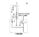
図1には図示していないが、半導体装置10には、半導体基板3および半導体層4と接続する外部回路を備えている。外部回路を含めた半導体装置10の等価回路を説明する。図2は、本発明の実施の形態1に係る半導体装置10の回路構成を示す回路図である。
Although not shown in FIG. 1, the
図2に示す外部回路9は、電源9aと、電源9aに一端を接続する抵抗素子9bと、抵抗素子9bの他端にアノード電極を接続し、カソード電極をGND接地するダイオード9cとを有している。また、抵抗素子9bの他端は、ダイオード8のアノード電極(半導体層4)と電気的に接続してある。
The
図2に示す半導体装置10では、電源9aに抵抗素子9bおよびダイオード9cを直列に接続することによって、ダイオード9cのアノード電極での電位が、たとえばダイオード9cの順方向降下電圧VFに対応する0.7V程度(常温)となる。これにより、半導体層4の電位を0.7V程度に固定し、半導体基板3の電位を、半導体層4の電位から0.7V程度低下した0V程度にする。
In the
半導体装置10は、電力素子1が通常動作によるオン状態の間、半導体基板3の電位が電力素子1のコレクタ−エミッタ間飽和電圧VCE(saturation)となる。また、半導体装置10は、電力素子1が通常動作によるオフ状態の間、裏面電極6の電位が半導体基板3の電位に比べて高電位となるため、半導体基板3の電位が負電位となることはない。
In the
しかし、半導体装置10に負電流が流れた場合、半導体基板3の電位が負電位となる。負電流が流れ半導体基板3の電位が負電位となった場合、外部回路9を備えていない従来の半導体装置では、半導体層2aの電位に対して半導体基板3の電位が低くなるので寄生NPNトランジスタ7がオン状態となり、半導体層2aから半導体基板3へ寄生電流が流れて、寄生NPNトランジスタ7が作動する。
However, when a negative current flows through the
半導体装置10では、負電流が流れた場合でも、ダイオード9cによって半導体層4の電位を0.7V程度に固定することができるため、半導体基板3の電位が負電位となることなく、0V程度に維持することができる。これにより、半導体装置10では、半導体層2aの電位と半導体基板3の電位とをほぼ同電位にすることができ、寄生NPNトランジスタ7がオン状態とならず、半導体層2aから半導体基板3へ寄生電流が流れないため、寄生NPNトランジスタ7が作動しない。
In the
以上のように、本発明の実施の形態1に係る半導体装置10では、ダイオード9cによって半導体層4の電位を0.7V程度に固定することができるため、負電流が流れた場合でも、回路素子を構成するp型の半導体層2aの電位に対して、半導体基板3の電位が低くなるのを抑制して寄生NPNトランジスタ7を作動させず、半導体装置10の誤動作を防止する。なお、半導体装置10は、誤動作を防止することで、誤動作による特性の劣化を抑えることができ、より長期間使用することが可能となる。
As described above, in the
(実施の形態2)
実施の形態1に係る半導体装置10では、負電流が流れた場合、半導体層4に構成されるダイオード8の順方向に電流が導通し、ダイオード8を流れる電流が増加する。ダイオード8を流れる電流が増加すると、抵抗素子9bによる電圧降下によってダイオード9cのアノード電極の電位(半導体層4の電位)が下がる。
(Embodiment 2)
In the
抵抗素子9bによる電圧降下によってダイオード9cのアノード電極の電位が、ダイオード9cの順方向降下電圧VF(たとえば、0.7V)以下になると、ダイオード9cがオフ状態となり電流が導通しなくなる。ダイオード9cの順方向に電流が導通しなくなると、半導体層4の電位を固定することができなくなる。
When the potential of the anode electrode of the
さらに、抵抗素子9bによる電圧降下が大きくなることによってダイオード9cのアノード電極の電位が0V以下になると、半導体基板3の電位が、半導体層2aの電位に対して0.7V以上低下することになるため、寄生NPNトランジスタ7が作動する。つまりは、抵抗素子9bによる電圧降下が大きくなることで、半導体装置10が誤動作する恐れがある。
Further, when the voltage drop due to the
そこで、本発明の実施の形態2に係る半導体装置では、半導体層4に構成されるダイオード8に代えて、半導体層4にトランジスタを構成する。図3は、本発明の実施の形態2に係る半導体装置の構成を示す概略図である。図3に示す半導体装置20は、電力用であり、接続する負荷に電力を供給する電力素子1と、電力素子1を制御する回路素子2とを同一の半導体基板3に形成してある。さらに、半導体基板3には、電力素子1を形成した一面に、電力素子1および回路素子2に対し独立して配置したp型の半導体層4が形成してある。また、半導体装置20は、半導体層4内に、n型の半導体層21を形成してある。
Therefore, in the semiconductor device according to the second embodiment of the present invention, a transistor is formed in the
なお、本発明の実施の形態2に係る半導体装置20は、実施の形態1に係る半導体装置10と同じ構成要素について同じ符号を付して、詳細な説明を省略する。
Note that, in the
p型の半導体層4内にn型の半導体層21を形成してあるので、n型の半導体層21と、p型の半導体層4と、n型の半導体基板3とで構成されるNPNトランジスタ22が半導体基板3に形成される。
Since the n-
図3には図示していないが、半導体装置20には、半導体基板3および半導体層4と接続する外部回路を備えている。外部回路を含めた半導体装置20の等価回路を説明する。図4は、本発明の実施の形態2に係る半導体装置20の回路構成を示す回路図である。
Although not shown in FIG. 3, the
図4に示す外部回路9は、電源9aと、電源9aに一端を接続する抵抗素子9bと、抵抗素子9bの他端にアノード電極を接続し、カソード電極をGND接地するダイオード9cとを有している。また、抵抗素子9bの一端は、NPNトランジスタ22のコレクタ電極(半導体層21)と電気的に接続し、抵抗素子9bの他端は、NPNトランジスタ22のベース電極(半導体層4)と電気的に接続してある。
The
図4に示す半導体装置20では、電源9aに抵抗素子9bおよびダイオード9cを直列に接続することによって、ダイオード9cのアノード電極での電位が、たとえば0.7V程度(常温)とする。これにより、半導体層4の電位を0.7V程度に固定し、半導体基板3の電位を、半導体層4の電位から0.7V程度低下した0V程度にする。
In the
半導体装置20は、電力素子1が通常動作によるオン状態の間、半導体基板3の電位が電力素子1のコレクタ−エミッタ間飽和電圧VCE(saturation)となる。また、半導体装置20は、電力素子1が通常動作によるオフ状態の間、裏面電極6の電位が半導体基板3の電位に比べて高電位となるため、半導体基板3の電位が負電位となることはない。
In the
半導体装置20では、負電流が流れた場合でも、ダイオード9cによって半導体層4の電位を0.7V程度に固定することができるため、半導体基板3の電位が負電位となることなく、0V程度に維持することができる。これにより、半導体装置20では、半導体層2aの電位と半導体基板3の電位とをほぼ同電位にすることができ、寄生NPNトランジスタ7がオン状態とならず、半導体層2aから半導体基板3へ寄生電流が流れないため、寄生NPNトランジスタ7が作動しない。
In the
また、半導体装置20では、p型の半導体層4内にn型の半導体層21を形成しNPNトランジスタ22を構成することで、抵抗素子9bへ流れる電流を低減することができ、抵抗素子9bでの電圧降下を抑制できる。そのため、半導体装置20では、負電流が流れた場合でも、半導体装置10のダイオード8を用いた場合に比べて、直流電流増幅率(hFE)倍までのコレクタ電流を流すことが可能となり、寄生NPNトランジスタ7の作動を抑えることができる。
In the
以上のように、本発明の実施の形態2に係る半導体装置20では、半導体装置10のダイオード8に代えてNPNトランジスタ22を用いることで、抵抗素子9bによる電圧降下を抑制して寄生NPNトランジスタ7を作動させず、半導体装置20の誤動作をより確実に防止する。
As described above, in the
(実施の形態3)
外部回路9の一部構成を半導体基板3内に形成する場合について説明する。図5は、本発明の実施の形態3に係る半導体装置の回路構成を示す回路図である。図5(a)に示す半導体装置10aは、図2に示す半導体装置10の外部回路9の一部構成を半導体基板3内に形成してある。具体的に、半導体装置10aは、抵抗素子9bおよびダイオード9cを半導体基板3に形成してある。抵抗素子9bは、半導体基板3にポリシリコン膜を形成することで構成し、ダイオード9cは、半導体基板3に注入する不純物の濃度を拡散することで構成してある。
(Embodiment 3)
A case where a partial configuration of the
同様に、図5(b)に示す半導体装置20aは、図4に示す半導体装置20の外部回路9の一部構成を半導体基板3内に形成してある。具体的に、半導体装置20aは、抵抗素子9bおよびダイオード9cを半導体基板3に形成してある。
Similarly, in the
なお、本発明の実施の形態3に係る半導体装置10a,20aは、実施の形態1に係る半導体装置10および実施の形態2に係る半導体装置20と同じ構成要素について同じ符号を付して、詳細な説明を省略する。
Note that the
以上のように、本発明の実施の形態3に係る半導体装置10a,20aでは、外部回路9の一部構成を半導体基板3内に形成することで、外部回路9のサイズの縮小化、短配線化、低コスト化が可能である。
As described above, in the
なお、本発明の実施の形態3に係る半導体装置10a,20aでは、抵抗素子9bおよびダイオード9cを半導体基板3内に形成する場合について説明したが、本発明はこれに限定されるものではなく、抵抗素子9bおよびダイオード9cのうち少なくとも一方を半導体基板3に形成すればよい。
In the
(実施の形態4)
図6は、本発明の実施の形態4に係る半導体装置の構成を示す概略図である。図6に示す半導体装置40は、電力用であり、接続する負荷に電力を供給する電力素子1と、電力素子1を制御する回路素子2とを同一の半導体基板3に形成してある。
(Embodiment 4)
FIG. 6 is a schematic diagram showing the configuration of the semiconductor device according to the fourth embodiment of the present invention. A
なお、本発明の実施の形態4に係る半導体装置40は、実施の形態1に係る半導体装置10と同じ構成要素について同じ符号を付して、詳細な説明を省略する。
Note that, in the
電力素子1には、p型の半導体層1fと、p型の半導体層1f内に形成したn型の半導体層1eとが形成してある。そのため、電力素子1には、n型の半導体層1eと、p型の半導体層1fと、n型の半導体基板3とで構成されるNPNトランジスタ41が形成される。さらに、p型の半導体層1fと、n型の半導体基板3と、p型の半導体層5とで構成するPNPトランジスタ42が半導体基板3に形成される。同様に、電力素子1には、p型の半導体層1g内に、n型の半導体層1hを形成してある。そのため、電力素子1には、n型の半導体層1hと、p型の半導体層1gと、n型の半導体基板3とで構成されるNPNトランジスタ43が形成される。さらに、p型の半導体層1gと、n型の半導体基板3と、p型の半導体層5とで構成するPNPトランジスタ44が半導体基板3に形成される。なお、NPNトランジスタ41のコレクタ電極と、NPNトランジスタ43のコレクタ電極とは、p型の半導体層5を介して電気的に接続している。
The
なお、図示していないが、電力素子1には、図1で示したように、p型の半導体層1a内に、n型のソース・ドレイン領域1bを有するMOSトランジスタ1cが形成してある。
Although not shown, in the
図6には図示していないが、半導体装置40には、半導体基板3および半導体層1fと接続する外部回路を備えている。外部回路を含めた半導体装置40の等価回路を説明する。図7は、本発明の実施の形態4に係る半導体装置40の回路構成を示す回路図である。
Although not shown in FIG. 6, the
図7に示す外部回路9は、電源9aと、電源9aに一端を接続する抵抗素子9bと、抵抗素子9bの他端にアノード電極を接続するダイオード9cと、ダイオード9cのカソード電極にアノード電極を接続し、カソード電極をGND接地するダイオード9dとを有している。また、抵抗素子9bの他端は、NPNトランジスタ41のベース電極(半導体層1f)と電気的に接続してある。
The
図7に示す半導体装置40では、電源9aに抵抗素子9bおよびダイオード9c,9dを直列に接続することによって、ダイオード9cのアノード電極での電位が、たとえばダイオード9c,9dの順方向降下電圧VFの和に対応する1.4V程度(常温)となる。これにより、NPNトランジスタ41は、ベース電極に1.4V程度の電圧が印加され、エミッタ電極に接続された電流源45によって半導体基板3から電流を引抜くことができる。NPNトランジスタ41により半導体基板3から電流を引抜くことで、半導体基板3に注入されたホール電流の一部が、NPNトランジスタ43のベース電極に流れ、NPNトランジスタ43を動作させる。
In the
NPNトランジスタ43が動作することで、NPNトランジスタ43のエミッタ電極から出力する電圧は、NPNトランジスタ43のコレクタ電極の電圧に限りなく近い電圧となる。そのため、NPNトランジスタ43のエミッタ電極に、たとえば出力端子電圧を検出する機能回路46を設けることで、半導体装置40は、出力端子電圧に比例した信号を取込んで過電圧を制御する過電圧保護機能を設けることができる。なお、NPNトランジスタ43のベース電極は、複数のツェナーダイオード47を介してGND接地してある。
As the
半導体装置40は、半導体装置40に負電流が流れた場合、NPNトランジスタ41のベース電極(p型の半導体層1f)とn型の半導体基板3とで構成されるpn結合によって、半導体基板3の電位がNPNトランジスタ41のベース電極の電位(1.4V程度(常温))から0.7V程度(常温)に低下した電位を維持しようとする。そのため、半導体装置40は、p型の半導体層2aとn型の半導体基板3とが逆バイアス状態となり、半導体層2aから半導体基板3へ寄生電流が流れないため、寄生NPNトランジスタ7が作動しない。
When a negative current flows through the
以上のように、本発明の実施の形態4に係る半導体装置40では、電力素子1にNPNトランジスタ41およびNPNトランジスタ43を設けることで、負電流が流れた場合でも、回路素子を構成するp型の半導体層2aの電位に対して、半導体基板3の電位が低くなるのを抑制して寄生NPNトランジスタ7を作動させず、半導体装置40の誤動作を防止する。
As described above, in the
なお、本発明の実施の形態4に係る半導体装置40では、NPNトランジスタ41およびNPNトランジスタ43を電力素子1に設けたが、本発明はこれに限定されるものではなく、電力素子1および回路素子2以外に設けてもよい。
In the
また、NPNトランジスタ41およびNPNトランジスタ43は、必要な性能を得るため、電力素子1および回路素子2と別の製造工程で形成することが望ましい。しかし、十分な性能が得られるのであれば、NPNトランジスタ41およびNPNトランジスタ43は、電力素子1または回路素子2と同じ製造工程で形成してもよい。また、NPNトランジスタ41およびNPNトランジスタ43を電力素子1に形成することで、電力素子1を構成する他の素子と同じ製造工程で形成することができ、製造コストを低減することができる。
The
さらに、NPNトランジスタ41は、エミッタ電極に接続された電流源45によって半導体基板3から電流を引抜いているが、電流源45に代えて抵抗素子をエミッタ電極に接続して、半導体基板3から電流を引抜いてもよい。なお、NPNトランジスタ41のエミッタ電極に抵抗素子を接続した場合に比べて、電流源45を接続した方が回路構成のサイズを縮小することができる。
Further, the
また、複数のツェナーダイオード47は、ポリツェナーダイオードとして半導体基板3上に形成してもよい。同様に、電流源45に代えてNPNトランジスタ41のエミッタ電極に接続する抵抗素子もポリシリコン抵抗として半導体基板3上に形成してもよい。
The plurality of
(実施の形態5)
図8は、本発明の実施の形態5に係る半導体装置の構成を示す概略図である。図8に示す半導体装置50は、電力用であり、接続する負荷に電力を供給する電力素子1と、電力素子1を制御する回路素子2とを同一の半導体基板3に形成してある。さらに、半導体基板3には、電力素子1を形成した一面に、電力素子1および回路素子2に対し独立して配置したp型の半導体層4が形成してある。また、半導体装置50は、半導体層4内に、n型の半導体層21を形成してある。
(Embodiment 5)
FIG. 8 is a schematic diagram showing the configuration of the semiconductor device according to the fifth embodiment of the present invention. A
なお、本発明の実施の形態5に係る半導体装置50は、実施の形態2に係る半導体装置20および実施の形態4に係る半導体装置40と同じ構成要素について同じ符号を付して、詳細な説明を省略する。
Note that the
電力素子1には、図6に示す半導体装置40と同様に、NPNトランジスタ41,43、PNPトランジスタ42,44を含んでいる。なお、図示していないが、電力素子1には、図1で示したように、p型の半導体層1a内に、n型のソース・ドレイン領域1bを有するMOSトランジスタ1cが形成してある。
The
また、図3に示す半導体装置20と同様、p型の半導体層4内にn型の半導体層21を形成してあるので、n型の半導体層21と、p型の半導体層4と、n型の半導体基板3とで構成されるNPNトランジスタ22が半導体基板3に形成される。
Since the n-
図8には図示していないが、半導体装置50には、半導体基板3および半導体層1f,4と接続する外部回路を備えている。外部回路を含めた半導体装置50の等価回路を説明する。図9は、本発明の実施の形態5に係る半導体装置50の回路構成を示す回路図である。
Although not shown in FIG. 8, the
図9に示す外部回路9は、電源9aと、電源9aに一端を接続する抵抗素子9bと、抵抗素子9bの他端にアノード電極を接続するダイオード9cと、ダイオード9cのカソード電極にアノード電極を接続し、カソード電極をGND接地するダイオード9dとを有している。また、抵抗素子9bの他端は、NPNトランジスタ41のベース電極(半導体層1f)と電気的に接続してある。さらに、抵抗素子9bの一端は、NPNトランジスタ22のコレクタ電極(半導体層21)と電気的に接続し、抵抗素子9bの他端は、NPNトランジスタ22のベース電極(半導体層4)と電気的に接続してある。
The
実施の形態4に係る半導体装置40では、負電流が流れた場合、抵抗素子9bを流れる電流が大きくなると、抵抗素子9bによる電圧降下によってダイオード9cのアノード電極の電位、つまりNPNトランジスタ41のベース電極の電位が下がる。
In the
NPNトランジスタ41のベース電極の電位が下がると、半導体基板3の電位が、半導体層2aの電位に対して低下するため、寄生NPNトランジスタ7が作動する。つまりは、抵抗素子9bによる電圧降下が大きくなることで、半導体装置40が誤動作する恐れがある。
When the potential of the base electrode of the
そこで、半導体装置50では、p型の半導体層4内にn型の半導体層21を形成しNPNトランジスタ22を構成することで、抵抗素子9bへ流れる電流を低減することができ、抵抗素子9bでの電圧降下を抑制できる。そのため、半導体装置50では、負電流が流れた場合でも、実施の形態4に係る半導体装置40の構成を用いた場合に比べて、抵抗素子9bでの電圧降下を抑制し、寄生NPNトランジスタ7の作動を抑えることができる。
Therefore, in the
以上のように、本発明の実施の形態5に係る半導体装置50では、半導体装置40の構成に加えてNPNトランジスタ22を設けることで、抵抗素子9bによる電圧降下を抑制して寄生NPNトランジスタ7を作動させず、半導体装置50の誤動作をより確実に防止する。
As described above, in the
(実施の形態6)
図10は、本発明の実施の形態6に係る半導体装置60の回路構成を示す回路図である。図10に示す半導体装置60は、外部回路9以外の構成が実施の形態5に係る半導体装置50と同じであるため、半導体装置50と同じ構成要素について同じ符号を付して、詳細な説明を省略する。
(Embodiment 6)
FIG. 10 is a circuit diagram showing a circuit configuration of a semiconductor device 60 according to the sixth embodiment of the present invention. Since the semiconductor device 60 shown in FIG. 10 has the same configuration as the
図10に示す外部回路9は、電源9aと、電源9aに一端を接続する抵抗素子9bと、抵抗素子9bの他端にアノード電極を接続するダイオード9cと、ダイオード9cのカソード電極にアノード電極を接続し、カソード電極をGND接地するダイオード9dとを有している。さらに、外部回路9は、NPNトランジスタ43のエミッタ電極に、一端を接続する抵抗素子9eと、抵抗素子9eの他端にアノード電極を接続し、抵抗素子9bの一端にカソード電極を接続したダイオード9fとを有している。また、外部回路9は、電源9aに対して並列に接続した容量素子9gと、容量素子9gに対して並列に接続したツェナーダイオード9hと、電源9aとツェナーダイオード9hとの間に接続した抵抗素子9iとを有している。
The
抵抗素子9bの他端は、NPNトランジスタ41のベース電極(半導体層1f)と電気的に接続してある。さらに、抵抗素子9bの一端は、NPNトランジスタ22のコレクタ電極(半導体層21)と電気的に接続し、抵抗素子9bの他端は、NPNトランジスタ22のベース電極(半導体層4)と電気的に接続してある。
The other end of the
半導体装置60では、NPNトランジスタ43のエミッタ電極に接続されている抵抗素子9eがダイオード9fに流れる電流を制限している。また、ツェナーダイオード9hは、電源9aの電圧(たとえば14V)に対し、たとえば7V程度でクランプする。
In the semiconductor device 60, the resistance element 9e connected to the emitter electrode of the
NPNトランジスタ43のエミッタ電極の電位が、容量素子9gのキャパシタ電位より高い場合、容量素子9gへ充電が行なわれ、容量素子9gに充電した電荷を、制御回路などを含む回路素子2の電源として用いることもできる。なお、容量素子9gのキャパシタ電圧は、ツェナーダイオード9hでクランプされるため最大7V程度までしか上昇することがなく、電源9a側へ容量素子9gのキャパシタ電流が逆流することはない。
When the potential of the emitter electrode of the
以上のように、半導体装置60では、容量素子9gに充電した電荷を利用するため、電源9a直近の抵抗素子9iで消費される電力を低減することができ、回路全体の消費電力を抑制することができる。
As described above, since the semiconductor device 60 uses the charge charged in the
なお、半導体装置60では、負電流が流れた場合でも、ダイオード9fを設けているので、NPNトランジスタ43のエミッタ電極へ電流が流れることがなく、NPNトランジスタ22の動作により、抵抗素子9bによる電圧降下を抑制して寄生NPNトランジスタ7を作動させず、半導体装置60の誤動作を防止する。
In the semiconductor device 60, even when a negative current flows, the diode 9f is provided, so that no current flows to the emitter electrode of the
また、抵抗素子9b,9e,9iは、ポリシリコン抵抗として半導体基板3上に形成してもよい。同様に、ダイオード9c,9d,9fも、拡散ダイオードとして半導体基板3上に形成してもよい。さらに、容量素子9gは、シリコン基板とポリシリコンを利用したコンデンサとして半導体基板3上に形成してもよい。同様に、ツェナーダイオード9hも、ポリツェナーダイオードとして半導体基板3上に形成してもよい。
The
今回開示された実施の形態はすべての点で例示であって制限的なものではないと考えられるべきである。本発明の範囲は上記した実施の形態ではなくて特許請求の範囲によって示され、特許請求の範囲と均等の意味および範囲内でのすべての変更が含まれることが意図される。 The embodiment disclosed this time should be considered as illustrative in all points and not restrictive. The scope of the present invention is shown not by the above-described embodiment but by the scope of claims, and is intended to include all modifications within the meaning and scope equivalent to the scope of claims.
1 電力素子、4,5,21 半導体層、7 寄生NPNトランジスタ、22,41,43 NPNトランジスタ、42,44 PNPトランジスタ、1d,2h,2g ゲート電極、2 回路素子、3 半導体基板、6 裏面電極、8,9c,9d,9f ダイオード、9 外部回路、9a 電源、9b,9e,9i 抵抗素子、9g 容量素子、9h,47 ツェナーダイオード、10,20,40,50,60 半導体装置、45 電流源、46 機能回路。
DESCRIPTION OF
Claims (8)
前記半導体基板の一面に形成し、接続する負荷に電力を供給する電力素子と、
前記電力素子を形成した前記半導体基板の前記一面に形成し、第1導電型のソース・ドレイン領域を有するMOSトランジスタを少なくとも1つ含む回路素子と、
前記電力素子を形成した前記半導体基板の前記一面に形成し、前記電力素子および前記回路素子に対し独立して配置した第2導電型の第1半導体層と、
前記半導体基板および前記第1半導体層と電気的に接続する外部回路と
を備え、
前記外部回路は、第1電源と、前記第1電源に一端を接続する第1抵抗素子と、前記第1抵抗素子の他端にアノード電極を接続し、カソード電極をGND接地する第1ダイオードとを有し、
前記第1抵抗素子の他端に前記第1半導体層を接続する、半導体装置。 A first conductivity type semiconductor substrate;
A power element formed on one surface of the semiconductor substrate and supplying power to a connected load;
A circuit element including at least one MOS transistor formed on the one surface of the semiconductor substrate on which the power element is formed and having a source / drain region of a first conductivity type;
A first semiconductor layer of a second conductivity type formed on the one surface of the semiconductor substrate on which the power element is formed and disposed independently with respect to the power element and the circuit element;
An external circuit electrically connected to the semiconductor substrate and the first semiconductor layer,
The external circuit includes a first power source, a first resistance element having one end connected to the first power source, a first diode having an anode electrode connected to the other end of the first resistance element, and a cathode electrode grounded to GND. Have
Connecting said first semiconductor layer to the other end of said first resistor element, the semiconductor device.
前記第2半導体層と、前記第1半導体層と、前記半導体基板とで第1トランジスタを構成し、The second semiconductor layer, the first semiconductor layer, and the semiconductor substrate constitute a first transistor,
前記第1抵抗素子の一端に前記第2半導体層を接続し、前記第1抵抗素子の他端に前記第1半導体層を接続する、請求項1または請求項2に記載の半導体装置。3. The semiconductor device according to claim 1, wherein the second semiconductor layer is connected to one end of the first resistance element, and the first semiconductor layer is connected to the other end of the first resistance element.
前記第3半導体層内に形成した第1導電型の第4半導体層と、
前記電力素子を形成した前記半導体基板の前記一面に形成し、少なくとも前記回路素子、前記第1半導体層および前記第3半導体層に対し独立して配置した第2導電型の第5半導体層と、
前記第5半導体層内に形成した第1導電型の第6半導体層とをさらに備え、
前記第4半導体層と、前記第3半導体層と、前記半導体基板とで第2トランジスタを、前記第6半導体層と、前記第5半導体層と、前記半導体基板とで第3トランジスタをそれぞれ構成し、
前記第2トランジスタおよび前記第3トランジスタのコレクタ電極は、前記半導体基板を介して接続し、
前記第1抵抗素子の他端に、前記第2トランジスタのベース電極を接続し、前記第2トランジスタのエミッタ電極に第2電源または第2抵抗素子を接続する、請求項3に記載の半導体装置。 A third semiconductor layer of a second conductivity type formed on the one surface of the semiconductor substrate on which the power element is formed and disposed independently of at least the circuit element and the first semiconductor layer;
A fourth semiconductor layer of a first conductivity type formed in the third semiconductor layer ;
A fifth semiconductor layer of a second conductivity type formed on the one surface of the semiconductor substrate on which the power element is formed and disposed independently of at least the circuit element, the first semiconductor layer, and the third semiconductor layer;
A sixth semiconductor layer of a first conductivity type formed in the fifth semiconductor layer ,
The fourth semiconductor layer, the third semiconductor layer, and the semiconductor substrate constitute a second transistor, and the sixth semiconductor layer, the fifth semiconductor layer, and the semiconductor substrate constitute a third transistor. ,
The collector electrodes of the second transistor and the third transistor are connected via the semiconductor substrate,
Wherein the other end of the first resistor element, and connecting the base electrode of the second transistor, to connect the second power source or the second resistor element to the emitter electrode of the second transistor, the semiconductor device according to claim 3.
前記第3抵抗素子の他端にアノード電極を接続し、前記第1抵抗素子の一端にカソード電極を接続した第2ダイオードと、
前記第1電源に対して並列に接続した容量素子と、
前記容量素子に対して並列に接続した第3ダイオードと、
前記第3ダイオードと前記第1電源との間に接続した第4抵抗素子と
をさらに備える、請求項4に記載の半導体装置。 A third resistance element having one end connected to the emitter electrode of the third transistor;
A second diode wherein the other end of the third resistor element connected to the anode electrode was connected to a cathode electrode to an end of said first resistor element,
A capacitive element connected in parallel to the first power source;
A third diode connected in parallel to the capacitive element;
The semiconductor device according to claim 4 , further comprising: a fourth resistance element connected between the third diode and the first power source.
前記電力素子を形成した前記半導体基板の前記一面に形成し、少なくとも前記回路素子および前記第1半導体層に対し独立して配置した第2導電型の第3半導体層と、
前記第3半導体層内に形成した第1導電型の第4半導体層とをさらに備え、
前記第2半導体層と、前記第1半導体層と、前記半導体基板とで第1トランジスタを、前記第4半導体層と、前記第3半導体層と、前記半導体基板とで第2トランジスタをそれぞれ構成し、
前記第1トランジスタおよび前記第2トランジスタのコレクタ電極は、前記半導体基板を介して接続し、
前記第1抵抗素子の他端に、前記第1トランジスタのベース電極を接続し、前記第1トランジスタのエミッタ電極に第2電源または第2抵抗素子を接続する、請求項1に記載の半導体装置。 A second semiconductor layer of a first conductivity type formed in the first semiconductor layer;
A third semiconductor layer of a second conductivity type formed on the one surface of the semiconductor substrate on which the power element is formed and disposed independently of at least the circuit element and the first semiconductor layer;
A first conductivity type fourth semiconductor layer formed in the third semiconductor layer;
The second semiconductor layer, the first semiconductor layer, and the semiconductor substrate constitute a first transistor, and the fourth semiconductor layer, the third semiconductor layer, and the semiconductor substrate constitute a second transistor. ,
The collector electrodes of the first transistor and the second transistor are connected via the semiconductor substrate,
2. The semiconductor device according to claim 1, wherein a base electrode of the first transistor is connected to the other end of the first resistance element, and a second power source or a second resistance element is connected to the emitter electrode of the first transistor.
Priority Applications (4)
| Application Number | Priority Date | Filing Date | Title |
|---|---|---|---|
| JP2011234814A JP5618963B2 (en) | 2011-10-26 | 2011-10-26 | Semiconductor device |
| US13/534,695 US8536655B2 (en) | 2011-10-26 | 2012-06-27 | Semiconductor device with power element and circuit element formed within the same semiconductor substrate |
| DE102012218765.0A DE102012218765B4 (en) | 2011-10-26 | 2012-10-15 | A semiconductor device having a power element and a circuit element formed within the same semiconductor substrate |
| CN201210416161.XA CN103077946B (en) | 2011-10-26 | 2012-10-26 | The semiconductor device of electric power and circuit element is formed in same semi-conductive substrate |
Applications Claiming Priority (1)
| Application Number | Priority Date | Filing Date | Title |
|---|---|---|---|
| JP2011234814A JP5618963B2 (en) | 2011-10-26 | 2011-10-26 | Semiconductor device |
Publications (3)
| Publication Number | Publication Date |
|---|---|
| JP2013093448A JP2013093448A (en) | 2013-05-16 |
| JP2013093448A5 JP2013093448A5 (en) | 2014-01-30 |
| JP5618963B2 true JP5618963B2 (en) | 2014-11-05 |
Family
ID=48084554
Family Applications (1)
| Application Number | Title | Priority Date | Filing Date |
|---|---|---|---|
| JP2011234814A Active JP5618963B2 (en) | 2011-10-26 | 2011-10-26 | Semiconductor device |
Country Status (4)
| Country | Link |
|---|---|
| US (1) | US8536655B2 (en) |
| JP (1) | JP5618963B2 (en) |
| CN (1) | CN103077946B (en) |
| DE (1) | DE102012218765B4 (en) |
Families Citing this family (3)
| Publication number | Priority date | Publication date | Assignee | Title |
|---|---|---|---|---|
| US9391448B2 (en) * | 2013-09-17 | 2016-07-12 | The Boeing Company | High current event mitigation circuit |
| WO2015182658A1 (en) * | 2014-05-30 | 2015-12-03 | 三菱電機株式会社 | Circuit for driving electrical-power semiconductor element |
| EP3382750B1 (en) * | 2015-12-28 | 2020-10-14 | Rohm Co., Ltd. | Semiconductor device |
Family Cites Families (16)
| Publication number | Priority date | Publication date | Assignee | Title |
|---|---|---|---|---|
| US4933573A (en) * | 1987-09-18 | 1990-06-12 | Fuji Electric Co., Ltd. | Semiconductor integrated circuit |
| JPH06350032A (en) | 1993-06-08 | 1994-12-22 | Toshiba Corp | Wiring structure of semiconductor device |
| US5467050A (en) * | 1994-01-04 | 1995-11-14 | Texas Instruments Incorporated | Dynamic biasing circuit for semiconductor device |
| JP3400853B2 (en) * | 1994-04-27 | 2003-04-28 | 三菱電機株式会社 | Semiconductor device |
| JP3532276B2 (en) * | 1995-01-06 | 2004-05-31 | 株式会社ルネサステクノロジ | Substrate bias circuit |
| JP4128700B2 (en) * | 1999-09-08 | 2008-07-30 | ローム株式会社 | Inductive load drive circuit |
| JP4607291B2 (en) | 2000-06-29 | 2011-01-05 | 三菱電機株式会社 | Semiconductor device |
| JP2005252044A (en) * | 2004-03-05 | 2005-09-15 | Fujitsu Ten Ltd | Device and method for parasitic transistor generation prevention of semiconductor integrated circuit |
| JP2006156959A (en) | 2004-10-26 | 2006-06-15 | Matsushita Electric Ind Co Ltd | Semiconductor device |
| US7173315B2 (en) | 2004-10-26 | 2007-02-06 | Matsushita Electric Industrial Co., Ltd. | Semiconductor device |
| JP2006332539A (en) * | 2005-05-30 | 2006-12-07 | Sanken Electric Co Ltd | Semiconductor integrated circuit device |
| JP5011748B2 (en) * | 2006-02-24 | 2012-08-29 | 株式会社デンソー | Semiconductor device |
| JP2008140824A (en) * | 2006-11-30 | 2008-06-19 | Toshiba Corp | Semiconductor device |
| JP2008311300A (en) * | 2007-06-12 | 2008-12-25 | Toyota Motor Corp | Power semiconductor device, method of manufacturing power semiconductor device and motor driving apparatus |
| JP2010118548A (en) * | 2008-11-13 | 2010-05-27 | Mitsubishi Electric Corp | Semiconductor device |
| JP5423377B2 (en) | 2009-12-15 | 2014-02-19 | 三菱電機株式会社 | Power semiconductor device for igniter |
-
2011
- 2011-10-26 JP JP2011234814A patent/JP5618963B2/en active Active
-
2012
- 2012-06-27 US US13/534,695 patent/US8536655B2/en active Active
- 2012-10-15 DE DE102012218765.0A patent/DE102012218765B4/en active Active
- 2012-10-26 CN CN201210416161.XA patent/CN103077946B/en active Active
Also Published As
| Publication number | Publication date |
|---|---|
| US8536655B2 (en) | 2013-09-17 |
| JP2013093448A (en) | 2013-05-16 |
| CN103077946A (en) | 2013-05-01 |
| DE102012218765A1 (en) | 2013-05-02 |
| US20130106499A1 (en) | 2013-05-02 |
| DE102012218765B4 (en) | 2019-02-07 |
| CN103077946B (en) | 2015-09-16 |
Similar Documents
| Publication | Publication Date | Title |
|---|---|---|
| JP4942007B2 (en) | Semiconductor integrated circuit | |
| JP5438469B2 (en) | Load drive device | |
| JP6213136B2 (en) | Semiconductor device | |
| US7456441B2 (en) | Single well excess current dissipation circuit | |
| JP4383159B2 (en) | Charge pump circuit | |
| JP7031983B2 (en) | Voltage regulator | |
| JP2006074012A (en) | Bidirectional type electrostatic discharge protection element | |
| TWI765956B (en) | Semiconductor device | |
| JP2006080160A (en) | Electrostatic protective circuit | |
| JP4775684B2 (en) | Semiconductor integrated circuit device | |
| JP5618963B2 (en) | Semiconductor device | |
| JP6397926B2 (en) | Sensor device | |
| JP2006269902A (en) | Semiconductor integrated circuit | |
| JP4723443B2 (en) | Semiconductor integrated circuit | |
| JP2019103015A (en) | Load drive circuit with reverse power supply protection function | |
| JP3680036B2 (en) | Semiconductor circuit and photocoupler | |
| JP4775682B2 (en) | Semiconductor integrated circuit device | |
| KR20120068142A (en) | Discharge device | |
| JP2004335504A (en) | Semiconductor device | |
| KR101349998B1 (en) | Electrostatic discaharge Protection Device | |
| JP2007189048A (en) | Semiconductor device | |
| JP4620387B2 (en) | Semiconductor protection device | |
| JP2010177561A (en) | Semiconductor device | |
| JP2014053497A (en) | Esd protection circuit | |
| JP5252830B2 (en) | Semiconductor integrated circuit |
Legal Events
| Date | Code | Title | Description |
|---|---|---|---|
| A521 | Request for written amendment filed |
Free format text: JAPANESE INTERMEDIATE CODE: A523 Effective date: 20131206 |
|
| A621 | Written request for application examination |
Free format text: JAPANESE INTERMEDIATE CODE: A621 Effective date: 20131206 |
|
| A977 | Report on retrieval |
Free format text: JAPANESE INTERMEDIATE CODE: A971007 Effective date: 20140417 |
|
| A131 | Notification of reasons for refusal |
Free format text: JAPANESE INTERMEDIATE CODE: A131 Effective date: 20140422 |
|
| A521 | Request for written amendment filed |
Free format text: JAPANESE INTERMEDIATE CODE: A523 Effective date: 20140530 |
|
| TRDD | Decision of grant or rejection written | ||
| A01 | Written decision to grant a patent or to grant a registration (utility model) |
Free format text: JAPANESE INTERMEDIATE CODE: A01 Effective date: 20140819 |
|
| A61 | First payment of annual fees (during grant procedure) |
Free format text: JAPANESE INTERMEDIATE CODE: A61 Effective date: 20140916 |
|
| R150 | Certificate of patent or registration of utility model |
Ref document number: 5618963 Country of ref document: JP Free format text: JAPANESE INTERMEDIATE CODE: R150 |
|
| R250 | Receipt of annual fees |
Free format text: JAPANESE INTERMEDIATE CODE: R250 |
|
| R250 | Receipt of annual fees |
Free format text: JAPANESE INTERMEDIATE CODE: R250 |
|
| R250 | Receipt of annual fees |
Free format text: JAPANESE INTERMEDIATE CODE: R250 |
|
| R250 | Receipt of annual fees |
Free format text: JAPANESE INTERMEDIATE CODE: R250 |
|
| R250 | Receipt of annual fees |
Free format text: JAPANESE INTERMEDIATE CODE: R250 |
|
| R250 | Receipt of annual fees |
Free format text: JAPANESE INTERMEDIATE CODE: R250 |
|
| R250 | Receipt of annual fees |
Free format text: JAPANESE INTERMEDIATE CODE: R250 |