JP5593163B2 - Light emitting diode and light emitting diode lamp - Google Patents
Light emitting diode and light emitting diode lamp Download PDFInfo
- Publication number
- JP5593163B2 JP5593163B2 JP2010183212A JP2010183212A JP5593163B2 JP 5593163 B2 JP5593163 B2 JP 5593163B2 JP 2010183212 A JP2010183212 A JP 2010183212A JP 2010183212 A JP2010183212 A JP 2010183212A JP 5593163 B2 JP5593163 B2 JP 5593163B2
- Authority
- JP
- Japan
- Prior art keywords
- light emitting
- layer
- emitting diode
- light
- substrate
- Prior art date
- Legal status (The legal status is an assumption and is not a legal conclusion. Google has not performed a legal analysis and makes no representation as to the accuracy of the status listed.)
- Active
Links
Images


Classifications
-
- H—ELECTRICITY
- H01—ELECTRIC ELEMENTS
- H01L—SEMICONDUCTOR DEVICES NOT COVERED BY CLASS H10
- H01L33/00—Semiconductor devices with at least one potential-jump barrier or surface barrier specially adapted for light emission; Processes or apparatus specially adapted for the manufacture or treatment thereof or of parts thereof; Details thereof
- H01L33/02—Semiconductor devices with at least one potential-jump barrier or surface barrier specially adapted for light emission; Processes or apparatus specially adapted for the manufacture or treatment thereof or of parts thereof; Details thereof characterised by the semiconductor bodies
- H01L33/04—Semiconductor devices with at least one potential-jump barrier or surface barrier specially adapted for light emission; Processes or apparatus specially adapted for the manufacture or treatment thereof or of parts thereof; Details thereof characterised by the semiconductor bodies with a quantum effect structure or superlattice, e.g. tunnel junction
-
- H—ELECTRICITY
- H01—ELECTRIC ELEMENTS
- H01L—SEMICONDUCTOR DEVICES NOT COVERED BY CLASS H10
- H01L33/00—Semiconductor devices with at least one potential-jump barrier or surface barrier specially adapted for light emission; Processes or apparatus specially adapted for the manufacture or treatment thereof or of parts thereof; Details thereof
- H01L33/48—Semiconductor devices with at least one potential-jump barrier or surface barrier specially adapted for light emission; Processes or apparatus specially adapted for the manufacture or treatment thereof or of parts thereof; Details thereof characterised by the semiconductor body packages
- H01L33/58—Optical field-shaping elements
- H01L33/60—Reflective elements
-
- H—ELECTRICITY
- H01—ELECTRIC ELEMENTS
- H01L—SEMICONDUCTOR DEVICES NOT COVERED BY CLASS H10
- H01L33/00—Semiconductor devices with at least one potential-jump barrier or surface barrier specially adapted for light emission; Processes or apparatus specially adapted for the manufacture or treatment thereof or of parts thereof; Details thereof
- H01L33/02—Semiconductor devices with at least one potential-jump barrier or surface barrier specially adapted for light emission; Processes or apparatus specially adapted for the manufacture or treatment thereof or of parts thereof; Details thereof characterised by the semiconductor bodies
- H01L33/12—Semiconductor devices with at least one potential-jump barrier or surface barrier specially adapted for light emission; Processes or apparatus specially adapted for the manufacture or treatment thereof or of parts thereof; Details thereof characterised by the semiconductor bodies with a stress relaxation structure, e.g. buffer layer
-
- H—ELECTRICITY
- H01—ELECTRIC ELEMENTS
- H01L—SEMICONDUCTOR DEVICES NOT COVERED BY CLASS H10
- H01L33/00—Semiconductor devices with at least one potential-jump barrier or surface barrier specially adapted for light emission; Processes or apparatus specially adapted for the manufacture or treatment thereof or of parts thereof; Details thereof
- H01L33/02—Semiconductor devices with at least one potential-jump barrier or surface barrier specially adapted for light emission; Processes or apparatus specially adapted for the manufacture or treatment thereof or of parts thereof; Details thereof characterised by the semiconductor bodies
- H01L33/26—Materials of the light emitting region
- H01L33/30—Materials of the light emitting region containing only elements of group III and group V of the periodic system
-
- H—ELECTRICITY
- H01—ELECTRIC ELEMENTS
- H01L—SEMICONDUCTOR DEVICES NOT COVERED BY CLASS H10
- H01L33/00—Semiconductor devices with at least one potential-jump barrier or surface barrier specially adapted for light emission; Processes or apparatus specially adapted for the manufacture or treatment thereof or of parts thereof; Details thereof
- H01L33/36—Semiconductor devices with at least one potential-jump barrier or surface barrier specially adapted for light emission; Processes or apparatus specially adapted for the manufacture or treatment thereof or of parts thereof; Details thereof characterised by the electrodes
- H01L33/40—Materials therefor
- H01L33/405—Reflective materials
-
- H—ELECTRICITY
- H01—ELECTRIC ELEMENTS
- H01L—SEMICONDUCTOR DEVICES NOT COVERED BY CLASS H10
- H01L2224/00—Indexing scheme for arrangements for connecting or disconnecting semiconductor or solid-state bodies and methods related thereto as covered by H01L24/00
- H01L2224/01—Means for bonding being attached to, or being formed on, the surface to be connected, e.g. chip-to-package, die-attach, "first-level" interconnects; Manufacturing methods related thereto
- H01L2224/42—Wire connectors; Manufacturing methods related thereto
- H01L2224/44—Structure, shape, material or disposition of the wire connectors prior to the connecting process
- H01L2224/45—Structure, shape, material or disposition of the wire connectors prior to the connecting process of an individual wire connector
- H01L2224/45001—Core members of the connector
- H01L2224/45099—Material
- H01L2224/451—Material with a principal constituent of the material being a metal or a metalloid, e.g. boron (B), silicon (Si), germanium (Ge), arsenic (As), antimony (Sb), tellurium (Te) and polonium (Po), and alloys thereof
- H01L2224/45138—Material with a principal constituent of the material being a metal or a metalloid, e.g. boron (B), silicon (Si), germanium (Ge), arsenic (As), antimony (Sb), tellurium (Te) and polonium (Po), and alloys thereof the principal constituent melting at a temperature of greater than or equal to 950°C and less than 1550°C
- H01L2224/45144—Gold (Au) as principal constituent
-
- H—ELECTRICITY
- H01—ELECTRIC ELEMENTS
- H01L—SEMICONDUCTOR DEVICES NOT COVERED BY CLASS H10
- H01L2224/00—Indexing scheme for arrangements for connecting or disconnecting semiconductor or solid-state bodies and methods related thereto as covered by H01L24/00
- H01L2224/01—Means for bonding being attached to, or being formed on, the surface to be connected, e.g. chip-to-package, die-attach, "first-level" interconnects; Manufacturing methods related thereto
- H01L2224/42—Wire connectors; Manufacturing methods related thereto
- H01L2224/47—Structure, shape, material or disposition of the wire connectors after the connecting process
- H01L2224/48—Structure, shape, material or disposition of the wire connectors after the connecting process of an individual wire connector
- H01L2224/4805—Shape
- H01L2224/4809—Loop shape
- H01L2224/48091—Arched
-
- H—ELECTRICITY
- H01—ELECTRIC ELEMENTS
- H01L—SEMICONDUCTOR DEVICES NOT COVERED BY CLASS H10
- H01L2224/00—Indexing scheme for arrangements for connecting or disconnecting semiconductor or solid-state bodies and methods related thereto as covered by H01L24/00
- H01L2224/73—Means for bonding being of different types provided for in two or more of groups H01L2224/10, H01L2224/18, H01L2224/26, H01L2224/34, H01L2224/42, H01L2224/50, H01L2224/63, H01L2224/71
- H01L2224/732—Location after the connecting process
- H01L2224/73251—Location after the connecting process on different surfaces
- H01L2224/73265—Layer and wire connectors
-
- H—ELECTRICITY
- H01—ELECTRIC ELEMENTS
- H01L—SEMICONDUCTOR DEVICES NOT COVERED BY CLASS H10
- H01L33/00—Semiconductor devices with at least one potential-jump barrier or surface barrier specially adapted for light emission; Processes or apparatus specially adapted for the manufacture or treatment thereof or of parts thereof; Details thereof
- H01L33/005—Processes
- H01L33/0093—Wafer bonding; Removal of the growth substrate
-
- H—ELECTRICITY
- H01—ELECTRIC ELEMENTS
- H01L—SEMICONDUCTOR DEVICES NOT COVERED BY CLASS H10
- H01L33/00—Semiconductor devices with at least one potential-jump barrier or surface barrier specially adapted for light emission; Processes or apparatus specially adapted for the manufacture or treatment thereof or of parts thereof; Details thereof
- H01L33/36—Semiconductor devices with at least one potential-jump barrier or surface barrier specially adapted for light emission; Processes or apparatus specially adapted for the manufacture or treatment thereof or of parts thereof; Details thereof characterised by the electrodes
- H01L33/38—Semiconductor devices with at least one potential-jump barrier or surface barrier specially adapted for light emission; Processes or apparatus specially adapted for the manufacture or treatment thereof or of parts thereof; Details thereof characterised by the electrodes with a particular shape
-
- H—ELECTRICITY
- H01—ELECTRIC ELEMENTS
- H01L—SEMICONDUCTOR DEVICES NOT COVERED BY CLASS H10
- H01L33/00—Semiconductor devices with at least one potential-jump barrier or surface barrier specially adapted for light emission; Processes or apparatus specially adapted for the manufacture or treatment thereof or of parts thereof; Details thereof
- H01L33/48—Semiconductor devices with at least one potential-jump barrier or surface barrier specially adapted for light emission; Processes or apparatus specially adapted for the manufacture or treatment thereof or of parts thereof; Details thereof characterised by the semiconductor body packages
- H01L33/64—Heat extraction or cooling elements
- H01L33/641—Heat extraction or cooling elements characterized by the materials
Description
本発明は、発光ダイオード及び発光ダイオードランプに関するものであり、特に高出力の赤色発光ダイオード及びこれを用いた発光ダイオードランプに関する。 The present invention relates to a light emitting diode and a light emitting diode lamp, and more particularly, to a high output red light emitting diode and a light emitting diode lamp using the same.
近年、人工光源による植物育成が研究なされている。特に、単色性に優れており、省エネルギー、長寿命、小型化が可能な発光ダイオード(英略称:LED)による照明を用いた栽培方法が注目されている。また、これまでの研究結果から、植物育成(光合成)用の光源に適した発光波長の1つとして、波長600〜700nmの領域の、赤色光の効果が確認されている。
特に、光合成に対して波長660〜670nm付近の光は、反応効率が高く望ましい光源である。この波長に対して、従来の赤色発光ダイオードに於いては、AlGaAs及びInGaNP等よりなる発光層が検討されていた、未だ高出力化を達成できていなかった(例えば、特許文献1〜3)。
In recent years, research on plant growth using an artificial light source has been conducted. In particular, a cultivation method using illumination by a light-emitting diode (English abbreviation: LED), which is excellent in monochromaticity, can save energy, has a long life, and can be reduced in size, has attracted attention. Moreover, from the research results so far, the effect of red light in a wavelength region of 600 to 700 nm has been confirmed as one of the emission wavelengths suitable for a light source for plant growth (photosynthesis).
In particular, light with a wavelength of about 660 to 670 nm is a desirable light source with high reaction efficiency for photosynthesis. With respect to this wavelength, in a conventional red light emitting diode, a light emitting layer made of AlGaAs, InGaNP, or the like has been studied, and high output has not been achieved yet (for example,
一方、燐化アルミニウム・ガリウム・インジウム(組成式(AlXGa1−X)YIn1−YP;0≦X≦1,0<Y≦1)よりなる発光層を備えた化合物半導体LEDが知られている。このLEDに於いて、Ga0.5In0.5Pの組成を有する発光層の波長が最も長く、この発光層で得られるピーク波長は、650nm付近である。このため、655nmよりも長波長の領域では、実用化、高輝度化が困難であった。
On the other hand, phosphide aluminum gallium indium; compound semiconductor LED having a light emitting layer made of (composition formula (Al X Ga 1-X) Y In 1-
また、(AlXGa1−X)YIn1−YP(0≦X≦1,0<Y≦1)よりなる発光層を備えた発光部は、一般に、発光層から出射される発光に対し光学的に不透明であり、機械的にも強度がそれ程ない砒化ガリウム(GaAs)単結晶基板上に形成されている。
そこで、より高輝度の可視LEDを得るために、また、更なる素子の機械的強度の向上を目的とした研究が進められている。
すなわち、GaAsのような不透明な基板材料を除去した後、発光を透過できると共に従来に増してより機械強度に優れた透明な材料よりなる支持体層を改めて接合させた、いわゆる接合型LEDを構成する技術が開示されている(例えば、特許文献4参照)。
一方、発光メカニズムの異なるレーザー素子に於いては、歪のある発光層について検討されているが、発光ダイオードに於いては、歪のある発光層について実用化されていないのが実状である(例えば、特許文献5参照)。
In addition, a light emitting unit including a light emitting layer made of (Al X Ga 1-X ) Y In 1-YP (0 ≦ X ≦ 1, 0 <Y ≦ 1) generally emits light emitted from the light emitting layer. On the other hand, it is formed on a gallium arsenide (GaAs) single crystal substrate that is optically opaque and not mechanically strong.
Therefore, research is being conducted in order to obtain a brighter visible LED and to further improve the mechanical strength of the element.
That is, after removing an opaque substrate material such as GaAs, a so-called junction-type LED is constructed in which a support layer made of a transparent material that can transmit light and has higher mechanical strength than the conventional one is joined again. The technique to do is disclosed (for example, refer patent document 4).
On the other hand, in a laser element having a different light emission mechanism, a strained light emitting layer has been studied, but in a light emitting diode, a strained light emitting layer has not been put into practical use (for example, , See Patent Document 5).
また、発光ダイオードの発光部に量子井戸構造を適用した検討がされている。しかしながら、量子井戸構造の適用によって得られる量子効果は、発光波長を短波長化させるため、長波長化の技術には適用できないという問題があった(例えば、特許文献6参照)。 In addition, studies have been made to apply a quantum well structure to the light emitting portion of a light emitting diode. However, the quantum effect obtained by the application of the quantum well structure has a problem that it cannot be applied to the technique of increasing the wavelength because the emission wavelength is shortened (see, for example, Patent Document 6).
ところで、植物育成用の照明の光源として実用化するためには、省エネ、コスト面から、発光効率の高いLEDを用いて使用電力及びLEDの使用数量を削減する必要がある。
特に、植物育成用LED照明の実用化の為には、使用電力の低減、コンパクト化、コストダウンが強く望まれており、従来の660nmの波長帯の発光ダイオードであるAlGaAs系のLEDに対して、高出力化・高効率化、波長のバラツキ低減、高速化等の特性向上が望まれていた。
By the way, in order to put it into practical use as a light source for plant growth, it is necessary to reduce the power used and the number of LEDs used by using LEDs with high luminous efficiency from the viewpoint of energy saving and cost.
In particular, reduction of power consumption, downsizing, and cost reduction are strongly desired for practical use of LED lighting for plant cultivation. Compared to conventional AlGaAs-based LEDs that are light emitting diodes in the wavelength band of 660 nm. Improvements in characteristics such as higher output and higher efficiency, reduced wavelength variation, and higher speed have been desired.
また、点灯方法については、高速パルス方式を利用して使用電力を削減することも検討されており、応答速度の速い発光ダイオードが必要である。近年の研究により、植物育成用の照明は、光を放射後、光合成の反応時間中に消灯することによって省エネルギー化が可能であることが確認された。しかし、高速のパルス通電に対応できる応答速度を有する発光ダイオードが必要である。具体的には、発光ダイオードの応答速度は、1000ns以下、望ましくは、100ns以下が好適である。 As for the lighting method, reduction of power consumption by using a high-speed pulse method has been studied, and a light-emitting diode having a high response speed is required. Recent studies have confirmed that lighting for plant growth can save energy by emitting light and then turning it off during the photosynthesis reaction time. However, there is a need for a light emitting diode having a response speed that can accommodate high-speed pulse energization. Specifically, the response speed of the light emitting diode is 1000 ns or less, preferably 100 ns or less.
ところで、発光効率の高い(AlXGa1−X)YIn1−YP(0≦X≦1,0<Y≦1)から成る発光層において、エピタキシャル成長に使用するGaAs基板の格子定数に整合する最も長波長(バンドギャップの小さい)の発光層の組成は、Ga0.5In0.5Pである。
この発光層の発光波長は、650nmであり、650nm以上の長波長化を達成することができない。このように、発光層の650nm以上の長波長化には技術的課題が存在するため、実用化・高効率化ができていない。特に655nm以上の長波長を有するLEDでは、高出力化の技術が確立されていないという問題があった。
By the way, in the light emitting layer composed of (Al X Ga 1-X ) Y In 1-YP (0 ≦ X ≦ 1, 0 <Y ≦ 1) having high luminous efficiency, it matches the lattice constant of the GaAs substrate used for epitaxial growth. The composition of the light emitting layer having the longest wavelength (small band gap) is Ga 0.5 In 0.5 P.
The emission wavelength of this light emitting layer is 650 nm, and a longer wavelength of 650 nm or more cannot be achieved. As described above, there is a technical problem in increasing the wavelength of the light emitting layer to 650 nm or more, so that practical use and high efficiency have not been achieved. In particular, an LED having a long wavelength of 655 nm or more has a problem that a high output technology has not been established.
また、発光ダイオードは、発光ダイオードの発光効率を高めたり、発光した光の利用効率を高める為に、光取り出し面から発光ダイオードの外部に放射される光のうち、光取り出し面に対して直交する方向における光の強度が強いことが望ましい。
また、植物育成の照明として発光ダイオードを用いる場合、発光部が発光した際の熱を発光ダイオードの外部に効率良く放出できることが好ましい。
In addition, the light emitting diode is orthogonal to the light extraction surface of the light emitted from the light extraction surface to the outside of the light emitting diode in order to increase the light emission efficiency of the light emitting diode or increase the utilization efficiency of the emitted light. It is desirable that the light intensity in the direction is strong.
Moreover, when using a light emitting diode as illumination for plant cultivation, it is preferable that the heat | fever when a light emission part light-emits can be efficiently discharge | released to the exterior of a light emitting diode.
さらに、植物育成用の照明においては、発光波長700nm以上の光は、植物育成を抑制する効果がある場合がある。このため、発光波長660nm付近の単色性に優れる赤色光が望まれている。従って、植物育成用の照明としては、700nmにおける発光強度が、ピーク発光波長の強度に対して10%未満の発光スペクトルを有することが望ましい。 Furthermore, in plant growth lighting, light having an emission wavelength of 700 nm or more may have an effect of suppressing plant growth. For this reason, red light excellent in monochromaticity around an emission wavelength of 660 nm is desired. Therefore, as illumination for plant growth, it is desirable that the emission intensity at 700 nm has an emission spectrum of less than 10% with respect to the intensity of the peak emission wavelength.
本発明は、上記事情を鑑みてなされたものであり、655nm以上の発光波長を有し、単色性に優れると共に、高出力・高輝度・高効率であって応答速度が速く、光取り出し面放射される光のうち、光取り出し面に対して直交する方向における光の強度が強い指向性を持ち、かつ外部に熱を効率良く放出可能な発光ダイオードを提供することを目的とする。また、植物育成用の照明に適した発光ダイオードランプを提供することを特徴とする。 The present invention has been made in view of the above circumstances, has an emission wavelength of 655 nm or more, is excellent in monochromaticity, has high output, high luminance, high efficiency, has a high response speed, and emits light from the light extraction surface. An object of the present invention is to provide a light-emitting diode that has high directivity with high light intensity in a direction orthogonal to the light extraction surface and can efficiently emit heat to the outside. In addition, the present invention provides a light-emitting diode lamp suitable for plant growing lighting.
すなわち、本発明は以下に関する。
(1) pn接合型の発光部と、前記発光部に積層された歪調整層とを少なくとも含む化合物半導体層を備え、前記発光部は、組成式(AlXGa1−X)YIn1−YP(0≦X≦0.1、0.37≦Y≦0.46)からなる歪発光層とバリア層との積層構造を有しており、前記歪調整層は、発光波長に対して透明であると共に、前記歪発光層及び前記バリア層の格子定数よりも小さい格子定数を有し、前記化合物半導体層の光取り出し面と反対側の面に、反射構造体を介して機能性基板が接合されていることを特徴とする発光ダイオード。
(2) 前記機能性基板が、金属基板であることを特徴とする前項(1)記載の発光ダイオード。
(3) 前記金属基板は、積層された複数の金属層により構成されることを特徴とする前項(2)記載の発光ダイオード。
(4) 前記機能性基板の材料が、GaP、Si、Geのいずれかであることを特徴とする前項(1)記載の発光ダイオード。
(5) 前記光取り出し面に対して90°の角度を成す方向に放射される放射照度が、前記光取り出し面に対して45°の角度を成す方向に放射される放射照度の1.0倍以上であることを特徴とする前項(1)ないし(4)のうち、いずれか1項記載の発光ダイオード。
(6) 前記歪発光層の組成式が、GaXIn1−XP(0.37≦X≦0.46)であることを特徴とする前項(1)ないし(5)のうち、いずれか1項記載の発光ダイオード。
(7) 前記歪発光層の厚さが、8〜30nmの範囲であることを特徴とする前項(1)ないし(6)のうち、いずれか1項記載の発光ダイオード。
(8) 前記歪発光層が8〜40層含まれていることを特徴とする前項(1)ないし(7)のうち、いずれか1項記載の発光ダイオード。
(9) 前記バリア層の組成式が、(AlXGa1−X)YIn1−YP(0.3≦X≦0.7、0.48≦Y≦0.52)であることを特徴とする前項(1)ないし(8)のうち、いずれか1項記載の発光ダイオード。
(10) 前記発光部は、前記歪発光層とバリア層との前記積層構造の上面及び下面の一方又は両方にクラッド層を有し、前記クラッド層の組成式が(AlXGa1−X)YIn1−YP(0.5≦X≦1、0.48≦Y≦0.52)であることを特徴とする前項(1)ないし(9)のうち、いずれか1項記載の発光ダイオード。
(11) 前記歪調整層の組成式を、(AlXGa1−X)YIn1−YP(0≦X≦1、0.6≦Y≦1)にしたことを特徴とする前項(1)ないし(10)のうち、いずれか1項記載の発光ダイオード。
(12) 前記歪調整層の組成式を、AlXGa1−XAs1−YPY(0≦X≦1、0.6≦Y≦1)にしたことを特徴とする前項(1)ないし(10)のうち、いずれか1項記載の発光ダイオード。
(13) 前記歪調整層が、GaP層であることを特徴とする前項(1)ないし(12)のうち、いずれか1項記載の発光ダイオード。
(14) 前記歪調整層の厚さが、0.5〜20μmの範囲であることを特徴とする前項(1)ないし(13)のうち、いずれか1項記載の発光ダイオード。
(15) 前記光取り出し面は、粗い面を含むことを特徴とする前項(1)ないし(14)のうち、いずれか1項記載の発光ダイオード。
(16) 植物育成の光合成の促進に使用するための発光ダイオードであって、前記発光部の発光スペクトルのピーク発光波長が、655〜675nmの範囲であることを特徴とする前項(1)ないし(15)のうち、いずれか1項記載の発光ダイオード。
(17) 前記発光スペクトルの半値幅が、10〜40nmの範囲であることを特徴とする前項(16)記載の発光ダイオード。
(18) 前記発光スペクトルの発光波長700nmにおける発光強度が、前記ピーク発光波長における発光強度の10%未満であることを特徴とする前項(16)または(17)記載の発光ダイオード。
(19) 前記発光部の応答速度(Tr)が、100ns以下であることを特徴とする前項(1)ないし(18)のうち、いずれか1項記載の発光ダイオード。
(20) 表面に電極端子が形成されたマウント基板と、(1)ないし(19)のうち、いずれか1項記載の発光ダイオードと、を備え、前記発光ダイオードは、前記マウント基板に実装されており、前記発光ダイオードは、前記電極端子と電気的に接続されていることを特徴とする発光ダイオードランプ。
That is, the present invention relates to the following.
(1) A compound semiconductor layer including at least a pn junction type light emitting part and a strain adjustment layer stacked on the light emitting part, wherein the light emitting part has a composition formula (Al X Ga 1-X ) Y In 1− It has a laminated structure of a strained light emitting layer made of YP (0 ≦ X ≦ 0.1, 0.37 ≦ Y ≦ 0.46) and a barrier layer, and the strain adjusting layer is The functional substrate is transparent and has a lattice constant smaller than the lattice constant of the strained light emitting layer and the barrier layer, and a functional substrate is disposed on a surface opposite to the light extraction surface of the compound semiconductor layer via a reflective structure. A light emitting diode characterized by being bonded.
(2) The light-emitting diode according to (1), wherein the functional substrate is a metal substrate.
(3) The light emitting diode according to (2), wherein the metal substrate is configured by a plurality of stacked metal layers.
(4) The light-emitting diode according to (1), wherein the material of the functional substrate is any one of GaP, Si, and Ge.
(5) The irradiance emitted in a direction forming an angle of 90 ° with respect to the light extraction surface is 1.0 times the irradiance emitted in a direction forming an angle of 45 ° with respect to the light extraction surface. The light-emitting diode according to any one of (1) to (4) above, which is as described above.
(6) Any one of (1) to (5) above, wherein the composition formula of the strained light emitting layer is Ga X In 1-X P (0.37 ≦ X ≦ 0.46) 2. A light emitting diode according to
(7) The light-emitting diode according to any one of (1) to (6), wherein the strained light-emitting layer has a thickness in a range of 8 to 30 nm.
(8) The light-emitting diode according to any one of (1) to (7), wherein the strained light-emitting layer includes 8 to 40 layers.
(9) the composition formula of the barrier layer, that is (Al X Ga 1-X) Y In 1-Y P (0.3 ≦ X ≦ 0.7,0.48 ≦ Y ≦ 0.52) The light-emitting diode according to any one of (1) to (8) above, which is characterized.
(10) The light emitting unit includes a cladding layer on one or both of the upper surface and the lower surface of the stacked structure of the strained light emitting layer and the barrier layer, and the composition formula of the cladding layer is (Al X Ga 1-X ). The light emission according to any one of (1) to (9), wherein Y In 1- YP (0.5 ≦ X ≦ 1, 0.48 ≦ Y ≦ 0.52). diode.
(11) The preceding item characterized in that the composition formula of the strain adjusting layer is (Al X Ga 1-X ) Y In 1- YP (0 ≦ X ≦ 1, 0.6 ≦ Y ≦ 1) The light-emitting diode according to any one of 1) to (10).
(12) The composition of the strain adjustment layer is Al X Ga 1-X As 1-Y P Y (0 ≦ X ≦ 1, 0.6 ≦ Y ≦ 1) (1) The light-emitting diode according to any one of (10) to (10).
(13) The light-emitting diode according to any one of (1) to (12), wherein the strain adjustment layer is a GaP layer.
(14) The light-emitting diode according to any one of (1) to (13), wherein a thickness of the strain adjustment layer is in a range of 0.5 to 20 μm.
(15) The light-emitting diode according to any one of (1) to (14), wherein the light extraction surface includes a rough surface.
(16) The light-emitting diode for use in promoting photosynthesis for plant growth, wherein the peak emission wavelength of the emission spectrum of the light-emitting portion is in the range of 655 to 675 nm. The light emitting diode according to any one of 15).
(17) The light-emitting diode according to (16), wherein a half-value width of the emission spectrum is in a range of 10 to 40 nm.
(18) The light emitting diode according to the above item (16) or (17), wherein the emission intensity of the emission spectrum at an emission wavelength of 700 nm is less than 10% of the emission intensity at the peak emission wavelength.
(19) The light-emitting diode according to any one of (1) to (18), wherein a response speed (Tr) of the light-emitting unit is 100 ns or less.
(20) A mounting substrate having an electrode terminal formed on a surface thereof, and the light-emitting diode according to any one of ( 1 ) to ( 19 ) , wherein the light-emitting diode is mounted on the mounting substrate. The light emitting diode is electrically connected to the electrode terminal.
本発明の一観点によれば、組成式(AlXGa1−X)YIn1−YP(0≦X≦0.1、0.37≦Y≦0.46)よりなる歪発光層を設けることにより、発光部からの発光効率及び応答速度を向上できる。また、歪発光層の組成を上記範囲に規定することにより、655nm以上の発光波長を有した発光ダイオードを実現できる。
また、発光部上に、発光部の光を透過させる歪調整層を設けることにより、歪調整層により発光部からの光が吸収されることがないため、高出力・高効率の発光ダイオードを実現できる。
According to one aspect of the present invention, a strained light-emitting layer having a composition formula (Al X Ga 1-X ) Y In 1- YP (0 ≦ X ≦ 0.1, 0.37 ≦ Y ≦ 0.46) is provided. By providing, the luminous efficiency and response speed from a light emission part can be improved. Further, by defining the composition of the strained light emitting layer within the above range, a light emitting diode having an emission wavelength of 655 nm or more can be realized.
In addition, by providing a strain adjustment layer that transmits light from the light emitting part on the light emitting part, the light from the light emitting part is not absorbed by the strain adjusting layer, realizing a high-output and high-efficiency light-emitting diode. it can.
さらに、この歪調整層は、歪発光層及びバリア層の格子定数よりも小さい格子定数を有しているため、半導体化合物層の反りの発生を抑制できる。これにより、歪発光層の歪量のばらつきが低減されるため、単色性に優れた発光ダイオードを実現できる。
また、化合物半導体層の光取り出し面とは反対側に位置する化合物半導体層の面に、反射構造体を設けることにより、化合物半導体層の光取り出し面から発光ダイオードの外部に放射される光のうち、光取り出し面に対して直交する方向における光の強度を強くすることが可能となるので、高輝度及び高効率の発光ダイオードを実現できる。
また、光取り出し面に対して直交する方向における光の強度を強くすることにより、光取り出し面に対して直交する方向において、反射構造体を備えていない発光ダイオードの光の強度と同じ強さの光強度を得る場合、反射構造体を備えていない発光ダイオードよりも消費電力を小さくすることができる。
Furthermore, since this strain adjustment layer has a lattice constant smaller than the lattice constants of the strained light emitting layer and the barrier layer, the occurrence of warpage of the semiconductor compound layer can be suppressed. Thereby, since the variation in the strain amount of the strained light emitting layer is reduced, a light emitting diode excellent in monochromaticity can be realized.
Further, by providing a reflective structure on the surface of the compound semiconductor layer that is opposite to the light extraction surface of the compound semiconductor layer, the light emitted from the light extraction surface of the compound semiconductor layer to the outside of the light emitting diode Since the light intensity in the direction orthogonal to the light extraction surface can be increased, a light emitting diode with high luminance and high efficiency can be realized.
Further, by increasing the intensity of light in the direction orthogonal to the light extraction surface, the intensity of light in the direction orthogonal to the light extraction surface is the same as the light intensity of the light emitting diode that does not include the reflective structure. When obtaining light intensity, power consumption can be made smaller than that of a light-emitting diode that does not include a reflective structure.
また、光取り出し面の反対側に位置する化合物半導体層の面に、反射構造体を介して接合される機能性基板として、例えば、熱伝導率の良い基板を用いることで、発光部が発光した際の熱を、機能性基板を介して、発光ダイオードの外部に効率良く放出することができる。このような機能性基板を備えた発光ダイオードは、特に、発熱が問題となる植物育成用の照明として用いる場合に有効である。 In addition, as a functional substrate bonded to the surface of the compound semiconductor layer located on the opposite side of the light extraction surface via a reflective structure, for example, a substrate having good thermal conductivity is used, so that the light emitting unit emits light. The heat at the time can be efficiently discharged to the outside of the light emitting diode through the functional substrate. The light-emitting diode provided with such a functional substrate is particularly effective when used as illumination for growing plants where heat generation is a problem.
上記説明したように、本発明の発光ダイオードによれば、655nm以上の赤色光の発光波長を有し、単色性に優れると共に、高出力・高輝度・高効率であって応答速度が速く、かつ放熱性に優れた発光ダイオードを提供できる。
また、機能性基板として放熱性に優れた基板を用いることで、発光部が発光した際の熱を発光ダイオードの外部に放出することができる。
また、本発明の発光ダイオードによれば、従来のAlGaAs系の発光ダイオードと比較して、約4倍以上の発光効率を有する高出力発光ダイオードを提供できる。
また、化合物半導体層の光取り出し面と反対側の面に、反射構造体を介して機能性基板が接合されているために、光取り出し面放射される光のうち、光取り出し面に対して直交する方向における光の強度が強い指向性を持つ発光ダイオードを提供できる。
As described above, according to the light emitting diode of the present invention, it has a red light emission wavelength of 655 nm or more, is excellent in monochromaticity, has high output, high luminance, high efficiency, and has a high response speed, and A light emitting diode with excellent heat dissipation can be provided.
Further, by using a substrate with excellent heat dissipation as the functional substrate, heat when the light emitting unit emits light can be released to the outside of the light emitting diode.
Further, according to the light emitting diode of the present invention, it is possible to provide a high output light emitting diode having a light emission efficiency of about 4 times or more compared to a conventional AlGaAs light emitting diode.
In addition, since the functional substrate is bonded to the surface of the compound semiconductor layer opposite to the light extraction surface via a reflective structure, the light extracted from the light extraction surface is orthogonal to the light extraction surface. A light-emitting diode having directivity with a high light intensity in the direction of the light can be provided.
また、上記発光ダイオードを備えた本発明の発光ダイオードランプによれば、植物育成用の照明に適した発光ダイオードランプを提供できる。 Moreover, according to the light-emitting diode lamp of the present invention provided with the light-emitting diode, a light-emitting diode lamp suitable for illumination for growing plants can be provided.
以下、本発明を適用した実施形態である発光ダイオード、及びこれを備えた発光ダイオードランプについて、図面を参照して詳細に説明する。なお、以下の説明で用いる図面は、特徴をわかりやすくするために、便宜上特徴となる部分を拡大して示している場合があり、各構成要素の寸法比率等が実際の発光ダイオード及び発光ダイオードランプと同じであるとは限らない。 Hereinafter, a light-emitting diode that is an embodiment to which the present invention is applied and a light-emitting diode lamp including the light-emitting diode will be described in detail with reference to the drawings. In the drawings used in the following description, in order to make the features easier to understand, the portions that become the features may be shown in an enlarged manner for convenience, and the dimensional ratios of the respective constituent elements are the actual light-emitting diodes and light-emitting diode lamps. Is not necessarily the same.
以下、本発明を実施するための形態について説明する。
(第1の実施形態)
<発光ダイオード>
図1は、本発明の第1の実施形態である発光ダイオードの一例を示す図である。
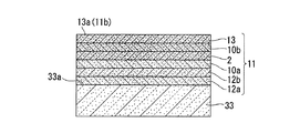
図1を参照するに、本発明の実施形態である発光ダイオード(LED)1は、発光層2を含む発光部3及び歪調整層13を少なくとも含む化合物半導体層11と、反射構造体4を介して発光部3に接合された機能性基板5である金属基板と、を有している。また、発光部3の反射構造体4と反対側の面3aには第1の電極6が備えられ、発光部3の反射構造体4側の面3bには、歪調整層13を介して、第2の電極8が備えられている。
Hereinafter, modes for carrying out the present invention will be described.
(First embodiment)
<Light emitting diode>
FIG. 1 is a diagram showing an example of a light emitting diode according to the first embodiment of the present invention.
Referring to FIG. 1, a light emitting diode (LED) 1 according to an embodiment of the present invention includes a
<発光部>
発光部3は、歪調整層13上に、少なくともp型の下部クラッド層10b、発光層2、n型の上部クラッド層10aが順次積層されて構成されている。すなわち、発光部3は、放射再結合をもたらすキャリア(担体;carrier)及び発光を発光層2に「閉じ込める」ために、発光層2の下側及び上側に対峙して配置した下部クラッド(clad)層10b及び上部クラッド層10aを含む、所謂、ダブルヘテロ(英略称:DH)構造とすることが高強度の発光を得る上で好ましい。
<Light emitting part>
The
図2は、本発明の第1の実施形態に係る発光ダイオードの発光部の構成を説明するための拡大断面図である。
図2を参照するに、発光層2は、歪発光層31と、バリア層32との多層構造であることが好ましい。
FIG. 2 is an enlarged cross-sectional view for explaining the configuration of the light emitting unit of the light emitting diode according to the first embodiment of the present invention.
Referring to FIG. 2, the
発光層2の層厚は、0.02〜2μmの範囲であることが好ましい。また、発光層2の伝導型は特に限定されるものではなく、アンドープ、p型及びn型のいずれも選択することができる。発光効率を高めるには、結晶性が良好なアンドープ又は3×1017cm−3未満のキャリア濃度とすることが望ましい。
The layer thickness of the
歪発光層31は、(AlXGa1−X)YIn1−YP(0≦X≦1,0<Y≦1)の組成を有している。上記Xは、0.1以下であることが好ましく、0であることがより好ましい。また、上記Yは、0.37〜0.46の範囲が好ましく、0.39〜0.45の範囲がより好ましい。歪発光層31の材質を上記範囲に規定することにより、発光波長を655〜675nmの範囲とすることできる。
しかしながら、この場合に歪発光層31は、それ以外の構造部分と格子定数が異なる構成となり、化合物半導体層2に歪が発生する。このため、結晶欠陥の発生という弊害が生ずるおそれがある。
The strained light-emitting
However, in this case, the strained
歪発光層31の層厚は、8〜30nmの範囲が好適である。ここで、歪発光層31の層厚が約6nm未満の薄膜である場合では、井戸構造の量子効果により発光波長が短くなり、所望の655nm以上が得られなくなる。
したがって、歪発光層31の層厚は、層厚の変動を加味して量子効果の発現しない8nm以上であることが望ましい。また、層厚の制御の容易さを考慮すれば、10nm以上が好適である。一方、歪発光層31の層厚が30nmを超えると、歪量が大きくなりすぎるため、結晶欠陥や表面の異常が発生しやすくなるために好ましくない。
The layer thickness of the strained
Therefore, the layer thickness of the strained
バリア層32は、(AlXGa1−X)YIn1−YP(0≦X≦1,0<Y≦1)の組成を有している。上記Xは、0.3〜0.7の範囲が好ましく、0.4〜0.6の範囲がより好ましい。また、上記Yは、0.48〜0.52の範囲が好ましく、0.49〜0.51の範囲がより好ましい。また、バリア層32の格子定数は、GaAs基板と同等または、小さくすることができる。
Barrier layer 32 has a composition of (Al X Ga 1-X) Y In 1-Y P (0 ≦ X ≦ 1,0 <Y ≦ 1). X is preferably in the range of 0.3 to 0.7, more preferably in the range of 0.4 to 0.6. Y is preferably in the range of 0.48 to 0.52, and more preferably in the range of 0.49 to 0.51. Further, the lattice constant of the
バリア層32の層厚は、歪発光層31の層厚よりも厚いことが好ましい。これにより、歪発光層31の発光効率を高くすることができる。また、バリア層32によって発光効率を最適化すると共に歪発光層31に発生した歪を緩和する必要がある。
したがって、バリア層32は、少なくとも、15nm以上の層厚とすることが好ましく、20nm以上の層厚がより好ましい。一方、バリア層32の層厚が、50nmを超えると発光波長の波長に近くなり、光の干渉、ブラッグ反射等、光学的な影響がでる。
したがって、バリア層32は、50nm以下の層厚とすることが好ましく、40nm以下の層厚がより好ましい。
上述したように、歪発光層31の層厚が薄く、バリア層32の層厚が厚いほうが、歪発光層31の歪をバリア層32によって吸収する効果が得られると共に、歪発光層31に結晶欠陥が発生しにくいという効果が得られる。
The
Therefore, the
Therefore, the
As described above, when the strained
歪発光層31とバリア層32との多層構造において、歪発光層31とバリア層32とを交互に積層する対の数は特に限定されるものではないが、8対以上40対以下であることが好ましい。すなわち、発光層2には、歪発光層31が8〜40層含まれていることが好ましい。
ここで、発光層2の発光効率が好適な範囲としては、歪発光層31が8層以上であることが好ましい。一方、歪発光層31及びバリア層32は、キャリア濃度が低いため、多くの対にすると順方向電圧(VF)が、増大してしまう。
In the multilayer structure of the strained
Here, as a suitable range of the light emitting efficiency of the
このため、40対以下であることが好ましく、30対以下であることがより好ましい。また、歪発光層31が有する歪は、GaAs基板(図示せず)と発光層2との格子定数が異なるため、発光層2中に発生するストレスである。このため、歪発光層31とバリア層32とを交互に積層する対の数、すなわち、発光層2に含まれる歪発光層31の層の数が前記範囲を超えると、発光層2が歪に耐えきれずに結晶欠陥が発生し、表面状態の悪化や発光効率低下等の問題が発生する。
For this reason, it is preferable that it is 40 pairs or less, and it is more preferable that it is 30 pairs or less. The strain of the strained
発光層2(発光部3)は、歪発光層31の材質を上記範囲に規定することにより、その発光スペクトルのピーク発光波長が655〜675nmの範囲とすることが好ましく、該範囲内でもより光合成の効率が高い660〜670nmの範囲とすることがより好ましい。上記範囲の発光波長は、植物育成(光合成)用の光源に適した発光波長の1つであり、光合成に対して反応効率が高いために望ましい。
一方、700nm以上の長波長領域の光を利用すると、植物の育成を抑制する反応が起こる為、長波長域の光量は少ない方が望ましい。従って、効率的に植物育成する為には、光合成反応に対して最適な655〜675nmの波長領域の光が強く、700nm以上の超波長領域の光を含まない赤色光源が最も好ましい。
The light-emitting layer 2 (light-emitting portion 3) preferably has a peak emission wavelength in the emission spectrum of 655 to 675 nm by defining the material of the strained light-emitting
On the other hand, when light in a long wavelength region of 700 nm or more is used, a reaction that suppresses plant growth occurs. Therefore, it is desirable that the amount of light in the long wavelength region is small. Therefore, in order to grow plants efficiently, a red light source that has strong light in the wavelength region of 655 to 675 nm, which is optimal for the photosynthetic reaction, and does not contain light in the super wavelength region of 700 nm or more is most preferable.
また、前記の好ましい赤色光源にする為には、半値幅は、狭い必要がある。一方、波長バラツキの大きくなる可能性がある量子化条件に近いと半値幅が狭くなる為、結果的に発光スペクトルの半値幅が、10〜40nmの範囲であることが好ましい。
さらに、上記発光スペクトルの発光波長700nmにおける発光強度が、上記ピーク発光波長における発光強度の10%未満であることが好ましい。また、発光層2の応答速度(立ち上がり時間:Tr)を100ns以下であることが好ましい。
このような特性の発光層2を有する発光ダイオード1は、植物育成の光合成の促進に使用する照明(発光ダイオードランプ)として好適に用いることができる。また、発光層2の構成は、上記特性を充足するように組成、層厚、層数を適宜選択することができる。
Further, in order to obtain the preferable red light source, the half width needs to be narrow. On the other hand, since the half-value width is narrowed near the quantization condition that may cause wavelength variation, the half-value width of the emission spectrum is preferably in the range of 10 to 40 nm.
Furthermore, it is preferable that the emission intensity of the emission spectrum at an emission wavelength of 700 nm is less than 10% of the emission intensity at the peak emission wavelength. Moreover, it is preferable that the response speed (rise time: Tr) of the
The
図1を参照するに、下部クラッド層10b及び上部クラッド層10aは、発光層2のいずれか一方の面に設けられている。具体的には、発光層2の下面に下部クラッド層10bが設けられ、発光層2の上面に上部クラッド層10aが設けられている。
Referring to FIG. 1, the
下部クラッド層10b及び上部クラッド層10aの材質としては、歪発光層31よりもバンドギャップの大きい材質が好ましく、バリア層32よりもバンドギャップが大きい材質がより好ましい。
上記材質としては、例えば、AlXGa1−XAsの組成を有する化合物や、(AlXGa1−X)YIn1−YP(0≦X≦1,0<Y≦1)の組成を有する化合物が挙げられる。上記Xの値は、下限値が0.3以上であることが好ましく、0.5以上であることがより好ましい。また、上記Yの値は、0.48〜0.52の範囲が好ましく、0.49〜0.51の範囲がより好ましい。
The material of the
Examples of the material include a compound having a composition of Al X Ga 1-X As, and a composition of (Al X Ga 1-X ) Y In 1-YP (0 ≦ X ≦ 1, 0 <Y ≦ 1). The compound which has is mentioned. The lower limit of the value of X is preferably 0.3 or more, and more preferably 0.5 or more. The value of Y is preferably in the range of 0.48 to 0.52, and more preferably in the range of 0.49 to 0.51.
下部クラッド層10bと上部クラッド層10aとは、極性が異なるように構成されている。また、下部クラッド層10b及び上部クラッド層10aのキャリア濃度及び厚さは、公知の好適な範囲を用いることができ、発光層2の発光効率が高まるように条件を最適化することが好ましい。また、下部クラッド層10b及び上部クラッド層10aの組成を制御することによって、化合物半導体層11の反りを低減させることができる。
The
具体的に、下部クラッド層10bとしては、例えば、Mgをドープしたp型の(AlXGa1−X)YIn1−YP(0.3≦X≦1,0<Y≦1)よりなる半導体材料を用いることが望ましい。また、キャリア濃度は2×10¹⁷〜2×1018cm−3の範囲が好ましく、層厚は0.5〜5μmの範囲が好ましい。
Specifically, as the
一方、上部クラッド層10aとしては、例えば、Siをドープしたn型の(AlXGa1−X)YIn1−YP(0.3≦X≦1,0<Y≦1)よりなる半導体材料を用いることが望ましい。
また、キャリア濃度は1×10¹⁷〜1×1018cm−3の範囲が好ましく、層厚は0.5〜2μmの範囲が好ましい。なお、下部クラッド層10b及び上部クラッド層10aの極性は、化合物半導体層11の素子構造を考慮して選択することができる。
On the other hand, the
The carrier concentration is preferably in the range of 1 × 10 17 to 1 × 10 18 cm −3 , and the layer thickness is preferably in the range of 0.5 to 2 μm. The polarities of the lower
上部クラッド層10aのコンタクト層12bと接触する面は、光取り出し面11aとして機能する面であり、粗面化されている(言い換えれば、粗い面を含んでいる)。
このように、光取り出し面11aを粗面化することにより、光取り出し面11aでの全反射が抑制されるため、光取り出し効率を向上させることができる。
The surface of the
As described above, by roughening the
また、下部クラッド層10bと発光層2との間、発光層2と上部クラッド層10aとの間及び上部クラッド層10aと歪調整層13との間に、両層間におけるバンド(band)不連続性を緩やかに変化させるための中間層を設けても良い。この場合、各中間層は、上記両層の中間の禁止帯幅を有する半導体材料からそれぞれ構成することが好ましい。
Band discontinuities between the
また、発光部3の構成層の最上層には、オーミック(Ohmic)電極の接触抵抗を下げるためのコンタクト層12bが設けられている。
なお、コンタクト層12bの他に、素子駆動電流を発光部の全般に平面的に拡散させるための電流拡散層、逆に素子駆動電流の通流する領域を制限するための電流阻止層や電流狭窄層等、公知の層構造を設けてもよい。
In addition, a
In addition to the
<歪調整層>
図1を参照するに、歪調整層13は、発光部3の下方に設けられている。この歪調整層13は、GaAs基板(図示せず)上に化合物半導体層11をエピタキシャル成長させる際に、歪発光層31によって生じた歪を緩和させるための層である。また、歪調整層13は、発光部3の発光波長に対して透明である。
さらに、歪調整層13は、歪発光層31及びバリア層32の格子定数よりも小さい格子定数を有している。また、歪調整層13は、化合物半導体層11の形成(エピタキシャル成長による形成)に用いたGaAs基板(図示せず)の格子定数よりも小さい格子定数を有する。
より具体的には、後述する組成から得られる歪調整層13の格子定数をA、バリア層32の格子定数をB、歪発光層31の格子定数をCとした場合に、A<B<Cとなる関係を有している。
<Strain adjustment layer>
Referring to FIG. 1, the
Further, the
More specifically, when the lattice constant of the
歪調整層13としては、(AlXGa1−X)YIn1−YP(0≦X≦1、0.6≦Y≦1)の組成を有する材料を適用することが可能である。上記Xは、化合物半導体層11の素子構造にもよるが、Al濃度が低い材料が化学的に安定であることから、0.5以下であることが好ましく、0であることがより好ましい。
また、上記Yの下限値は、0.6以上であることが好ましい。ここで、発光層2(歪発光層31)の有する歪量が同じ場合を比較すると、上記Yの値が小さいほうが歪調整層13の歪調整効果が小さくなる。
このため、歪調整層13の層厚を厚くする必要が生じる。これにより、歪調整層13の成膜時の成長時間とコストが上昇してしまうため、上記Yの値は0.6以上であることが好ましく、0.8以上であることがより好ましい。
As the
Moreover, it is preferable that the said lower limit of Y is 0.6 or more. Here, when the amount of strain of the light emitting layer 2 (strained light emitting layer 31) is the same, the strain adjusting effect of the
For this reason, it is necessary to increase the thickness of the
また、歪調整層13としては、発光部3の発光波長に対して透明な層であり、AlXGa1−XAs1−YPY(0≦X≦1、0.6≦Y≦1)の組成を有するIII−V属半導体材料も好適に用いることができる。
上記組成を有する歪調整層13では、Yの値によって格子定数が変化する。上記Yの値が大きい方が、格子定数が小さくなる。また、発光部3の光を透過させるか否かは、上記X及びYの値の双方に関連する為、発光部3の発光波長に対して透明なようにX及びYの値を選択すれば良い。
Further, the
In the
さらに、歪調整層13として、GaP層、好ましくは、例えばMgドープしたp型のGaP層を用いることが好ましい。GaP層は、組成の調整が不要であると共に歪調整効果が大きいため、生産性及び安定性の面からも歪調整層13として最も適している。
Further, as the
歪調整層13は、発光部3をエピタキシャル成長させる際に用いる基板であるGaAs基板(図示せず)の格子定数よりも小さい格子定数を有しているため、歪発光層31が包含する歪量のばらつきを緩和する機能を備えている。
このため、歪調整層13を設けることにより、発光波長等の特性の均一化、クラック発生等の結晶欠陥の発生防止の効果がある。
ここで、歪調整層13の厚さは、0.5〜20μmの範囲であることが好ましく、3〜15μmの範囲であることがより好ましい。層厚が0.5μm未満であると、歪発光層31の歪量のばらつきを緩和するのに十分ではなく、層厚が20μmを超えると成長時間が長くなり、製造コストが増加するので好ましくない。
Since the
For this reason, the provision of the
Here, the thickness of the
このように、歪調整層13の組成を制御することにより、化合物半導体層11の反りを低減できるため、面内波長分布の小さい発光ダイオード1の作製が可能である。
さらに、本実施形態のように、反射構造体4を介して、機能性基板5と化合物半導体層11との接合を行なう構造を有する場合にも、化合物半導体層11の反りが大きい場合は割れ等の問題が生じるため、化合物半導体層11の反りを小さくすることが望ましい。
Thus, by controlling the composition of the
Further, even when the
<第1の電極、第2の電極>
第1の電極6及び第2の電極8は、それぞれオーミック電極であり、それらの形状及び配置は、発光部3に電流を均一に拡散させるものであればよく、特に限定されない。例えば、平面視したときに円状または矩形状の電極を用いることができ、一個の電極として配置することも、複数の電極を格子状に配置することもできる。
<First electrode, second electrode>
The
第1の電極6の材料としては、コンタクト層12bとしてn型の化合物半導体を用いた場合には、例えば、AuGe層、AuSi層等を用いることができ、コンタクト層12bとしてp型の化合物半導体を用いた場合には、例えば、AuBe層、AuZn層等を用いることができる。
また、更にその上にAu層等を積層することで、酸化を防止させると共に、ワイヤボンディングの接続信頼性を向上できる。
As the material of the
Further, by further laminating an Au layer or the like thereon, oxidation can be prevented and connection reliability of wire bonding can be improved.
第2の電極8の材料としては、歪調整層13としてn型の化合物半導体を用いた場合には、例えば、AuGe層、AuSi層等を用いることができ、歪調整層13としてp型の化合物半導体を用いた場合には、例えば、AuBe層、AuZn層等を用いることができる。
As the material of the
<反射構造体>
図1を参照するに、反射構造体4は、第2の電極8を覆うように、歪調整層13の面13aに形成されている。反射構造体4は、透明導電膜14と、反射層15とが順次積層された構成とされている。
<Reflection structure>
Referring to FIG. 1, the
透明導電膜14は、第2の電極8を覆うように、歪調整層13の面13a(第2の電極8が形成された歪調整層13の面)に形成されている。透明導電膜14としては、例えば、ITO膜、IZO膜等を用いることができる。
また、透明導電膜14の代わりに、或いは、透明導電膜14と共に、透明な材料の屈折率差を利用したいわゆるコールドミラー、例えば、酸化チタン膜、酸化ケイ素膜の多層膜や白色のアルミナ、AlNを用いて、反射層15に組み合わせてもよい。
The transparent
Further, instead of the transparent
図1を参照するに、反射層15は、透明導電膜14に積層されている。反射層15は、銅、銀、金、アルミニウム等の金属及びそれらの合金等の材料により構成されている。これらの材料は光反射率が高く、反射構造体4からの光反射率を90%以上とすることができる。
このような反射層15を設けることにより、発光層2からの光を反射層15で正面方向fへ反射させて、正面方向fでの光取り出し効率を向上させることができる。これにより、発光ダイオード1をより高輝度化できる。
なお、ここでの正面方向fとは、化合物半導体層11の光取り出し面11a(本実施形態の場合、発光部3の面3a)との成す角度が90°となる方向で、かつ発光ダイオード1のから離間する方向のことをいう。なお、反射構造体4は、透明導電膜14を設けることなく、反射層15だけで構成してもよい。
Referring to FIG. 1, the
By providing such a
Here, the front direction f is a direction in which the angle formed by the
また、反射構造体4は、光取り出し面11aに対して90°の角度を成す方向に放射される放射照度が、光取り出し面11aに対して45°の角度を成す方向に放射される放射照度の1.0倍よりも大きくなるように構成するとよい。
このように、光取り出し面11aに対して90°の角度を成す方向(光取り出し面11aに対して直交する方向)に放射される放射照度を、光取り出し面11aに対して45°の角度を成す方向に放射される放射照度の1.0倍よりも大きくすることにより、高輝度及び高効率の発光ダイオード1を実現できる。
また、光取り出し面11aに対して直交する方向における光の強度を強くすることにより、光取り出し面11aに対して直交する方向において、反射構造体4を備えていない発光ダイオードの光の強度と同じ強さの光強度を得る場合、反射構造体4を備えていない発光ダイオードよりも消費電力を小さくすることができる。
Further, in the reflecting
Thus, the irradiance radiated in the direction that forms an angle of 90 ° with respect to the
Further, by increasing the intensity of light in the direction orthogonal to the
図3は、反射構造体を備えていない発光ダイオード及び反射構造体を備えた発光ダイオードの放射照度を示す図である。図3では、光取り出し面11aから照射された光の放射照度を示している。また、図3では、光取り出し面11aに対して直交する方向の照射角度を90°とし、光取り出し面11aに対して平行な方向の照射角度を0°とする。
FIG. 3 is a diagram showing the irradiance of a light emitting diode not provided with a reflective structure and a light emitting diode provided with a reflective structure. In FIG. 3, the irradiance of the light irradiated from the
図3を参照するに、反射構造体4を備えていない発光ダイオードでは、斜め方向(具体的には、放射角度が15〜55°の方向)において放射照度が大きく、放射角度が60°から90°に近づくにつれて、放射照度が小さくなることが確認できる。
一方、反射構造体4を備えた発光ダイオード1では、放射角度が60°以下において、反射構造体4を備えていない発光ダイオードよりも放射照度が小さく、放射角度が60°〜90°の範囲内において、反射構造体4を備えていない発光ダイオードよりも照射照度が大きくなることが確認できた。
このことから、反射構造体4を設けることで、光取り出し面11aに対して90°の角度を成す方向に放射される光の放射照度を強くできることが確認できた。
Referring to FIG. 3, in the light emitting diode not provided with the reflecting
On the other hand, in the
From this, it was confirmed that the provision of the
具体的には、反射層15としては、例えば、透明導電膜14側からAg合金層/W層/Pt層/Au層/接続用金属層よりなる積層膜を用いることができる。透明導電膜14と接触する面とは反対側に位置する反射層15の面15bに形成された前記接続用金属としては、電気抵抗が低く、低温で溶融する金属を用いるとよい。このような接続用金属を用いることにより、発光部3に熱ストレスを与えることなく、機能性基板5を接続できる。
上記接続用金属としては、化学的に安定で、融点の低いAu系の共晶金属等を用いるとよい。前記Au系の共晶金属としては、例えば、AuSn、AuGe、AuSi等の合金の共晶組成(Au系の共晶金属)を挙げることができる。
また、接続用金属には、チタン、クロム、タングステン等の金属を添加することが好ましい。接続用金属としてチタン、クロム、タングステン等の金属を添加することにより、該金属がバリヤ金属として機能するため、機能性基板5に含まれる不純物等が反射層15側に拡散して、反応することを抑制できる。
Specifically, as the
As the connection metal, an Au-based eutectic metal that is chemically stable and has a low melting point may be used. Examples of the Au-based eutectic metal include eutectic compositions (Au-based eutectic metals) of alloys such as AuSn, AuGe, and AuSi.
Moreover, it is preferable to add metals, such as titanium, chromium, and tungsten, to the connection metal. By adding a metal such as titanium, chromium or tungsten as a connecting metal, the metal functions as a barrier metal, so that impurities contained in the
<機能性基板(金属基板)>
図1を参照するに、機能性基板5は、反射構造体4を介して、化合物半導体層11の面11b(具体的には、歪調整層13の面13a)に貼り付けられている。具体的には、発光部3と対向する反射構造体4の面とは反対側に位置する反射構造体4の面15bに、機能性基板5の接合面5aが接合されている。
<Functional substrate (metal substrate)>
Referring to FIG. 1, the
第1の実施形態では、機能性基板5として金属基板を用いる。つまり、第1の実施形態では、反射構造体4を介して、化合物半導体層11の面11b(具体的には、歪調整層13の面13a)に、金属基板が貼り付けられている。以下、機能性基板5として金属基板を用いた場合を例に挙げて説明する。
In the first embodiment, a metal substrate is used as the
機能性基板5は、複数の金属層からなるものを用いることができる。さらに、機能性基板5は、2種類の金属層を交互に積層して構成することが好ましい。また、上記2種類の金属層の合計の層数は、奇数とすることが好ましい。
The
この場合、機能性基板5の反りや割れの観点から、第2の金属層22として化合物半導体層11より熱膨張係数が小さい材料を用いる場合、第1の金属層21を化合物半導体層11より熱膨張係数が大きい材料で構成することが好ましい。
これにより、機能性基板5全体としての熱膨張係数が化合物半導体層11の熱膨張係数に近くなるため、化合物半導体層11と機能性基板5とを接合する際の機能性基板5の反りや割れを抑制することが可能となるので、発光ダイオード1の歩留まりを向上できる。
In this case, from the viewpoint of warping and cracking of the
Thereby, since the thermal expansion coefficient of the
また、第2の金属層22として化合物半導体層11より熱膨張係数が大きい材料を用いる場合、第1の金属層21を化合物半導体層11より熱膨張係数が小さい材料で構成することが好ましい。
これにより、機能性基板5全体としての熱膨張係数が、化合物半導体層11の熱膨張係数に近くなるため、化合物半導体層11と機能性基板5とを接合する際の機能性基板5の反りや割れを抑制することが可能となるので、発光ダイオード1の歩留まりを向上できる。
In addition, when a material having a larger thermal expansion coefficient than the
As a result, the thermal expansion coefficient of the
以上説明したように、機能性基板5を構成する第1及び第2の金属層21,22の位置は、入れ替えることが可能である。つまり、図1では、2つの第1の金属層21が1つの第2の金属層を挟み込むことで機能性基板5を構成しているが、2つの第2の金属層22により1つの第1の金属層21を挟みこむことで機能性基板5(金属基板)を構成してもよい。
As described above, the positions of the first and second metal layers 21 and 22 constituting the
第1及び第2の金属層21,22よりなる機能性基板5は、例えば、銀(熱膨張係数=18.9ppm/K)、銅(熱膨張係数=16.5ppm/K)、金(熱膨張係数=14.2ppm/K)、アルミニウム(熱膨張係数=23.1ppm/K)、ニッケル(熱膨張係数=13.4ppm/K)、及びこれらの合金のうち、いずれかの材料よりなる金属層と、モリブデン(熱膨張係数=5.1ppm/K)、タングステン(熱膨張係数=4.3ppm/K)、クロム(熱膨張係数=4.9ppm/K)、及びこれらの合金のうち、いずれかの材料よりなる金属層との組み合わせで構成できる。
The
機能性基板5(金属基板)の好適な例としては、Cu層/Mo層/Cu層の3層よりなる金属基板が挙げられる。先に説明したように、Mo層/Cu層/Mo層の3層よりなる金属基板でも、Cu層/Mo層/Cu層の3層よりなる金属基板と同様な効果を得ることが可能である。
一方、Cu層/Mo層/Cu層の3層よりなる金属基板は、機械的強度の高いMoを加工しやすいCuで挟んだ構造であるため、Mo層/Cu層/Mo層の3層よりなる金属基板よりも金属基板の切断等の加工を容易に行なうことができるという利点がある。
A suitable example of the functional substrate 5 (metal substrate) is a metal substrate composed of three layers of Cu layer / Mo layer / Cu layer. As described above, even a metal substrate composed of three layers of Mo layer / Cu layer / Mo layer can achieve the same effect as a metal substrate composed of three layers of Cu layer / Mo layer / Cu layer. .
On the other hand, a metal substrate composed of three layers of Cu layer / Mo layer / Cu layer has a structure in which Mo having high mechanical strength is sandwiched between Cu, which is easy to process. There is an advantage that processing such as cutting of the metal substrate can be performed more easily than the metal substrate.
機能性基板5全体としての熱膨張係数は、例えば、機能性基板5としてCu層(30μm)/Mo層(25μm)/Cu層(30μm)よりなる金属基板を用いた場合、6.1ppm/Kとなる。また、機能性基板5としてMo層(25μm)/Cu層(70μm)/Mo層(25μm)よりなる金属基板を用いた場合、例えば、機能性基板5全体としての熱膨張係数は5.7ppm/Kとなる。
The thermal expansion coefficient of the
また、放熱の観点からは、機能性基板5を構成する金属層は熱伝導率が高い材料よりなることが好ましい。このような材料を用いることにより、機能性基板5の放熱性を高くすることが可能となり、発光ダイオード1を高輝度で発光させることができると共に、発光ダイオード1の寿命を長寿命とすることができる。
From the viewpoint of heat dissipation, the metal layer constituting the
上記熱伝導率が高い材料としては、例えば、銀(熱伝導率=420W/m・K)、銅(熱伝導率=398W/m・K)、金(熱伝導率=320W/m・K)、アルミニウム(熱伝導率=236W/m・K)、モリブデン(熱伝導率=138W/m・K)、タングステン(熱伝導率=174W/m・K)、及びこれらの合金等を用いることが好ましい。 Examples of the material having high thermal conductivity include silver (thermal conductivity = 420 W / m · K), copper (thermal conductivity = 398 W / m · K), and gold (thermal conductivity = 320 W / m · K). Aluminum (thermal conductivity = 236 W / m · K), molybdenum (thermal conductivity = 138 W / m · K), tungsten (thermal conductivity = 174 W / m · K), and alloys thereof are preferably used. .
さらに、機能性基板5を構成する金属層の熱膨張係数が、化合物半導体層11の熱膨張係数と略等しい材料よりなることが好ましい。
特に、機能性基板5を構成する金属層の材料の熱膨張係数が、化合物半導体層11の熱膨張係数の±1.5ppm/K以内であることが好ましい。これにより、機能性基板5と化合物半導体層11との接合時に発生する発光部3へのストレス(熱に起因するストレス)を小さくすることが可能となり、機能性基板5と化合物半導体層11と接続させた際の熱による機能性基板5の割れが抑制されるので、発光ダイオード1の歩留まりを向上できる。
Further, the thermal expansion coefficient of the metal layer constituting the
In particular, the thermal expansion coefficient of the material of the metal layer constituting the
機能性基板5としてCu層(30μm)/Mo層(25μm)/Cu層(30μm)よりなる金属基板を用いた場合、機能性基板5の熱伝導率は250W/m・Kとなる。
また、機能性基板5としてMo層(25μm)/Cu層(70μm)/Mo層(25μm)よりなる金属基板を用いた場合、機能性基板5の熱伝導率は220W/m・Kとなる。
When a metal substrate composed of a Cu layer (30 μm) / Mo layer (25 μm) / Cu layer (30 μm) is used as the
When a metal substrate composed of Mo layer (25 μm) / Cu layer (70 μm) / Mo layer (25 μm) is used as the
金属基板よりなる機能性基板5の厚さは、50μm以上150μm以下とすることが好ましい。
機能性基板5の厚さが150μmより厚い場合には、発光ダイオードの製造コストが上昇して好ましくない。また、機能性基板5の厚さが50μmより薄い場合には、ハンドリング時に割れ、欠け、反り等が容易に生じて、発光ダイオードの歩留まりを低下させる虞がある。
The thickness of the
When the thickness of the
1枚の機能性基板5を構成する第1の金属層21及び第2の金属層22の層数は、合わせて3〜9層とすることが好ましく、3〜5層とすることがより好ましい。
第1の金属層21と第2の金属層22の層数を合わせて2層とした場合には、厚さ方向での熱膨張が不均衡となり、機能性基板5の割れが発生するおそれが発生する。逆に、第1の金属層21と第2の金属層22の層数を合わせて9層より多くした場合には、第1の金属層21と第2の金属層22の層の厚さをそれぞれ薄くする必要が生じる。
The number of
When the number of layers of the
しかしながら、第1及び第2の金属層21,22の厚さを薄く作製することは非常に困難であるため、第1の金属層21或いは第2の金属層22の厚さを薄くして、単層の金属基板を形成した場合、各層の厚さが不均一となり、発光ダイオードの特性をばらつかせる虞がある。
さらに、層の厚さを薄くした前記単層の金属基板は、容易に基板の割れを発生させる。また、薄膜化された単層の金属基板を用いる場合、金属基板の製造が困難であることから、発光ダイオードの製造コストを増加させる虞がある。
However, since it is very difficult to make the first and second metal layers 21 and 22 thin, the
Furthermore, the single-layer metal substrate having a thin layer thickness easily causes the substrate to crack. In addition, when a thin single-layer metal substrate is used, it is difficult to manufacture the metal substrate, which may increase the manufacturing cost of the light emitting diode.
なお、機能性基板5の接合面5aに、電気的接触を安定化させる接合補助膜、または、ダイボンド用の共晶金属を形成してもよい。これにより、接合工程を簡便に行うことができる。前記接合補助膜としては、Au膜、AuSn膜等を用いることができる。
A bonding auxiliary film that stabilizes electrical contact or a eutectic metal for die bonding may be formed on the
なお、発光部3に機能性基板5を接合する方法は、上記に記載した方法に限られるものではなく、例えば、拡散接合、接着剤、常温接合方法等公知の技術を適用できる。
The method for bonding the
第1の実施形態の発光ダイオード1によれば、pn接合型の発光部3と、発光部3に積層された歪調整層8と、を少なくとも含む化合物半導体層11を備え、発光部3を、組成式(AlXGa1−X)YIn1−YP(0≦X≦0.1、0.37≦Y≦0.46)よりなる歪発光層31とバリア層32との積層構造とすることにより、発光部3から放射される光の発光効率及び応答速度を向上できる。
また、歪発光層31の組成を上記範囲に規定することにより、655nm以上の発光波長を有した発光ダイオード1を実現できる。
また、発光部3上に、発光部3の光を透過させる歪調整層13を設けることにより、歪調整層13により発光部3からの光が吸収されることがないため、高出力・高効率の発光ダイオード1を実現できる。
According to the
Further, by defining the composition of the strained
Further, by providing the
さらに、この歪調整層13は、歪発光層31及びバリア層32の格子定数よりも小さい格子定数を有しているため、半導体化合物層11の反りの発生を抑制できる。これにより、歪発光層31の歪量のばらつきが低減されるため、単色性に優れた発光ダイオード1を実現できる。
また、化合物半導体層11の光取り出し面11aとは反対側に位置する化合物半導体層11の面11bに、反射構造体4を設けることにより、化合物半導体層11の光取り出し面11aから発光ダイオード1の外部に放射される光のうち、光取り出し面11aに対して直交する方向(具体的には、正面方向f)における光の強度を強くすることが可能となるので、高輝度及び高効率の発光ダイオード1を実現できる。
また、光取り出し面11aに対して直交する方向における光の強度を強くすることにより、光取り出し面11aに対して直交する方向において、反射構造体4を備えていない発光ダイオードの光の強度と同じ強さの光強度を得る場合、反射構造体4を備えていない発光ダイオードよりも消費電力を小さくすることができる。
Furthermore, since the
Further, the
Further, by increasing the intensity of light in the direction orthogonal to the
また、例えば、化合物半導体層11の面11bに、反射構造体14を介して接合される機能性基板5として金属基板を用いることにより、発光部3が発光した際の熱を、機能性基板5を介して、発光ダイオード1の外部に効率良く放出することができる。
さらに、熱伝導率が130W/m・K以上である第1及び第2の金属層21,22により機能性基板5を構成することで、機能性基板5の放熱性が高くなるため、発光ダイオード1を高輝度で発光させることができると共に、発光ダイオード1の寿命を長寿命とすることができる。
また、機能性基板5として光を透過する基板を用いて、Arビームにより接合させた場合、接合面が高抵抗となり、基板側へ電流を流すことが難しいが、機能性基板5として金属基板を用いて、該金属基板を共晶接合させることにより、1ワイヤー構造の作成が可能となる。
Further, for example, by using a metal substrate as the
Further, since the
In addition, when a light-transmitting substrate is used as the
つまり、第1の実施形態の発光ダイオードによれば、655nm以上の赤色光の発光波長を有し、単色性に優れると共に、高出力・高効率であって応答速度が速く、かつ光取り出し面に対して直交する方向における光強度が強く、さらに放熱特性に優れた発光ダイオード1を実現できる。
That is, according to the light emitting diode of the first embodiment, it has a red light emission wavelength of 655 nm or more, is excellent in monochromaticity, has high output and high efficiency, has a high response speed, and has a light extraction surface. On the other hand, it is possible to realize the
<発光ダイオードの製造方法>
次に、第1の実施形態である発光ダイオード1の製造方法について説明する。
第1の実施形態である発光ダイオード1の製造方法は、機能性基板5を形成する工程と、次いで、半導体基板33にコンタクト層12bを介して発光層2を含む発光部3を形成した後、発光部3の半導体基板33と反対側の面に第2の電極8を形成する工程と、発光部3の半導体基板と反対側の面に第2の電極8を介して反射構造体4を形成する工程と、発光部3に反射構造体4を介して機能性基板5を接合する工程と、半導体基板33、及びコンタクト層12bの一部を除去する工程と、発光部3の機能性基板5と反対側の面に第1の電極6を形成する工程と、を有する。
<Method for manufacturing light-emitting diode>
Next, the manufacturing method of the
In the method of manufacturing the light-emitting
図4〜図10は、本発明の第1の実施形態に係る発光ダイオードの製造工程を示す断面図である。図4〜図10において、図1に示す発光ダイオード1と同一構成部分には、同一符号を付す。
図4〜図10を参照して、第1の実施形態の発光ダイオード1の製造方法について説明する。まず、機能性基板5の製造工程について説明する。
4-10 is sectional drawing which shows the manufacturing process of the light emitting diode which concerns on the 1st Embodiment of this invention. 4-10, the same code | symbol is attached | subjected to the same component as the
With reference to FIGS. 4-10, the manufacturing method of the
<機能性基板の製造工程>
図4に示すように、機能性基板5は、熱伝導率が130W/m・K以上である第1及び第2の金属層21,22をホットプレスすることで形成する。
<Manufacturing process of functional substrate>
As shown in FIG. 4, the
具体的には、まず、2枚の略平板状の第1の金属層21と、1枚の略平板状の第2の金属層22を用意する。例えば、第1の金属層21としては厚さ30μmのCu層を用い、第2の金属層22としては厚さ25μmのMo層を用いる。
次に、図4(a)に示すように、2枚の第1の金属層21の間に第2の金属層22を挿入してこれらを重ねて配置する。
Specifically, first, two substantially flat plate-like
Next, as shown in FIG. 4A, the
次に、所定の加圧装置内に、第1及び第2の金属層21,22が積み重ねられた積層板を配置して、高温下で、第1の金属層21と第2の金属層22に矢印の方向(図4(a)参照)に荷重をかけて圧着する。
これにより、図4(b)に示すように、第1の金属層21がCu層であり、第2の金属層22がMo層であり、Cu層(30μm)/Mo層(25μm)/Cu層(30μm)の3層よりなる機能性基板5を形成する。上記構成とされた機能性基板5の熱膨張係数は、6.1ppm/Kであり、熱伝導率は250W/m・Kであった。
Next, a laminated plate in which the first and second metal layers 21 and 22 are stacked is disposed in a predetermined pressurizing apparatus, and the
As a result, as shown in FIG. 4B, the
なお、この後、発光部3(ウェーハ)の接合面の大きさに合わせて切断した後、表面を鏡面加工してもよい。
また、機能性基板5の接合面5aに、電気的接触を安定化させるため接合補助膜を形成してもよい。該接合補助膜としては、金膜、白金膜、ニッケル膜等を用いることができる。例えば、まず、ニッケル膜を0.1μm成膜した後、ニッケル膜上に金膜を0.5μm成膜する。
さらにまた、上記接合補助膜の代わりに、ダイボンド用のAuSn膜等の共晶金属膜を形成してもよい。これにより、接合工程を簡便にすることができる。
In addition, after this, after cutting according to the magnitude | size of the joint surface of the light emission part 3 (wafer), you may mirror-finish the surface.
Further, a bonding auxiliary film may be formed on the
Furthermore, a eutectic metal film such as an AuSn film for die bonding may be formed instead of the above-mentioned bonding auxiliary film. Thereby, a joining process can be simplified.
<発光部及び第2の電極形成工程>
まず、図5に示すように、半導体基板33の表面33a上に、複数のエピタキシャル層を成長させて化合物半導体層11を形成する。なお、この段階では、化合物半導体層11を構成するコンタクト層12bは、パターニングされていない。
半導体基板33は、化合物半導体層11を形成するための基板であり、例えば、表面33aが(100)面から15°傾けた面とされ、かつSiドープされたn型のGaAs単結晶基板である。このように、化合物半導体層11としてAlGaInP層またはAlGaAs層を用いる場合、化合物半導体層11を形成する基板としては、砒化ガリウム(GaAs)単結晶基板を用いるとよい。
<Light emitting portion and second electrode forming step>
First, as shown in FIG. 5, a plurality of epitaxial layers are grown on the
The
化合物半導体層11は、半導体基板33であるGaAs基板上に、GaAsよりなる緩衝層12a、選択エッチングに利用するために設けられたエッチングストップ層(図示せず)、Siをドープしたn型のAlGaInPよりなるコンタクト層12b、n型の上部クラッド層10a、発光層2、p型の下部クラッド層10b、及びMgドープしたp型GaPよりなる歪調整層13を順次積層して作製する。
The
GaAs基板は、公知の製法で作製された市販品の単結晶基板を使用できる。GaAs基板のエピタキシャル成長させる表面は、平滑であることが望ましい。GaAs基板の表面の面方位は、エピ成長しやすく、量産されている(100)面及び(100)から、±20°以内にオフした基板が、品質の安定性の面からのぞましい。
さらに、GaAs基板の面方位の範囲が、(100)方向から(0−1−1)方向に15°オフ±5°であることがより好ましい。
As the GaAs substrate, a commercially available single crystal substrate manufactured by a known manufacturing method can be used. The surface on which the GaAs substrate is epitaxially grown is preferably smooth. The surface orientation of the surface of the GaAs substrate is easily epi-grown, and from the (100) plane and (100) that are mass-produced, a substrate that is turned off within ± 20 ° is preferred from the standpoint of quality stability.
Furthermore, the range of the plane orientation of the GaAs substrate is more preferably 15 ° off ± 5 ° from the (100) direction to the (0-1-1) direction.
GaAs基板の転位密度は、化合物半導体層11の結晶性を良くするために低い方が望ましい。具体的には、例えば、10,000個cm−2以下、望ましくは、1,000個cm−2以下であることが好適である。
The dislocation density of the GaAs substrate is desirably low in order to improve the crystallinity of the
GaAs基板は、n型であってもp型であっても良い。GaAs基板のキャリア濃度は、所望の電気伝導度と素子構造から、適宜選択することができる。
例えば、GaAs基板がシリコンドープのn型である場合には、キャリア濃度が1×10¹⁷〜5×1018cm−3の範囲であることが好ましい。これに対して、GaAs基板が亜鉛をドープしたp型の場合には、キャリア濃度2×10¹⁸〜5×1019cm−3の範囲であることが好ましい。
The GaAs substrate may be n-type or p-type. The carrier concentration of the GaAs substrate can be appropriately selected from desired electrical conductivity and element structure.
For example, when the GaAs substrate is a silicon-doped n-type, the carrier concentration is preferably in the range of 1 × 10 17 to 5 × 10 18 cm −3 . On the other hand, when the GaAs substrate is a p-type doped with zinc, the carrier concentration is preferably in the range of 2 × 10 18 to 5 × 10 19 cm −3 .
GaAs基板の厚さは、基板のサイズに応じて適切な範囲がある。GaAs基板の厚さが適切な範囲よりも薄いと、化合物半導体層11の製造プロセス中に割れてしまう虞がある。
一方、GaAs基板の厚さが適切な範囲よりも厚いと材料コストが増加することになる。このため、GaAs基板の基板サイズが大きい場合、例えば、直径75mmの場合には、ハンドリング時の割れを防止するために250〜500μmの厚さが望ましい。
同様に、直径50mmの場合は、200〜400μmの厚さが望ましく、直径100mmの場合は、350〜600μmの厚さが望ましい。
The thickness of the GaAs substrate has an appropriate range depending on the size of the substrate. If the thickness of the GaAs substrate is thinner than an appropriate range, the
On the other hand, if the thickness of the GaAs substrate is thicker than an appropriate range, the material cost increases. For this reason, when the substrate size of the GaAs substrate is large, for example, when the diameter is 75 mm, a thickness of 250 to 500 μm is desirable to prevent cracking during handling.
Similarly, when the diameter is 50 mm, a thickness of 200 to 400 μm is desirable, and when the diameter is 100 mm, a thickness of 350 to 600 μm is desirable.
このように、GaAs基板の基板サイズに応じて基板の厚さを厚くすることにより化合物半導体層11の反りを低減することができる。これにより、エピタキシャル成長中の温度分布が均一となることため、発光層2の面内の波長分布を小さくすることができる。なお、GaAs基板の形状は、特に円形に限定されず、矩形等であっても問題ない。
Thus, the warp of the
緩衝層12aは、半導体基板33と発光部3の構成層との格子ミスマッチの緩和するために設けられている。このため、基板の品質やエピタキシャル成長条件を選択すれば、緩衝層12aは、必ずしも必要ではない。
また、緩衝層12aの材質は、エピタキシャル成長させる基板と同じ材質とすることが好ましい。したがって、本実施形態では、緩衝層12aには、GaAs基板と同じ材料よりなるGaAs層を用いることが好ましい。
また、緩衝層12aには、欠陥の伝搬を低減するためにGaAs基板と異なる材質よりなる多層膜を用いることもできる。緩衝層12aの厚さは、0.1μm以上とすることが好ましく、0.2μm以上とすることがより好ましい。
The
The
The
コンタクト層12bは、電極との接触抵抗を低下させるために設けられている。コンタクト層12bの材質は、歪発光層31よりバンドギャップの大きい材質であることが好ましく、AlXGa1−XAs、(AlXGa1−X)YIn1−YP(0≦X≦1,0<Y≦1)が好適である。
また、コンタクト層12bのキャリア濃度の下限値は、電極との接触抵抗を低下させるために5×1017cm−3以上であることが好ましく、1×1018cm−3以上がより好ましい。
キャリア濃度の上限値は、結晶性の低下が起こりやすくなる2×1019cm−3以下が望ましい。コンタクト層12bの厚さは、0.5μm以上が好ましく、1μm以上が最適である。コンタクト層12bの厚さの上限値は特に限定されてはいないが、エピタキシャル成長に係るコストを適正範囲にするため、5μm以下とすることが望ましい。
The
Further, the lower limit value of the carrier concentration of the
The upper limit value of the carrier concentration is desirably 2 × 10 19 cm −3 or less at which the crystallinity is likely to decrease. The thickness of the
本実施形態の化合物半導体層11は、分子線エピタキシャル法(MBE)や減圧有機金属化学気相堆積法(MOCVD法)等の公知の成長方法を用いて形成することができる。
なかでも、量産性に優れるMOCVD法を適用することが望ましい。具体的には、化合物半導体層11のエピタキシャル成長に使用するGaAs基板(半導体基板33)は、成長前に洗浄工程や熱処理等の前処理を実施して、表面の汚染や自然酸化膜を除去することが望ましい。
上記化合物半導体層11を構成する各層は、直径50〜150mmのGaAs基板14をMOCVD装置内に8枚以上セットし、同時にエピタキシャル成長させて積層することができる。また、MOCVD装置としては、自公転型、高速回転型等の市販の大型装置を適用することができる。
The
Among these, it is desirable to apply the MOCVD method which is excellent in mass productivity. Specifically, the GaAs substrate (semiconductor substrate 33) used for the epitaxial growth of the
Each of the layers constituting the
上記化合物半導体層11の各層をエピタキシャル成長する際、III族構成元素の原料としては、例えば、トリメチルアルミニウム((CH3)3Al)、トリメチルガリウム((CH3)3Ga)及びトリメチルインジウム((CH3)3In)を用いることができる。
また、Mgのドーピング原料としては、例えば、ビスシクロペンタジエニルマグネシウム(bis−(C5H5)2Mg)等を用いることができる。また、Siのドーピング原料としては、例えば、ジシラン(Si2H6)等を用いることができる。
また、V族構成元素の原料としては、ホスフィン(PH3)、アルシン(AsH3)等を用いることができる。また、各層の成長温度としては、歪調整層13としてp型GaP層を用いる場合は、720〜770℃を適用することができ、その他の各層では600〜700℃を適用することができる。さらに、各層のキャリア濃度及び層厚、温度条件は、適宜選択することができる。
When the layers of the
Further, as a Mg doping raw material, for example, biscyclopentadienyl magnesium (bis- (C 5 H 5 ) 2 Mg) or the like can be used. Further, as a Si doping material, for example, disilane (Si 2 H 6 ) or the like can be used.
In addition, phosphine (PH 3 ), arsine (AsH 3 ), or the like can be used as a raw material for the group V constituent element. As the growth temperature of each layer, when a p-type GaP layer is used as the
このようにして製造した化合物半導体層11は、歪発光層31を有するにもかかわらず結晶欠陥が少ない良好な表面状態が得られる。
The
次に、歪調整層13の半導体基板33と反対側の面13aを、表面から1μmの深さに至るまで鏡面研磨して、表面の粗さを、例えば、0.18nm以内とする。
次に、図6に示すように、歪調整層13の面13a上に第2の電極8(オーミック電極)を形成する。第2の電極8は、例えば、0.4μmの厚さのAuBe層上に0.2μmの厚さのAu層が積層されてなる。第2の電極8は、例えば、平面視したときに20μmφの円形状であり、60μmの間隔で形成される。
Next, the
Next, as shown in FIG. 6, the second electrode 8 (ohmic electrode) is formed on the
<反射構造体形成工程>
次に、図7に示すように、歪調整層13の半導体基板33と反対側の面13a及び第2の電極8を覆うようにITO膜よりなる透明導電膜14を形成する。次に、450℃の熱処理を施して、第2の電極8と透明導電膜14との間にオーミックコンタクトを形成する。
<Reflection structure forming process>
Next, as shown in FIG. 7, a transparent
次に、図8に示すように、透明導電膜14の化合物半導体層11と反対側の面14aに、蒸着法を用いて、反射層15を形成する。
具体的には、銀(Ag)合金よりなる膜(厚さが0.5μm)と、タングステン(W)膜(厚さが0.1μm)と、白金(Pt)膜(厚さが0.1μm)と、金(Au)膜(厚さが0.5μm)、AuGe共晶金属(融点386℃)よりなる膜(厚さが1μm)とを順次成膜することで反射層15を形成する。これにより、反射層15及び透明導電膜14よりなる反射構造体4が形成される。
Next, as illustrated in FIG. 8, the
Specifically, a film (thickness: 0.5 μm) made of a silver (Ag) alloy, a tungsten (W) film (thickness: 0.1 μm), and a platinum (Pt) film (thickness: 0.1 μm) ), A gold (Au) film (thickness: 0.5 μm), and a film (thickness: 1 μm) made of AuGe eutectic metal (melting point: 386 ° C.) are sequentially formed to form the
<機能性基板接合工程>
次に、図9に示すように、反射構造体4と化合物半導体層11とを形成した半導体基板33(図8に示す構造体)と、図4(b)に示す機能性基板5とを減圧装置(図示せず)内に搬入して、反射構造体4の接合面4aと機能性基板5の接合面5aとが対向するように重ね合わせて配置する。
次に、減圧装置内を3×10⁻⁵Paまで排気した後、半導体基板33と機能性基板5とを400℃に加熱した状態で、100g/cm2の加重を印加して反射構造体4の接合面4aと機能性基板5の接合面5aと接合して、接合構造体18を形成する。
<Functional substrate bonding process>
Next, as shown in FIG. 9, the semiconductor substrate 33 (structure shown in FIG. 8) on which the
Next, after evacuating the inside of the decompression device to 3 × 10 −5 Pa, with the
<半導体基板及び緩衝層除去工程>
次に、図10に示すように、接合構造体18から、半導体基板33及び緩衝層12aをアンモニア系エッチャントにより選択的に除去する。これにより、発光層2を有する発光部3が形成される。
<Semiconductor substrate and buffer layer removal step>
Next, as shown in FIG. 10, the
<第1の電極形成工程>
次に、真空蒸着法を用いて、発光部3の反射構造体4と反対側の面3aに、第1の電極6(n型オーミック電極)の母材となる電極用導電膜を成膜する。該電極用導電膜としては、例えば、AuGe層/Ni層/Au層よりなる金属層構造を用いることができる。
この場合、例えば、AuGe層(Ge質量比12%)を0.15μmの厚さで成膜した後、Ni層を0.05μmの厚さで成膜し、さらにAu層を1μmの厚さで成膜する。
次に、一般的なフォトリソグラフィー手段を利用して、電極用導電膜を平面視円形状にパターニングして、第1の電極6を形成する。
その後、第1の電極6の形状に対応するように、コンタクト層12bをパターニングすることで、図1に示す発光ダイオード1が製造される。
<First electrode forming step>
Next, a conductive film for an electrode that is a base material of the first electrode 6 (n-type ohmic electrode) is formed on the
In this case, for example, after forming an AuGe layer (Ge mass ratio 12%) with a thickness of 0.15 μm, a Ni layer is formed with a thickness of 0.05 μm, and an Au layer is further formed with a thickness of 1 μm. Form a film.
Next, the
Thereafter, the
なお、電極用導電膜をパターニング後に、例えば、420°Cで3分間熱処理を行って、第1の電極6を構成する各金属を合金化することが好ましい。これにより、n型オーミック電極である第1の電極6を低抵抗化することができる。
In addition, it is preferable to alloy each metal which comprises the
その後、発光ダイオード1を所望の大きさに区画する切断部分の発光部3をエッチングで除去した後、0.8mmピッチでレーザを用いて、前記切断部分の基板と接続層を所望の大きさの発光ダイオードチップ(LEDチップ)に切断する。発光ダイオードの大きさは、例えば、平面視したときに略矩形状の発光部3の対角線の長さを1.1mmとする。その後、発光部3の露出面を粘着シートで保護して、切断面を洗浄する。
Thereafter, the
<発光ダイオードランプ>
図11は、図1に示す発光ダイオードを備えた発光ダイオードランプの断面模式図である。図11において、図1に示す発光ダイオードランプ1と同一構成部分には同一符号を付す。
図11を参照するに、第1の実施形態である発光ダイオードランプ40は、パッケージ基板45と、パッケージ基板45上に形成された2つの電極端子43,44と、電極端子44上に搭載された発光ダイオード1と、発光ダイオード1を覆うように形成されたシリコン等よりなり、かつ光透過性を有した封止樹脂41と、を有する。
<Light emitting diode lamp>
FIG. 11 is a schematic cross-sectional view of a light-emitting diode lamp including the light-emitting diode shown in FIG. In FIG. 11, the same components as those of the light-emitting
Referring to FIG. 11, the light emitting
発光ダイオード1は、先に説明したように、発光部3と、反射構造部4と、機能性基板5と、第1の電極6と、第2の電極8と、を有しており、機能性基板5が電極端子43と接続されるように配置されている。
また、第1の電極6は、電極端子44に対してワイヤボンディング接続されている。上記構成とされた発光ダイオード1は、電極端子43、44に印加された電圧が、第1の電極6と第2の電極8を介して発光部3に印加されることで、発光部3を構成する発光層2が発光する。発光された光は、発光ダイオード1の光取り出し面11aを介して、正面方向fに取り出される。
As described above, the light-emitting
The
パッケージ基板45は、その熱抵抗が10℃/W以下とされている。これにより、発光層2に1W以上の電力を加えて発光させたときでも、パッケージ基板45を放熱用の基板として利用することができ、発光ダイオード1の放熱性をより高めることができる。
なお、パッケージ基板45の形状は、図11に示す形状に限定されず、他の形状としてもよい。他の形状のパッケージ基板を用いたLEDランプ製品においても、放熱性を十分確保できるので、高出力、高輝度の発光ダイオードランプとすることができる。
The
The shape of the
第1の実施形態の発光ダイオードランプによれば、化合物半導体層11の光取り出し面11aとは反対側に位置する化合物半導体層11の面11bに、光を反射する反射構造体4を有した発光ダイオード1を備えることにより、光取り出し面11aに対して90°の角度を成す方向に放射される放射照度を、光取り出し面11aに対して45°の角度を成す方向に放射される放射照度の1.0倍よりも大きくすることが可能となるので、高輝度及び高効率の発光ダイオードランプ40を実現できる。
また、発光ダイオード1を構成する機能性基板5を、放熱用の基板として機能するパッケージ基板45に形成された電極端子43と接続させることにより、電極端子43及びパッケージ基板45を介して、発光ダイオード1の熱を効率良く放出することができる。
According to the light emitting diode lamp of the first embodiment, light emission having the reflecting
Further, the
また、発光ダイオードランプ40は、熱抵抗が10℃/W以下とされたパッケージ基板45を備えることにより、放熱性に優れ、高電圧を印加して、高輝度で発光させることができる。
また、発光ダイオードパッケージ40は、発光ダイオード1の発光層2に1W以上の電力を加えて発光させる構成なので、放熱性に優れ、高電圧を印加して、高輝度で発光させることができる。
In addition, the light emitting
Further, since the light emitting
(第2の実施形態)
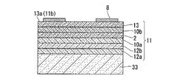
図12は、本発明の第2の実施形態に係る発光ダイオードを説明するための図であり、図12(a)は、第2の実施形態の発光ダイオードの平面図であり、図12(b)は、図12(a)に示す発光ダイオードのA−A‘線方向の概略断面図である。
図12を参照するに、第2の実施形態の発光ダイオード50は、第1の実施形態の発光ダイオード1に設けられた機能性基板5(金属基板)の替わりに、機能性基板5(金属基板)とは異なる材料により構成された機能性基板51を設けると共に、さらに金属層52,53を設け、上部クラッド層10aの上面を覆うようにコンタクト層12bを配置した以外は、第1の実施形態の発光ダイオード1と同様に構成される。
つまり、第2の実施形態の発光ダイオード50と第1の実施形態の発光ダイオード1との大きな相違点は、機能性基板の材料が異なる点である。
(Second Embodiment)
FIG. 12 is a diagram for explaining a light emitting diode according to a second embodiment of the present invention, and FIG. 12A is a plan view of the light emitting diode of the second embodiment, and FIG. ) Is a schematic cross-sectional view of the light-emitting diode shown in FIG.
Referring to FIG. 12, the
That is, the major difference between the
機能性基板51は、金属層52を介して、化合物半導体層11が設けられた反射構造体4(具体的には、反射層15)に接合されている。機能性基板51の材料としては、GaP、Si、Geのいずれかの材料を用いることができる。
このように、GaP、Si、Geのいずれかの材料よりなる機能性基板51を設けることにより、機能性基板51を備えていない発光ダイオードと比較して、発光部3が発光した際の熱を、発光ダイオード50の外部に効率良く放熱することができる。
また、腐食しにくい材料であるSiやGe等を機能性基板51の材料として用いることで、機能性基板51の耐湿性を向上させることができる。
The
In this way, by providing the
Moreover, the moisture resistance of the
金属層52は、反射構造体4を構成する反射層15と機能性基板51の上面51aとの間に設けられている。金属層52は、反射層15と機能性基板51の上面51aとを接合するための層である。金属層52としては、例えば、In層と、Au層と、Ti層とを順次積層した積層膜を用いることができる。
金属層53は、機能性基板51の下面51bに設けられている。金属層53としては、例えば、Au層と、Ti層とを順次積層した積層膜を用いることができる。
The
The
第2の実施形態の発光ダイオードによれば、金属層52を介して、化合物半導体層11が設けられた反射構造体4に接合され、かつGaP、Si、Geのいずれかの材料により構成された機能性基板51を設けることにより、機能性基板51を備えていない発光ダイオードと比較して、発光部3が発光した際の熱を、発光ダイオード50の外部に効率良く放熱することができる。
また、腐食しにくい材料であるSiやGe等を機能性基板51の材料として用いることで、機能性基板51の耐湿性を向上させることができる。
According to the light emitting diode of the second embodiment, the
Moreover, the moisture resistance of the
また、化合物半導体層11の光取り出し面11aとは反対側に位置する化合物半導体層11の面11bに、反射構造体4を設けることにより、化合物半導体層11の光取り出し面11aから発光ダイオード1の外部に放射される光のうち、光取り出し面11aに対して直交する方向(具体的には、正面方向f)における光の強度を強くすることが可能となるので、高輝度及び高効率の発光ダイオード50を実現できる。
Further, the
また、第2の実施形態の発光ダイオード50は、組成式(AlXGa1−X)YIn1−YP(0≦X≦0.1、0.37≦Y≦0.46)よりなる歪発光層31とバリア層32との積層構造とされた発光部3を備えているため、発光部3から放射される光の発光効率及び応答速度を向上できる。
また、歪発光層31の組成を上記範囲に規定することにより、655nm以上の発光波長を有した発光ダイオード1を実現できる。
さらに、発光部3上に、発光部3の光を透過させる歪調整層13を備えることにより、歪調整層13により発光部3からの光が吸収されることがないため、高出力・高効率の発光ダイオード50を実現できる。
Further, the
Further, by defining the composition of the strained
Further, since the
また、上記歪調整層13は、歪発光層31及びバリア層32の格子定数よりも小さい格子定数を有しているため、半導体化合物層11の反りの発生を抑制できる。これにより、歪発光層31の歪量のばらつきが低減されるため、単色性に優れた発光ダイオード50を実現できる。
Further, since the
以下、本発明の効果を、実施例を用いて具体的に説明する。なお、本発明はこれらの実施例に限定されるものではない。 Hereinafter, the effect of the present invention will be specifically described with reference to examples. The present invention is not limited to these examples.
本実施例では、本発明に係る発光ダイオードを作製した例を具体的に説明する。発光ダイオードを作製した後、特性評価のために発光ダイオードチップを基板上に実装した発光ダイオードランプを作製した。 In this example, an example in which a light-emitting diode according to the present invention is manufactured will be specifically described. After the light emitting diode was manufactured, a light emitting diode lamp having a light emitting diode chip mounted on a substrate was prepared for characteristic evaluation.
(実施例1)
実施例1の発光ダイオード(第1の実施形態)は、先ず、Siをドープしたn型のGaAs単結晶からなるGaAs基板(厚さ約0.5μm)上に、化合物半導体層を順次積層してエピタキシャルウェーハを作製した。GaAs基板は、(100)面から(0−1−1)方向に15°傾けた面を成長面とし、キャリア濃度を2×1018cm−3とした。
また、化合物半導体層として、GaAs基板上に、SiをドープしたGaAsからなるn型の緩衝層と、Siをドープした(Al0.7Ga0.3)0.5In0.5Pからなるn型のコンタクト層と、Siをドープした(Al0.7Ga0.3)0.5In0.5Pからなるn型の上部クラッド層と、アンドープのGa0.44In0.56P/(Al0.53Ga0.47)0.5In0.5Pの対からなる歪発光層/バリア層と、Mgをドープした(Al0.7Ga0.3)0.5In0.5Pよりなるp型の下部クラッド層と、(Al0.5Ga0.5)0.5In0.5Pよりなる薄膜の中間層と、Mgドープしたp型GaPよりなる歪調整層と、を順次形成した。
Example 1
In the light emitting diode of the first embodiment (first embodiment), first, compound semiconductor layers are sequentially stacked on a GaAs substrate (thickness: about 0.5 μm) made of n-type GaAs single crystal doped with Si. An epitaxial wafer was produced. In the GaAs substrate, a plane inclined by 15 ° in the (0-1-1) direction from the (100) plane was used as a growth plane, and the carrier concentration was set to 2 × 10 18 cm −3 .
Further, the compound semiconductor layer is composed of an n-type buffer layer made of GaAs doped with Si on a GaAs substrate and (Al 0.7 Ga 0.3 ) 0.5 In 0.5 P doped with Si. an n-type contact layer, an n-type upper cladding layer made of Si-doped (Al 0.7 Ga 0.3 ) 0.5 In 0.5 P, and undoped Ga 0.44 In 0.56 P / (Al 0.53 Ga 0.47 ) 0.5 In 0.5 P pair strained light emitting layer / barrier layer and Mg-doped (Al 0.7 Ga 0.3 ) 0.5 In 0 .5 a lower cladding layer of p-type consisting of P, (Al 0.5 Ga 0.5) 0.5 in 0.5 an intermediate layer of a thin film made of P, strain adjustment layer composed of p-type GaP that Mg-doped Were sequentially formed.
実施例1では、減圧有機金属化学気相堆積装置法(MOCVD装置)を用い、直径76mm、厚さ350μmのGaAs基板に化合物半導体層をエピタキシャル成長させて、エピタキシャルウェーハを形成した。
エピタキシャル成長層を成長させる際、III族構成元素の原料としては、トリメチルアルミニウム((CH3)3Al)、トリメチルガリウム((CH3)3Ga)及びトリメチルインジウム((CH3)3In)を使用した。また、Mgのドーピング原料としては、ビスシクロペンタジエニルマグネシウム(bis−(C5H5)2Mg)を使用した。また、Siのドーピング原料としては、ジシラン(Si2H6)を使用した。
また、V族構成元素の原料としては、ホスフィン(PH3)、アルシン(AsH3)を使用した。また、各層の成長温度としては、p型GaPからなる歪調整層は、750℃で成長させた。その他の各層では700℃で成長させた。
In Example 1, a compound semiconductor layer was epitaxially grown on a GaAs substrate having a diameter of 76 mm and a thickness of 350 μm by using a low pressure metal organic chemical vapor deposition apparatus method (MOCVD apparatus) to form an epitaxial wafer.
When growing an epitaxial growth layer, trimethylaluminum ((CH 3 ) 3 Al), trimethylgallium ((CH 3 ) 3 Ga) and trimethylindium ((CH 3 ) 3 In) are used as the raw material for the group III constituent element did. Further, biscyclopentadienyl magnesium (bis- (C 5 H 5 ) 2 Mg) was used as a Mg doping material. Further, disilane (Si 2 H 6 ) was used as a Si doping material.
Further, phosphine (PH 3 ) and arsine (AsH 3 ) were used as raw materials for the group V constituent elements. Moreover, as a growth temperature of each layer, the strain adjustment layer made of p-type GaP was grown at 750 ° C. The other layers were grown at 700 ° C.
GaAsよりなる緩衝層は、キャリア濃度を約2×1018cm−3、層厚を約0.5μmとした。コンタクト層は、キャリア濃度を約2×1018cm−3、層厚を約3.5μmとした。上部クラッド層は、キャリア濃度を約1×1018cm−3、層厚を約0.5μmとした。
実施例1では、アンドープでGa0.44In0.56Pよりなる23層の歪発光層(単層の厚さが17nm)と、かつ組成が(Al0.53Ga0.47)0.5In0.5Pの22層のバリア層(単層の厚さが19nm)とを交互に積層することで、発光層を形成した。
下部クラッド層は、キャリア濃度を約8×1017cm−3、層厚を約0.5μmとした。中間層は、キャリア濃度を約8×1017cm−3、層厚を約0.05μmとした。GaPからなる歪調整層は、キャリア濃度を約3×1018cm−3、層厚を約9μmとした。
The buffer layer made of GaAs has a carrier concentration of about 2 × 10 18 cm −3 and a layer thickness of about 0.5 μm. The contact layer had a carrier concentration of about 2 × 10 18 cm −3 and a layer thickness of about 3.5 μm. The upper cladding layer had a carrier concentration of about 1 × 10 18 cm −3 and a layer thickness of about 0.5 μm.
In Example 1, 23 strained light emitting layers (single layer thickness: 17 nm) made of undoped Ga 0.44 In 0.56 P and a composition of (Al 0.53 Ga 0.47 ) 0. A light emitting layer was formed by alternately stacking 22 barrier layers (single layer thickness: 19 nm) of 5 In 0.5 P.
The lower cladding layer had a carrier concentration of about 8 × 10 17 cm −3 and a layer thickness of about 0.5 μm. The intermediate layer had a carrier concentration of about 8 × 10 17 cm −3 and a layer thickness of about 0.05 μm. The strain adjusting layer made of GaP had a carrier concentration of about 3 × 10 18 cm −3 and a layer thickness of about 9 μm.
次に、歪調整層を表面から約1μmの深さに至る領域まで研磨して鏡面加工した。この鏡面加工によって、歪調整層の表面の粗さを0.18nmとした。
次いで、歪調整層上に、AuBe層(厚さ100nm)と、Au層(厚さ150nm)とを順次成膜することで、AuBe/Au積層膜を形成し、その後、一般的なフォトリソグラフィー技術及びエッチング技術を利用して、AuBe/Au積層膜をパターニングすることで、第2の電極を形成した。
次いで、歪調整層上に、第2の電極を覆う透明導電膜としてITO膜(厚さ***nm)と、反射層としてAg合金(厚さ500nm)/W(厚さ100nm)/Pt(厚さ200nm)/Au(厚さ500nm)/AuGe(厚さ1000nm)積層膜とを順次成膜することで、反射構造体を形成する。
次に、第1の実施形態で説明した方法を用いて、Cu(30μm)/Mo(25μm)/Cu(30μm)の3層構造(厚さ85μm)からなる機能性基板(金属基板(熱伝導率250W/mK))を製造した。
実施例1の機能性基板の熱膨張係数は、6.1ppm/Kであり、熱伝導率は250W/m・Kであった。また、機能性基板の直径は76mmで、厚さは250μmであった。
Next, the strain adjusting layer was polished to a region extending from the surface to a depth of about 1 μm and mirror-finished. By this mirror finishing, the surface roughness of the strain adjustment layer was set to 0.18 nm.
Next, an AuBe layer (thickness: 100 nm) and an Au layer (thickness: 150 nm) are sequentially formed on the strain adjustment layer, thereby forming an AuBe / Au laminated film, and then a general photolithography technique. The second electrode was formed by patterning the AuBe / Au laminated film using the etching technique.
Next, on the strain adjustment layer, an ITO film (thickness *** nm) as a transparent conductive film covering the second electrode, and an Ag alloy (thickness 500 nm) / W (thickness 100 nm) / Pt (reflection layer) A reflective structure is formed by sequentially forming a stacked film of 200 nm in thickness) / Au (thickness 500 nm) / AuGe (thickness 1000 nm).
Next, using the method described in the first embodiment, a functional substrate (metal substrate (heat conduction) having a three-layer structure (thickness 85 μm) of Cu (30 μm) / Mo (25 μm) / Cu (30 μm) is used. 250 W / mK)).
The functional substrate of Example 1 had a thermal expansion coefficient of 6.1 ppm / K and a thermal conductivity of 250 W / m · K. The functional substrate had a diameter of 76 mm and a thickness of 250 μm.
次に、減圧装置内を3×10⁻⁵Paまで排気した後、GaAs基板と機能性基板とを400℃に加熱した状態で、100g/cm2の加重を印加して反射構造体と機能性基板と接合して、接合構造体を形成した。 Next, after evacuating the inside of the decompression device to 3 × 10 −5 Pa, a weight of 100 g / cm 2 is applied in a state where the GaAs substrate and the functional substrate are heated to 400 ° C. The bonded structure was formed by bonding to the substrate.
次に、上記接合構造体から、GaAs基板及びGaAs緩衝層をアンモニア系エッチャントにより選択的に除去した。次に、真空蒸着法により、コンタクト層の表面に、厚さが0.5μmのAu−Ge−Ni合金膜と、厚さが0.2μmのPt膜と、厚さが1μmのAu膜とを順次成膜した。
その後、一般的なフォトリソグラフィー技術及びエッチング技術を利用して、上記Au−Ge−Ni合金膜、Pt膜、及びAu膜をパターニングすることで、第1の電極であるn型オーミック電極を形成した。その後、第1の電極の形状に対応するように、周知の手法により、コンタクト層をパターニングした。
次に、GaAs基板を除去した面である光取り出し面の表面に粗面化処理を施した。
Next, the GaAs substrate and the GaAs buffer layer were selectively removed from the bonded structure with an ammonia-based etchant. Next, an Au—Ge—Ni alloy film having a thickness of 0.5 μm, a Pt film having a thickness of 0.2 μm, and an Au film having a thickness of 1 μm are formed on the surface of the contact layer by vacuum deposition. Films were sequentially formed.
Thereafter, the Au-Ge-Ni alloy film, the Pt film, and the Au film were patterned by using a general photolithography technique and an etching technique, thereby forming an n-type ohmic electrode as the first electrode. . Thereafter, the contact layer was patterned by a known method so as to correspond to the shape of the first electrode.
Next, the surface of the light extraction surface, which is the surface from which the GaAs substrate was removed, was roughened.
その後、450℃で10分間熱処理を行って合金化し、低抵抗の第1及び第2の電極(n型及びp型オーミック電極)を形成した。
Later, alloyed by heat treatment for 10 minutes at 450 ° C., to form the first and second electrodes of the low-resistance (n-type and p-type ohmic electrode).
次に、ダイシングソーを用いて、第1及び第2の電極が形成された接合構造体を切断して、チップ化した。これにより、実施例1の発光ダイオードを作製した。 Next, using a dicing saw, the joined structure on which the first and second electrodes were formed was cut into chips. Thereby, the light emitting diode of Example 1 was produced.
上記方法により作製した実施例1の発光ダイオードチップを、マウント基板上に実装した発光ダイオードランプを100個組み立てた。この発光ダイオードランプは、マウントは、共晶ダイボンダーで、加熱接続され支持(マウント)し、発光ダイオードのn型オーミック電極とマウント基板の表面に設けたn電極端子とを金線でワイヤボンディングし、p型オーミック電極とp電極端子とを金線でワイヤボンディングした後、一般的なエポキシ樹脂で封止して作製した。 100 light emitting diode lamps each having the light emitting diode chip of Example 1 manufactured by the above method mounted on a mount substrate were assembled. In this light emitting diode lamp, the mount is heated and connected (mounted) with a eutectic die bonder, and the n-type ohmic electrode of the light emitting diode and the n electrode terminal provided on the surface of the mounting substrate are wire-bonded with a gold wire, The p-type ohmic electrode and the p-electrode terminal were wire-bonded with a gold wire and then sealed with a general epoxy resin.
実施例1の発光ダイオードの構成要素の一部を表1に示し、実施例1の発光ダイオードを実装した発光ダイオードランプの特性を評価した結果を表2に示す。
表2に示すように、n型及びp型オーミック電極間に電流を流したところ、ピーク発光波長661.2nm(655nm以上の値)とする赤色光が出射された。
また、順方向に20ミリアンペア(mA)の電流を通流した際の順方向電圧(Vf)は、化合物半導体層を構成する歪調整層と機能性基板との接合界面での抵抗の低さ及び各オーミック電極の良好なオーミック特性を反映し、2.1ボルト(V)となった。
順方向電流を20mAとした際の発光出力は、4.1mW(3mW以上)であり、良好な結果が得られた。
Some of the components of the light-emitting diode of Example 1 are shown in Table 1, and the results of evaluating the characteristics of the light-emitting diode lamp mounted with the light-emitting diode of Example 1 are shown in Table 2.
As shown in Table 2, when a current was passed between the n-type and p-type ohmic electrodes, red light having a peak emission wavelength of 661.2 nm (value of 655 nm or more) was emitted.
In addition, the forward voltage (Vf) when a current of 20 milliamperes (mA) flows in the forward direction is low in resistance at the bonding interface between the strain adjustment layer and the functional substrate constituting the compound semiconductor layer, and Reflecting the good ohmic characteristics of each ohmic electrode, it was 2.1 volts (V).
The light emission output when the forward current was 20 mA was 4.1 mW (3 mW or more), and good results were obtained.
組み立てたすべての発光ダイオードにおけるピーク発光波長のバラツキ(最大−最小)は、2.1nmであり、良好な結果が得られた。なお、ピーク発光波長のバラツキ(最大−最小)は、3nm以下であればよい。
また、発光の立ち上がりの応答速度(Tr)は、72nsであり、100ns以下の良好な結果が得られた。また、表面欠陥の検査では、表面欠陥は見られなかった。
The variation (maximum-minimum) of the peak emission wavelength in all the assembled light-emitting diodes was 2.1 nm, and good results were obtained. In addition, the variation (maximum-minimum) of the peak emission wavelength may be 3 nm or less.
Moreover, the response speed (Tr) of the rise of light emission was 72 ns, and good results of 100 ns or less were obtained. Also, no surface defects were found in the surface defect inspection.
また、光取り出し面に対して90°の角度を成す方向に放射される放射照度Eを、光取り出し面に対して45°の角度を成す方向に放射される放射照度Fで割った放射照度の比(=E/F)は、1.43(1.0よりも大きい値)であり、光取り出し面に対して90°の角度を成す方向に放射される放射照度Eが強くなっていることが確認できた。
また、実施例1の発光ダイオードが発光した際、機能性基板の放熱効果により、温度上昇に起因する発光効率の低下は見られなかった。
Further, the irradiance obtained by dividing the irradiance E radiated in a direction forming an angle of 90 ° with respect to the light extraction surface by the irradiance F radiated in a direction forming an angle of 45 ° with the light extraction surface. The ratio (= E / F) is 1.43 (value greater than 1.0), and the irradiance E radiated in a direction forming an angle of 90 ° with respect to the light extraction surface is strong. Was confirmed.
Further, when the light emitting diode of Example 1 emitted light, no decrease in light emission efficiency due to temperature increase was observed due to the heat dissipation effect of the functional substrate.
図13は、本発明の第1実施例の発光ダイオードランプの発光スペクトルを示す図である。
図13に示すように、実施例1の発光ダイオードランプの発光スペクトルは、半値幅が18nmであり、波長700nmにおける発光強度がほぼ0であった。
FIG. 13 is a diagram showing an emission spectrum of the light-emitting diode lamp of the first embodiment of the present invention.
As shown in FIG. 13, the emission spectrum of the light-emitting diode lamp of Example 1 had a half width of 18 nm and the emission intensity at a wavelength of 700 nm was almost zero.
上記結果から、実施例1の発光ダイオード及び発光ダイオードランプによれば、655nm以上の発光波長を有した光を発光する発光層を形成でき、かつ100ns以下の応答速度(この場合、72ns)を実現できることが確認できた。
また、実施例1の発光ダイオード及び発光ダイオードランプによれば、放射照度の比(=E/F)が1.43(1.0よりも大きい値)であるので、高輝度及び高効率の発光ダイオードが実現できることが確認できた。
さらに、機能性基板の放熱効果により、放熱特性に優れた発光ダイオードを実現できることが確認できた。
From the above results, according to the light-emitting diode and the light-emitting diode lamp of Example 1, a light-emitting layer that emits light having an emission wavelength of 655 nm or more can be formed, and a response speed of 100 ns or less (72 ns in this case) is realized. I was able to confirm that it was possible.
Further, according to the light emitting diode and the light emitting diode lamp of Example 1, the irradiance ratio (= E / F) is 1.43 (a value larger than 1.0), so that the light emission with high luminance and high efficiency is achieved. It was confirmed that a diode could be realized.
Furthermore, it was confirmed that a light emitting diode having excellent heat dissipation characteristics can be realized by the heat dissipation effect of the functional substrate.
(実施例2)
実施例2の発光ダイオード(第2の実施形態)は、実施例1の発光ダイオードに設けられた発光層の替わりに、アンドープのGa0.42In0.58Pよりなる21層の歪発光層(単層の厚さ10nm)と、組成が(Al0.53Ga0.47)0.5In0.5Pの20層のバリア層(単層の厚さが30nm)とを交互に積層して発光層を形成すると共に、機能性基板として厚さが150μmのGaP層(熱伝導率110W/mK)を用いた以外は、実施例1の発光ダイオードと同様に製造した。
(Example 2)
The light-emitting diode of Example 2 (second embodiment) is a 21-layer strained light-emitting layer made of undoped Ga 0.42 In 0.58 P, instead of the light-emitting layer provided in the light-emitting diode of Example 1. (Single layer thickness 10 nm) and 20 barrier layers (
実施例2の発光ダイオードの構成要素の一部を表1に示し、実施例2の発光ダイオードを実装した発光ダイオードランプの特性を評価した結果を表2に示す。
表2に示すように、n型及びp型オーミック電極間に電流を流したところ、ピーク発光波長660.7nm(655nm以上の値)とする赤色光が出射された。
また、順方向に20ミリアンペア(mA)の電流を通流した際の順方向電圧(Vf)は、化合物半導体層を構成する歪調整層と機能性基板との接合界面での抵抗の低さ及び各オーミック電極の良好なオーミック特性を反映し、2.1ボルト(V)となった。
また、順方向電流を20mAとした際の発光出力は、3.6mW(3mW以上)であり、良好な結果が得られた。)。
Some of the components of the light-emitting diode of Example 2 are shown in Table 1, and the results of evaluating the characteristics of the light-emitting diode lamp mounted with the light-emitting diode of Example 2 are shown in Table 2.
As shown in Table 2, when a current was passed between the n-type and p-type ohmic electrodes, red light having a peak emission wavelength of 660.7 nm (a value of 655 nm or more) was emitted.
In addition, the forward voltage (Vf) when a current of 20 milliamperes (mA) flows in the forward direction is low in resistance at the bonding interface between the strain adjustment layer and the functional substrate constituting the compound semiconductor layer, and Reflecting the good ohmic characteristics of each ohmic electrode, it was 2.1 volts (V).
The light emission output when the forward current was 20 mA was 3.6 mW (3 mW or more), and a good result was obtained. ).
組み立てたすべての発光ダイオードにおけるピーク発光波長のバラツキ(最大−最小)は、2.3nmであり、良好な結果が得られた。また、発光の立ち上がりの応答速度(Tr)は、70nsであり、100ns以下の良好な結果が得られた。また、表面欠陥の検査では、表面欠陥は見られなかった。 The variation of the peak emission wavelength (maximum-minimum) in all the assembled light emitting diodes was 2.3 nm, and good results were obtained. The response speed (Tr) of the rise of light emission was 70 ns, and good results of 100 ns or less were obtained. Also, no surface defects were found in the surface defect inspection.
また、光取り出し面に対して90°の角度を成す方向に放射される放射照度Eを、光取り出し面に対して45°の角度を成す方向に放射される放射照度Fで割った放射照度の比(=E/F)は、1.17(1.0よりも大きい値)であり、光取り出し面に対して90°の角度を成す方向に放射される放射照度Eが強くなっていることが確認できた。
また、実施例2の発光ダイオードが発光した際、機能性基板の放熱効果により、温度上昇に起因する発光効率の低下は見られなかった。
Further, the irradiance obtained by dividing the irradiance E radiated in a direction forming an angle of 90 ° with respect to the light extraction surface by the irradiance F radiated in a direction forming an angle of 45 ° with respect to the light extraction surface. The ratio (= E / F) is 1.17 (a value larger than 1.0), and the irradiance E radiated in a direction forming an angle of 90 ° with respect to the light extraction surface is strong. Was confirmed.
In addition, when the light emitting diode of Example 2 emitted light, no decrease in light emission efficiency due to temperature increase was observed due to the heat dissipation effect of the functional substrate.
上記結果から、実施例2の発光ダイオード及び発光ダイオードランプによれば、655nm以上の発光波長を有した光を発光する発光層を構成でき、かつ100ns以下の応答速度(この場合、70ns)を実現できることが確認できた。
また、実施例2の発光ダイオード及び発光ダイオードランプによれば、放射照度の比(=E/F)が1.17(1.0よりも大きい値)であるので、高輝度及び高効率の発光ダイオードが実現できることが確認できた。
さらに、機能性基板の放熱効果により、放熱特性に優れた発光ダイオードを実現できることが確認できた。
From the above results, according to the light-emitting diode and the light-emitting diode lamp of Example 2, a light-emitting layer that emits light having an emission wavelength of 655 nm or more can be formed, and a response speed of 100 ns or less (in this case, 70 ns) can be realized. I was able to confirm that it was possible.
Further, according to the light emitting diode and the light emitting diode lamp of Example 2, the ratio of irradiance (= E / F) is 1.17 (a value larger than 1.0), so that light emission with high luminance and high efficiency is achieved. It was confirmed that a diode could be realized.
Furthermore, it was confirmed that a light emitting diode having excellent heat dissipation characteristics can be realized by the heat dissipation effect of the functional substrate.
(実施例3)
実施例3の発光ダイオード(第2の実施形態)は、実施例2の発光ダイオードに設けられた歪発光層の替わりに、アンドープのGa0.41In0.59Pよりなる21層の歪発光層(単層の厚さが15nm)を形成すると共に、機能性基板として厚さが100μmのGe層(熱伝導率60W/mK)を用いた以外は、実施例2の発光ダイオードと同様に製造した。
(Example 3)
The light-emitting diode of Example 3 (second embodiment) is a 21-layer strained light emission made of undoped Ga 0.41 In 0.59 P instead of the strained light-emitting layer provided in the light-emitting diode of Example 2. Manufactured in the same manner as the light-emitting diode of Example 2, except that a layer (single layer thickness of 15 nm) was formed and a Ge layer (thermal conductivity 60 W / mK) having a thickness of 100 μm was used as a functional substrate. did.
実施例3の発光ダイオードの構成要素の一部を表1に示し、実施例3の発光ダイオードを実装した発光ダイオードランプの特性を評価した結果を表2に示す。
表2に示すように、n型及びp型オーミック電極間に電流を流したところ、ピーク発光波長668.5nm(655nm以上の値)とする赤色光が出射された。
また、順方向に20ミリアンペア(mA)の電流を通流した際の順方向電圧(Vf)は、化合物半導体層を構成する歪調整層と機能性基板との接合界面での抵抗の低さ及び各オーミック電極の良好なオーミック特性を反映し、2.1ボルト(V)となった。
また、順方向電流を20mAとした際の発光出力は、3.7mW(3mW以上)であり、良好な結果が得られた。
Some of the components of the light emitting diode of Example 3 are shown in Table 1, and the results of evaluating the characteristics of the light emitting diode lamp mounted with the light emitting diode of Example 3 are shown in Table 2.
As shown in Table 2, when a current was passed between the n-type and p-type ohmic electrodes, red light having a peak emission wavelength of 668.5 nm (a value of 655 nm or more) was emitted.
In addition, the forward voltage (Vf) when a current of 20 milliamperes (mA) flows in the forward direction is low in resistance at the bonding interface between the strain adjustment layer and the functional substrate constituting the compound semiconductor layer, and Reflecting the good ohmic characteristics of each ohmic electrode, it was 2.1 volts (V).
The light emission output when the forward current was 20 mA was 3.7 mW (3 mW or more), and a good result was obtained.
組み立てたすべての発光ダイオードにおけるピーク発光波長のバラツキ(最大−最小)は、2.5nmであり、良好な結果が得られた。また、発光の立ち上がりの応答速度(Tr)は、73nsであり、100ns以下の良好な結果が得られた。また、表面欠陥の検査では、表面欠陥は見られなかった。 The variation of the peak emission wavelength (maximum-minimum) in all the assembled light emitting diodes was 2.5 nm, and good results were obtained. Further, the response speed (Tr) of the rise of light emission was 73 ns, and a good result of 100 ns or less was obtained. Also, no surface defects were found in the surface defect inspection.
また、光取り出し面に対して90°の角度を成す方向に放射される放射照度Eを、光取り出し面に対して45°の角度を成す方向に放射される放射照度Fで割った放射照度の比(=E/F)は、1.22(1.0よりも大きい値)であり、光取り出し面に対して90°の角度を成す方向に放射される放射照度Eが強くなっていることが確認できた。
また、実施例3の発光ダイオードが発光した際、機能性基板の放熱効果により、温度上昇に起因する発光効率の低下は見られなかった。
Further, the irradiance obtained by dividing the irradiance E radiated in a direction forming an angle of 90 ° with respect to the light extraction surface by the irradiance F radiated in a direction forming an angle of 45 ° with respect to the light extraction surface. The ratio (= E / F) is 1.22 (value greater than 1.0), and the irradiance E radiated in a direction forming an angle of 90 ° with respect to the light extraction surface is strong. Was confirmed.
Further, when the light emitting diode of Example 3 emitted light, no reduction in light emission efficiency due to temperature increase was observed due to the heat dissipation effect of the functional substrate.
上記結果から、実施例3の発光ダイオード及び発光ダイオードランプによれば、655nm以上の発光波長を有した光を発光する発光層を構成でき、かつ100ns以下の応答速度(この場合、73ns)を実現できることが確認できた。
また、実施例3の発光ダイオード及び発光ダイオードランプによれば、放射照度の比(=E/F)が1.22(1.0よりも大きい値)であるので、高輝度及び高効率の発光ダイオードが実現できることが確認できた。
さらに、機能性基板の放熱効果により、放熱特性に優れた発光ダイオードを実現できることが確認できた。
From the above results, according to the light-emitting diode and light-emitting diode lamp of Example 3, a light-emitting layer that emits light having an emission wavelength of 655 nm or more can be configured, and a response speed of 100 ns or less (in this case, 73 ns) can be realized. I was able to confirm that it was possible.
Further, according to the light emitting diode and the light emitting diode lamp of Example 3, since the irradiance ratio (= E / F) is 1.22 (a value larger than 1.0), light emission with high luminance and high efficiency is achieved. It was confirmed that a diode could be realized.
Furthermore, it was confirmed that a light emitting diode having excellent heat dissipation characteristics can be realized by the heat dissipation effect of the functional substrate.
(実施例4)
実施例4の発光ダイオード(第2の実施形態)は、実施例2の発光ダイオードに設けられた歪発光層の替わりに、アンドープのGa0.45In0.55Pよりなる21層の歪発光層(単層の厚さが25nm)を形成すると共に、機能性基板として厚さが100μmのSi層(熱伝導率126W/mK)を用いた以外は、実施例2の発光ダイオードと同様に製造した。
Example 4
The light-emitting diode of Example 4 (second embodiment) is a 21-layer strained light emission made of undoped Ga 0.45 In 0.55 P, instead of the strained light-emitting layer provided in the light-emitting diode of Example 2. Manufactured in the same manner as the light-emitting diode of Example 2, except that a layer (single layer thickness of 25 nm) was formed and a Si layer (thermal conductivity 126 W / mK) having a thickness of 100 μm was used as the functional substrate. did.
実施例4の発光ダイオードの構成要素の一部を表1に示し、実施例4の発光ダイオードを実装した発光ダイオードランプの特性を評価した結果を表2に示す。
表2に示すように、n型及びp型オーミック電極間に電流を流したところ、ピーク発光波長657.0nm(655nm以上の値)とする赤色光が出射された。
また、順方向に20ミリアンペア(mA)の電流を通流した際の順方向電圧(Vf)は、化合物半導体層を構成する歪調整層と機能性基板との接合界面での抵抗の低さ及び各オーミック電極の良好なオーミック特性を反映し、2.1ボルト(V)となった。
順方向電流を20mAとした際の発光出力は、4.0mW(3mW以上)であり、良好な結果が得られた。
Some of the components of the light-emitting diode of Example 4 are shown in Table 1, and the results of evaluating the characteristics of the light-emitting diode lamp mounted with the light-emitting diode of Example 4 are shown in Table 2.
As shown in Table 2, when a current was passed between the n-type and p-type ohmic electrodes, red light having a peak emission wavelength of 657.0 nm (a value of 655 nm or more) was emitted.
In addition, the forward voltage (Vf) when a current of 20 milliamperes (mA) flows in the forward direction is low in resistance at the bonding interface between the strain adjustment layer and the functional substrate constituting the compound semiconductor layer, and Reflecting the good ohmic characteristics of each ohmic electrode, it was 2.1 volts (V).
The light emission output when the forward current was 20 mA was 4.0 mW (3 mW or more), and good results were obtained.
組み立てたすべての発光ダイオードにおけるピーク発光波長のバラツキ(最大−最小)は、2.1nmであり、良好な結果が得られた。また、発光の立ち上がりの応答速度(Tr)は、64nsであり、100ns以下の良好な結果が得られた。また、表面欠陥の検査では、表面欠陥は見られなかった。 The variation (maximum-minimum) of the peak emission wavelength in all the assembled light-emitting diodes was 2.1 nm, and good results were obtained. In addition, the response speed (Tr) of the rise of light emission was 64 ns, and good results of 100 ns or less were obtained. Also, no surface defects were found in the surface defect inspection.
また、光取り出し面に対して90°の角度を成す方向に放射される放射照度Eを、光取り出し面に対して45°の角度を成す方向に放射される放射照度Fで割った放射照度(=E/F)は、1.33(1.0よりも大きい値)であり、光取り出し面に対して90°の角度を成す方向に放射される放射照度Eが強くなっていることが確認できた。
また、実施例4の発光ダイオードが発光した際、機能性基板の放熱効果により、温度上昇に起因する発光効率の低下は見られなかった。
Also, the irradiance (divided by the irradiance F emitted in the direction forming an angle of 45 ° with respect to the light extraction surface by the irradiance E emitted in the direction forming an angle of 90 ° with the light extraction surface ( = E / F) is 1.33 (a value greater than 1.0), and it is confirmed that the irradiance E radiated in a direction forming an angle of 90 ° with respect to the light extraction surface is strong. did it.
Further, when the light emitting diode of Example 4 emitted light, no reduction in light emission efficiency due to temperature increase was observed due to the heat dissipation effect of the functional substrate.
上記結果から、実施例4の発光ダイオード及び発光ダイオードランプによれば、655nm以上の発光波長を有した光を発光する発光層を構成でき、かつ100ns以下の応答速度(この場合、64ns)を実現できることが確認できた。
また、実施例4の発光ダイオード及び発光ダイオードランプによれば、放射照度の比(=E/F)が1.33(1.0よりも大きい値)であるので、高輝度及び高効率の発光ダイオードが実現できることが確認できた。
さらに、機能性基板の放熱効果により、放熱特性に優れた発光ダイオードを実現できることが確認できた。
From the above results, according to the light-emitting diode and the light-emitting diode lamp of Example 4, a light-emitting layer that emits light having an emission wavelength of 655 nm or more can be configured, and a response speed of 100 ns or less (in this case, 64 ns) can be realized. I was able to confirm that it was possible.
Further, according to the light emitting diode and the light emitting diode lamp of Example 4, since the irradiance ratio (= E / F) is 1.33 (a value larger than 1.0), light emission with high luminance and high efficiency is achieved. It was confirmed that a diode could be realized.
Furthermore, it was confirmed that a light emitting diode having excellent heat dissipation characteristics can be realized by the heat dissipation effect of the functional substrate.
(実施例5)
実施例5の発光ダイオード(第1の実施形態)は、実施例2の発光ダイオードに設けられた歪発光層の組成をGa0.39In0.61Pに変更すると共に、Cu(30μm)/Mo(25μm)/Cu(30μm)の3層構造(厚さ85μm)からなる機能性基板(金属基板(熱伝導率250W/mK))を用いた以外は、実施例2の発光ダイオードと同様に製造した。
(Example 5)
In the light-emitting diode of Example 5 (first embodiment), the composition of the strained light-emitting layer provided in the light-emitting diode of Example 2 was changed to Ga 0.39 In 0.61 P and Cu (30 μm) / Similar to the light-emitting diode of Example 2, except that a functional substrate (metal substrate (thermal conductivity 250 W / mK)) having a three-layer structure (thickness 85 μm) of Mo (25 μm) / Cu (30 μm) was used. Manufactured.
実施例5の発光ダイオードの構成要素の一部を表1に示し、実施例5の発光ダイオードを実装した発光ダイオードランプの特性を評価した結果を表2に示す。
表2に示すように、n型及びp型オーミック電極間に電流を流したところ、ピーク発光波長669.8nm(655nm以上の値)とする赤色光が出射された。
また、順方向に20ミリアンペア(mA)の電流を通流した際の順方向電圧(Vf)は、化合物半導体層を構成する歪調整層と機能性基板との接合界面での抵抗の低さ及び各オーミック電極の良好なオーミック特性を反映し、2.1ボルト(V)となった。
順方向電流を20mAとした際の発光出力は、3.9mW(3mW以上)であり、良好な結果が得られた。)。
Some of the components of the light-emitting diode of Example 5 are shown in Table 1, and the results of evaluating the characteristics of the light-emitting diode lamp mounted with the light-emitting diode of Example 5 are shown in Table 2.
As shown in Table 2, when a current was passed between the n-type and p-type ohmic electrodes, red light having a peak emission wavelength of 669.8 nm (value of 655 nm or more) was emitted.
In addition, the forward voltage (Vf) when a current of 20 milliamperes (mA) flows in the forward direction is low in resistance at the bonding interface between the strain adjustment layer and the functional substrate constituting the compound semiconductor layer, and Reflecting the good ohmic characteristics of each ohmic electrode, it was 2.1 volts (V).
The light emission output when the forward current was 20 mA was 3.9 mW (3 mW or more), and good results were obtained. ).
組み立てたすべての発光ダイオードにおけるピーク発光波長のバラツキ(最大−最小)は、2.9nmであり、良好な結果が得られた。また、発光の立ち上がりの応答速度(Tr)は、63nsであり、100ns以下の良好な結果が得られた。また、表面欠陥の検査では、表面欠陥は見られなかった。 The variation of the peak emission wavelength (maximum-minimum) in all the assembled light emitting diodes was 2.9 nm, and good results were obtained. Further, the response speed (Tr) of the rise of light emission was 63 ns, and good results of 100 ns or less were obtained. Also, no surface defects were found in the surface defect inspection.
また、光取り出し面に対して90°の角度を成す方向に放射される放射照度Eを、光取り出し面に対して45°の角度を成す方向に放射される放射照度Fで割った放射照度の比(=E/F)は、1.41(1.0よりも大きい値)であり、光取り出し面に対して90°の角度を成す方向に放射される放射照度Eが強くなっていることが確認できた。
また、実施例5の発光ダイオードが発光した際、機能性基板の放熱効果により、温度上昇に起因する発光効率の低下は見られなかった。
Further, the irradiance obtained by dividing the irradiance E radiated in a direction forming an angle of 90 ° with respect to the light extraction surface by the irradiance F radiated in a direction forming an angle of 45 ° with respect to the light extraction surface. The ratio (= E / F) is 1.41 (a value greater than 1.0), and the irradiance E radiated in a direction forming an angle of 90 ° with respect to the light extraction surface is strong. Was confirmed.
Further, when the light emitting diode of Example 5 emitted light, no decrease in light emission efficiency due to temperature increase was observed due to the heat dissipation effect of the functional substrate.
上記結果から、実施例5の発光ダイオード及び発光ダイオードランプによれば、655nm以上の発光波長を有した光を発光する発光層を構成でき、かつ100ns以下の応答速度(この場合、63ns)を実現できることが確認できた。
また、実施例5の発光ダイオード及び発光ダイオードランプによれば、放射照度の比(=E/F)が1.41(1.0よりも大きい値)であるので、高輝度及び高効率の発光ダイオードが実現できることが確認できた。
さらに、機能性基板の放熱効果により、放熱特性に優れた発光ダイオードを実現できることが確認できた。
From the above results, according to the light-emitting diode and the light-emitting diode lamp of Example 5, a light-emitting layer that emits light having an emission wavelength of 655 nm or more can be configured, and a response speed of 100 ns or less (in this case, 63 ns) can be realized. I was able to confirm that it was possible.
Further, according to the light-emitting diode and the light-emitting diode lamp of Example 5, the ratio of irradiance (= E / F) is 1.41 (a value greater than 1.0), so that light emission with high luminance and high efficiency is achieved. It was confirmed that a diode could be realized.
Furthermore, it was confirmed that a light emitting diode having excellent heat dissipation characteristics can be realized by the heat dissipation effect of the functional substrate.
(実施例6)
実施例6の発光ダイオード(第1の実施形態)は、実施例5の発光ダイオードに設けられた歪発光層の組成をGa0.38In0.62Pに変更した以外は、実施例5の発光ダイオードと同様に製造した。
(Example 6)
The light emitting diode of Example 6 (first embodiment) is the same as that of Example 5 except that the composition of the strained light emitting layer provided in the light emitting diode of Example 5 is changed to Ga 0.38 In 0.62 P. Manufactured in the same manner as the light emitting diode.
実施例6の発光ダイオードの構成要素の一部を表1に示し、実施例6の発光ダイオードを実装した発光ダイオードランプの特性を評価した結果を表2に示す。
表2に示すように、n型及びp型オーミック電極間に電流を流したところ、ピーク発光波長675.1nm(655nm以上の値)とする赤色光が出射された。
また、順方向に20ミリアンペア(mA)の電流を通流した際の順方向電圧(Vf)は、化合物半導体層を構成する歪調整層と機能性基板との接合界面での抵抗の低さ及び各オーミック電極の良好なオーミック特性を反映し、2.1ボルト(V)となった。
順方向電流を20mAとした際の発光出力は、3.6mW(3mW以上)であり、良好な結果が得られた。)。
Some of the components of the light-emitting diode of Example 6 are shown in Table 1, and the results of evaluating the characteristics of the light-emitting diode lamp mounted with the light-emitting diode of Example 6 are shown in Table 2.
As shown in Table 2, when a current was passed between the n-type and p-type ohmic electrodes, red light having a peak emission wavelength of 675.1 nm (a value of 655 nm or more) was emitted.
In addition, the forward voltage (Vf) when a current of 20 milliamperes (mA) flows in the forward direction is low in resistance at the bonding interface between the strain adjustment layer and the functional substrate constituting the compound semiconductor layer, and Reflecting the good ohmic characteristics of each ohmic electrode, it was 2.1 volts (V).
The light emission output when the forward current was 20 mA was 3.6 mW (3 mW or more), and good results were obtained. ).
組み立てたすべての発光ダイオードにおけるピーク発光波長のバラツキ(最大−最小)は、2.9nmであり、良好な結果が得られた。また、発光の立ち上がりの応答速度(Tr)は、65nsであり、100ns以下の良好な結果が得られた。また、表面欠陥の検査では、表面欠陥は見られなかった。 The variation of the peak emission wavelength (maximum-minimum) in all the assembled light emitting diodes was 2.9 nm, and good results were obtained. Further, the response speed (Tr) of the rise of light emission was 65 ns, and good results of 100 ns or less were obtained. Also, no surface defects were found in the surface defect inspection.
また、光取り出し面に対して90°の角度を成す方向に放射される放射照度Eを、光取り出し面に対して45°の角度を成す方向に放射される放射照度Fで割った放射照度の比(=E/F)は、1.36(1.0よりも大きい値)であり、光取り出し面に対して90°の角度を成す方向に放射される放射照度Eが強くなっていることが確認できた。
また、実施例6の発光ダイオードが発光した際、機能性基板の放熱効果により、温度上昇に起因する発光効率の低下は見られなかった。
Further, the irradiance obtained by dividing the irradiance E radiated in a direction forming an angle of 90 ° with respect to the light extraction surface by the irradiance F radiated in a direction forming an angle of 45 ° with respect to the light extraction surface. The ratio (= E / F) is 1.36 (value greater than 1.0), and the irradiance E radiated in a direction forming an angle of 90 ° with respect to the light extraction surface is strong. Was confirmed.
Further, when the light emitting diode of Example 6 emitted light, no decrease in light emission efficiency due to temperature increase was observed due to the heat dissipation effect of the functional substrate.
上記結果から、実施例6の発光ダイオード及び発光ダイオードランプによれば、655nm以上の発光波長を有した光を発光する発光層を構成でき、かつ100ns以下の応答速度(この場合、65ns)を実現できることが確認できた。
また、実施例6の発光ダイオード及び発光ダイオードランプによれば、放射照度の比(=E/F)が1.36(1.0よりも大きい値)であるので、高輝度及び高効率の発光ダイオードが実現できることが確認できた。
さらに、機能性基板の放熱効果により、放熱特性に優れた発光ダイオードを実現できることが確認できた。
From the above results, according to the light-emitting diode and the light-emitting diode lamp of Example 6, a light-emitting layer that emits light having an emission wavelength of 655 nm or more can be configured, and a response speed of 100 ns or less (in this case, 65 ns) can be realized. I was able to confirm that it was possible.
Further, according to the light emitting diode and the light emitting diode lamp of Example 6, since the ratio of irradiance (= E / F) is 1.36 (value larger than 1.0), light emission with high luminance and high efficiency is achieved. It was confirmed that a diode could be realized.
Furthermore, it was confirmed that a light emitting diode having excellent heat dissipation characteristics can be realized by the heat dissipation effect of the functional substrate.
(参考例1)
参考例1の発光ダイオードは、実施例2の発光ダイオードの構成から反射構構造体を除去すると共に、実施例2の発光ダイオードに設けられた歪発光層の替わりに、Ga0.38In0.62Pよりなる21層の歪発光層(単層の厚さ5nm)を形成した以外は、第2の実施例の発光ダイオードと同様に製造した。つまり、参考例1の発光ダイオードは、反射構造体を有していない。
(Reference Example 1)
The light emitting diode of Reference Example 1 removes the reflective structure from the configuration of the light emitting diode of Example 2, and replaces the strained light emitting layer provided in the light emitting diode of Example 2 with Ga 0.38 In 0. It was manufactured in the same manner as the light-emitting diode of the second example except that 21 strained light-emitting layers (single layer thickness: 5 nm) made of 62 P were formed. That is, the light emitting diode of Reference Example 1 does not have a reflective structure.
参考例1の発光ダイオードの構成要素の一部を表1に示し、参考例1の発光ダイオードを実装した発光ダイオードランプの特性を評価した結果を表2に示す。
表2に示すように、n型及びp型オーミック電極間に電流を流したところ、ピーク発光波長651.5nm(655nm以下)とする赤色光が出射された。つまり、目標とするピーク発光波長である655nm以上を満たすことができなかった。
また、順方向に20ミリアンペア(mA)の電流を通流した際の順方向電圧(Vf)は、化合物半導体層を構成する歪調整層と機能性基板との接合界面での抵抗の低さ及び各オーミック電極の良好なオーミック特性を反映し、2.0ボルト(V)となった。
また、順方向電流を20mAとした際の発光出力は、3.1mW(3mW以上)であり、良好な結果が得られた。)。
Some of the components of the light emitting diode of Reference Example 1 are shown in Table 1, and the results of evaluating the characteristics of the light emitting diode lamp mounted with the light emitting diode of Reference Example 1 are shown in Table 2.
As shown in Table 2, when a current was passed between the n-type and p-type ohmic electrodes, red light having a peak emission wavelength of 651.5 nm (655 nm or less) was emitted. That is, the target peak emission wavelength of 655 nm or more could not be satisfied.
Further, the forward voltage (Vf) when a current of 20 milliamperes (mA) flows in the forward direction is low in resistance at the junction interface between the strain adjusting layer and the functional substrate constituting the compound semiconductor layer, and Reflecting the good ohmic characteristics of each ohmic electrode, it was 2.0 volts (V).
The light emission output when the forward current was 20 mA was 3.1 mW (3 mW or more), and a good result was obtained. ).
組み立てたすべての発光ダイオードにおけるピーク発光波長のバラツキ(最大−最小)は、5.1nm(3nm以上)であり、悪い結果となった。また、発光の立ち上がりの応答速度(Tr)は、42nsであり、100ns以下の良好な結果が得られた。また、表面欠陥の検査では、表面欠陥は見られなかった。 The variation in peak emission wavelength (maximum-minimum) in all the assembled light-emitting diodes was 5.1 nm (3 nm or more), which was a bad result. Further, the response speed (Tr) of the rise of light emission was 42 ns, and good results of 100 ns or less were obtained. Also, no surface defects were found in the surface defect inspection.
また、光取り出し面に対して90°の角度を成す方向に放射される放射照度Eを、光取り出し面に対して45°の角度を成す方向に放射される放射照度Fで割った放射照度の比(=E/F)は、0.83(1.0よりも小さい値)であり、実施例1〜5の発光ダイオードと比較して、光取り出し面に対して90°の角度を成す方向に放射される放射照度Eが弱いことが確認できた(言い換えれば、反射構造体の効果を確認できた。)。
また、参考例1の発光ダイオードが発光した際、機能性基板の放熱効果により、温度上昇に起因する発光効率の低下は見られなかった。
Further, the irradiance obtained by dividing the irradiance E radiated in a direction forming an angle of 90 ° with respect to the light extraction surface by the irradiance F radiated in a direction forming an angle of 45 ° with respect to the light extraction surface. The ratio (= E / F) is 0.83 (value smaller than 1.0), and is a direction that forms an angle of 90 ° with respect to the light extraction surface as compared with the light-emitting diodes of Examples 1 to 5. It was confirmed that the irradiance E radiated to the light was weak (in other words, the effect of the reflecting structure was confirmed).
Further, when the light emitting diode of Reference Example 1 emitted light, no reduction in light emission efficiency due to temperature increase was observed due to the heat dissipation effect of the functional substrate.
上記結果から、参考例1の発光ダイオード及び発光ダイオードランプでは、ピーク発光波長、ピーク発光波長のばらつき、及び放射照度の比(=E/F)において、目標とする数値を満たすことができなかった。 From the above results, in the light emitting diode and the light emitting diode lamp of Reference Example 1, the target numerical values could not be satisfied in the peak emission wavelength, the variation in the peak emission wavelength, and the ratio of irradiance (= E / F). .
(参考例2)
参考例2の発光ダイオードは、実施例2の発光ダイオードの構成から反射構構造体を除去すると共に、実施例2の発光ダイオードに設けられた歪発光層の替わりに、Ga0.37In0.63Pよりなる21層の歪発光層(単層の厚さが10nm)を形成した以外は、第2の実施例の発光ダイオードと同様に製造した。つまり、参考例2の発光ダイオードは、反射構造体を有していない。
(Reference Example 2)
The light emitting diode of Reference Example 2 removes the reflective structure from the structure of the light emitting diode of Example 2, and replaces the strained light emitting layer provided in the light emitting diode of Example 2 with Ga 0.37 In 0. It was manufactured in the same manner as the light emitting diode of the second example, except that 21 strained light emitting layers (single layer thickness: 10 nm) made of 63 P were formed. That is, the light emitting diode of Reference Example 2 does not have a reflective structure.
参考例2の発光ダイオードの構成要素の一部を表1に示し、参考例2の発光ダイオードを実装した発光ダイオードランプの特性を評価した結果を表2に示す。
表2に示すように、n型及びp型オーミック電極間に電流を流したところ、ピーク発光波長677.7nm(655nm以上)とする赤色光が出射された。
また、順方向に20ミリアンペア(mA)の電流を通流した際の順方向電圧(Vf)は、化合物半導体層を構成する歪調整層と機能性基板との接合界面での抵抗の低さ及び各オーミック電極の良好なオーミック特性を反映し、2.3ボルト(V)となった。
また、順方向電流を20mAとした際の発光出力は、1.3mW(3mW以下)であり、悪い結果となった。
Some constituent elements of the light emitting diode of Reference Example 2 are shown in Table 1, and the results of evaluating the characteristics of the light emitting diode lamp mounted with the light emitting diode of Reference Example 2 are shown in Table 2.
As shown in Table 2, when a current was passed between the n-type and p-type ohmic electrodes, red light having a peak emission wavelength of 677.7 nm (655 nm or more) was emitted.
In addition, the forward voltage (Vf) when a current of 20 milliamperes (mA) flows in the forward direction is low in resistance at the bonding interface between the strain adjustment layer and the functional substrate constituting the compound semiconductor layer, and Reflecting the good ohmic characteristics of each ohmic electrode, it was 2.3 volts (V).
The light emission output when the forward current was 20 mA was 1.3 mW (3 mW or less), which was a bad result.
組み立てたすべての発光ダイオードにおけるピーク発光波長のバラツキ(最大−最小)は、3.8nm(3nm以上)であり、悪い結果となった。また、発光の立ち上がりの応答速度(Tr)は、45nsであり、100ns以下の良好な結果が得られた。また、表面欠陥の検査では、表面欠陥が確認できた。 The variation (maximum-minimum) in peak emission wavelength of all the assembled light-emitting diodes was 3.8 nm (3 nm or more), which was a bad result. Further, the response speed (Tr) of the rise of light emission was 45 ns, and a good result of 100 ns or less was obtained. Further, in the surface defect inspection, the surface defect was confirmed.
また、光取り出し面に対して90°の角度を成す方向に放射される放射照度Eを、光取り出し面に対して45°の角度を成す方向に放射される放射照度Fで割った放射照度の比(=E/F)は、0.76(1.0よりも小さい値)であり、実施例1〜5の発光ダイオードと比較して、光取り出し面に対して90°の角度を成す方向に放射される放射照度Eが弱いことが確認できた。
また、参考例2の発光ダイオードが発光した際、機能性基板の放熱効果により、温度上昇に起因する発光効率の低下は見られなかった。
Further, the irradiance obtained by dividing the irradiance E radiated in a direction forming an angle of 90 ° with respect to the light extraction surface by the irradiance F radiated in a direction forming an angle of 45 ° with respect to the light extraction surface. The ratio (= E / F) is 0.76 (a value smaller than 1.0), and is a direction that forms an angle of 90 ° with respect to the light extraction surface as compared with the light-emitting diodes of Examples 1 to 5. It was confirmed that the irradiance E radiated to was weak.
In addition, when the light emitting diode of Reference Example 2 emitted light, no decrease in light emission efficiency due to temperature increase was observed due to the heat dissipation effect of the functional substrate.
上記結果から、参考例2の発光ダイオード及び発光ダイオードランプでは、順方向電流を20mAとした際の発光出力、ピーク発光波長のばらつき、表面欠陥、及び放射照度の比(=E/F)において、良好な結果を得ることができなかった。 From the above results, in the light-emitting diode and the light-emitting diode lamp of Reference Example 2, in the light emission output when the forward current is 20 mA, the variation in peak emission wavelength, the surface defect, and the ratio of irradiance (= E / F), Good results could not be obtained.
(参考例3)
参考例3の発光ダイオードは、実施例2の発光ダイオードの構成から反射構構造体を除去すると共に、実施例2の発光ダイオードに設けられた歪発光層の替わりに、Ga048In0.52Pよりなる23層の歪発光層(単層の厚さ17nm)を形成すると共に、バリア層の厚さを19nmに変更し、かつバリア層の数を22層に変更した以外は、第2の実施例の発光ダイオードと同様に製造した。つまり、参考例3の発光ダイオードは、反射構造体を有していない。
(Reference Example 3)
The light emitting diode of Reference Example 3 removes the reflective structure from the configuration of the light emitting diode of Example 2, and replaces the strained light emitting layer provided in the light emitting diode of Example 2 with Ga 048 In 0.52 P. Second embodiment except that 23 strained light emitting layers (single layer thickness 17 nm) are formed, the barrier layer thickness is changed to 19 nm, and the number of barrier layers is changed to 22 layers. It was manufactured in the same manner as the light emitting diode of the example. That is, the light emitting diode of Reference Example 3 does not have a reflective structure.
参考例3の発光ダイオードの構成要素の一部を表1に示し、参考例3の発光ダイオードを実装した発光ダイオードランプの特性を評価した結果を表2に示す。
表2に示すように、n型及びp型オーミック電極間に電流を流したところ、ピーク発光波長647.7nm(655nm以下)とする赤色光が出射された。つまり、目標とするピーク発光波長である655nm以上を満たすことができなかった。
また、順方向に20ミリアンペア(mA)の電流を通流した際の順方向電圧(Vf)は、化合物半導体層を構成する歪調整層と機能性基板との接合界面での抵抗の低さ及び各オーミック電極の良好なオーミック特性を反映し、2.0ボルト(V)となった。
また、順方向電流を20mAとした際の発光出力は、3.3mW(3mW以上)であり、良好な結果が得られた。
Some of the components of the light emitting diode of Reference Example 3 are shown in Table 1, and the results of evaluating the characteristics of the light emitting diode lamp mounted with the light emitting diode of Reference Example 3 are shown in Table 2.
As shown in Table 2, when a current was passed between the n-type and p-type ohmic electrodes, red light having a peak emission wavelength of 647.7 nm (655 nm or less) was emitted. That is, the target peak emission wavelength of 655 nm or more could not be satisfied.
Further, the forward voltage (Vf) when a current of 20 milliamperes (mA) flows in the forward direction is low in resistance at the junction interface between the strain adjusting layer and the functional substrate constituting the compound semiconductor layer, and Reflecting the good ohmic characteristics of each ohmic electrode, it was 2.0 volts (V).
The light emission output when the forward current was 20 mA was 3.3 mW (3 mW or more), and good results were obtained.
組み立てたすべての発光ダイオードにおけるピーク発光波長のバラツキ(最大−最小)は、2.7nm(3nm以下)であり、良好な結果となった。また、発光の立ち上がりの応答速度(Tr)は、62nsであり、100ns以下の良好な結果が得られた。また、表面欠陥の検査では、表面欠陥は見られなかった。 The peak emission wavelength variation (maximum-minimum) in all the assembled light-emitting diodes was 2.7 nm (3 nm or less), which was a favorable result. Moreover, the response speed (Tr) of the rise of light emission was 62 ns, and good results of 100 ns or less were obtained. Also, no surface defects were found in the surface defect inspection.
また、光取り出し面に対して90°の角度を成す方向に放射される放射照度Eを、光取り出し面に対して45°の角度を成す方向に放射される放射照度Fで割った放射照度の比(=E/F)は、0.80(1.0よりも小さい値)であり、実施例1〜5の発光ダイオードと比較して、光取り出し面に対して90°の角度を成す方向に放射される放射照度Eが弱いことが確認できた。
また、参考例3の発光ダイオードが発光した際、機能性基板の放熱効果により、温度上昇に起因する発光効率の低下は見られなかった。
Further, the irradiance obtained by dividing the irradiance E radiated in a direction forming an angle of 90 ° with respect to the light extraction surface by the irradiance F radiated in a direction forming an angle of 45 ° with respect to the light extraction surface. The ratio (= E / F) is 0.80 (value smaller than 1.0), and is a direction that forms an angle of 90 ° with respect to the light extraction surface as compared with the light-emitting diodes of Examples 1 to 5. It was confirmed that the irradiance E radiated to was weak.
Further, when the light emitting diode of Reference Example 3 emitted light, no decrease in light emission efficiency due to temperature increase was observed due to the heat dissipation effect of the functional substrate.
上記結果から、参考例3の発光ダイオード及び発光ダイオードランプでは、ピーク発光波長、及び放射照度の比(=E/F)において、良好な結果を得ることができなかった。 From the above results, in the light emitting diode and the light emitting diode lamp of Reference Example 3, good results could not be obtained in the peak emission wavelength and the ratio of irradiance (= E / F).
(参考例4)
参考例4の発光ダイオードは、実施例2の発光ダイオードの構成から反射構構造体を除去すると共に、実施例2の発光ダイオードに設けられた歪発光層の替わりに、Ga044In0.56Pよりなる13層の歪発光層(単層の厚さ30nm)を形成すると共に、バリア層の数を12層に変更した以外は、第2の実施例の発光ダイオードと同様に製造した。つまり、参考例4の発光ダイオードは、反射構造体を有していない。
(Reference Example 4)
The light emitting diode of Reference Example 4 removes the reflective structure from the configuration of the light emitting diode of Example 2, and instead of the strained light emitting layer provided in the light emitting diode of Example 2, Ga 044 In 0.56 P This was manufactured in the same manner as the light emitting diode of the second example except that 13 strained light emitting layers (
参考例4の発光ダイオードの構成要素の一部を表1に示し、参考例4の発光ダイオードを実装した発光ダイオードランプの特性を評価した結果を表2に示す。
表2に示すように、n型及びp型オーミック電極間に電流を流したところ、ピーク発光波長668.9nm(655nm以上)とする赤色光が出射された。
また、順方向に20ミリアンペア(mA)の電流を通流した際の順方向電圧(Vf)は、化合物半導体層を構成する歪調整層と機能性基板との接合界面での抵抗の低さ及び各オーミック電極の良好なオーミック特性を反映し、2.3ボルト(V)となった。
また、順方向電流を20mAとした際の発光出力は、1.1mWであり、目標とする3mW以上の値を得ることができなかった。
Some of the constituent elements of the light emitting diode of Reference Example 4 are shown in Table 1, and the results of evaluating the characteristics of the light emitting diode lamp mounted with the light emitting diode of Reference Example 4 are shown in Table 2.
As shown in Table 2, when a current was passed between the n-type and p-type ohmic electrodes, red light having a peak emission wavelength of 668.9 nm (655 nm or more) was emitted.
In addition, the forward voltage (Vf) when a current of 20 milliamperes (mA) flows in the forward direction is low in resistance at the bonding interface between the strain adjustment layer and the functional substrate constituting the compound semiconductor layer, and Reflecting the good ohmic characteristics of each ohmic electrode, it was 2.3 volts (V).
Further, the light emission output when the forward current was 20 mA was 1.1 mW, and a target value of 3 mW or more could not be obtained.
組み立てたすべての発光ダイオードにおけるピーク発光波長のバラツキ(最大−最小)は、4.1nmであり、目標とする3nm以下の値を得ることができなかった。
また、発光の立ち上がりの応答速度(Tr)は、43nsであり、100ns以下の良好な結果が得られた。また、表面欠陥の検査では、表面欠陥が確認できた。
The variation (maximum-minimum) of the peak emission wavelength in all the assembled light-emitting diodes was 4.1 nm, and the target value of 3 nm or less could not be obtained.
The response speed (Tr) of the rise of light emission was 43 ns, and good results of 100 ns or less were obtained. Further, in the surface defect inspection, the surface defect was confirmed.
また、光取り出し面に対して90°の角度を成す方向に放射される放射照度Eを、光取り出し面に対して45°の角度を成す方向に放射される放射照度Fで割った放射照度の比(=E/F)は、0.77(1.0よりも小さい値)であり、実施例1〜5の発光ダイオードと比較して、光取り出し面に対して90°の角度を成す方向に放射される放射照度Eが弱いことが確認できた。
また、参考例4の発光ダイオードが発光した際、機能性基板の放熱効果により、温度上昇に起因する発光効率の低下は見られなかった。
Further, the irradiance obtained by dividing the irradiance E radiated in a direction forming an angle of 90 ° with respect to the light extraction surface by the irradiance F radiated in a direction forming an angle of 45 ° with the light extraction surface. The ratio (= E / F) is 0.77 (a value smaller than 1.0), and is a direction that forms an angle of 90 ° with respect to the light extraction surface as compared with the light-emitting diodes of Examples 1 to 5. It was confirmed that the irradiance E radiated to was weak.
In addition, when the light emitting diode of Reference Example 4 emitted light, no decrease in light emission efficiency due to temperature increase was observed due to the heat dissipation effect of the functional substrate.
上記結果から、参考例4の発光ダイオード及び発光ダイオードランプでは、順方向電流を20mAとした際の発光出力、ピーク発光波長のばらつき、表面欠陥、及び放射照度の比(=E/F)において、良好な結果を得ることができなかった。 From the above results, in the light-emitting diode and the light-emitting diode lamp of Reference Example 4, in the light emission output when the forward current is 20 mA, the variation in peak emission wavelength, the surface defect, and the ratio of irradiance (= E / F), Good results could not be obtained.

本発明の発光ダイオードは、植物育成用の発光ダイオード、高圧回路等において、電気信号伝達に用いられる高速カプラー用の発光ダイオード等に利用可能である。 The light-emitting diode of the present invention can be used as a light-emitting diode for a high-speed coupler used for electric signal transmission in a light-emitting diode for plant cultivation, a high-voltage circuit or the like.
1,50…発光ダイオード、2…発光層、3…発光部、3a,3b,13a,14a,15b…面、4…反射構造体、4a,5a…接合面、5,51…機能性基板、5b…面、6…第1の電極、8…第2の電極、10a…上部クラッド層、10b…下部クラッド層、11…化合物半導体層、11a…光取り出し面、12a…緩衝層、12b…コンタクト層、13…歪調整層、14…透明電極膜、15…反射層、18…接合構造体、21…第1の金属層、22…第2の金属層、31…歪発光層、32…バリア層、33…半導体基板、33a…表面、40…発光ダイオードランプ、41…封止樹脂、43,44…電極端子、45…パッケージ基板、51a…上面、51b…下面、52,53…金属層、f…正面方向
DESCRIPTION OF
Claims (20)
前記発光部は、組成式(AlXGa1−X)YIn1−YP(0≦X≦0.1、0.37≦Y≦0.46)からなる歪発光層とバリア層との積層構造を有しており、前記歪調整層は、発光波長に対して透明であると共に、前記歪発光層及び前記バリア層の格子定数よりも小さい格子定数を有し、
前記歪調整層は、平面視で前記発光部の全面に形成されており、前記歪調整層にオーミック電極が形成されており、
前記化合物半導体層の光取り出し面と反対側の面に、反射構造体を介して機能性基板が接合されていることを特徴とする発光ダイオード。 a compound semiconductor layer including at least a pn junction type light emitting portion and a strain adjustment layer laminated on the light emitting portion;
The light emitting unit, composition formula (Al X Ga 1-X) Y In 1-Y P (0 ≦ X ≦ 0.1,0.37 ≦ Y ≦ 0.46) between the strained light emitting layer and a barrier layer made of The strain adjusting layer has a laminated structure, is transparent to the emission wavelength, and has a lattice constant smaller than the lattice constants of the strained light emitting layer and the barrier layer,
The strain adjustment layer is formed on the entire surface of the light emitting portion in plan view, and an ohmic electrode is formed on the strain adjustment layer,
A functional substrate is bonded to a surface of the compound semiconductor layer opposite to a light extraction surface through a reflective structure.
前記クラッド層の組成式が(AlXGa1−X)YIn1−YP(0.5≦X≦1、0.48≦Y≦0.52)であることを特徴とする請求項1ないし9のうち、いずれか1項記載の発光ダイオード。 The light emitting unit has a cladding layer on one or both of the upper surface and the lower surface of the multilayer structure of the strained light emitting layer and the barrier layer,
Claim 1, characterized in that said a composition formula of the cladding layer is (Al X Ga 1-X) Y In 1-Y P (0.5 ≦ X ≦ 1,0.48 ≦ Y ≦ 0.52) 10. The light emitting diode according to any one of 9 to 9.
前記発光部の発光スペクトルのピーク発光波長が、655〜675nmの範囲であることを特徴とする請求項1ないし15のうち、いずれか1項記載の発光ダイオード。 A light-emitting diode for use in promoting photosynthesis in plant growth,
The light emitting diode according to any one of claims 1 to 15, wherein a peak emission wavelength of an emission spectrum of the light emitting portion is in a range of 655 to 675 nm.
請求項1ないし19のうち、いずれか1項記載の発光ダイオードと、を備え、
前記発光ダイオードは、前記マウント基板に実装されており、
前記発光ダイオードは、前記電極端子と電気的に接続されていることを特徴とする発光ダイオードランプ。 A mounting substrate having electrode terminals formed on the surface;
A light-emitting diode according to any one of claims 1 to 19,
The light emitting diode is mounted on the mount substrate,
The light emitting diode lamp is characterized in that the light emitting diode is electrically connected to the electrode terminal.
Priority Applications (7)
| Application Number | Priority Date | Filing Date | Title |
|---|---|---|---|
| JP2010183212A JP5593163B2 (en) | 2010-08-18 | 2010-08-18 | Light emitting diode and light emitting diode lamp |
| TW100129041A TWI434436B (en) | 2010-08-18 | 2011-08-15 | Light-emitting diode and light-emitting diode lamp |
| CN201180048839.7A CN103155181B (en) | 2010-08-18 | 2011-08-16 | Light-emitting diode and LED light lamp |
| KR1020137003651A KR101473122B1 (en) | 2010-08-18 | 2011-08-16 | Light-emitting diode and light-emitting diode lamp |
| PCT/JP2011/068563 WO2012023558A1 (en) | 2010-08-18 | 2011-08-16 | Light-emitting diode and light-emitting diode lamp |
| EP11818199.9A EP2608281B1 (en) | 2010-08-18 | 2011-08-16 | Light-emitting diode and light-emitting diode lamp |
| US13/817,226 US9318673B2 (en) | 2010-08-18 | 2011-08-16 | Light-emitting diode and light-emitting diode lamp |
Applications Claiming Priority (1)
| Application Number | Priority Date | Filing Date | Title |
|---|---|---|---|
| JP2010183212A JP5593163B2 (en) | 2010-08-18 | 2010-08-18 | Light emitting diode and light emitting diode lamp |
Publications (3)
| Publication Number | Publication Date |
|---|---|
| JP2012043943A JP2012043943A (en) | 2012-03-01 |
| JP2012043943A5 JP2012043943A5 (en) | 2013-04-25 |
| JP5593163B2 true JP5593163B2 (en) | 2014-09-17 |
Family
ID=45605211
Family Applications (1)
| Application Number | Title | Priority Date | Filing Date |
|---|---|---|---|
| JP2010183212A Active JP5593163B2 (en) | 2010-08-18 | 2010-08-18 | Light emitting diode and light emitting diode lamp |
Country Status (7)
| Country | Link |
|---|---|
| US (1) | US9318673B2 (en) |
| EP (1) | EP2608281B1 (en) |
| JP (1) | JP5593163B2 (en) |
| KR (1) | KR101473122B1 (en) |
| CN (1) | CN103155181B (en) |
| TW (1) | TWI434436B (en) |
| WO (1) | WO2012023558A1 (en) |
Families Citing this family (8)
| Publication number | Priority date | Publication date | Assignee | Title |
|---|---|---|---|---|
| EP2626917B1 (en) * | 2012-02-10 | 2017-09-27 | IHP GmbH-Innovations for High Performance Microelectronics / Leibniz-Institut für innovative Mikroelektronik | A CMOS-compatible germanium tunable Laser |
| TWI483409B (en) * | 2012-09-12 | 2015-05-01 | Ever Energy Co Ltd | Solar cell and manufacturing method thereof |
| JP5460831B1 (en) | 2012-11-22 | 2014-04-02 | 株式会社東芝 | Semiconductor light emitting device |
| US9793436B2 (en) | 2015-01-16 | 2017-10-17 | Epistar Corporation | Semiconductor light-emitting device |
| CN105870285B (en) * | 2015-01-21 | 2019-09-03 | 晶元光电股份有限公司 | Semiconductor light-emitting elements |
| JP2016207869A (en) * | 2015-04-23 | 2016-12-08 | 信越半導体株式会社 | Epitaxial wafer, and light emitting diode |
| US9859470B2 (en) | 2016-03-10 | 2018-01-02 | Epistar Corporation | Light-emitting device with adjusting element |
| KR102045989B1 (en) * | 2018-03-14 | 2019-11-18 | 한국과학기술연구원 | Semiconductor device using interdiffusion and method for manufacturing the same |
Family Cites Families (27)
| Publication number | Priority date | Publication date | Assignee | Title |
|---|---|---|---|---|
| EP0528439B1 (en) * | 1991-08-21 | 1995-01-25 | Nec Corporation | Semiconductor laser |
| JP3373561B2 (en) | 1992-09-30 | 2003-02-04 | 株式会社東芝 | Light emitting diode |
| JP3230638B2 (en) | 1993-02-10 | 2001-11-19 | シャープ株式会社 | Light emitting diode manufacturing method |
| JPH0937648A (en) | 1995-07-28 | 1997-02-10 | Mitsubishi Chem Corp | Culture of plant by using light semiconductor as light source |
| WO1997040560A2 (en) * | 1996-04-24 | 1997-10-30 | Philips Electronics N.V. | Radiation-emitting semiconductor diode, and method of manufacturing same |
| JP3660144B2 (en) | 1998-11-12 | 2005-06-15 | シャープ株式会社 | Semiconductor light emitting device |
| GB2353899A (en) * | 1999-09-01 | 2001-03-07 | Sharp Kk | A quantum well semiconductor device with strained barrier layer |
| JP2002027831A (en) | 2000-05-11 | 2002-01-29 | Kansai Tlo Kk | Led light source for raising plant |
| JP2002111053A (en) * | 2000-10-02 | 2002-04-12 | Sharp Corp | Semiconductor light emitting element |
| US6712478B2 (en) * | 2001-01-19 | 2004-03-30 | South Epitaxy Corporation | Light emitting diode |
| JP2002217450A (en) * | 2001-01-22 | 2002-08-02 | Sanken Electric Co Ltd | Semiconductor light-emitting device and method of manufacturing the same |
| JP2004165486A (en) * | 2002-11-14 | 2004-06-10 | Hitachi Cable Ltd | Semiconductor laser diode |
| JP4038136B2 (en) | 2003-01-13 | 2008-01-23 | シーシーエス株式会社 | Spot lighting device using power LED |
| KR100691143B1 (en) | 2003-04-30 | 2007-03-09 | 삼성전기주식회사 | Light emitting diode device with multi-layered phosphor |
| US6921182B2 (en) * | 2003-05-13 | 2005-07-26 | Solaroasis | Efficient LED lamp for enhancing commercial and home plant growth |
| US8318519B2 (en) | 2005-01-11 | 2012-11-27 | SemiLEDs Optoelectronics Co., Ltd. | Method for handling a semiconductor wafer assembly |
| WO2006116030A2 (en) * | 2005-04-21 | 2006-11-02 | Aonex Technologies, Inc. | Bonded intermediate substrate and method of making same |
| JP4225510B2 (en) * | 2005-07-06 | 2009-02-18 | 昭和電工株式会社 | Compound semiconductor light emitting diode and method for manufacturing the same |
| JP5073186B2 (en) * | 2005-08-24 | 2012-11-14 | ローム株式会社 | Monolithic semiconductor laser |
| JP4908982B2 (en) * | 2005-09-30 | 2012-04-04 | シャープ株式会社 | Semiconductor laser element |
| DE102005061204A1 (en) * | 2005-12-21 | 2007-07-05 | Perkinelmer Elcos Gmbh | Lighting device, lighting control device and lighting system |
| US8592858B2 (en) * | 2006-01-23 | 2013-11-26 | Showa Denko K.K. | Light-emitting diode and method for fabrication thereof |
| JP4210690B2 (en) * | 2006-03-31 | 2009-01-21 | Dowaエレクトロニクス株式会社 | Surface light emitting device |
| JP4835377B2 (en) | 2006-10-20 | 2011-12-14 | 日立電線株式会社 | Semiconductor light emitting device |
| US7692203B2 (en) * | 2006-10-20 | 2010-04-06 | Hitachi Cable, Ltd. | Semiconductor light emitting device |
| CN101257076B (en) | 2008-03-27 | 2011-03-23 | 鹤山丽得电子实业有限公司 | Method for making LED |
| US7781780B2 (en) * | 2008-03-31 | 2010-08-24 | Bridgelux, Inc. | Light emitting diodes with smooth surface for reflective electrode |
-
2010
- 2010-08-18 JP JP2010183212A patent/JP5593163B2/en active Active
-
2011
- 2011-08-15 TW TW100129041A patent/TWI434436B/en not_active IP Right Cessation
- 2011-08-16 KR KR1020137003651A patent/KR101473122B1/en active IP Right Grant
- 2011-08-16 US US13/817,226 patent/US9318673B2/en active Active
- 2011-08-16 CN CN201180048839.7A patent/CN103155181B/en not_active Expired - Fee Related
- 2011-08-16 WO PCT/JP2011/068563 patent/WO2012023558A1/en active Application Filing
- 2011-08-16 EP EP11818199.9A patent/EP2608281B1/en not_active Not-in-force
Also Published As
| Publication number | Publication date |
|---|---|
| EP2608281A4 (en) | 2015-07-15 |
| JP2012043943A (en) | 2012-03-01 |
| TWI434436B (en) | 2014-04-11 |
| WO2012023558A1 (en) | 2012-02-23 |
| TW201214769A (en) | 2012-04-01 |
| CN103155181A (en) | 2013-06-12 |
| CN103155181B (en) | 2016-04-13 |
| EP2608281B1 (en) | 2019-08-07 |
| US9318673B2 (en) | 2016-04-19 |
| KR101473122B1 (en) | 2014-12-15 |
| EP2608281A1 (en) | 2013-06-26 |
| KR20130038376A (en) | 2013-04-17 |
| US20130240936A1 (en) | 2013-09-19 |
Similar Documents
| Publication | Publication Date | Title |
|---|---|---|
| JP5593163B2 (en) | Light emitting diode and light emitting diode lamp | |
| WO2010103752A1 (en) | Light emitting diode, light emitting diode lamp and illuminating device | |
| WO2012073993A1 (en) | Light-emitting diode, light-emitting diode lamp, and illumination device | |
| KR20110107869A (en) | Light-emitting diode, light-emitting diode lamp, and method for producing light-emitting diode | |
| WO2011034080A1 (en) | Light emitting diode, light emitting diode lamp and lighting device | |
| JP5557649B2 (en) | Light emitting diode, light emitting diode lamp, and lighting device | |
| JP5586371B2 (en) | Light emitting diode, light emitting diode lamp, and lighting device | |
| JP5586372B2 (en) | Light emitting diode, light emitting diode lamp, and lighting device | |
| JP6101303B2 (en) | Light emitting diode, light emitting diode lamp, and lighting device | |
| JP5801542B2 (en) | Light emitting diode and light emitting diode lamp | |
| JP5557648B2 (en) | Light emitting diode, light emitting diode lamp, and lighting device | |
| JP5876897B2 (en) | Light emitting diode, light emitting diode lamp, and lighting device | |
| JP2012129249A (en) | Light-emitting diode, light-emitting diode lamp, and method for manufacturing light-emitting diode | |
| JP2014168101A (en) | Light emitting diode, light emitting diode lamp, and lighting device | |
| JP2014158057A (en) | Light-emitting diode, light-emitting diode lamp, and illuminating device |
Legal Events
| Date | Code | Title | Description |
|---|---|---|---|
| A521 | Request for written amendment filed |
Free format text: JAPANESE INTERMEDIATE CODE: A523 Effective date: 20130308 |
|
| A621 | Written request for application examination |
Free format text: JAPANESE INTERMEDIATE CODE: A621 Effective date: 20130531 |
|
| A131 | Notification of reasons for refusal |
Free format text: JAPANESE INTERMEDIATE CODE: A131 Effective date: 20140415 |
|
| A521 | Request for written amendment filed |
Free format text: JAPANESE INTERMEDIATE CODE: A523 Effective date: 20140613 |
|
| TRDD | Decision of grant or rejection written | ||
| A01 | Written decision to grant a patent or to grant a registration (utility model) |
Free format text: JAPANESE INTERMEDIATE CODE: A01 Effective date: 20140708 |
|
| A61 | First payment of annual fees (during grant procedure) |
Free format text: JAPANESE INTERMEDIATE CODE: A61 Effective date: 20140804 |
|
| R150 | Certificate of patent or registration of utility model |
Ref document number: 5593163 Country of ref document: JP Free format text: JAPANESE INTERMEDIATE CODE: R150 |