JP5590268B2 - Electric field coupled wireless power transmission system and power receiving apparatus used therefor - Google Patents
Electric field coupled wireless power transmission system and power receiving apparatus used therefor Download PDFInfo
- Publication number
- JP5590268B2 JP5590268B2 JP2014507314A JP2014507314A JP5590268B2 JP 5590268 B2 JP5590268 B2 JP 5590268B2 JP 2014507314 A JP2014507314 A JP 2014507314A JP 2014507314 A JP2014507314 A JP 2014507314A JP 5590268 B2 JP5590268 B2 JP 5590268B2
- Authority
- JP
- Japan
- Prior art keywords
- power
- power transmission
- power receiving
- voltage
- receiving device
- Prior art date
- Legal status (The legal status is an assumption and is not a legal conclusion. Google has not performed a legal analysis and makes no representation as to the accuracy of the status listed.)
- Active
Links
- 230000005540 biological transmission Effects 0.000 title claims description 226
- 230000005684 electric field Effects 0.000 title description 14
- 239000003990 capacitor Substances 0.000 claims description 61
- 230000008878 coupling Effects 0.000 claims description 57
- 238000010168 coupling process Methods 0.000 claims description 57
- 238000005859 coupling reaction Methods 0.000 claims description 57
- 238000000034 method Methods 0.000 claims description 23
- 230000008569 process Effects 0.000 claims description 23
- 230000001629 suppression Effects 0.000 claims description 7
- 238000010586 diagram Methods 0.000 description 28
- 230000008859 change Effects 0.000 description 20
- 230000007423 decrease Effects 0.000 description 9
- 238000000926 separation method Methods 0.000 description 7
- 230000005674 electromagnetic induction Effects 0.000 description 4
- 230000001681 protective effect Effects 0.000 description 3
- 230000008439 repair process Effects 0.000 description 3
- 238000013459 approach Methods 0.000 description 2
- 230000003247 decreasing effect Effects 0.000 description 2
- 230000000694 effects Effects 0.000 description 2
- 230000003071 parasitic effect Effects 0.000 description 2
- 230000000087 stabilizing effect Effects 0.000 description 2
- 230000005856 abnormality Effects 0.000 description 1
- 238000001514 detection method Methods 0.000 description 1
- 238000006073 displacement reaction Methods 0.000 description 1
- 230000006698 induction Effects 0.000 description 1
- 230000009467 reduction Effects 0.000 description 1
- 230000004044 response Effects 0.000 description 1
Images


Classifications
-
- H04B5/22—
-
- H—ELECTRICITY
- H02—GENERATION; CONVERSION OR DISTRIBUTION OF ELECTRIC POWER
- H02H—EMERGENCY PROTECTIVE CIRCUIT ARRANGEMENTS
- H02H9/00—Emergency protective circuit arrangements for limiting excess current or voltage without disconnection
- H02H9/001—Emergency protective circuit arrangements for limiting excess current or voltage without disconnection limiting speed of change of electric quantities, e.g. soft switching on or off
-
- H—ELECTRICITY
- H02—GENERATION; CONVERSION OR DISTRIBUTION OF ELECTRIC POWER
- H02H—EMERGENCY PROTECTIVE CIRCUIT ARRANGEMENTS
- H02H9/00—Emergency protective circuit arrangements for limiting excess current or voltage without disconnection
- H02H9/04—Emergency protective circuit arrangements for limiting excess current or voltage without disconnection responsive to excess voltage
-
- H02J5/005—
-
- H—ELECTRICITY
- H02—GENERATION; CONVERSION OR DISTRIBUTION OF ELECTRIC POWER
- H02J—CIRCUIT ARRANGEMENTS OR SYSTEMS FOR SUPPLYING OR DISTRIBUTING ELECTRIC POWER; SYSTEMS FOR STORING ELECTRIC ENERGY
- H02J50/00—Circuit arrangements or systems for wireless supply or distribution of electric power
- H02J50/05—Circuit arrangements or systems for wireless supply or distribution of electric power using capacitive coupling
-
- H—ELECTRICITY
- H02—GENERATION; CONVERSION OR DISTRIBUTION OF ELECTRIC POWER
- H02J—CIRCUIT ARRANGEMENTS OR SYSTEMS FOR SUPPLYING OR DISTRIBUTING ELECTRIC POWER; SYSTEMS FOR STORING ELECTRIC ENERGY
- H02J50/00—Circuit arrangements or systems for wireless supply or distribution of electric power
- H02J50/90—Circuit arrangements or systems for wireless supply or distribution of electric power involving detection or optimisation of position, e.g. alignment
-
- H02J7/025—
-
- H—ELECTRICITY
- H02—GENERATION; CONVERSION OR DISTRIBUTION OF ELECTRIC POWER
- H02J—CIRCUIT ARRANGEMENTS OR SYSTEMS FOR SUPPLYING OR DISTRIBUTING ELECTRIC POWER; SYSTEMS FOR STORING ELECTRIC ENERGY
- H02J7/00—Circuit arrangements for charging or depolarising batteries or for supplying loads from batteries
- H02J7/0042—Circuit arrangements for charging or depolarising batteries or for supplying loads from batteries characterised by the mechanical construction
Description
本発明は、電界結合型ワイヤレス電力伝送システム及びそれに用いる受電装置に関する。 The present invention relates to an electric field coupling type wireless power transmission system and a power receiving apparatus used therefor.
近年、例えばスマートフォン、ラップトップパソコンなどのポータブル機器に対して、ワイヤレスで電力を供給するワイヤレス電力伝送システムが実用化されている。このようなワイヤレス電力伝送システムとして、例えば特許文献1や特許文献2に記載のものがある。
In recent years, wireless power transmission systems that wirelessly supply power to portable devices such as smartphones and laptop computers have been put into practical use. Examples of such a wireless power transmission system include those described in
特許文献1は、電磁誘導型のワイヤレス電力伝送システムを開示している。電磁誘導型のワイヤレス電力伝送システムは、送電装置と受電装置を有している。送電装置は送電コイルを備え、受電装置は受電コイルを備え、これらのコイル間で電磁誘導により電力が伝送される。
特許文献2は、電界結合型のワイヤレス電力伝送システムを開示している。電界結合型のワイヤレス電力伝送システムは、送電装置と受電装置を有している。送電装置は送電電極を備え、受電装置は受電電極を備え、これらの電極間で静電誘導により電力が伝送される。 Patent Document 2 discloses an electric field coupling type wireless power transmission system. The electric field coupling type wireless power transmission system includes a power transmission device and a power reception device. The power transmission device includes a power transmission electrode, the power reception device includes a power reception electrode, and electric power is transmitted between these electrodes by electrostatic induction.
図11は、特許文献2の電界結合型ワイヤレス電力伝送システムの等価回路図である。この電界結合型ワイヤレス電力伝送システムは、送電装置1101と受電装置1201で構成され、送電装置1101の容量C1と受電装置1201の容量C2との間の結合容量Cmを介して電力を電力する。送電装置1101はインダクタL1と容量C1でなるLC共振回路を備え、受電装置1201はインダクタL2と容量C2でなるLC共振回路を備える。このワイヤレス電力伝送システムでは、送電装置1101と受電装置1201とを結合させて、2つの共振回路を結合させたときに2つの共振周波数が発生する。電力伝送システムの電圧発生器11の動作周波数(送電周波数)はこれらの共振周波数の中間の周波数に設定されている。
FIG. 11 is an equivalent circuit diagram of the electric field coupling type wireless power transmission system disclosed in Patent Document 2. This electric field coupling type wireless power transmission system includes a
特許文献2のような電界結合型のワイヤレス電力伝送システムでは、送電装置上に受電装置を載置して送電している途中で受電装置を送電装置から引き離すと、受電装置が破損することがあった。 In the electric field coupling type wireless power transmission system as disclosed in Patent Document 2, if the power receiving device is placed on the power transmitting device and the power receiving device is separated from the power transmitting device during power transmission, the power receiving device may be damaged. It was.
本発明は、送電中に何らかの理由により受電装置が送電装置から引き離された場合でも受電装置の損傷を防止可能な電界結合型のワイヤレス電力伝送システム及び受電装置を提供することを目的とする。 An object of the present invention is to provide an electric field coupling type wireless power transmission system and a power receiving apparatus capable of preventing damage to the power receiving apparatus even when the power receiving apparatus is separated from the power transmitting apparatus for some reason during power transmission.
本発明の発明者は、上記の課題を解決するため、受電装置が送電装置から引き離される際に受電装置の破損が発生する原因を検討した結果、以下の知見を得た。 In order to solve the above-described problems, the inventors of the present invention have studied the cause of damage to the power reception device when the power reception device is separated from the power transmission device, and as a result, have obtained the following knowledge.
図12は、従来の電界結合型のワイヤレス電力伝送システムにおいて、受電装置を送電装置から引き離す過程における、受電装置側アクティブ電極と受電装置側パッシブ電極との間の電圧(以下、適宜「受電電極間電圧」という)、及び送電装置側アクティブ電極と送電装置側パッシブ電極との間の電圧(以下、適宜「送電電極間電圧」という)の周波数特性の変化を示す図である。具体的には、図12(a)は、受電装置が送電装置上に載置された状態(通常の使用状態)における周波数特性を示す図である。図12(b)は、受電装置が送電装置から引き離され始めた状態における送電電極間電圧及び受電電極間電圧の周波数特性を示す図である。図12(c)は、受電装置が送電装置から図12(b)の場合よりもさらに引き離された状態における送電電極間電圧及び受電電極間電圧の周波数特性を示す図である。図12(a)、(b)、(c)における実線A、A′、A″は受電電極間電圧の周波数特性を示し、破線B、B′、B″は送電電極間電圧の周波数特性を示す。なお、実線A、A′、A″、及び破線B、B′、B″は、二次電池がほぼ満充電状態となり負荷インピーダンスが高くなっている状態のときにおける周波数特性を示す。これに対し、図12(a)における一点鎖線Cは、二次電池がまだほとんど充電されておらず負荷インピーダンスが低い状態のときにおける受電電極間電圧の周波数特性を示す。図12(b)、(c)では、これに対応する特性は省略している。 FIG. 12 illustrates a voltage between a power receiving device-side active electrode and a power receiving device-side passive electrode in a process of separating a power receiving device from a power transmitting device in a conventional electric field coupling type wireless power transmission system (hereinafter referred to as “between power receiving electrodes as appropriate”). It is a figure which shows the change of the frequency characteristic of the voltage (henceforth "the voltage between power transmission electrodes" suitably) between a power transmission apparatus side active electrode and a power transmission apparatus side passive electrode. Specifically, FIG. 12A is a diagram illustrating frequency characteristics in a state where the power receiving device is placed on the power transmission device (normal use state). FIG. 12B is a diagram illustrating frequency characteristics of the voltage between the power transmission electrodes and the voltage between the power reception electrodes in a state where the power reception device starts to be separated from the power transmission device. FIG. 12C is a diagram illustrating the frequency characteristics of the voltage between the power transmission electrodes and the voltage between the power reception electrodes when the power reception device is further separated from the power transmission device than in the case of FIG. In FIGS. 12A, 12B, and 12C, solid lines A, A ′, and A ″ indicate the frequency characteristics of the receiving electrode voltage, and broken lines B, B ′, and B ″ indicate the frequency characteristics of the transmitting electrode voltage. Show. Solid lines A, A ′, A ″ and broken lines B, B ′, B ″ indicate frequency characteristics when the secondary battery is almost fully charged and the load impedance is high. On the other hand, the alternate long and short dash line C in FIG. 12A shows the frequency characteristics of the voltage between the receiving electrodes when the secondary battery is hardly charged and the load impedance is low. In FIG. 12B and FIG. 12C, the characteristics corresponding to this are omitted.
図12(a)から判別できるように、二次電池がほぼ満充電状態となり負荷インピーダンスが高くなっている状態のときは、二次電池が充電されていない状態に比べて、送電電極間電圧及び受電電極間電圧が高くなる。 As can be discriminated from FIG. 12 (a), when the secondary battery is almost fully charged and the load impedance is high, the voltage between the power transmission electrodes and the voltage when the secondary battery is not charged are compared with the state where the secondary battery is not charged. The voltage between the receiving electrodes is increased.
また、図12(a)、(b)、(c)に示すように、送電電極間電圧及び受電電極間電圧はそれぞれ、異なる周波数において2つのピークを有する。これは、送電装置及び受電装置の有する共振回路の共振周波数を等しくして送電電極と受電電極を容量結合させたときにこの周波数の高周波側と低周波側に発生する2つの共振に伴うものであり、各ピークの周波数は共振周波数に対応する。これらのピーク(共振周波数)は、図12(a)、(b)、(c)から読み取れるように、受電装置が送電装置から引き離されるほど、つまり受電装置と送電装置の距離が大きくなるほど、高周波数側に移動する。このように、各ピーク(共振周波数)が高周波数側に移動するのは、受電装置と送電装置の距離が大きくなるにつれて、送電装置の送電電極と受電装置の受電電極との結合容量Cmが減少するためであると考えられる。 Moreover, as shown to Fig.12 (a), (b), (c), the voltage between power transmission electrodes and the voltage between receiving electrodes each have two peaks in a different frequency. This is due to two resonances occurring on the high frequency side and the low frequency side of this frequency when the resonance frequency of the resonance circuit of the power transmission device and the power reception device is equalized and the power transmission electrode and the power reception electrode are capacitively coupled. Yes, the frequency of each peak corresponds to the resonant frequency. As can be seen from FIGS. 12A, 12B, and 12C, these peaks (resonance frequencies) increase as the power receiving device is separated from the power transmitting device, that is, as the distance between the power receiving device and the power transmitting device increases. Move to the frequency side. Thus, each peak (resonance frequency) moves to the high frequency side because the coupling capacitance Cm between the power transmission electrode of the power transmission device and the power reception electrode of the power reception device decreases as the distance between the power reception device and the power transmission device increases. It is thought that it is to do.
図12(a)、(b)、(c)における、f1、f1′、f1″は、受電電極間電圧の低周波側の共振周波数を示し、f2、f2′、f2″は、受電電極間電圧の高周波側の共振周波数を示す。また、f3は、送電装置の動作周波数(送電周波数)を示す。動作周波数f3は、送電装置の送電周波数(動作周波数)であり、図12(a)の状態における低周波側の共振周波数f1と高周波数側の共振周波数f2との中間の周波数に設定されている。 In FIGS. 12A, 12B, and 12C, f1, f1 ′, and f1 ″ indicate resonance frequencies on the low frequency side of the voltage between the receiving electrodes, and f2, f2 ′, and f2 ″ indicate between the receiving electrodes. The resonance frequency on the high frequency side of the voltage is shown. F3 indicates the operating frequency (power transmission frequency) of the power transmission device. The operating frequency f3 is a power transmission frequency (operating frequency) of the power transmission device, and is set to an intermediate frequency between the resonance frequency f1 on the low frequency side and the resonance frequency f2 on the high frequency side in the state of FIG. .
図12(a)、(b)、(c)から読み取れるように、受電電極間電圧の低周波側の共振周波数は、受電装置が送電装置から引き離されると、f1、f1′、f1″と連続的に高周波側に移動していく。その際、図12(c)に示すように、低周波側の共振周波数f1″と、動作周波数f3が一致するときが発生し、このとき受電装置に発生する電圧が非常に高くなり、受電装置の損傷を引き起こす原因となる。図13は、受電装置の引き離しにともなう、結合容量Cmの変化に対する受電電極間電圧の変化を示したものである。受電装置の引き離しに伴って結合容量Cmが小さくなると、上述のように共振周波数f1、f2が変化する。その結果、低周波側の共振周波数と動作周波数が重なる結合容量の近傍の結合容量Cmにおいて、受電電極間電圧は一旦高くなり、その後、低下する。このように、送電中に急に受電装置の送電装置からの引き離しが発生して、受電装置と送電装置との間の距離が大きくなると、受電電極間に大きな受電電極間電圧(過電圧)が印加される場合がある。例えば、結合容量CmがCm1からCm2に変化し、その際、受電電極間電圧が耐電圧Vsを超えると、受電装置が破損する虞がある。以上が、受電装置が破損する原因と考えられる。このように、本発明者は、受電装置の引き離しに伴う結合容量の変化により、受電装置に高電圧が発生することが、受電装置の破損の原因であると考えた。そこで、本発明者は、受電装置側の共振回路に対して並列に接続されたインピーダンス素子を有し、共振周波数をずらすこと等が可能な、以下の構成を有する受電装置及び電力伝送システムを考案した。 As can be seen from FIGS. 12A, 12B, and 12C, the resonance frequency on the low frequency side of the power receiving electrode voltage is continuous with f1, f1 ′, and f1 ″ when the power receiving device is separated from the power transmitting device. At this time, as shown in FIG.12 (c), when the resonant frequency f1 "on the low frequency side and the operating frequency f3 coincide with each other, this occurs in the power receiving device. The voltage that is generated becomes very high, causing damage to the power receiving device. FIG. 13 shows the change in the voltage between the power receiving electrodes with respect to the change in the coupling capacitance Cm with the separation of the power receiving device. When the coupling capacitance Cm decreases as the power receiving device is separated, the resonance frequencies f1 and f2 change as described above. As a result, in the coupling capacitor Cm near the coupling capacitor where the resonance frequency and the operating frequency on the low frequency side overlap, the voltage between the power receiving electrodes once increases and then decreases. In this way, when the power receiving device is suddenly separated from the power transmitting device during power transmission and the distance between the power receiving device and the power transmitting device increases, a large voltage between the power receiving electrodes (overvoltage) is applied between the power receiving electrodes. May be. For example, if the coupling capacitance Cm changes from Cm1 to Cm2, and the voltage between the power receiving electrodes exceeds the withstand voltage Vs, the power receiving device may be damaged. The above is considered to be the cause of damage to the power receiving device. Thus, the present inventor considered that the generation of a high voltage in the power receiving device due to the change in the coupling capacitance accompanying the separation of the power receiving device is a cause of the damage of the power receiving device. Therefore, the present inventor has devised a power receiving device and a power transmission system having the following configuration, which includes an impedance element connected in parallel to the resonance circuit on the power receiving device side and can shift the resonance frequency. did.
本発明の受電装置は、所定周波数の交流電圧を発生する電源回路と、少なくとも一対の送電電極と、電源回路と少なくとも一対の送電電極との間に接続され、少なくとも一対の送電電極間に交流電圧を印加する共振回路と、を備えた送電装置からワイヤレスで伝送される電力を受電する。この受電装置は、負荷回路と、送電装置の少なくとも一対の送電電極に対応して設けられ、少なくとも一対の送電電極との位置関係に応じた結合容量を生じる少なくとも一対の受電電極と、負荷回路と少なくとも一対の受電電極との間に接続され、負荷回路に交流電圧を印加する共振回路と、前記受電装置側の共振回路に対して並列に接続された過電圧抑制手段とを備え、過電圧抑制手段は、インピーダンス素子で構成され、インピーダンス素子のインピーダンスは、送電電極と受電電極との結合容量が、送電電極と受電電極とが通常送電時の所定の位置関係にあるときの値から略0に変化する過程において、前記インピーダンス素子を接続しない場合に比べて少なくとも一対の受電電極間の電圧の上昇を抑制するような値に設定される。 A power receiving device of the present invention is connected between a power supply circuit that generates an alternating voltage of a predetermined frequency, at least a pair of power transmission electrodes, and between the power supply circuit and at least a pair of power transmission electrodes, and an AC voltage between at least a pair of power transmission electrodes. The power is wirelessly transmitted from a power transmission device including a resonance circuit that applies power. The power receiving device is provided corresponding to at least a pair of power transmission electrodes of the power transmission device, and includes at least a pair of power reception electrodes that generate a coupling capacity in accordance with a positional relationship with at least the pair of power transmission electrodes, and a load circuit. A resonance circuit that is connected between at least a pair of power reception electrodes and applies an AC voltage to a load circuit; and an overvoltage suppression unit that is connected in parallel to the resonance circuit on the power reception device side. The impedance of the impedance element changes from the value when the power transmission electrode and the power reception electrode are in a predetermined positional relationship during normal power transmission to substantially zero. In the process, it is set to a value that suppresses an increase in voltage between at least a pair of power receiving electrodes as compared with the case where the impedance element is not connected.
本発明の電力伝送システムは、所定の周波数の交流電圧を発生する電源回路と、少なくとも一対の送電電極と、電源回路と少なくとも一対の送電電極との間に接続され、少なくとも一対の送電電極間に交流電圧を印加する共振回路と、を備えた送電装置と、前記本発明の受電装置と、を含む。 The power transmission system of the present invention is connected between a power supply circuit that generates an alternating voltage of a predetermined frequency, at least a pair of power transmission electrodes, and between the power supply circuit and at least a pair of power transmission electrodes, and between at least a pair of power transmission electrodes. A power transmission device including a resonance circuit that applies an AC voltage, and the power reception device of the present invention.
本発明の電力伝送システム及び受電装置によれば、送電中に受電装置が送電装置から引き離された場合でも、共振周波数における高い受電電極間電圧が負荷回路に印加されることがない。したがって、受電装置及びそれに含まれる負荷回路が過電圧により破損するのを防止することができる。 According to the power transmission system and the power receiving device of the present invention, even when the power receiving device is separated from the power transmitting device during power transmission, a high voltage between the power receiving electrodes at the resonance frequency is not applied to the load circuit. Therefore, it is possible to prevent the power receiving device and the load circuit included therein from being damaged by overvoltage.
(実施形態1)
1.構成
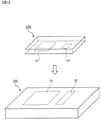
図1は、実施形態1における、電界結合型のワイヤレス電力伝送システムを構成する送電装置100と受電装置200の斜視図である。(Embodiment 1)
1. Configuration FIG. 1 is a perspective view of a
送電装置100は送電装置側パッシブ電極31と送電装置側アクティブ電極32を備え、受電装置200は受電装置側パッシブ電極41と受電装置側アクティブ電極42を備える。
The
送電装置100上に受電装置200を載置することによって、送電装置側パッシブ電極31と受電装置側パッシブ電極41とが対向し、送電装置側アクティブ電極32と受電装置側アクティブ電極42とが対向する。このとき、送電装置側パッシブ電極31及び送電装置側アクティブ電極32と、受電装置側パッシブ電極41及び受電装置側アクティブ電極42との間に結合容量Cmが生じる。送電装置100は、結合容量Cmを介した電界結合により受電装置200へワイヤレスで電力を伝送する。
By placing the
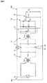
図2は、実施形態1のワイヤレス電力伝送システムの回路構成を示す図である。 FIG. 2 is a diagram illustrating a circuit configuration of the wireless power transmission system according to the first embodiment.
送電装置100は、電源回路10、送電装置側共振回路20、送電装置側パッシブ電極31、送電装置側アクティブ電極32を有する。
The
電源回路10は、所定の周波数の交流電圧を発生する。所定の周波数は、送電装置100から受電装置200への電力の伝送効率、ワイヤレス電力伝送システムにおける共振周波数との関係等を考慮して設定される。例えば、所定の周波数は100kHz〜数10MHzの間の高周波数に設定されるが、これに限定されるものではない。
The
送電装置側共振回路20は、電源回路10と、送電装置側パッシブ電極31及び送電装置側アクティブ電極32との間に接続されている。
The power transmission device
昇圧トランスTR1は、電源回路10の発生する電圧を昇圧し、この昇圧した電圧を送電装置側パッシブ電極31と送電装置側アクティブ電極32との間に印加する。昇圧トランスTR1は、電界結合による電力伝送の効率を向上させることを目的として設けられている。
The step-up transformer TR1 boosts the voltage generated by the
キャパシタCp1は、昇圧トランスTR1の出力端を短絡するように送電装置側パッシブ電極31と送電装置側アクティブ電極32との間に接続されている。キャパシタCp1は、部品として設けられてもよいし、送電装置100に含まれる配線等の寄生容量により構成してもよい。送電側では、昇圧トランスTR1のインダクタンス成分(リーケージインダクタンス)と、キャパシタCp1を含む容量で送電装置側共振回路20を構成している。
The capacitor Cp1 is connected between the power transmission device side
受電装置200は、受電装置側パッシブ電極41、受電装置側アクティブ電極42、受電装置側共振回路50及び負荷回路60を有する。
The
受電装置側パッシブ電極41及び受電装置側アクティブ電極42は、送電装置側パッシブ電極31及び送電装置側アクティブ電極32から結合容量Cmを介して電力を受ける。
The power receiving device side
負荷回路60は、ダイオードD1〜D4及びリップル除去用キャパシタCrを含む整流回路61と、整流回路61の二次側に接続された負荷RLを有する。負荷RLは、本実施形態では、整流後の電力により充電される二次電池である。二次電池は満充電状態に近づくとインピーダンスが増加する特性を有する。
The
受電装置側共振回路50は、負荷回路60と、受電装置側パッシブ電極41及び受電装置側アクティブ電極42との間に接続されている。受電装置側共振回路50は、降圧トランスTR2と、キャパシタCp2とを有する。
The power receiving device
降圧トランスTR2は、受電装置側パッシブ電極41と受電装置側アクティブ電極42との間の電圧(以下、適宜「受電電極間電圧」という)を降圧して負荷回路60に印加する。降圧トランスTR2は、電界結合による電力伝送の効率を、昇圧トランスTR1とで向上させることを目的として設けられている。
The step-down transformer TR2 steps down a voltage between the power receiving device side
キャパシタCp2は、受電装置側パッシブ電極41及び受電装置側アクティブ電極42との間に接続されている。キャパシタCp2は、部品として設けられてもよいし、受電装置200に含まれる配線等の寄生容量により構成してもよい。受電側では、降圧トランスTR2のインダクタンス成分と、キャパシタCp2を含む容量で受電装置側共振回路50を構成している。
The capacitor Cp2 is connected between the power receiving device side
特に、本実施形態においては、受電装置200の送電装置100からの引き離しに伴う受電電圧の上昇を抑制するため過電圧抑制手段70が設けられている。過電圧抑制手段70は、受電装置側共振回路50と並列に、すなわち降圧トランスTR2の出力端を短絡するように設けられている。過電圧抑制手段70は、インピーダンス素子で構成されている。インピーダンス素子のインピーダンスは、インピーダンス素子を接続しない場合に比べて一対の受電装置側パッシブ電極41と受電装置側アクティブ電極42との間の電圧の上昇を抑制するような値に設定される。
In particular, in the present embodiment, an
本実施形態では、過電圧抑制手段70をキャパシタCxにより構成している。キャパシタCxは、低周波側共振周波数と動作周波数の重なりを防止することで、受電装置200での高電圧の発生を抑制する。
In the present embodiment, the
2.過電圧抑制手段としてのキャパシタCx
過電圧抑制手段70としてのキャパシタCxについて説明する。キャパシタCxは、送電装置共振回路20と受電装置側共振回路50が結合容量により容量結合したときに発生する二つの共振周波数の内、低周波側の共振周波数を低周波側に所定のシフト量だけシフトさせる。キャパシタCxの容量は、低周波側の共振周波数を低周波側に所定のシフト量だけシフトさせるような値に設定される。本実施形態では、所定のシフト量は、受電装置200を送電装置100上に載置した状態から十分遠方に引き離す過程において低周波側の共振周波数が移動したとしても、低周波側の共振周波数が動作周波数f3と重なることがないような量に設定される。2. Capacitor Cx as overvoltage suppression means
The capacitor Cx as the
具体的には、キャパシタCxの容量は、送電電極31、32と受電電極41、42との間の結合容量Cmが、送電電極31、32と受電電極41、42とが通常送電時の所定の位置関係にあるときの値から略0に変化する過程において、受電装置側共振回路50により生じる低周波側及び高周波側の各共振周波数が動作周波数f3と重なることがないような値に設定されている。送電電極31、32と受電電極41、42とを容量結合させたときに生じる低周波側の共振周波数をf1、高周波側の共振周波数をf2、動作周波数をf3とする。キャパシタCxの容量は、送電電極31、32と受電電極41、42との間の結合容量Cmが、送電電極31、32と受電電極41、42とが通常送電時の所定の位置関係にあるときの値から略0に変化する過程において、f1<f3<f2の関係が満たされるように設定されている。ここで、送電電極31、32と受電電極41、42との間の結合容量Cmが略0とは、結合容量Cmが限りなく小さな値であることを意味する。
Specifically, the capacitance of the capacitor Cx is determined by a coupling capacitance Cm between the
なお、本実施形態では、送電装置100から受電装置200への送電の際、受電装置200は送電装置100上の所定位置に載置されているものとし、このときの送電装置と受電装置の位置関係を、通常送電時の所定の位置関係とする。所定の位置関係はこれに限定されない。例えば、受電装置200は送電装置100上の所定位置に載置されていなくても、受電装置200と送電装置100とが所定の位置関係にあることにより、送電装置100の送電電極41、42と受電装置200の受電電極31、32とが、通常送電時における所定の位置関係にあればよい。実施形態2〜5において同様である。
In this embodiment, when power is transmitted from the
また、所定のシフト量は上記の値に限定されない。例えば、低周波側の共振周波数を低周波側に所定のシフト量だけシフトすることで、受電装置200を送電装置100上に載置した状態から十分遠方に引き離す過程において低周波側の共振周波数が動作周波数f3と重なったときの受電電圧が受電装置200の破損を招かないような低い電圧となるのであれば、そのような量に設定されてもよい。
Further, the predetermined shift amount is not limited to the above value. For example, when the resonance frequency on the low frequency side is shifted by a predetermined shift amount to the low frequency side, the resonance frequency on the low frequency side is reduced in the process of separating the
キャパシタCxの容量をf1<f3<f2の関係を満たすように設定したときの具体例について図3を参照して説明する。図3は、二次電池がほぼ満充電状態となり負荷インピーダンスが高い状態における受電装置側アクティブ電極42と受電装置側パッシブ電極41との間の電圧の周波数特性の一例を示す図である。具体的には、図3(a)は、送電装置100と受電装置200とが過電圧抑制手段70としてのキャパシタCxが設けられている場合と設けられていない場合の特性を比較した図であり、実線はキャパシタCxが設けられている場合を示し、破線はキャパシタCxが設けられていない場合を示す。低周波側及び高周波側の共振周波数は、キャパシタCxが設けられていないときはf1o、f2oであるが、キャパシタCxが設けられているときはf1o、f2oよりも低いf1c、f2cとなる。つまり、キャパシタCxを設けることにより低周波側に移動する。このとき動作周波数f3は、2つの共振周波数f1c、f2cの中間の、受電電極間電圧の変化が少ない領域に位置する。そのため、受電装置200の送電装置100への載置位置のずれにより結合容量Cmが若干変化して、受電電極間電圧の周波数特性が多少変化したとしても、受電電極間電圧の変動は少なく、安定した電力伝送を行うことができる。また、この中間領域の受電電極間電圧は、効率的な電力伝送に必要な一定以上の大きさを有しているため、効率的な電力伝送を行うことができる。
A specific example when the capacitance of the capacitor Cx is set to satisfy the relationship of f1 <f3 <f2 will be described with reference to FIG. FIG. 3 is a diagram illustrating an example of a frequency characteristic of a voltage between the power receiving device side
図3(b)は、キャパシタCxが設けられている場合において、受電装置200が送電装置100から引き離される際の共振周波数の変化を示した図である。実線は受電装置200が送電装置100から引き離される前(結合容量Cmが第1の所定値のとき)を示し、破線は受電装置200が送電装置100から引き離された後(結合容量Cmが第2の所定値のとき)を示す。受電装置200が送電装置100から引き離されると、結合容量Cmが低下する。その結果、低周波側及び高周波側の共振周波数は、引き離される前のf1c、f2cからより高周波側のf1c′、f2c′に移動する。しかし、低周波側の共振周波数が動作周波数f3を超えて高周波側に移動することはない。また、高周波側の共振周波数は高周波側に、つまり動作周波数f3とは反対側に移動する。したがって、受電装置200の送電装置100からの引き離しによる結合容量Cmの変化(低下)により高周波側及び低周波側の各共振周波数が変化したとしても、動作周波数f3と、高周波側及び低周波側の共振周波数が一致する(重なる)ことはない。よって、共振周波数における高い受電電極間電圧(過電圧)が負荷回路60に印加されることがなく、負荷回路60の破損を防止することができる。
FIG. 3B is a diagram illustrating a change in resonance frequency when the
3.まとめ
本実施形態の電力伝送システムは、送電装置100と受電装置200との間でワイヤレスで電力を伝送する電力伝送システムである。送電装置100は、一対の送電電極31、32と、電源回路10と一対の送電電極31、32との間に設けられ、一対の送電電極31、32間に交流電圧を印加する送電装置側共振回路20と、を備える。受電装置200は、負荷回路60と、送電装置100の一対の送電電極31、32に対応して設けられ、一対の送電電極31、32との位置関係に応じた結合容量Cmを生じる一対の受電電極41、42と、負荷回路60と一対の受電電極41、42との間に設けられ、負荷回路60に交流電圧を印加する受電装置側共振回路50と、受電装置側共振回路50と並列に接続された過電圧抑制手段70とを備える。過電圧抑制手段70は、インピーダンス素子で構成される。インピーダンス素子のインピーダンスは、送電電極31、32と受電電極41、42との間の結合容量Cmが、送電電極31、32と受電電極41、42とが通常送電時の所定の位置関係にあるときの値から略0に変化する過程において、インピーダンス素子を接続しない場合に比べて一対の受電電極41、42間の電圧の上昇を抑制するような値に設定されている。3. Summary The power transmission system of the present embodiment is a power transmission system that wirelessly transmits power between the
この構成によれば、送電中に受電装置が送電装置から引き離されたときの送電装置100と受電装置200との間の距離の変化に伴い、受電装置200側における共振周波数が変化したとしても、共振周波数における高い受電電極間電圧が負荷回路60に印加されることがない。したがって、受電装置200及びそれに含まれる負荷回路60の破損を防止することができる。
According to this configuration, even if the resonance frequency on the
なお、特許文献1の電磁誘導型のワイヤレス電力伝送システムには、過電圧から受電装置の負荷回路を保護するための構成として、受電装置の受電コイルとその下流の整流回路との間にヒューズを設け、整流回路の出力電圧が過大になると、ヒューズを溶断させることが開示されている。しかし、一度溶断したヒューズは復元しないので、過電圧を再度抑制可能とするためには、ヒューズの交換等の手間が生じる。
In the electromagnetic induction type wireless power transmission system disclosed in
これに対して、本実施形態では、過電圧抑制手段70を、インピーダンス素子により構成したので、保護動作の際破損しにくい。よって、保護動作後も、特別な修理が必要なく、繰り返し保護動作を行うことができる。
On the other hand, in this embodiment, since the
また、本実施形態では、インピーダンス素子は、低周波側の共振周波数を所定のシフト量だけシフトさせる素子であり、所定のシフト量は、前記結合容量Cmが、送電電極31、32と受電電極41、42とが通常送電時の前記所定の位置関係にあるときの値から略ゼロに変化する過程において、低周波側の共振周波数が所定の送電周波数(動作周波数f3)と重なることがないような値に設定されている。
In the present embodiment, the impedance element is an element that shifts the resonance frequency on the low frequency side by a predetermined shift amount. The predetermined shift amount is determined by the coupling capacitance Cm by the
この構成によれば、過電圧抑制手段70により、受電装置側共振回路50により生じる各共振周波数と動作周波数f3とが重なることがない。これにより、共振周波数における高い受電電極間電圧が負荷回路60に印加されることがない。したがって、受電装置200及びそれに含まれる負荷回路60の破損を防止することができる。
According to this configuration, the resonance voltage generated by the power receiving device-
また、本実施形態では、キャパシタCxにより過電圧抑制手段70を構成している。この構成によれば、過電圧抑制手段70を容易にかつ小型に構成することができる。また、キャパシタCxを備えない従来の受電装置において、キャパシタCxを加えるだけで、つまり、従来の受電装置の構成を大きく変更することなく、過電圧を抑制することが可能となる。
In the present embodiment, the
また、本実施形態では、キャパシタCxの容量は、送電電極31、32と受電電極41、42とを容量結合させたときに受電装置側の共振回路50により生じる低周波側の共振周波数をf1、高周波側の共振周波数をf2、動作周波数をf3としたときにおいて、送電電極31、32と受電電極41、42との間の結合容量Cmが、送電電極31、32と受電電極41、42とが通常送電時の所定の位置関係にあるときの値から略0に変化する過程において、f1<f3<f2の関係が満たされるように設定されている。
Further, in the present embodiment, the capacitance of the capacitor Cx is the resonance frequency on the low frequency side generated by the
この構成によれば、送電装置100から受電装置200の引き離しにより送電電極31、32と受電電極41、42との間の結合容量Cmが、送電電極31、32と受電電極41、42とが通常送電時の所定の位置関係にあるときの値から略0に変化する過程において、低周波側及び高周波側の各共振周波数が動作周波数と重ならない。つまり、前述した負荷回路60の破損を防止する効果が得られる。また、低周波側共振周波数と高周波側共振周波数の中間の領域に動作周波数が存在することとなり、効率的な電力伝送に必要な受電電極間電圧を得ることができる。つまり、効率的な電力伝送を行うことができる。
According to this configuration, when the
また、本実施形態では、電源回路10と前記送電電極との間に昇圧トランスTR1が接続され、負荷回路60と受電電極41、42との間に降圧トランスTR2が接続されている。この構成によれば、送電電極31、32から受電電極41、42への電力伝送を高電圧で行うことができる。高電圧を用いることにより、伝送経路に流れる電流が比較的小さくても大きな電力を送ることができる。電流が小さければ、伝送経路における抵抗値による損失が小さくなる。そのため、電力伝送を高効率で行うことができる。
In the present embodiment, the step-up transformer TR1 is connected between the
なお、本実施形態では、キャパシタCxの容量は、送電電極31、32と受電電極41、42との間の結合容量Cmが、送電電極31、32と受電電極41、42とが通常送電時の所定の位置関係にあるときの値から略0に変化する過程において、受電装置側共振回路50により生じる低周波側及び高周波側の各共振周波数が動作周波数f3と重ならないようにする値に設定したが、これに限らない。例えば、キャパシタCxの容量は、送電電極31、32と受電電極41、42とが通常送電時の所定の位置関係にあるときの値から減少する過程において、受電装置側共振回路50により生じる低周波側及び高周波側の各共振周波数が動作周波数f3と重なったとしても受電電極間電圧が受電装置200に破損を生じさせる程度の高い電圧に到達しないようにする値に、設定してもよい。
In the present embodiment, the capacitance of the capacitor Cx is the coupling capacitance Cm between the
(実施形態2)
実施形態2について説明する。図4は、実施形態2に係るワイヤレス電力伝送システムの回路構成を示す図である。(Embodiment 2)
Embodiment 2 will be described. FIG. 4 is a diagram illustrating a circuit configuration of the wireless power transmission system according to the second embodiment.
本実施形態では、過電圧抑制手段70をインダクタLxにより構成している。その他の構成は実施形態1と同一である。インダクタLxは、低周波側共振周波数と動作周波数の重なりを防止することで、受電装置200での高電圧の発生を抑制する。
In the present embodiment, the
過電圧抑制手段70としてのインダクタLxについて説明する。インダクタLxは、受電装置側共振回路50により生じる低周波側及び高周波側の共振周波数を高周波側にシフトさせる。インダクタLxのインダクタンスは、低周波側の共振周波数を高周波側に所定のシフト量だけシフトさせるような値に設定される。本実施形態では、所定のシフト量は、受電装置200を送電装置100上に載置した状態から十分遠方に引き離す過程において低周波側の共振周波数が移動したとしても、低周波側の共振周波数が動作周波数f3と重なることがないような量に設定される。具体的には、インダクタLxのインダクタンスは、送電電極31、32と受電電極41、42との間の結合容量Cmが、送電電極31、32と受電電極41、42とが通常送電時の所定の位置関係にあるときの値から略0に変化する過程において、受電装置側共振回路50により生じる低周波側及び高周波側の各共振周波数が動作周波数f3と重なることがないような値に設定されている。送電電極31、32と受電電極41、42との容量結合による低周波側の共振周波数をf1、高周波側の共振周波数をf2、動作周波数をf3とする。インダクタLxのインダクタンスは、送電電極31、32と受電電極41、42とが通常送電時の所定の位置関係にあるときの値から略0に変化する過程において、f3<f1<f2の関係が満たされるように設定されている。
The inductor Lx as the
インダクタLxのインダクタンスをf3<f1<f2の関係を満たすように設定したときの具体例について図5を参照して説明する。図5は、負荷RL(二次電池)がほぼ満充電状態となり負荷インピーダンスが高くなった状態における受電電極間電圧の周波数特性の一例を示す図である。具体的には、図5(a)は、過電圧抑制手段70としてのインダクタLxが設けられている場合と設けられていない場合の特性を比較した図であり、実線はインダクタLxが設けられている場合を示し、破線はインダクタLxが設けられていない場合を示す。低周波側及び高周波側の共振周波数は、インダクタLxが設けられていないときはf1o、f2oであるが、インダクタLxが設けられているときはf1o、f2oよりも高いf1i、f2i(図5(a)においてf2iはf1iよりも高周波側の図外に存在する)である。つまり、インダクタLxを設けることにより高周波側に移動する。このとき動作周波数f3は、低周波側の共振周波数f1iよりも若干低い周波数となっている。インダクタLxを設けることにより低周波側の共振周波数f1iにおける受電電極間電圧は、インダクタLxが設けられていない場合よりも大きく低下し、効率的な電力伝送に必要な一定以上の大きさとなっている。そのため、効率的な電力伝送を行うことができる。また、低周波側の共振周波数f1iにおける受電電極間電圧の変化は、インダクタLxが設けられていない場合よりも緩やかになっている。そのため、受電電極間電圧の周波数特性が多少変化したとしても、受電電極間電圧の変動は少なく、安定した電力伝送を行うことができる。
A specific example when the inductance of the inductor Lx is set so as to satisfy the relationship of f3 <f1 <f2 will be described with reference to FIG. FIG. 5 is a diagram illustrating an example of frequency characteristics of the voltage between the receiving electrodes when the load RL (secondary battery) is almost fully charged and the load impedance is high. Specifically, FIG. 5A is a diagram comparing characteristics when the inductor Lx as the
図5(b)は、インダクタLxが設けられている場合において、受電装置200が送電装置100から引き離される際の共振周波数の変化を示した図である。実線は受電装置200が送電装置100から引き離される前を示し、破線は受電装置200が送電装置100から引き離された後を示す。受電装置200が送電装置100から引き離されると、結合容量Cmの低下により、低周波側及び高周波側の共振周波数(高周波側の共振周波数は図5(b)において図外に存在する)は、引き離される前のf1i、f2i(図5(b)においてf2iはf1iよりも高周波側の図外に存在する)からf1i′、f2i′(図5(b)においてf2i′はf1i′よりも高周波側の図外に存在する)に高周波側へ、つまり動作周波数f3とは反対側に移動する。したがって、受電装置200の送電装置100からの引き離しによる結合容量Cmの変化(低下)により高周波側及び低周波側の共振周波数が変化したとしても、動作周波数f3と、高周波側及び低周波側の共振周波数が重なることはない。よって、共振周波数における高い受電電極間電圧(過電圧)が負荷回路60に印加されることがなく、負荷回路60の破損を防止することができる。
FIG. 5B is a diagram illustrating a change in the resonance frequency when the
また、本実施形態によれば、インダクタLxにより過電圧抑制手段70を構成していることにより、保護動作の際破損しにくい。よって、保護動作後も、特別な修理が必要なく、繰り返し保護動作を行うことができる。また、過電圧抑制手段70を容易にかつ小型に構成することができる。
Further, according to the present embodiment, since the
なお、本実施形態では、インダクタLxのインダクタンスは、送電電極31、32と受電電極41、42との間の結合容量Cmが、送電電極31、32と受電電極41、42とが通常送電時の所定の位置関係にあるときの値から略0まで変化する過程において、受電装置側共振回路50により生じる低周波側及び高周波側の各共振周波数が動作周波数f3と重ならないようにする値に設定したが、これに限らない。例えば、インダクタLxのインダクタンスは、送電電極31、32と受電電極41、42とが通常送電時の所定の位置関係にあるときの値から減少する過程において、受電装置側共振回路50により生じる低周波側及び高周波側の各共振周波数が動作周波数f3と重なったとしても受電電極間電圧が受電装置200に破損を生じさせる程度の高い電圧に到達しないようにする値に、設定してもよい。
In the present embodiment, the inductance of the inductor Lx is such that the coupling capacitance Cm between the
なお、所定のシフト量は上記の値に限定されない。例えば、低周波側の共振周波数を高周波側に所定のシフト量だけシフトすることで、受電装置200を送電装置100上に載置した状態から十分遠方に引き離す過程において低周波側の共振周波数が動作周波数f3と重なったときの受電電圧が受電装置200の破損を招かないような低い電圧となるのであれば、そのような量に設定されてもよい。
The predetermined shift amount is not limited to the above value. For example, by shifting the resonance frequency on the low frequency side by a predetermined shift amount to the high frequency side, the resonance frequency on the low frequency side operates in the process of separating the
(実施形態3)
実施形態3について説明する。図6は、実施形態3に係るワイヤレス電力伝送システムの回路構成を示す図である。(Embodiment 3)
A third embodiment will be described. FIG. 6 is a diagram illustrating a circuit configuration of the wireless power transmission system according to the third embodiment.
本実施形態では、過電圧抑制手段70を、抵抗Rx(インピーダンス素子)により構成している。その他の構成は実施形態1と同一である。抵抗Rxは、抵抗Rxを接続しない場合に比べて、受電装置200の受電装置側共振回路50から見た負荷装置60側のインピーダンスを低下させる素子である、これにより、受電装置200での高電圧の発生を抑制する。
In this embodiment, the overvoltage suppression means 70 is comprised by resistance Rx (impedance element). Other configurations are the same as those of the first embodiment. The resistor Rx is an element that lowers the impedance on the
抵抗Rxの抵抗値は、低周波側共振周波数及び高低周波側共振周波数が変化して動作周波数と一致したとしても、受電電極間電圧が受電装置200に異常を生じさせる程度の高い電圧に到達しないようする値に設定する。抵抗Rxの抵抗値は、例えば受電装置側共振回路50のインピーダンスよりも小さい値に設定され、低周波側共振周波数及び高低周波側共振周波数における受電装置側共振回路50の二次側のインピーダンスを低下させる。例えば、抵抗Rxの抵抗値は、10〜100Ωに設定する。これにより、受電装置側共振回路50の二次側の電圧が低下して、負荷回路60に印加される電圧が低下し、負荷回路60に損傷を生じさせることを防止する。
The resistance value of the resistor Rx does not reach such a high voltage that the voltage between the power receiving electrodes causes an abnormality in the
このように過電圧抑制手段70を抵抗Rxにより構成することにより、システム全体としてのインピーダンスを抵抗Rxが存在しない場合よりも低くすることができる。特に抵抗Rxの抵抗値を10〜100Ωに設定することにより、受電装置側共振回路50の二次側のインピーダンスを、抵抗Rxが存在しない場合よりも確実に低くすることができる。したがって、受電装置200の送電装置100からの引き離しによる結合容量Cmの変化(低下)により高周波側及び低周波側の共振周波数が変化して、動作周波数と一致したとしても、高い受電電極間電圧(過電圧)が負荷回路60に印加されることがない。よって、負荷回路60の破損を防止することができる。
By configuring the overvoltage suppressing means 70 with the resistor Rx as described above, the impedance of the entire system can be made lower than when the resistor Rx is not present. In particular, by setting the resistance value of the resistor Rx to 10 to 100Ω, the impedance on the secondary side of the power receiving device
また、本実施形態によれば、抵抗Rxにより過電圧抑制手段70を構成していることにより、保護動作の際破損しにくい。よって、保護動作後も、特別な修理が必要なく、繰り返し保護動作を行うことができる。また、過電圧抑制手段70を容易にかつ小型に構成することができる。
Further, according to the present embodiment, since the
(実施形態4)
実施形態4について説明する。図7は、実施形態4に係るワイヤレス電力伝送システムの回路構成を示す図である。(Embodiment 4)
A fourth embodiment will be described. FIG. 7 is a diagram illustrating a circuit configuration of the wireless power transmission system according to the fourth embodiment.
本実施形態では、過電圧抑制手段70をキャパシタCxにより構成するとともに、キャパシタCxに直列にスイッチング素子SWを設けている。また、整流回路61での整流後の負荷RLへの入力電圧(以下、適宜「負荷入力電圧」という)を検出し、検出した負荷入力電圧に基づいてスイッチング素子SWのON/OFFを制御する制御回路80を設けている。その他の構成は実施形態1と同一である。
In the present embodiment, the
制御回路80は、検出した負荷入力電圧が所定電圧以上より高いときは、スイッチング素子SWをONに制御し、それ以外のときはスイッチング素子SWをOFFに制御する。所定電圧は、負荷回路60の耐電圧等に基づき適宜設定すればよい。
The
なお、キャパシタCxの容量は、実施形態1同様に設定されている。 Note that the capacitance of the capacitor Cx is set as in the first embodiment.
このような構成によれば、受電装置200を送電装置100から引き離すことにより結合容量Cmが減少して低周波側の共振周波数が動作周波数に接近し、負荷入力電圧が所定電圧以上に上昇すると、スイッチング素子SWがONに制御され、キャパシタCxが接続される。これにより、低周波側及び高周波側の各共振周波数がそれぞれ低周波側に移動する。その結果、低周波側の共振周波数と動作周波数との重なりを防止でき、前記各実施形態同様、共振周波数における高い受電電極間電圧(過電圧)が負荷回路60に印加されることがなく、負荷回路60の破損を防止することができる。
According to such a configuration, when the
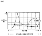
図8は、実施形態4に係るワイヤレス電力伝送システムにおける、結合容量Cmに対する負荷回路入力電圧の特性を示す図である。破線はキャパシタCx及びスイッチング素子SWが設けられていない場合の特性である。本実施形態によれば、負荷回路入力電圧が所定電圧以上に上昇すると、スイッチング素子SWがONに制御されることにより、負荷入力電圧の跳ね上がりを抑え、負荷入力電圧を安定化できる。 FIG. 8 is a diagram illustrating the characteristics of the load circuit input voltage with respect to the coupling capacitance Cm in the wireless power transmission system according to the fourth embodiment. A broken line is a characteristic when the capacitor Cx and the switching element SW are not provided. According to this embodiment, when the load circuit input voltage rises to a predetermined voltage or higher, the switching element SW is controlled to be ON, thereby suppressing the jump of the load input voltage and stabilizing the load input voltage.
以上のように本実施形態では、実施形態1の構成に加え、負荷回路60を構成する整流回路61の二次側の負荷入力電圧を検出するとともに、検出された負荷入力電圧が所定の電圧より高かった場合に、スイッチング素子SWをオンにするための制御信号を出力する制御回路80(電圧検出回路)と、制御信号を受けてキャパシタCxの接続をオンに切り替えるスイッチング素子SWと、をさらに備える。
As described above, in the present embodiment, in addition to the configuration of the first embodiment, the load input voltage on the secondary side of the
これにより、負荷入力電圧が所定電圧以上に上昇すると、スイッチング素子SWがONに制御されることにより、負荷入力電圧の跳ね上がりを抑え、負荷入力電圧を安定化できる。 As a result, when the load input voltage rises to a predetermined voltage or higher, the switching element SW is controlled to be ON, thereby suppressing the jump of the load input voltage and stabilizing the load input voltage.
ここで、通常送電時においてもキャパシタCxが接続されていると、受電電極間電圧が低くなり電力伝送効率が低下する。しかし、本実施形態によれば、負荷入力電圧が所定電圧以上に上昇したときのみ、キャパシタCxを接続するので、伝送効率の低下を防止できる。 Here, when the capacitor Cx is connected even during normal power transmission, the voltage between the power receiving electrodes is lowered, and the power transmission efficiency is lowered. However, according to the present embodiment, since the capacitor Cx is connected only when the load input voltage rises above a predetermined voltage, it is possible to prevent a reduction in transmission efficiency.
(実施形態5)
実施形態5について説明する。図9は、実施形態5に係るワイヤレス電力伝送システムの回路構成を示す図である。(Embodiment 5)
Embodiment 5 will be described. FIG. 9 is a diagram illustrating a circuit configuration of a wireless power transmission system according to the fifth embodiment.
本実施形態では、過電圧抑制手段70を、直列に設けた2個のキャパシタCx1、Cx2により構成するとともに、これらのキャパシタCx1、Cx2の間にスイッチング素子SWを設けている。また、整流回路61での整流後の負荷入力電圧を検出するとともに、検出した電圧に基づいてスイッチング素子SWのON/OFFを制御する制御回路80を設けている。その他の構成は実施形態1と同一である。
In this embodiment, the
このような構成により、実施形態4と同様の効果が得られる。なお、実施形態4では過電圧抑制手段70を1個のキャパシタCxで構成した場合について、実施形態5では過電圧抑制手段70を2個のキャパシタCx1、Cx2で構成した場合について説明した。しかし、過電圧抑制手段70を3個以上の数のキャパシタで構成することも可能である。
With such a configuration, the same effect as in the fourth embodiment can be obtained. In the fourth embodiment, the case where the
図10は、制御回路80のより具体的な構成を示す図である。
FIG. 10 is a diagram showing a more specific configuration of the
降圧トランスTR2の一方の出力端T1にキャパシタCx1及びスイッチング素子SW1の直列回路が接続され、他方の出力端T2にキャパシタCx2及びスイッチング素子SW2の直列回路が接続されている。 A series circuit of the capacitor Cx1 and the switching element SW1 is connected to one output terminal T1 of the step-down transformer TR2, and a series circuit of the capacitor Cx2 and the switching element SW2 is connected to the other output terminal T2.
制御回路80は、比較器COMP、電圧源Vc等を備えている。比較器COMPは、電圧源Vcの出力電圧を分圧した基準電圧と、整流回路61のリップル除去用コンデンサCrの電圧とを比較する。そして、比較器COMPは、リップル除去用コンデンサCrの電圧が基準電圧以上となると、各スイッチング素子SW1、SW2にON信号を出力する。
The
このような構成により、制御回路80を簡単な構成で実現できる。この回路のほか、ヒステリシスを持たせることで動作を安定化させることができる。スイッチング素子としてFETを用いたが、これに限定されるものでなく、電磁リレーなどのスイッチング素子も適用できる。
With such a configuration, the
(その他の実施形態) (Other embodiments)
なお、実施形態4、5で説明したスイッチング素子を有する構成は、引き離し時の電圧変動を抑える目的以外にも適用可能である。例えば、正常動作時にスイッチング素子を制御することにより、共振条件を変化させることができる。すなわち、後段の回路に出力する電圧を変化させ後段の回路の入力電圧の範囲を狭くしたい時のリミッタとしても用いることができる。 Note that the configuration having the switching element described in the fourth and fifth embodiments can be applied for purposes other than the purpose of suppressing voltage fluctuations during separation. For example, the resonance condition can be changed by controlling the switching element during normal operation. That is, it can also be used as a limiter when it is desired to change the voltage output to the subsequent circuit to narrow the input voltage range of the subsequent circuit.
実施形態4、5では、過電圧抑制手段としてのインピーダンス素子をキャパシタで構成した場合について説明したが、実施形態4〜5の思想は、過電圧抑制手段としてのインピーダンス素子がインダクタや抵抗である場合にも適用可能である。 In the fourth and fifth embodiments, the case where the impedance element as the overvoltage suppressing means is configured by a capacitor has been described. However, the idea of the fourth to fifth embodiments can be applied to the case where the impedance element as the overvoltage suppressing means is an inductor or a resistor. Applicable.
上記各実施形態では、負荷回路としての二次電池がほぼ満充電状態となることにより負荷インピーダンスが高くなる場合について説明したが、本発明はこれに限定されない。例えば、負荷回路が二次電池ではないが負荷インピーダンスが定常的にあるいは一時的に高くなるものであることにより、図13(b)のような特性を示すものに対しても本発明は適用可能である。
上記各実施形態では降圧トランスTR2の二次側に並列に過電圧抑制手段70を設けたが、降圧トランスTR2の一次側に設けてもよい。トランスTR2の一次側に過電圧抑制手段70を設ける場合には、過電圧抑制手段70のキャパシタを高耐電圧仕様のものにする必要がある。In each of the above embodiments, the case has been described where the load impedance becomes high when the secondary battery as the load circuit is almost fully charged, but the present invention is not limited to this. For example, although the load circuit is not a secondary battery, the present invention can be applied to a battery that exhibits characteristics as shown in FIG. 13B because the load impedance is constantly or temporarily increased. It is.
In each of the above embodiments, the
10 電源回路
20 送電装置側共振回路
31 送電装置側パッシブ電極
32 送電装置側アクティブ電極
41 受電装置側パッシブ電極
42 受電装置側アクティブ電極
50 受電装置側共振回路
60 負荷回路
61 整流回路
70 過電圧抑制手段
80 制御回路
100 送電装置
200 受電装置
Cp1 キャパシタ
Cp2 キャパシタ
Cx、Cx1、Cx2 キャパシタ
Lx インダクタ
Rx 抵抗
RL 負荷
SW、SW1、SW2 スイッチング素子
TR1 昇圧トランス
TR2 降圧トランスDESCRIPTION OF
Claims (12)
負荷回路と、
前記送電装置の前記少なくとも一対の送電電極に対応して設けられ、前記少なくとも一対の送電電極との位置関係に応じた結合容量を生じる少なくとも一対の受電電極と、
前記負荷回路と前記少なくとも一対の受電電極との間に接続され、前記負荷回路に交流電圧を印加する共振回路と、
前記受電装置側共振回路に対して並列に接続された過電圧抑制手段とを備え、
前記過電圧抑制手段は、インピーダンス素子で構成され、
前記インピーダンス素子のインピーダンスは、前記送電電極と前記受電電極との結合容量が、前記送電電極と前記受電電極とが通常送電時の所定の位置関係にあるときの値から略0に変化する過程において、前記インピーダンス素子を接続しない場合に比べて前記少なくとも一対の受電電極間の電圧の上昇を抑制するような値に設定される、
受電装置。 A power supply circuit that generates an AC voltage of a predetermined power transmission frequency, at least a pair of power transmission electrodes, and is connected between the power supply circuit and the at least a pair of power transmission electrodes, and an AC voltage is applied between the at least a pair of power transmission electrodes. A power receiving device for receiving electric power transmitted wirelessly from a power transmitting device comprising:
A load circuit;
At least a pair of power receiving electrodes provided corresponding to the at least a pair of power transmission electrodes of the power transmission device, and generating a coupling capacity according to a positional relationship with the at least the pair of power transmission electrodes;
A resonance circuit connected between the load circuit and the at least one pair of power receiving electrodes, and applying an alternating voltage to the load circuit;
And a overvoltage suppression means connected in parallel to the power receiving apparatus side resonant circuit,
The overvoltage suppressing means is composed of an impedance element,
The impedance of the impedance element is a process in which the coupling capacitance between the power transmitting electrode and the power receiving electrode changes from a value when the power transmitting electrode and the power receiving electrode are in a predetermined positional relationship during normal power transmission to substantially zero. , Is set to a value that suppresses an increase in voltage between the at least one pair of power receiving electrodes as compared to the case where the impedance element is not connected,
Power receiving device.
前記所定のシフト量は、前記送電電極と前記受電電極との結合容量が、前記送電電極と前記受電電極とが通常送電時の所定の位置関係にあるときの値から略ゼロに変化する過程において、前記低周波側の共振周波数が前記所定の送電周波数と重なることがないような値に設定される、
請求項1に記載の受電装置。 The impedance element shifts the resonance frequency on the low frequency side by a predetermined shift amount, out of two resonance frequencies generated when the power transmission device side resonance circuit and the power reception device side resonance circuit are capacitively coupled by the coupling capacitance. Element to be
The predetermined shift amount is a process in which the coupling capacitance between the power transmission electrode and the power reception electrode changes from a value when the power transmission electrode and the power reception electrode are in a predetermined positional relationship during normal power transmission to substantially zero. The low-frequency resonance frequency is set to a value that does not overlap the predetermined power transmission frequency.
The power receiving device according to claim 1.
請求項1に記載の受電装置。 The impedance element is an element that lowers the impedance on the load device side viewed from the resonance circuit of the power receiving device, compared to a case where the impedance device is not connected.
The power receiving device according to claim 1.
請求項1または2に記載の受電装置。 The overvoltage suppressing means is a capacitor;
The power receiving device according to claim 1.
前記送電電極と前記受電電極とを容量結合させたときに当該受電装置側の前記共振回路により生じる前記低周波側の共振周波数をf1、高周波側の共振周波数をf2、前記所定の送電周波数をf3としたときに、
前記送電電極と前記受電電極との結合容量が前記送電電極と前記受電電極とが通常送電時の所定の位置関係にあるときの値から略0に変化する過程において、f1<f3<f2の関係が満たされるように設定されている。
請求項4に記載の受電装置。 The capacitance of the capacitor is
When the power transmitting electrode and the power receiving electrode are capacitively coupled, the low frequency side resonance frequency generated by the resonance circuit on the power receiving device side is f1, the high frequency side resonance frequency is f2, and the predetermined power transmission frequency is f3. And when
In a process in which the coupling capacitance between the power transmission electrode and the power reception electrode changes from a value when the power transmission electrode and the power reception electrode are in a predetermined positional relationship during normal power transmission to substantially 0, a relationship of f1 <f3 <f2 Is set to be satisfied.
The power receiving device according to claim 4.
請求項1または2に記載の受電装置。 The overvoltage suppressing means is an inductor;
The power receiving device according to claim 1.
前記送電電極と前記受電電極とを容量結合させたときに当該受電装置側の前記共振回路により生じる前記低周波側の共振周波数をf1、高周波側の共振周波数をf2、前記所定の送電周波数をf3としたときに、前記送電電極と前記受電電極との結合容量が前記送電電極と前記受電電極とが通常送電時の所定の位置関係にあるときの値から略0まで変化する過程において、f3<f1<f2の関係が満たされるように設定されている、
請求項6に記載の受電装置。 The inductance of the inductor is
When the power transmitting electrode and the power receiving electrode are capacitively coupled, the low frequency side resonance frequency generated by the resonance circuit on the power receiving device side is f1, the high frequency side resonance frequency is f2, and the predetermined power transmission frequency is f3. In the process in which the coupling capacitance between the power transmitting electrode and the power receiving electrode changes from a value when the power transmitting electrode and the power receiving electrode are in a predetermined positional relationship during normal power transmission to approximately 0, f3 < set so that the relationship of f1 <f2 is satisfied,
The power receiving device according to claim 6.
請求項1または3に記載の受電装置。 The overvoltage suppressing means is a resistor;
The power receiving device according to claim 1 or 3.
請求項8に記載の受電装置。 The resistance value of the resistor is set to 10 to 100Ω,
The power receiving device according to claim 8.
前記負荷回路を構成する整流回路の二次側の電圧を検出し、検出された電圧が所定の電圧より高いときに、前記スイッチング素子をオンに制御する制御回路が設けられている、
請求項1〜9のいずれか1項に記載の受電装置。 A switching element is provided in series with the overvoltage suppressing means,
A control circuit is provided that detects the voltage on the secondary side of the rectifier circuit that constitutes the load circuit, and controls the switching element to be turned on when the detected voltage is higher than a predetermined voltage.
The power receiving device according to any one of claims 1 to 9.
前記受電装置側共振回路は降圧トランスを含んで構成される、
請求項1〜10のいずれか1項に記載の受電装置。 The power transmission device side resonance circuit includes a step-up transformer,
The power receiving device side resonance circuit includes a step-down transformer,
The power receiving device according to claim 1.
請求項1〜11のいずれか1項に記載の受電装置と、を含む
電力伝送システム。 A power supply circuit that generates an AC voltage having a predetermined frequency, at least a pair of power transmission electrodes, and is connected between the power supply circuit and the at least one pair of power transmission electrodes, and applies an AC voltage between the at least a pair of power transmission electrodes. A power transmission device comprising a resonance circuit;
A power transmission system comprising: the power receiving device according to claim 1.
Priority Applications (1)
| Application Number | Priority Date | Filing Date | Title |
|---|---|---|---|
| JP2014507314A JP5590268B2 (en) | 2012-03-26 | 2012-11-01 | Electric field coupled wireless power transmission system and power receiving apparatus used therefor |
Applications Claiming Priority (4)
| Application Number | Priority Date | Filing Date | Title |
|---|---|---|---|
| JP2012069819 | 2012-03-26 | ||
| JP2012069819 | 2012-03-26 | ||
| JP2014507314A JP5590268B2 (en) | 2012-03-26 | 2012-11-01 | Electric field coupled wireless power transmission system and power receiving apparatus used therefor |
| PCT/JP2012/078389 WO2013145403A1 (en) | 2012-03-26 | 2012-11-01 | Electric-field-coupled wireless electric power transmission system, and power receiving device using same |
Publications (2)
| Publication Number | Publication Date |
|---|---|
| JP5590268B2 true JP5590268B2 (en) | 2014-09-17 |
| JPWO2013145403A1 JPWO2013145403A1 (en) | 2015-12-10 |
Family
ID=49258742
Family Applications (1)
| Application Number | Title | Priority Date | Filing Date |
|---|---|---|---|
| JP2014507314A Active JP5590268B2 (en) | 2012-03-26 | 2012-11-01 | Electric field coupled wireless power transmission system and power receiving apparatus used therefor |
Country Status (5)
| Country | Link |
|---|---|
| US (1) | US9831917B2 (en) |
| JP (1) | JP5590268B2 (en) |
| CN (1) | CN104126264B (en) |
| GB (1) | GB2515221B (en) |
| WO (1) | WO2013145403A1 (en) |
Families Citing this family (17)
| Publication number | Priority date | Publication date | Assignee | Title |
|---|---|---|---|---|
| JP5862844B2 (en) * | 2013-10-09 | 2016-02-16 | 株式会社村田製作所 | Wireless power transmission system |
| TWI513135B (en) * | 2013-11-18 | 2015-12-11 | Richtek Technology Corp | Power management unit and wireless power system thereof |
| CN110362182B (en) | 2014-01-30 | 2023-07-25 | 索尼公司 | Electronic equipment |
| US9673658B2 (en) * | 2014-03-06 | 2017-06-06 | Samsung Electro-Mechanics Co., Ltd. | Non-contact capacitive coupling type power charging apparatus and non-contact capacitive coupling type battery apparatus |
| JP2016032425A (en) * | 2014-07-30 | 2016-03-07 | 株式会社ExH | Power supply system and movable body therefor |
| CN207124491U (en) * | 2015-02-26 | 2018-03-20 | 株式会社村田制作所 | Voltage detecting circuit, power transmission device and electrical power transmission system |
| US9640976B2 (en) | 2015-02-26 | 2017-05-02 | Ut-Battelle, Llc | Overvoltage protection system for wireless power transfer systems |
| CN104979914B (en) * | 2015-06-11 | 2018-05-25 | 昆明理工大学 | A kind of field coupling formula radio energy transmission system |
| JP6890379B2 (en) * | 2016-02-17 | 2021-06-18 | 株式会社Fuji | Non-contact power supply device |
| JP6986712B2 (en) * | 2016-12-22 | 2021-12-22 | パナソニックIpマネジメント株式会社 | Mobile and wireless power transfer systems |
| CN108539871B (en) * | 2017-03-02 | 2021-10-08 | 泰达电子股份有限公司 | Wireless power transmission device |
| WO2018163177A1 (en) | 2017-03-07 | 2018-09-13 | Powermat Technologies Ltd. | System for wireless power charging |
| JP7406376B2 (en) * | 2017-03-07 | 2023-12-27 | パワーマット テクノロジーズ リミテッド | System for wireless power charging |
| CN108808868A (en) * | 2017-05-05 | 2018-11-13 | 国美科技有限公司 | Wireless charging receiver with voltage protection |
| US11139690B2 (en) * | 2018-09-21 | 2021-10-05 | Solace Power Inc. | Wireless power transfer system and method thereof |
| WO2020175584A1 (en) * | 2019-02-28 | 2020-09-03 | パナソニックIpマネジメント株式会社 | Wireless electric power transmission system, power transmission device, power reception device, and mobile body |
| TWI794795B (en) * | 2021-04-26 | 2023-03-01 | 國立陽明交通大學 | Inductive resonant wireless charging system, resonant wireless charging transmitting device, wireless charging relay device and inductive wireless charging receiving device |
Family Cites Families (11)
| Publication number | Priority date | Publication date | Assignee | Title |
|---|---|---|---|---|
| GB2321726A (en) * | 1997-01-30 | 1998-08-05 | Motorola Inc | Apparatus and method for regulating power on a contactless portable data carrier |
| JP2001268823A (en) * | 2000-03-16 | 2001-09-28 | Aichi Electric Co Ltd | Non-contact feeder system |
| JP5054113B2 (en) * | 2007-09-17 | 2012-10-24 | 秀雄 菊地 | Inductive power transmission circuit |
| JP2009118587A (en) | 2007-11-02 | 2009-05-28 | Meleagros Corp | Power transmitter |
| CN201185355Y (en) * | 2008-04-24 | 2009-01-21 | 武汉大学 | High voltage line induction electricity-taking apparatus |
| JP4557049B2 (en) * | 2008-06-09 | 2010-10-06 | ソニー株式会社 | Transmission system, power supply apparatus, power reception apparatus, and transmission method |
| CN102754306B (en) * | 2010-05-28 | 2014-12-24 | 株式会社村田制作所 | Power transmission system |
| JP5177187B2 (en) * | 2010-08-10 | 2013-04-03 | 株式会社村田製作所 | Power transmission system |
| JP5093386B2 (en) * | 2010-08-25 | 2012-12-12 | 株式会社村田製作所 | Power transmission device and power transmission system |
| US8830637B2 (en) * | 2010-08-31 | 2014-09-09 | Texas Instruments Incorporated | Methods and apparatus to clamp overvoltages for alternating current systems |
| EP2707940B1 (en) * | 2011-05-13 | 2016-08-10 | Murata Manufacturing Co., Ltd. | Power transmission device and power transfer system |
-
2012
- 2012-11-01 JP JP2014507314A patent/JP5590268B2/en active Active
- 2012-11-01 WO PCT/JP2012/078389 patent/WO2013145403A1/en active Application Filing
- 2012-11-01 CN CN201280070182.9A patent/CN104126264B/en active Active
- 2012-11-01 GB GB1416991.6A patent/GB2515221B/en active Active
-
2014
- 2014-08-21 US US14/465,144 patent/US9831917B2/en active Active
Also Published As
| Publication number | Publication date |
|---|---|
| GB201416991D0 (en) | 2014-11-12 |
| WO2013145403A1 (en) | 2013-10-03 |
| GB2515221A (en) | 2014-12-17 |
| CN104126264A (en) | 2014-10-29 |
| US20140361639A1 (en) | 2014-12-11 |
| US9831917B2 (en) | 2017-11-28 |
| CN104126264B (en) | 2017-05-03 |
| JPWO2013145403A1 (en) | 2015-12-10 |
| GB2515221B (en) | 2018-01-24 |
Similar Documents
| Publication | Publication Date | Title |
|---|---|---|
| JP5590268B2 (en) | Electric field coupled wireless power transmission system and power receiving apparatus used therefor | |
| JP5811292B2 (en) | Power transmission system | |
| JP5375322B2 (en) | Charger | |
| JP6677306B2 (en) | Power receiving device and wireless power supply system | |
| US9559527B2 (en) | Discharging circuit, image forming apparatus having the discharging circuit, and power supply unit | |
| JP6003172B2 (en) | Power supply device and power supply system | |
| JP5862844B2 (en) | Wireless power transmission system | |
| JP6007561B2 (en) | Power supply device and power supply system | |
| JP6127668B2 (en) | Electronic equipment and power supply system | |
| US9246399B2 (en) | Power supply system and control method thereof | |
| CN112542899A (en) | Advanced overvoltage protection strategy for wireless power transfer | |
| WO2014178345A1 (en) | Power supply system and resonant circuit | |
| JP5300337B2 (en) | Power supply device and lighting fixture | |
| US9343225B2 (en) | Power receiving device, power transmitting device and control device | |
| JP2019216592A (en) | Method of operating wireless power receiver and wireless power receiver using the same | |
| JP2017063526A (en) | Non-contact power transmission device | |
| JP2013102665A (en) | Power-feed device and power-feed system | |
| JP7205169B2 (en) | Contactless power supply | |
| US20200365316A1 (en) | Wireless Power Transmission with Current-Limiting Coil | |
| WO2018061932A1 (en) | Power source apparatus | |
| JP6172088B2 (en) | Resonant current limiter | |
| JP2012095446A (en) | Power supply unit and withstand voltage test method therefor | |
| JP6782474B2 (en) | Thermoelectric conversion element output control device | |
| JP6496678B2 (en) | Power receiving device | |
| JP2014017893A (en) | Non-contact power transmission device |
Legal Events
| Date | Code | Title | Description |
|---|---|---|---|
| TRDD | Decision of grant or rejection written | ||
| A01 | Written decision to grant a patent or to grant a registration (utility model) |
Free format text: JAPANESE INTERMEDIATE CODE: A01 Effective date: 20140701 |
|
| A61 | First payment of annual fees (during grant procedure) |
Free format text: JAPANESE INTERMEDIATE CODE: A61 Effective date: 20140714 |
|
| R150 | Certificate of patent or registration of utility model |
Ref document number: 5590268 Country of ref document: JP Free format text: JAPANESE INTERMEDIATE CODE: R150 |