JP5054113B2 - Inductive power transmission circuit - Google Patents

Inductive power transmission circuit Download PDF

Info

Publication number
JP5054113B2
JP5054113B2 JP2009533038A JP2009533038A JP5054113B2 JP 5054113 B2 JP5054113 B2 JP 5054113B2 JP 2009533038 A JP2009533038 A JP 2009533038A JP 2009533038 A JP2009533038 A JP 2009533038A JP 5054113 B2 JP5054113 B2 JP 5054113B2
Authority
JP
Japan
Prior art keywords
antenna
circuit
power transmission
power supply
inductive
Prior art date
Legal status (The legal status is an assumption and is not a legal conclusion. Google has not performed a legal analysis and makes no representation as to the accuracy of the status listed.)
Active
Application number
JP2009533038A
Other languages
Japanese (ja)
Other versions
JPWO2009037821A1 (en
Inventor
秀雄 菊地
Current Assignee (The listed assignees may be inaccurate. Google has not performed a legal analysis and makes no representation or warranty as to the accuracy of the list.)
Kikuchi Hideo
Original Assignee
Kikuchi Hideo
Priority date (The priority date is an assumption and is not a legal conclusion. Google has not performed a legal analysis and makes no representation as to the accuracy of the date listed.)
Filing date
Publication date
Application filed by Kikuchi Hideo filed Critical Kikuchi Hideo
Priority to JP2009533038A priority Critical patent/JP5054113B2/en
Publication of JPWO2009037821A1 publication Critical patent/JPWO2009037821A1/en
Application granted granted Critical
Publication of JP5054113B2 publication Critical patent/JP5054113B2/en
Active legal-status Critical Current
Anticipated expiration legal-status Critical

Links

Images

Classifications

    • HELECTRICITY
    • H01ELECTRIC ELEMENTS
    • H01QANTENNAS, i.e. RADIO AERIALS
    • H01Q1/00Details of, or arrangements associated with, antennas
    • H01Q1/12Supports; Mounting means
    • H01Q1/22Supports; Mounting means by structural association with other equipment or articles
    • H01Q1/24Supports; Mounting means by structural association with other equipment or articles with receiving set
    • H01Q1/248Supports; Mounting means by structural association with other equipment or articles with receiving set provided with an AC/DC converting device, e.g. rectennas
    • HELECTRICITY
    • H02GENERATION; CONVERSION OR DISTRIBUTION OF ELECTRIC POWER
    • H02JCIRCUIT ARRANGEMENTS OR SYSTEMS FOR SUPPLYING OR DISTRIBUTING ELECTRIC POWER; SYSTEMS FOR STORING ELECTRIC ENERGY
    • H02J50/00Circuit arrangements or systems for wireless supply or distribution of electric power
    • H02J50/10Circuit arrangements or systems for wireless supply or distribution of electric power using inductive coupling
    • H02J50/12Circuit arrangements or systems for wireless supply or distribution of electric power using inductive coupling of the resonant type
    • HELECTRICITY
    • H02GENERATION; CONVERSION OR DISTRIBUTION OF ELECTRIC POWER
    • H02JCIRCUIT ARRANGEMENTS OR SYSTEMS FOR SUPPLYING OR DISTRIBUTING ELECTRIC POWER; SYSTEMS FOR STORING ELECTRIC ENERGY
    • H02J50/00Circuit arrangements or systems for wireless supply or distribution of electric power
    • H02J50/40Circuit arrangements or systems for wireless supply or distribution of electric power using two or more transmitting or receiving devices
    • HELECTRICITY
    • H02GENERATION; CONVERSION OR DISTRIBUTION OF ELECTRIC POWER
    • H02JCIRCUIT ARRANGEMENTS OR SYSTEMS FOR SUPPLYING OR DISTRIBUTING ELECTRIC POWER; SYSTEMS FOR STORING ELECTRIC ENERGY
    • H02J50/00Circuit arrangements or systems for wireless supply or distribution of electric power
    • H02J50/90Circuit arrangements or systems for wireless supply or distribution of electric power involving detection or optimisation of position, e.g. alignment
    • HELECTRICITY
    • H03ELECTRONIC CIRCUITRY
    • H03HIMPEDANCE NETWORKS, e.g. RESONANT CIRCUITS; RESONATORS
    • H03H7/00Multiple-port networks comprising only passive electrical elements as network components
    • H03H7/38Impedance-matching networks

Landscapes

  • Engineering & Computer Science (AREA)
  • Computer Networks & Wireless Communication (AREA)
  • Power Engineering (AREA)
  • Near-Field Transmission Systems (AREA)

Description

本発明は、電力を無線誘導手段を介して空間を越えて伝送する誘導電力伝送回路に関する。   The present invention relates to an inductive power transmission circuit that transmits electric power across a space via wireless induction means.

従来、特許文献1で、電動車などへの応用を見込んで、電源装置の一次巻線から被給電装置の二次巻線に非接触で電力を供給する誘導電力伝送回路が提案されていた。この誘導電力伝送回路では、電気端子を接触させないので、電気端子の接点の接触不良が発生しない利点がある。ここで、誘導電力伝送回路の電源装置の一次巻線に電流を流して電磁界を発生させ、その電磁界が被給電装置の二次巻線に電磁誘導させて電力を伝達するが、特に、二次巻線の両端にコンデンサを接続して二次巻線のインダクタンスとコンデンサの容量とによる共振回路を形成し、その共振回路の共振を利用して二次巻線が受け取る電力を大きくしていた。そして、その共振回路に並列に接続した被給電装置に電力を供給していた。また、この種の誘導電力伝送回路の応用製品として、歯ブラシや携帯電話などに非接触で電力を伝送するシステムが実用化されている。特許文献1では、一次巻線と被給電装置の二次巻線との距離は変えずに一定に保って電力を伝送し、歯ブラシや携帯電話では被給電装置をホルダーに設置して所定の一定位置に保持して電力を伝送していた。しかし、一次巻線と二次巻線の間隔が大きくなり一次巻線と二次巻線の相互インダクタンスMが密結合な相互誘導回路の相互インダクタンスより小さくなると、特許文献1の構成では電力の伝送効率が悪くなり伝送できる電力の大きさが小さくなってしまう問題があった。   Conventionally, Patent Document 1 has proposed an induction power transmission circuit that supplies power in a non-contact manner from a primary winding of a power supply device to a secondary winding of a power-supplied device in anticipation of application to an electric vehicle or the like. In this inductive power transmission circuit, since the electrical terminals are not brought into contact with each other, there is an advantage that contact failure of the contacts of the electrical terminals does not occur. Here, a current flows through the primary winding of the power supply device of the induction power transmission circuit to generate an electromagnetic field, and the electromagnetic field electromagnetically induces the secondary winding of the power-supplied device to transmit power. A capacitor is connected to both ends of the secondary winding to form a resonant circuit with the inductance of the secondary winding and the capacitance of the capacitor, and the power received by the secondary winding is increased using the resonance of the resonant circuit. It was. And electric power was supplied to the power-supplied device connected in parallel to the resonant circuit. In addition, as an application product of this type of inductive power transmission circuit, a system for transmitting power in a contactless manner to a toothbrush or a mobile phone has been put into practical use. In Patent Document 1, power is transmitted while keeping the distance between the primary winding and the secondary winding of the power-supplied device constant, and in a toothbrush or a mobile phone, the power-supplied device is installed in a holder and a predetermined constant The power was transmitted in the position. However, if the distance between the primary winding and the secondary winding is increased and the mutual inductance M between the primary winding and the secondary winding is smaller than the mutual inductance of the tightly coupled mutual induction circuit, the configuration of Patent Document 1 transmits power. There has been a problem that the efficiency is reduced and the amount of power that can be transmitted is reduced.

特許文献2では、被給電装置であるICカードの二次巻線の位置を、リーダーライタの電源装置の一次巻線から空間を隔てた遠隔位置に置き、その一次巻線と二次巻線の間隔を一定位置に保持せずに、リーダーライタの電源装置からICカードの被給電装置(遠隔装置)に電力を供給する技術が開示されていた。その被給電装置の二次巻線の両端にコンデンサを接続し、二次巻線のインダクタンスとコンデンサとで共振回路を構成して受信する電力を大きくしていた。そして、一次巻線と二次巻線の間の距離が変わると電源装置から遠隔装置に供給される電力が変動する問題を解決するために、電源装置を電源回路と整合回路と一次巻線で構成して電力を伝送した。また、ICカードの遠隔装置には、電力を受信する二次巻線と容量による共振回路を構成し、その共振回路に並列に可変インピーダンス回路を接続し、その先に整流回路から成る誘起電圧発生部を接続し、その先にICチップから成る負荷回路を接続した。そして、負荷回路に加わる電圧を検出してその電圧を安定させるべく可変インピーダンス回路を調整した。この構成により、負荷回路へ供給する電力を安定させた。しかし、電源回路から供給される電力のうち、負荷回路に供給される電力以外の電力は無駄に消費され、電源回路から負荷回路までの電力の伝送効率が良くない問題があった。   In Patent Document 2, the position of the secondary winding of the IC card, which is a power-supplied device, is placed at a remote position separated from the primary winding of the power supply device of the reader / writer, and the primary winding and the secondary winding There has been disclosed a technique for supplying power from a power supply device of a reader / writer to a power-supplied device (remote device) of an IC card without holding the interval at a fixed position. A capacitor is connected to both ends of the secondary winding of the power-supplied device, and a resonance circuit is constituted by the inductance of the secondary winding and the capacitor to increase the received power. In order to solve the problem that the power supplied from the power supply device to the remote device fluctuates when the distance between the primary winding and the secondary winding changes, the power supply device is composed of a power supply circuit, a matching circuit, and a primary winding. Configured and transmitted power. In addition, the remote device of the IC card is configured with a secondary circuit that receives power and a resonant circuit with a capacity, and a variable impedance circuit is connected in parallel with the resonant circuit, and an induced voltage is generated ahead of the rectifier circuit. The load circuit which consists of an IC chip was connected to that part. Then, the variable impedance circuit was adjusted in order to detect the voltage applied to the load circuit and stabilize the voltage. With this configuration, the power supplied to the load circuit is stabilized. However, of the power supplied from the power supply circuit, power other than the power supplied to the load circuit is consumed wastefully, and there is a problem that the power transmission efficiency from the power supply circuit to the load circuit is not good.

特許文献3では、ICカードにおいて、検出手段で電力伝送効率を検出して、2つのコンデンサの容量を変化させるか、コンデンサとインダクタンスのパラメータを変化させるインピーダンス可変手段によるか、あるいは、同様な2つの回路素子のパラメータを変化させるインピーダンス可変手段により調整してリーダーライタからICカードまでの電力の伝送効率を良くした。   In Patent Document 3, in the IC card, the power transmission efficiency is detected by the detection means, and the capacitance of the two capacitors is changed, or the impedance variable means for changing the parameters of the capacitor and the inductance is used. The power transmission efficiency from the reader / writer to the IC card is improved by adjusting the impedance of the circuit element by means of variable impedance.

特許文献4では、電源装置から物理的に大きな空間を隔てて配置された遠隔装置へ電力を伝送し、遠隔装置から、そのエネルギー受信状況を、電源装置側に通知し、その情報により電源装置が電力の供給を調整していた。すなわち、電源装置のコンデンサとインダクタンスとの2つの回路素子のパラメータを、パラメータ可変手段により変えることで、電源装置から遠隔装置に高い電力伝送効率で電力を供給していた。   In Patent Document 4, power is transmitted from a power supply device to a remote device that is physically separated from a large space, and the power reception device side is notified of the energy reception status from the remote device. The power supply was adjusted. That is, power is supplied from the power supply device to the remote device with high power transmission efficiency by changing the parameters of the two circuit elements of the capacitor and inductance of the power supply device by the parameter variable means.

特表平6−506099号公報JP-T 6-506099 特開平10−145987号公報Japanese Patent Laid-Open No. 10-145987 特開2001−238372号公報JP 2001-238372 A 特表2006−517778号公報JP-T-2006-517778

特許文献2から4では、一次巻線と二次巻線の間隔が変化する場合に対応して電力を伝送し、遠隔装置の二次巻線の両端にコンデンサを接続して二次巻線のインダクタンスとコンデンサから成る共振回路を共振させることで、一次巻線から二次巻線への電力の伝送効率を高くしていた。それらは、二次巻線の両端にコンデンサを接続した共振回路に並列に負荷回路を接続して電力を受信していた。そのうち、特許文献3では、リーダーライタからICカードまで、一定の電力を効率良く伝送するために、2つの回路素子のパラメータを変えて共振回路のインピーダンスを調整することで効率良く電力を伝送できる技術が開示されていた。しかし、特許文献3では、リーダーライタからICカードまでの距離を変えた場合に電力の伝送の良い効率を維持するには、どのように2つの回路素子パラメータを調整したらよいかが開示されておらず、試行錯誤して調整する必要があった。特許文献4も同様に、電源装置のコンデンサとインダクタンスとの2つの回路素子のパラメータを試行錯誤して調整する必要があった。   In Patent Documents 2 to 4, electric power is transmitted in response to a change in the interval between the primary winding and the secondary winding, and a capacitor is connected to both ends of the secondary winding of the remote device to connect the secondary winding. By resonating a resonance circuit composed of an inductance and a capacitor, the power transmission efficiency from the primary winding to the secondary winding is increased. They received power by connecting a load circuit in parallel with a resonant circuit having capacitors connected to both ends of the secondary winding. Among them, in Patent Document 3, in order to efficiently transmit constant power from a reader / writer to an IC card, a technology that can efficiently transmit power by adjusting the impedance of the resonance circuit by changing the parameters of two circuit elements. Has been disclosed. However, Patent Document 3 does not disclose how to adjust two circuit element parameters in order to maintain good power transmission efficiency when the distance from the reader / writer to the IC card is changed. It was necessary to adjust by trial and error. Similarly, in Patent Document 4, it is necessary to adjust parameters of two circuit elements, that is, a capacitor and an inductance of the power supply device, by trial and error.

そのため、本発明の第1の目的は、電源装置の電源回路からの電力を、前記電源回路に接続した送信アンテナから受信アンテナまでの空間を伝送し、前記受信アンテナに接続した負荷回路で電力を消費する誘導電力伝送回路において、回路素子のパラメータを試行錯誤せずに調整でき、電力を高い伝送効率で伝送できる誘導電力伝送回路を得ることにある。   Therefore, a first object of the present invention is to transmit power from a power supply circuit of a power supply device through a space from a transmission antenna to a reception antenna connected to the power supply circuit, and to supply power by a load circuit connected to the reception antenna. In the inductive power transmission circuit to be consumed, an object is to obtain an inductive power transmission circuit capable of adjusting the parameters of circuit elements without trial and error and transmitting power with high transmission efficiency.

また、特許文献3と特許文献4では、一次巻線と二次巻線の間隔の変動に対応して電力の伝送効率を高い効率に維持しようとすると、同時に2つの回路素子のパラメータを適切な値に調整することでインピーダンスを整合しなければならず、前記2つの回路素子のパラメータを共に適切な値に設定しないとインピーダンスが整合せず、調整が難しい問題があった。そのため、本発明の第2の目的は、1つの回路素子のパラメータの調整のみで電源回路から負荷回路まで空間を隔てて電力を効率良く伝送できる誘導電力伝送回路を得ることにある。   Further, in Patent Document 3 and Patent Document 4, if it is attempted to maintain high power transmission efficiency in response to fluctuations in the distance between the primary winding and the secondary winding, the parameters of the two circuit elements are simultaneously set appropriately. The impedance must be matched by adjusting the value, and the impedance is not matched unless the parameters of the two circuit elements are both set to appropriate values. Therefore, a second object of the present invention is to obtain an inductive power transmission circuit capable of efficiently transmitting power across a space from a power supply circuit to a load circuit only by adjusting parameters of one circuit element.

この課題を解決するために鋭意研究の結果、電源回路及び負荷回路のインピーダンスをアンテナに合わせたある特定の抵抗値(誘導抵抗)まで下げることで効率良く電力を伝送できることを見出した。その誘導抵抗は、アンテナに誘導される電圧をそのアンテナ電流で割り算した値であり、それぞれのアンテナの誘導抵抗に、それぞれのアンテナに接続する電源回路及び負荷回路のインピーダンスを等しくすれば良い効率で電力を伝送できることを見出し、本発明に至った。   As a result of earnest research to solve this problem, it was found that power can be efficiently transmitted by lowering the impedance of the power supply circuit and the load circuit to a specific resistance value (inductive resistance) matched to the antenna. The induction resistance is a value obtained by dividing the voltage induced in the antenna by the antenna current. The induction resistance of each antenna can be efficiently obtained by making the impedance of the power supply circuit and load circuit connected to each antenna equal. The present inventors have found that power can be transmitted and have arrived at the present invention.

すなわち、本発明は、電源回路に接続した送信アンテナから角周波数ωの交流電力を空間を隔てた受信アンテナに伝送し負荷回路に伝送する誘導電力伝送回路であって、両端を容量C1でつないだ、実効的自己インダクタンスがL1の送信アンテナの中間に電源回路を直列に接続した回路と、両端を容量C2でつないだ、実効的自己インダクタンスがL2の受信アンテナの中間に負荷回路を直列に接続した回路を有し、前記送信アンテナと前記受信アンテナの間の距離を、電力を伝送する電磁界の波長の2π分の1以下の距離にして前記送信アンテナと前記受信アンテナの電磁誘導の結合係数をkにし、0ラジアン以上πラジアン以下の値の位相角βに関して、前記角周波数ωを、L2×C2×(1+k・cos(β))の値の逆数の平方根にして、前記電源回路の出力インピーダンスを約kωL1・sin(β)≡r1にし、前記負荷回路の入力インピーダンスを約kωL2・sin(β)≡r2にして前記電源回路から前記負荷回路に効率良く電力を伝送することを特徴とする誘導電力伝送回路である。   That is, the present invention is an inductive power transmission circuit that transmits AC power of an angular frequency ω from a transmitting antenna connected to a power supply circuit to a receiving antenna that is separated from the space and transmits the same to a load circuit, and both ends are connected by a capacitor C1. A power circuit is connected in series between the transmitting antenna having an effective self-inductance L1 and a load circuit is connected in series between the receiving antenna having an effective self-inductance L2 and both ends connected by a capacitor C2. And a coupling coefficient of electromagnetic induction between the transmission antenna and the reception antenna is set such that a distance between the transmission antenna and the reception antenna is equal to or less than 1 / 2π of a wavelength of an electromagnetic field transmitting power. With respect to the phase angle β of 0 radians or more and π radians or less, the angular frequency ω is the square root of the reciprocal of the value of L2 × C2 × (1 + k · cos (β)). The output impedance of the power supply circuit is set to about kωL1 · sin (β) ≡r1, and the input impedance of the load circuit is set to about kωL2 · sin (β) ≡r2 to efficiently transmit power from the power supply circuit to the load circuit. An inductive power transmission circuit characterized in that:

本発明に係る誘導電力伝送回路において、アンテナの実効的自己インダクタンスとは、そのアンテナの電流分布によって値が異なる自己インダクタンスを意味する。この実効的自己インダクタンスの基準としては、アンテナの先端部分まで同じ電流値である電流分布における実効的自己インダクタンスLを基準にする。また、送信アンテナと受信アンテナの電磁誘導の結合係数kは、計算によっても求められるが、以下の様にして電磁界シミュレーション結果から得ることができる。すなわち、本発明の原理の第3の共鳴の場合において、誘導抵抗rを得て、r/(ωL)を計算した値を結合係数kとして計算できる。結合係数kは、アンテナの電流分布にはさほど影響されずほぼ一定であると考える。一旦、結合係数kが得られたら、その結合係数kを用いて、電流分布の異なるアンテナの実効的自己インダクタンスLを、r/(ωk)で計算して得ることができる。容量Cは寄生容量も含まれる総容量を意味するが、その容量Cは、1/(ωL)で計算することができる。特に、本発明の原理の第2の共鳴の場合には、共鳴の角周波数ωは、1/√(L2×C2)からずれて、1/√{L2×C2×(1+k・cos(β))}の角周波数ωで共鳴する。そのとき、送信アンテナに約kωL1・sin(β)の誘導抵抗r1があらわれ、受信アンテナに約kωL2・sin(β)の誘導抵抗r2があらわれるので、その誘導抵抗にそれぞれのアンテナに接続する電源回路及び負荷回路のインピーダンスを等しくすることで良い効率で電力を伝送できる。 In the inductive power transmission circuit according to the present invention, the effective self-inductance of an antenna means a self-inductance whose value varies depending on the current distribution of the antenna. As a reference for the effective self-inductance, the effective self-inductance L in the current distribution having the same current value up to the tip of the antenna is used as a reference. The coupling coefficient k of electromagnetic induction between the transmitting antenna and the receiving antenna can be obtained by calculation, but can be obtained from the electromagnetic field simulation result as follows. That is, in the case of the third resonance according to the principle of the present invention, the value obtained by obtaining the induction resistance r and calculating r / (ωL) can be calculated as the coupling coefficient k. The coupling coefficient k is considered to be substantially constant without being significantly affected by the current distribution of the antenna. Once the coupling coefficient k is obtained, the effective self-inductance L of the antenna having a different current distribution can be calculated by r / (ωk) using the coupling coefficient k. The capacitance C means the total capacitance including the parasitic capacitance, but the capacitance C can be calculated by 1 / (ω 2 L). In particular, in the case of the second resonance according to the principle of the present invention, the angular frequency ω of the resonance deviates from 1 / √ (L2 × C2), and 1 / √ {L2 × C2 × (1 + k · cos (β)). )} At an angular frequency ω. At that time, an induction resistor r1 of about kωL1 · sin (β) appears on the transmitting antenna and an induction resistor r2 of about kωL2 · sin (β) appears on the receiving antenna, so that the power supply circuit connected to each antenna is connected to the induction resistor In addition, power can be transmitted with good efficiency by equalizing the impedance of the load circuit.

また、本発明は、上記の誘導電力伝送回路において、前記電源回路と前記送信アンテナの回路の組み合わせを、前記送信アンテナに第1の誘導結合配線が相互インダクタンスM1で誘導結合し前記第1の誘導結合配線の両端に第2の電源回路を接続した回路に代え、前記第2の電源回路の出力インピーダンスを約(ω×M1)/r1にしたことを特徴とする誘導電力伝送回路である。 Further, according to the present invention, in the inductive power transmission circuit described above, a combination of the circuit of the power supply circuit and the transmitting antenna is inductively coupled to the transmitting antenna by a first inductance coupling wire with a mutual inductance M1. Instead of a circuit in which a second power supply circuit is connected to both ends of the coupling wiring, the output power impedance of the second power supply circuit is about ( ω × M1) 2 / r1.

また、本発明は、上記の誘導電力伝送回路において、前記負荷回路と前記受信アンテナの回路の組み合わせを、前記受信アンテナに第2の誘導結合配線が相互インダクタンスM2で誘導結合し前記第2の誘導結合配線の両端に第2の負荷回路を接続した回路に代え、前記第2の負荷回路の入力インピーダンスを約(ω×M2)/r2にしたことを特徴とする誘導電力伝送回路である。 Further, according to the present invention, in the inductive power transmission circuit described above, a combination of the load circuit and the reception antenna circuit is inductively coupled to the reception antenna by a second inductive coupling wire with a mutual inductance M2. Instead of a circuit in which a second load circuit is connected to both ends of the coupling wiring, the input impedance of the second load circuit is about ( ω × M2) 2 / r2.

すなわち、本発明の誘導電力伝送回路は、図21のように、誘導結合配線6を受信アンテナ2に誘導結合させて設置して、その両端のポート4(P4)に負荷回路を接続して電力を伝送することもできる。このときの負荷回路の入力インピーダンスは、受信アンテナ2のアンテナ配線に直列に発生する誘導抵抗r2を計算に用いた値である約(ω×M2)/r2の値にした。また、同様な誘導電力伝送回路の他の構成として、誘導結合配線6を送信アンテナ側に設置して電源回路を接続して、電源回路の出力インピーダンスを約(ω×M1)/r1にした。 That is, as shown in FIG. 21, the inductive power transmission circuit of the present invention is installed by inductively coupling the inductive coupling wiring 6 to the receiving antenna 2 and connecting the load circuit to the ports 4 (P4) at both ends thereof. Can also be transmitted. The input impedance of the load circuit at this time was set to a value of about ( ω × M2) 2 / r2, which is a value obtained by calculating the induction resistance r2 generated in series with the antenna wiring of the receiving antenna 2. As another configuration of the similar inductive power transmission circuit, the inductive coupling wiring 6 is installed on the transmitting antenna side and the power supply circuit is connected so that the output impedance of the power supply circuit is about ( ω × M1) 2 / r1. .

また、本発明は、上記の誘導電力伝送回路において、前記電源回路と前記送信アンテナと前記容量C1の回路を、空間から電磁波を受け取るアンテナに代えたことを特徴とする誘導電力伝送回路である。   The present invention is the inductive power transmission circuit according to the above-described inductive power transmission circuit, wherein the power supply circuit, the transmission antenna, and the capacitor C1 are replaced with antennas that receive electromagnetic waves from space.

また、本発明は、上記の誘導電力伝送回路において、前記負荷回路と前記受信アンテナと前記容量C2の回路を、空間に電磁波を放射するアンテナに代えたことを特徴とする誘導電力伝送回路である。   The present invention is the inductive power transmission circuit according to the above-described inductive power transmission circuit, wherein the load circuit, the receiving antenna, and the capacitor C2 are replaced with an antenna that radiates electromagnetic waves in space. .

また、本発明は、上記の誘導電力伝送回路において、前記第1の誘導結合配線を前記送信アンテナが兼用し、前記第2の電源回路の出力インピーダンスを約(ω×L1)/r1にしたことを特徴とする誘導電力伝送回路である。 Further, according to the present invention, in the inductive power transmission circuit described above, the first inductive coupling wiring is also used as the transmission antenna, and the output impedance of the second power supply circuit is set to about ( ω × L1) 2 / r1. This is an inductive power transmission circuit.

また、本発明は、上記の誘導電力伝送回路において、前記第2の誘導結合配線を前記受信アンテナが兼用し、前記第2の負荷回路の入力インピーダンスを約(ω×L2)/r2にしたことを特徴とする誘導電力伝送回路である。 According to the present invention, in the inductive power transmission circuit, the second inductive coupling wiring is also used as the receiving antenna, and the input impedance of the second load circuit is set to about ( ω × L2) 2 / r2. This is an inductive power transmission circuit.

また、本発明は、電源回路に接続した送信アンテナから角周波数ωの交流電力を空間を隔てた受信アンテナに伝送し負荷回路に伝送する誘導電力伝送回路であって、両端を容量C1でつないだ、実効的自己インダクタンスがL1の送信アンテナの中間に電源回路を直列に接続した回路と、両端を容量C2でつないだ、実効的自己インダクタンスがL2の受信アンテナの中間に負荷回路を直列に接続した回路を有し、前記送信アンテナと前記受信アンテナの間の距離を、電力を伝送する電磁界の波長の2π分の1以下にして相互インダクタンスをMにし、前記角周波数ωを1/√(L2×C2)にし、前記電源回路の出力インピーダンスZ1に対して、前記負荷回路の入力インピーダンスを約(ωM)/Z1にして電力を伝送することを特徴とする誘導電力伝送回路である。 The present invention is also an inductive power transmission circuit that transmits AC power of angular frequency ω from a transmitting antenna connected to a power supply circuit to a receiving antenna spaced apart and transmits it to a load circuit, with both ends connected by a capacitor C1. A power circuit is connected in series between the transmitting antenna having an effective self-inductance L1 and a load circuit is connected in series between the receiving antenna having an effective self-inductance L2 and both ends connected by a capacitor C2. Having a circuit, the distance between the transmitting antenna and the receiving antenna is set to 1 / 2π or less of the wavelength of the electromagnetic field transmitting power, the mutual inductance is set to M, and the angular frequency ω is set to 1 / √ (L2 × to C2), the output impedance Z1 of the power supply circuit, and characterized in that transmitting power by the input impedance of the load circuit to approximately (ωM) 2 / Z1 An inductive power transfer circuit that.

すなわち、本発明は、角周波数ωを1/√(L2×C2)にする本発明の原理の第1の共鳴の場合において、電源回路の出力インピーダンスZ1と負荷回路の入力インピーダンスZ2との関係を、Z2=(ωM)/Z1にしてインピーダンスを変換する誘導電力伝送回路である。 That is, the present invention shows the relationship between the output impedance Z1 of the power supply circuit and the input impedance Z2 of the load circuit in the first resonance in the principle of the present invention in which the angular frequency ω is 1 / √ (L2 × C2). , Z2 = (ωM) 2 / Z1, and an inductive power transmission circuit that converts impedance.

また、本発明は、上記の誘導電力伝送回路において、前記電源回路と前記送信アンテナの回路の組み合わせを、前記送信アンテナに第1の誘導結合配線が相互インダクタンスM1で誘導結合し前記第1の誘導結合配線の両端に第2の電源回路を接続した回路に代え、前記第2の電源回路の出力インピーダンスZ3に対して、前記負荷回路の入力インピーダンスを約(M/M1)×Z3にしたことを特徴とする誘導電力伝送回路である。 Further, according to the present invention, in the inductive power transmission circuit described above, a combination of the circuit of the power supply circuit and the transmitting antenna is inductively coupled to the transmitting antenna by a first inductance coupling wire with a mutual inductance M1. The input impedance of the load circuit is set to about (M / M1) 2 × Z3 with respect to the output impedance Z3 of the second power supply circuit instead of the circuit in which the second power supply circuit is connected to both ends of the coupling wiring. An inductive power transmission circuit characterized by the above.

また、本発明は、上記の誘導電力伝送回路において、前記負荷回路と前記受信アンテナの回路の組み合わせを、前記受信アンテナに第2の誘導結合配線が相互インダクタンスM2で誘導結合し前記第2の誘導結合配線の両端に第2の負荷回路を接続した回路に代え、前記電源回路の出力インピーダンスZ1に対して、前記第2の負荷回路の入力インピーダンスを約(M2/M)×Z1にしたことを特徴とする誘導電力伝送回路である。 Further, according to the present invention, in the inductive power transmission circuit described above, a combination of the load circuit and the reception antenna circuit is inductively coupled to the reception antenna by a second inductive coupling wire with a mutual inductance M2. The input impedance of the second load circuit is set to about (M2 / M) 2 × Z1 with respect to the output impedance Z1 of the power supply circuit instead of the circuit in which the second load circuit is connected to both ends of the coupling wiring. An inductive power transmission circuit characterized by the above.

また、本発明は、上記の誘導電力伝送回路において、前記第1の誘導結合配線を前記送信アンテナが兼用し、前記第2の電源回路の出力インピーダンスZ3に対して、前記負荷回路の入力インピーダンスを約(M/L1)×Z3にしたことを特徴とする誘導電力伝送回路である。 According to the present invention, in the inductive power transmission circuit, the first inductive coupling wiring is also used as the transmission antenna, and the input impedance of the load circuit is set to the output impedance Z3 of the second power supply circuit. This is an inductive power transmission circuit characterized by having about (M / L1) 2 × Z3.

また、本発明は、上記の誘導電力伝送回路において、前記第2の誘導結合配線を前記受信アンテナが兼用し、前記電源回路の出力インピーダンスZ1に対して、前記第2の負荷回路の入力インピーダンスを約(L2/M)×Z1にしたことを特徴とする誘導電力伝送回路である。 According to the present invention, in the inductive power transmission circuit described above, the second inductive coupling wiring is also used by the receiving antenna, and the input impedance of the second load circuit is set to the output impedance Z1 of the power supply circuit. This is an inductive power transmission circuit characterized by having about (L2 / M) 2 × Z1.

本発明は、電源回路に接続した送信アンテナから角周波数ωの交流電力を空間を隔てた受信アンテナに伝送し負荷回路に伝送する誘導電力伝送回路であり、電源回路及び負荷回路のインピーダンスをアンテナに合わせたある特定の抵抗値(誘導抵抗)まで下げることで効率良く電力を伝送できる効果がある。その誘導抵抗は本発明により容易に計算でき、電源回路から負荷回路まで電力を完全な効率で伝送できる誘導電力伝送回路が得られる効果がある。また、本発明は、空芯コイルの構成で誘導電力伝送回路のインピーダンスを容易に変換できるインピーダンス変換回路が得られる効果がある。   The present invention is an inductive power transmission circuit that transmits AC power of an angular frequency ω from a transmitting antenna connected to a power circuit to a receiving antenna that is separated from the space, and transmits the power to the load circuit. The impedance of the power circuit and the load circuit is used as the antenna. There is an effect that electric power can be efficiently transmitted by lowering to a certain specific resistance value (inductive resistance). The inductive resistance can be easily calculated by the present invention, and there is an effect that an inductive power transmission circuit capable of transmitting power from the power supply circuit to the load circuit with complete efficiency can be obtained. In addition, the present invention has an effect of obtaining an impedance conversion circuit that can easily convert the impedance of the induction power transmission circuit with an air-core coil configuration.

本発明の第1の実施形態の送信アンテナと受信アンテナの平面図および側面図である。It is the top view and side view of a transmitting antenna and a receiving antenna of a 1st embodiment of the present invention. 本発明の誘導電力伝送回路の回路図である。It is a circuit diagram of the induction power transmission circuit of the present invention. 本発明の第1の実施形態の電力伝送のSパラメータ(S21)のグラフである。It is a graph of S parameter (S21) of electric power transmission of a 1st embodiment of the present invention. 本発明の第1の実施形態のアンテナ間隔hによる誘導抵抗rのグラフである。It is a graph of the induction resistance r by the antenna space | interval h of the 1st Embodiment of this invention. 本発明の第1の実施形態の変形例1の電力伝送のSパラメータ(S21)のグラフである。It is a graph of S parameter (S21) of electric power transmission of modification 1 of the 1st embodiment of the present invention. 本発明の第1の実施形態の変形例1のアンテナ間隔hによる誘導抵抗rのグラフである。It is a graph of the induction resistance r by the antenna space | interval h of the modification 1 of the 1st Embodiment of this invention. 本発明の第1の実施形態の変形例2の送信アンテナと受信アンテナの平面図および側面図である。It is the top view and side view of a transmitting antenna and a receiving antenna of the modification 2 of the 1st Embodiment of this invention. 本発明の第1の実施形態の変形例2のアンテナ間隔hによる誘導抵抗rのグラフである。It is a graph of the induction resistance r by the antenna space | interval h of the modification 2 of the 1st Embodiment of this invention. 本発明の第1の実施形態の変形例2のアンテナ間隔hによる電力伝送効率のグラフである。It is a graph of the power transmission efficiency by the antenna space | interval h of the modification 2 of the 1st Embodiment of this invention. 本発明の第1の実施形態の変形例3のアンテナ間隔hによる誘導抵抗rのグラフである。It is a graph of the induction resistance r by the antenna space | interval h of the modification 3 of the 1st Embodiment of this invention. 本発明の第1の実施形態の変形例4のアンテナのずれ距離dによる誘導抵抗rのグラフである。It is a graph of the induction resistance r by the deviation | shift distance d of the antenna of the modification 4 of the 1st Embodiment of this invention. 本発明の第1の実施形態の変形例4のアンテナのずれ距離dによる電力伝送効率のグラフである。It is a graph of the power transmission efficiency by the deviation | shift distance d of the antenna of the modification 4 of the 1st Embodiment of this invention. 本発明の第2の実施形態の電源回路と負荷回路のインピーダンスZによる電力伝送効率のグラフである。It is a graph of the power transmission efficiency by the impedance Z of the power supply circuit and load circuit of the 2nd Embodiment of this invention. 本発明の第3の実施形態の送信アンテナと受信アンテナの平面図および側面図である。It is the top view and side view of a transmitting antenna and a receiving antenna of the 3rd Embodiment of this invention. (a)本発明の第3の実施形態のアンテナ間隔hによる誘導抵抗rのグラフである。(b)本発明の第3の実施形態のアンテナ間隔hによる電力伝送効率のグラフである。(A) It is a graph of the induction resistance r by the antenna space | interval h of the 3rd Embodiment of this invention. (B) It is a graph of the power transmission efficiency by the antenna space | interval h of the 3rd Embodiment of this invention. (a)本発明の第3の実施形態の変形例5のアンテナ間隔hによる誘導抵抗rのグラフである。(b)本発明の第3の実施形態の変形例5のアンテナ間隔hによる電力伝送効率のグラフである。(A) It is a graph of the induction resistance r by the antenna space | interval h of the modification 5 of the 3rd Embodiment of this invention. (B) It is a graph of the power transmission efficiency by the antenna space | interval h of the modification 5 of the 3rd Embodiment of this invention. (a)本発明の第4の実施形態のアンテナ間隔hによる誘導抵抗rのグラフである。(b)本発明の第4の実施形態のアンテナ間隔hによる電力伝送効率のグラフである。(A) It is a graph of the induction resistance r by the antenna space | interval h of the 4th Embodiment of this invention. (B) It is a graph of the power transmission efficiency by the antenna space | interval h of the 4th Embodiment of this invention. 本発明の第6の実施形態の送信アンテナと受信アンテナの平面図および側面図である。It is the top view and side view of a transmitting antenna and a receiving antenna of a 6th embodiment of the present invention. (a)本発明の第6の実施形態のアンテナ間隔hによる誘導抵抗rのグラフである。(b)本発明の第6の実施形態のアンテナ間隔hによる電力伝送効率のグラフである。(A) It is a graph of the induction resistance r by the antenna space | interval h of the 6th Embodiment of this invention. (B) It is a graph of the power transmission efficiency by the antenna space | interval h of the 6th Embodiment of this invention. (a)本発明の第8の実施形態の送信アンテナと受信アンテナの平面図および側面図である。(b)本発明の第8の実施形態の電力伝送のSパラメータ(S21)のグラフである。(A) It is the top view and side view of a transmitting antenna and a receiving antenna of the 8th Embodiment of this invention. (B) It is a graph of S parameter (S21) of the power transmission of the 8th Embodiment of this invention. (a)本発明の第9の実施形態の送信アンテナと受信アンテナの平面図および側面図である。(b)本発明の第9の実施形態の電力伝送のSパラメータ(S21)のグラフである。(A) It is the top view and side view of a transmitting antenna and a receiving antenna of the 9th Embodiment of this invention. (B) It is a graph of S parameter (S21) of electric power transmission of the 9th embodiment of the present invention. (a)本発明の送信アンテナと受信アンテナを示す平面図である。(b)本発明の第11の実施形態の変成器を示す平面図である。(A) It is a top view which shows the transmitting antenna and receiving antenna of this invention. (B) It is a top view which shows the transformer of the 11th Embodiment of this invention. (a)本発明の第12の実施形態の送信アンテナと受信アンテナの平面図である。(b)本発明の第12の実施形態の電力伝送のSパラメータ(S21)のグラフである。(A) It is a top view of the transmitting antenna and receiving antenna of 12th Embodiment of this invention. (B) It is a graph of S parameter (S21) of electric power transmission of the 12th embodiment of the present invention. (a)本発明の第13の実施形態の送信アンテナと受信アンテナの平面図である。(b)本発明の第13の実施形態の電力伝送のSパラメータ(S21)のグラフである。(A) It is a top view of the transmitting antenna and receiving antenna of 13th Embodiment of this invention. (B) It is a graph of S parameter (S21) of electric power transmission of the 13th embodiment of the present invention.

<本発明の原理>
図1(a)に、本発明の誘導電力伝送回路の送信アンテナ1と受信アンテナ2の平面図(XY図)を示し、図1(b)に側面図を示す。すなわち、本発明の誘導電力伝送回路は、実効的自己インダクタンスL1のコイル状の送信アンテナ1の配線の両端を容量C1でつないだ共振回路を作り、その共振回路のアンテナの配線の中間のポート1(P1)に直列に電源回路3を接続する。同様に、実効的自己インダクタンスL2のコイル状の受信アンテナ2の配線の両端を容量C2でつないだ共振回路を作り、その共振回路のアンテナの配線の中間のポート2(P2)に直列に負荷回路4を接続する。図1のように、互いに電磁誘導する両アンテナを(アンテナが共振する電磁界の波長)/(2π)以下の距離の近傍に近づける。この近傍距離に近づけることで、両アンテナは、電波を放射しない電磁誘導の相互作用が優勢になる。また、その送信アンテナ1の配線と受信アンテナ2の配線を少し離すと、両アンテナの配線の相互インダクタンスMは、密結合な相互誘導回路の相互インダクタンス√(L1×L2)の6割以下になる。
<Principle of the present invention>
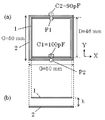
FIG. 1 (a) shows a plan view (XY diagram) of the transmitting antenna 1 and the receiving antenna 2 of the inductive power transmission circuit of the present invention, and FIG. 1 (b) shows a side view. That is, the inductive power transmission circuit of the present invention creates a resonance circuit in which both ends of the wiring of the coiled transmission antenna 1 having an effective self-inductance L1 are connected by the capacitor C1, and the port 1 in the middle of the antenna wiring of the resonance circuit. The power supply circuit 3 is connected in series with (P1). Similarly, a resonance circuit is formed by connecting both ends of the coiled receiving antenna 2 having effective self-inductance L2 with a capacitor C2, and a load circuit is connected in series with the port 2 (P2) in the middle of the antenna wiring of the resonance circuit. 4 is connected. As shown in FIG. 1, both antennas that electromagnetically induce each other are brought close to a distance of (wavelength of electromagnetic field at which the antenna resonates) / (2π) or less. By approaching this near distance, the interaction of electromagnetic induction that does not radiate radio waves becomes dominant in both antennas. Further, when the wiring of the transmitting antenna 1 and the wiring of the receiving antenna 2 are slightly separated, the mutual inductance M of the wirings of both antennas becomes 60% or less of the mutual inductance √ (L1 × L2) of the tightly coupled mutual induction circuit. .

図1では、送信アンテナ1のコイル状の配線が乗るアンテナの面(XY面)と受信アンテナ2のアンテナの面を平行にし、送信アンテナ1と受信アンテナ2のコイル状のアンテナの配線の中心軸を一致させて、アンテナ同士をその中心軸の方向に近づけて設置した。両アンテナの配置はこれに限らず、(アンテナが共振する電磁界の波長)/(2π)以下の距離の近傍に設置するだけで良く、後の図20(a)に示すように両アンテナを同一平面上に並べて配置しても良い。また、アンテナの形状は、アンテナの配線の両端を容量でつなぐだけで良く、アンテナの配線の巻数は1巻でも多数巻きのコイル状又は螺旋状でも良い。アンテナ配線の両端を結ぶ容量C1あるいはC2は、外付けコンデンサを接続しないでも、アンテナ配線の両端を開放して両端間に発生する寄生容量でアンテナ配線の両端をつなぐだけの構成でも良い。アンテナの形状及び寸法は送信アンテナ1と受信アンテナ2で異なっていても良い。更に、送信アンテナ1と受信アンテナ2は、図1のようなコイル状に形成しないで、例えば、図24(a)の送信アンテナ1のようにダイポールアンテナを共鳴させることでも電力を完全な効率(後に説明する式29で与えられる電力伝送効率Peで電力を伝送できることを完全な効率と呼ぶ)で伝送できる。   In FIG. 1, the antenna surface (XY plane) on which the coiled wiring of the transmitting antenna 1 rides and the antenna surface of the receiving antenna 2 are parallel, and the central axis of the coiled antenna wiring of the transmitting antenna 1 and the receiving antenna 2 The antennas were placed close to each other in the direction of the central axis. The arrangement of both antennas is not limited to this, and it is only necessary to install them in the vicinity of a distance of (the wavelength of the electromagnetic field at which the antenna resonates) / (2π) or less. As shown in FIG. They may be arranged side by side on the same plane. The antenna may be formed by simply connecting both ends of the antenna wiring with a capacitance, and the number of turns of the antenna wiring may be one or many coils or a spiral. The capacitor C1 or C2 connecting both ends of the antenna wiring may have a configuration in which both ends of the antenna wiring are connected by a parasitic capacitance generated between both ends by opening both ends of the antenna wiring without connecting an external capacitor. The shape and dimensions of the antenna may be different between the transmitting antenna 1 and the receiving antenna 2. Further, the transmitting antenna 1 and the receiving antenna 2 are not formed in a coil shape as shown in FIG. 1, and the power can be completely efficient (for example, by resonating the dipole antenna as in the transmitting antenna 1 in FIG. 24A). The fact that power can be transmitted with the power transmission efficiency Pe given by Equation 29 described later is referred to as perfect efficiency).

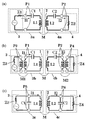
本発明の誘導電力伝送回路は、図2(a)の回路図でモデル化でき、その回路は、実効的自己インダクタンスL1の送信アンテナ1と実効的自己インダクタンスL2の受信アンテナ2が、相互インダクタンスMを持つ。そして、送信アンテナ1に接続した電源回路3から受信アンテナ2に接続した負荷回路4まで非接触で電力を供給する誘導電力伝送回路である。ここで、送信アンテナ1の両端をつなぐ容量C1は、電源回路3から角周波数ωの電流を送信アンテナ1に供給するタンク回路内に設置した容量で構成しても良い。また、寄生容量に比べて大きな容量C1をアンテナ配線の両端に接続した場合、送信アンテナ1に電源回路3を直列に接続する端子のポート1(P1)の位置は、容量C1と送信アンテナ1のアンテナ配線との接続部分に直列に挿入して設置しても良い。寄生容量に比べて大きな容量C2をアンテナ配線の両端に接続した場合、受信アンテナ2に負荷回路4を直列に接続する端子のポート2(P2)の位置も、容量C2と受信アンテナ2のアンテナ配線との接続部分に直列に挿入して設置しても良い。   The inductive power transmission circuit of the present invention can be modeled by the circuit diagram of FIG. 2A, and the circuit includes a transmission antenna 1 having an effective self-inductance L1 and a receiving antenna 2 having an effective self-inductance L2, and a mutual inductance M. have. The induction power transmission circuit supplies power in a non-contact manner from the power supply circuit 3 connected to the transmission antenna 1 to the load circuit 4 connected to the reception antenna 2. Here, the capacitor C <b> 1 that connects both ends of the transmission antenna 1 may be configured by a capacitor installed in a tank circuit that supplies current of the angular frequency ω from the power supply circuit 3 to the transmission antenna 1. Further, when a capacitance C1 larger than the parasitic capacitance is connected to both ends of the antenna wiring, the position of the port 1 (P1) of the terminal for connecting the power supply circuit 3 to the transmission antenna 1 in series is the position of the capacitance C1 and the transmission antenna 1. You may insert and install in series in the connection part with an antenna wiring. When a capacitance C2 larger than the parasitic capacitance is connected to both ends of the antenna wiring, the position of the port 2 (P2) of the terminal connecting the load circuit 4 to the receiving antenna 2 in series is also the antenna wiring of the capacitance C2 and the receiving antenna 2. It may be installed by inserting it in series with the connecting part.

鋭意研究の結果、以上の回路構成で誘導電力伝送回路を構成すると、送信アンテナ1と容量C1により共振回路を構成した送信回路3aと、受信アンテナ2と容量C2により共振回路を構成した受信回路4aを共鳴させることができ、以下の条件を満たせば、電源回路3から負荷回路4まで電力を完全な効率で伝送することができることを見出し、本発明に至った。電力を効率良く伝送する条件を以下で説明する。図2(a)の電源回路3を送信アンテナ回路1に接続するポート1(P1)の電圧Einは以下の式1であらわせる。
(式1)Ein=j{ωL1−(1/(ωC1))}×I1+jωM×I2
ここで、I1は送信アンテナ1に流れるアンテナ電流、I2は受信アンテナ2に流れるアンテナ電流であり、ω=2πfはその角周波数であり、fは高周波電流の周波数である。また、図2(a)の電源回路3側から見た、送信アンテナ回路1のポート1(P1)の入力インピーダンスZinに関しては、以下の式2が成り立つ
式2)Ein=Zin×I1
式1の右辺の最後の項のjωM×I2は、受信アンテナ2に流れる高周波のアンテナ電流I2が送信アンテナ1の配線の近傍の電磁界を時間変化させ、それが送信アンテナ1に誘導する誘導電圧E1である。それを式3であらわす。
(式3)E1=jωM×I2
式1と式2と式3から、アンテナ回路の入力インピーダンスZinが以下の式4であらわされる。
(式4)Zin=j{ωL1−(1/(ωC1))}+E1/I1
As a result of intensive research, when the inductive power transmission circuit is configured with the above circuit configuration, the transmission circuit 3a in which the resonance circuit is configured by the transmission antenna 1 and the capacitor C1, and the reception circuit 4a in which the resonance circuit is configured by the reception antenna 2 and the capacitance C2. It has been found that if the following conditions are satisfied, power can be transmitted from the power supply circuit 3 to the load circuit 4 with complete efficiency, and the present invention has been achieved. The conditions for efficiently transmitting power will be described below. The voltage Ein of the port 1 (P1) that connects the power supply circuit 3 of FIG. 2A to the transmitting antenna circuit 1 is expressed by the following equation 1.
(Equation 1) Ein = j {ωL1- (1 / (ωC1))} × I1 + jωM × I2
Here, I1 is the antenna current flowing through the transmitting antenna 1, I2 is the antenna current flowing through the receiving antenna 2, ω = 2πf is the angular frequency, and f is the frequency of the high-frequency current. Further, with respect to the input impedance Zin of the port 1 (P1) of the transmitting antenna circuit 1 as viewed from the power supply circuit 3 side in FIG .
( Formula 2) Ein = Zin × I1
JωM × I2 in the last term on the right side of Equation 1 is the induced voltage that the high-frequency antenna current I2 flowing in the receiving antenna 2 changes the electromagnetic field in the vicinity of the wiring of the transmitting antenna 1 over time, and that induces the transmitting antenna 1 E1. This is expressed by Equation 3.
(Formula 3) E1 = jωM × I2
From Equation 1, Equation 2, and Equation 3, the input impedance Zin of the antenna circuit is expressed by Equation 4 below.
(Formula 4) Zin = j {ωL1- (1 / (ωC1))} + E1 / I1

この入力インピーダンスZinは、誘導電圧E1に起因する見かけのインピーダンス(E1/I1)と回路のインピーダンスの和になる。そして、その加わったインピーダンス(E1/I1)の実数成分により、Zinは実数成分を持つ。そのZinの実数成分を誘導抵抗r1として、以下の式5であらわす。
(式5)r1≡Real(E1/I1)=Real(jωM×I2/I1)
ここで、受信アンテナ2の電流I2と送信アンテナ1の電流I1の比を、実数の電流比パラメータαと位相角βを用いて以下の式6であらわすと、誘導抵抗r1は式7であらわせる。
(式6)I2/I1≡α・exp(−jβ)
(式7)r1=α・ωM・sin(β)
ここで、電源回路3から最も効率良く送信アンテナ1に電力を供給する条件は、電源回路3のインピーダンスZ1が図2(a)の電源回路3側から送信アンテナ1のポート1(P1)を見た回路のインピーダンスZinと整合する(等しくなる)ことである。電源回路3の出力インピーダンスZ1が純抵抗の場合は、そのZ1が誘導抵抗r1に等しくなることが整合の条件であると考える。この誘導抵抗r1は、受信アンテナ2の電流I2が送信アンテナ1に誘導する電圧E1のうち送信アンテナ1の電流I1と同位相の成分を送信アンテナの電流I1で割り算した値である。
This input impedance Zin is the sum of the apparent impedance (E1 / I1) caused by the induced voltage E1 and the impedance of the circuit. And Zin has a real component by the real component of the added impedance (E1 / I1). The real number component of the Zin is expressed by the following formula 5 as an induction resistance r1.
(Formula 5) r1≡Real (E1 / I1) = Real (jωM × I2 / I1)
Here, when the ratio of the current I2 of the receiving antenna 2 and the current I1 of the transmitting antenna 1 is expressed by the following formula 6 using the real current ratio parameter α and the phase angle β, the induction resistance r1 is expressed by formula 7. .
(Formula 6) I2 / I1≡α · exp (−jβ)
(Expression 7) r1 = α · ωM · sin (β)
Here, the condition for supplying power from the power supply circuit 3 to the transmission antenna 1 most efficiently is that the impedance Z1 of the power supply circuit 3 looks at the port 1 (P1) of the transmission antenna 1 from the power supply circuit 3 side in FIG. It matches (becomes equal to) the impedance Zin of the circuit. When the output impedance Z1 of the power supply circuit 3 is a pure resistance, it is considered that the matching condition is that Z1 becomes equal to the induction resistance r1. The induction resistance r1 is a value obtained by dividing a component having the same phase as the current I1 of the transmission antenna 1 out of the voltage E1 induced by the current I2 of the reception antenna 2 by the transmission antenna 1 by the current I1 of the transmission antenna.

一方、受信アンテナ2にも送信アンテナ1のアンテナ電流I1で誘導される誘導電圧E2が発生する。その誘導電圧E2を式8であらわす。
(式8)E2=jωM×I1
すると、受信アンテナ2を負荷回路4に接続するポート2(P2)の電圧Eoutは以下の式9と式10であらわされる。
(式9)Eout=E2+j{ωL2−(1/(ωC2))}×I2
(式10)Eout=−Z2×I2
この誘導電圧E2の出力インピーダンスの実数成分を誘導抵抗r2とすると、誘導抵抗r2は以下の式11であらわされる。
(式11)r2≡Real(E2/(−I2))
=Real(−jωM×I1/I2)=(1/α)・ωM・sin(β)
ここで、受信アンテナ2から最も効率良く負荷回路4に電力を供給する条件は、受信アンテナ2に加わった誘導電圧E2を電源と見なして、その電源の出力インピーダンス(−E2/I2)が負荷回路4の入力インピーダンスZ2と受信アンテナの回路のリアクタンスj{ωL1−(1/(ωC1))}の和に整合する(等しくなる)ことであると考える。そのため、負荷回路4の入力インピーダンスZ2が純抵抗の場合は、そのZ2が誘導抵抗r2に等しくなることが整合の条件であると考える。この誘導抵抗r2は、送信アンテナ1の電流I1が受信アンテナ2に誘導する電圧E2のうち受信アンテナ2の電流I2と同位相の成分を受信アンテナの電流I2で割り算した値である。
On the other hand, an induction voltage E2 induced by the antenna current I1 of the transmission antenna 1 is also generated in the reception antenna 2. The induced voltage E2 is expressed by Equation 8.
(Formula 8) E2 = jωM × I1
Then, the voltage Eout of the port 2 (P2) connecting the receiving antenna 2 to the load circuit 4 is expressed by the following formulas 9 and 10.
(Equation 9) Eout = E2 + j {ωL2- (1 / (ωC2))} × I2
(Formula 10) Eout = −Z2 × I2
When the real component of the output impedance of the induction voltage E2 is an induction resistance r2, the induction resistance r2 is expressed by the following equation 11.
(Formula 11) r2≡Real (E2 / (− I2))
= Real (-jωM × I1 / I2) = (1 / α) · ωM · sin (β)
Here, the condition for supplying power from the receiving antenna 2 to the load circuit 4 most efficiently is that the induced voltage E2 applied to the receiving antenna 2 is regarded as a power source, and the output impedance (−E2 / I2) of the power source is the load circuit. 4 is matched (equalized) to the sum of the input impedance Z2 of 4 and the reactance j {ωL1- (1 / (ωC1))} of the circuit of the receiving antenna. Therefore, when the input impedance Z2 of the load circuit 4 is a pure resistance, it is considered that the matching condition is that the Z2 is equal to the induction resistance r2. This induction resistance r2 is a value obtained by dividing a component having the same phase as the current I2 of the receiving antenna 2 out of the voltage E2 that the current I1 of the transmitting antenna 1 induces to the receiving antenna 2 by the current I2 of the receiving antenna.

また、本発明は、図2(b)の右側の受信回路4bのように、受信アンテナ2に直列に変成器の一次巻線を接続し、その変成器の二次巻線の両端のポート4(P4)に負荷回路4を接続する受信回路を構成することもできる。図2(b)の右側の受信回路4bは、角周波数ωを1つに限定する条件下では、図2(a)の右側の受信回路4aに等価な回路であると考える。受信アンテナ2を図2(b)の右側の受信回路4bのように変成器により負荷回路4と接続する一実施形態として、図21(a)のように、受信アンテナ2のコイル状(螺旋状)の配線自体をその変成器の一次巻線とし、その受信アンテナ2のアンテナ面(XY面)に平行に近接したコイル状又は螺旋状の誘導結合配線6を変成器の二次巻線とする受信回路を構成することもできる。送信アンテナ1側の回路は、図2(a)の左側の送信回路3aのように、両端を容量C1に接続した送信アンテナ1の中間に電源回路3と直列に接続するポート1を設けた。図2(b)の右側の受信回路4bでは、受信アンテナ2に誘導結合配線6を相互インダクタンスM2で誘導結合させ、誘導結合配線6の両端をポート4(P4)として負荷回路4に接続する回路構成にする。図21(a)の場合においては、誘導結合配線6の有する自己インダクタンスが誘導抵抗r2に比べて小さいことにより、ポート4(P4)の負荷回路4側から見た誘導抵抗(誘導結合配線6のインピーダンス)が(2πf×M2)/r2になる。送信アンテナ1側も、図2(b)の左側の送信回路3bにし、その回路を誘導結合配線6を用いた回路構成にすることができる。 Further, according to the present invention, a primary winding of a transformer is connected in series to the receiving antenna 2 as in the receiving circuit 4b on the right side of FIG. 2B, and the ports 4 at both ends of the secondary winding of the transformer. A receiving circuit for connecting the load circuit 4 to (P4) can also be configured. The right receiving circuit 4b in FIG. 2B is considered to be an equivalent circuit to the right receiving circuit 4a in FIG. 2A under the condition that the angular frequency ω is limited to one. As an embodiment in which the receiving antenna 2 is connected to the load circuit 4 by a transformer like the receiving circuit 4b on the right side of FIG. 2B, a coil shape (spiral shape) of the receiving antenna 2 as shown in FIG. ) Is the primary winding of the transformer, and the coiled or spiral inductive coupling wiring 6 that is close to the antenna surface (XY plane) of the receiving antenna 2 is used as the secondary winding of the transformer. A receiving circuit can also be configured. The circuit on the side of the transmission antenna 1 is provided with a port 1 connected in series with the power supply circuit 3 in the middle of the transmission antenna 1 whose both ends are connected to the capacitor C1, like the transmission circuit 3a on the left side of FIG. In the receiving circuit 4b on the right side of FIG. 2B, the inductive coupling wiring 6 is inductively coupled to the receiving antenna 2 with the mutual inductance M2, and both ends of the inductive coupling wiring 6 are connected to the load circuit 4 as ports 4 (P4). Make the configuration. In the case of FIG. 21A, since the self-inductance of the inductive coupling wiring 6 is smaller than the inductive resistance r2, the inductive resistance (inductive coupling wiring 6 of the port 4 (P4)) is viewed from the load circuit 4 side. Impedance) becomes (2πf × M2) 2 / r2. The transmission antenna 1 side can also be a transmission circuit 3 b on the left side of FIG. 2B, and the circuit can be configured with an inductive coupling wiring 6.

また、図21(a)の受信アンテナ2と誘導結合配線6の回路は、更に、受信アンテナ2に誘導結合配線6を兼ねさせた回路にすることもできる。その場合は、図2(c)の右側の受信回路4cのように、誘導結合配線6の両端のポート4(P4)は受信アンテナ2のアンテナ配線の両端のポート6(P6)が兼ね、そのポート6(P6)に、負荷回路4を接続して受信回路4cを構成することができる。ポート6(P6)は容量C2に並列に設置され、ポート6の負荷回路4側から見た誘導抵抗(インピーダンス)が(ω・L2)/r2になる。すなわち、受信回路4cは、図2(b)の回路の誘導結合配線6の相互インダクタンスM2を、受信アンテナ2の実効的自己インダクタンスL2に置き換えた回路になる。送信アンテナ1側も、図2(b)の図の左の送信回路3bのように、誘導結合配線6のポート3(P3)に電源回路3を接続した回路構成にでき、また、図2(c)の送信回路3cのように、送信アンテナ1のポート5(P5)に電源回路3を接続した回路構成にすることができる。 Further, the circuit of the reception antenna 2 and the inductive coupling wiring 6 in FIG. 21A can be a circuit in which the reception antenna 2 also serves as the inductive coupling wiring 6. In that case, as in the receiving circuit 4c on the right side of FIG. 2C, the ports 4 (P4) at both ends of the inductive coupling wiring 6 also serve as the ports 6 (P6) at both ends of the antenna wiring of the receiving antenna 2, The receiving circuit 4c can be configured by connecting the load circuit 4 to the port 6 (P6). The port 6 (P6) is installed in parallel with the capacitor C2, and the inductive resistance (impedance) viewed from the load circuit 4 side of the port 6 is (ω · L2) 2 / r2. That is, the receiving circuit 4c is a circuit in which the mutual inductance M2 of the inductive coupling wiring 6 in the circuit of FIG. 2B is replaced with the effective self-inductance L2 of the receiving antenna 2. The transmission antenna 1 side can also have a circuit configuration in which the power supply circuit 3 is connected to the port 3 (P3) of the inductive coupling wiring 6 as shown in the left transmission circuit 3b of FIG. 2B. A circuit configuration in which the power supply circuit 3 is connected to the port 5 (P5) of the transmission antenna 1 can be provided as in the transmission circuit 3c of c).

また、図24(a)のように、受信アンテナ2は、コイル状(螺旋状)のアンテナ配線にし、一方、送信アンテナ1とそれに接続する電源回路3は、空間から電磁波を受け取るダイポールアンテナで両機能を兼用した誘導電力伝送回路を構成することもできる。その場合は、そのダイポールアンテナが、空間の電磁波から電力を受け取って電流を流し、その電流が受信アンテナ2に誘導電圧を発生する、電源回路3と送信アンテナ1の両機能を兼用する。この誘導電圧が受信アンテナ2に誘導抵抗r2を発生させ、その誘導抵抗r2に負荷回路4の入力インピーダンスZ2を等しくして空間の電磁波から効率良く電力を受け取ることができる。同様な回路として、送信アンテナ1は、コイル状(螺旋状)のアンテナ配線にし、一方、受信アンテナ2とそれに接続する負荷回路4は、空間に電磁波を放射するダイポールアンテナにし、空間へ電磁波を放射して電力を消費する負荷回路4と受信アンテナ2の機能をダイポールアンテナに兼用させた誘導電力伝送回路を構成することもできる。その場合は、負荷回路4の入力インピーダンスZ2となるダイポールアンテナの放射抵抗に、受信アンテナ2の誘導抵抗r2を整合させる(等しくする)ことで、空間に効率良く電磁波を放射することができる。   Further, as shown in FIG. 24A, the receiving antenna 2 is a coiled (spiral) antenna wiring, while the transmitting antenna 1 and the power supply circuit 3 connected thereto are dipole antennas that receive electromagnetic waves from space. An inductive power transmission circuit that also functions can be configured. In that case, the dipole antenna receives both electric power from the electromagnetic wave in the space and causes a current to flow. The current generates an induced voltage in the receiving antenna 2, and both functions of the power supply circuit 3 and the transmitting antenna 1 are combined. This induced voltage causes an induction resistor r2 to be generated in the receiving antenna 2, and the input impedance Z2 of the load circuit 4 is made equal to the induction resistor r2 so that power can be efficiently received from electromagnetic waves in the space. As a similar circuit, the transmitting antenna 1 is a coiled (spiral) antenna wiring, while the receiving antenna 2 and the load circuit 4 connected to the receiving antenna 2 are dipole antennas that radiate electromagnetic waves into the space, and radiate electromagnetic waves into the space. Thus, it is possible to configure an inductive power transmission circuit in which the functions of the load circuit 4 and the receiving antenna 2 that consume power are also used as a dipole antenna. In that case, by matching (equalizing) the induction resistance r2 of the receiving antenna 2 with the radiation resistance of the dipole antenna that becomes the input impedance Z2 of the load circuit 4, electromagnetic waves can be efficiently radiated into the space.

以下では、図2(a)の回路の誘導電力伝送回路でインピーダンスを整合させる場合に、共鳴をおこす角周波数ωがどうなるかを詳しく解析する。すなわち、電源回路3の出力インピーダンスZ1が誘導抵抗r1に等しい値に整合されて、負荷回路4の入力インピーダンスZ2が誘導抵抗r2に整合(等しく)される場合には、式1と式9等から、以下の式12と式13が成り立つ。
(式12)ωL1−(1/(ωC1))=−α・ωM・cos(β)
(式13)ωL2−(1/(ωC2))=−(1/α)・ωM・cos(β)
これらの式12と式13が成り立ちZ1=r1、Z2=r2の場合には、アンテナ1の電磁界とアンテナ2の電磁界が共鳴し、それにより、電源回路3から負荷回路4まで電力が完全な効率で伝送されると考える。
Hereinafter, in the case where impedance is matched in the inductive power transmission circuit of the circuit of FIG. 2A, what happens to the angular frequency ω causing resonance is analyzed in detail. That is, when the output impedance Z1 of the power supply circuit 3 is matched to a value equal to the induction resistance r1, and the input impedance Z2 of the load circuit 4 is matched (equal) to the induction resistance r2, The following expressions 12 and 13 hold.
(Formula 12) ωL1- (1 / (ωC1)) = − α · ωM · cos (β)
(Expression 13) ωL2- (1 / (ωC2)) = − (1 / α) · ωM · cos (β)
When these equations 12 and 13 hold and Z1 = r1 and Z2 = r2, the electromagnetic field of the antenna 1 and the electromagnetic field of the antenna 2 resonate, so that the power is completely transmitted from the power supply circuit 3 to the load circuit 4. Is considered to be transmitted with high efficiency.

ここで、cos(β)が0で無い場合には、式7、式11、式12、式13から以下の式が得られる。
(式14)r1・r2=(ωM)−g1×g2
(式15)g1≡ωL1−(1/(ωC1))
(式16)g2≡ωL2−(1/(ωC2))
(式17)α=g1/g2
(式18)sin(β)=Z1・Z2/(ωM)
MとL1とC1とL2とC2が定まっている場合は、式14により、ωに応じてr1・r2が求まり、そして式17から電流比パラメータαが求まる。次に、式18から、位相角βが求まる。次に、式7と式11によって、r1とr2が求まる。特に、式17から、g1×g2は正である。そして、ωMが小さい値の場合にも式14が成り立つには、ωがあるωoの場合にg1=g2=0になる必要がある。そのための条件は以下の式19である。
(式19)L1・C1=L2・C2≡(1/ωo)
Here, when cos (β) is not 0, the following expressions are obtained from Expression 7, Expression 11, Expression 12, and Expression 13.
(Formula 14) r1 · r2 = (ωM) 2 −g1 × g2
(Formula 15) g1≡ωL1- (1 / (ωC1))
(Expression 16) g2≡ωL2- (1 / (ωC2))
(Expression 17) α 2 = g1 / g2
(Formula 18) sin (β) 2 = Z1 · Z2 / (ωM) 2
When M, L1, C1, L2, and C2 are determined, r1 and r2 are obtained according to ω from Equation 14, and the current ratio parameter α is obtained from Equation 17. Next, from Expression 18, the phase angle β is obtained. Next, r1 and r2 are obtained by Expression 7 and Expression 11. In particular, from Equation 17, g1 × g2 is positive. In order for Equation 14 to hold even when ωM is a small value, it is necessary that g1 = g2 = 0 when ω is some ωo. The condition for this is Equation 19 below.
(Formula 19) L1 · C1 = L2 · C2≡ (1 / ωo) 2

(第1の共鳴の場合)
式19が成り立つ場合に、ω=ωoのとき、すなわち、式12及び式13でcos(β)が0でsin(β)が1になる場合に、g1=g2=0が成り立つ。この第1の共鳴の場合については後で説明する。
(第2の共鳴の場合)
式19が成り立つ場合に、ωがωo以外のときには、式6と式7と式11と式15から式17を使うと、以下の式20が成り立つ。これを第2の共鳴の場合と呼ぶ。
(式20)|I2/I1|=α=L1/L2=C2/C1=r1/r2
この式20から以下の式21が成り立つ。
(式21)L1×|I1|=L2×|I2|
この式21は、送信アンテナ1に蓄積される電磁界のエネルギーと受信アンテナ2に蓄積される電磁界のエネルギーが等しく、両アンテナが互いにその電磁界エネルギーを交換して共鳴している状態をあらわしていると考える。
この式21を変形して、以下の式22を得る。
(式22)|I2|=|I1|×√(L1/L2)
すなわち、共鳴した送信アンテナ1の電流I1と受信アンテナ2の電流I2の比が、受信アンテナ2の配線の実効的自己インダクタンスL2と送信アンテナ1の配線の実効的自己インダクタンスL1の比の平方根である。電磁界シミュレーションの結果でも、共振して効率良く(100%近い効率で)エネルギーを伝送するアンテナ回路では式22の関係が成り立っていた。式22のように受信アンテナ2に多くの電流が流れるので、受信アンテナ2に流れる高周波のアンテナ電流I2が電磁界を時間変化させ、それにより送信アンテナ1に誘導電圧E1を発生させると考える。
(In the case of the first resonance)
When Equation 19 holds, when ω = ωo, that is, when cos (β) is 0 and sin (β) is 1 in Equations 12 and 13, g1 = g2 = 0 holds. The case of this first resonance will be described later.
(In the case of the second resonance)
When Equation 19 is satisfied and ω is other than ωo, using Equation 6, Equation 7, Equation 11, and Equation 15 to Equation 17, the following Equation 20 is established. This is called the case of the second resonance.
(Expression 20) | I2 / I1 | 2 = α 2 = L1 / L2 = C2 / C1 = r1 / r2
From this equation 20, the following equation 21 holds.
(Formula 21) L1 × | I1 | 2 = L2 × | I2 | 2
This equation 21 represents a state in which the electromagnetic field energy stored in the transmitting antenna 1 and the electromagnetic field energy stored in the receiving antenna 2 are equal, and both antennas resonate with each other by exchanging their electromagnetic energy. I think.
This equation 21 is modified to obtain the following equation 22.
(Formula 22) | I2 | = | I1 | × √ (L1 / L2)
That is, the ratio of the resonant current I1 of the transmitting antenna 1 to the current I2 of the receiving antenna 2 is the square root of the ratio of the effective self inductance L2 of the wiring of the receiving antenna 2 to the effective self inductance L1 of the wiring of the transmitting antenna 1. . As a result of the electromagnetic field simulation, the relationship of Formula 22 is established in the antenna circuit that resonates and efficiently transmits energy (with an efficiency close to 100%). Since a large amount of current flows through the receiving antenna 2 as shown in Equation 22, it is considered that the high-frequency antenna current I2 flowing through the receiving antenna 2 changes the electromagnetic field over time, thereby generating an induced voltage E1 at the transmitting antenna 1.

ここで、式19が成り立つ場合は、送信アンテナ1と受信アンテナ2の電磁誘導の結合係数k(式23であらわす)を用いて、式7と式11と式12と式13が、式24から式27に書き換えられる。
(式23)k≡M/√(L1×L2)
(式24)r1=kωL1・sin(β)
(式25)r2=kωL2・sin(β)
(式26)ωL1−1/(ωC1)=−kωL1・cos(β)
(式27)ωL2−1/(ωC2)=−kωL2・cos(β)
式26と式27から、以下の式28が得られる。
(式28)ω=ωo/√(1+k・cos(β))
Here, when Expression 19 holds, Expression 7, Expression 11, Expression 12, and Expression 13 are obtained from Expression 24 using the electromagnetic induction coupling coefficient k (expressed by Expression 23) of the transmission antenna 1 and the reception antenna 2. Equation 27 is rewritten.
(Equation 23) k≡M / √ (L1 × L2)
(Equation 24) r1 = kωL1 · sin (β)
(Equation 25) r2 = kωL2 · sin (β)
(Equation 26) ωL1-1 / (ωC1) = − kωL1 · cos (β)
(Expression 27) ωL2-1 / (ωC2) = − kωL2 · cos (β)
From Expression 26 and Expression 27, the following Expression 28 is obtained.
(Formula 28) ω = ωo / √ (1 + k · cos (β))

以上の関係は、以下のように言い換えることができる。すなわち、L1×C1=L2×C2=1/ωoであるアンテナ系において、0からπラジアンまでの値の任意の位相角βに関して、電力を伝送する交流の角周波数ωを、L1×C1×(1+k・cos(β))の値の逆数の平方根にして、送信アンテナ1に直列にポート1(P1)で接続する電源回路3の出力インピーダンスZ1をr1=kωL1・sin(β)にし、受信アンテナに直列にポート2(P2)で接続する負荷回路4の入力インピーダンスZ2をr2=kωL2・sin(β)にすると、電力を完全な効率で伝送できる。そして、電源回路3から負荷回路4まで、電力を完全な効率で伝送できる誘導抵抗rの値に上限がある。空芯コイルの送信アンテナ1と受信アンテナ2を対向させ近づけると結合係数kが大きくなり電力を伝送できる誘導抵抗rの上限が大きくなる。誘導抵抗r1の上限がkωL1で、誘導抵抗r2の上限がkωL2であり、その上限以下の誘導抵抗r1に電源回路3の出力インピーダンスZ1を等しくし、誘導抵抗r2に負荷回路4の入力インピーダンスZ2を等しくすることで電力を完全な効率で伝送できる。電源回路3の出力インピーダンスZ1と負荷回路4の入力インピーダンスZ2を誘導抵抗rの上限より小さく設定する場合は、式24と式25でsin(β)が1より小さい値でそれらのインピーダンスが誘導抵抗に等しくなりインピーダンスが整合して電力が伝送できる。そして、その場合には、cos(β)が0では無く、式28により、ωoからずれた共振角周波数ωで送信アンテナ1と受信アンテナ2が共鳴する。 The above relationship can be paraphrased as follows. That is, in an antenna system in which L1 × C1 = L2 × C2 = 1 / ωo 2 , the angular frequency ω of the alternating current for transmitting power is expressed as L1 × C1 × for an arbitrary phase angle β having a value from 0 to π radians. Using the square root of the reciprocal of the value of (1 + k · cos (β)), the output impedance Z1 of the power supply circuit 3 connected in series to the transmitting antenna 1 via the port 1 (P1) is set to r1 = kωL1 · sin (β) When the input impedance Z2 of the load circuit 4 connected in series with the antenna at the port 2 (P2) is r2 = kωL2 · sin (β), power can be transmitted with complete efficiency. There is an upper limit to the value of the induction resistor r that can transmit power from the power supply circuit 3 to the load circuit 4 with complete efficiency. When the transmitting antenna 1 and the receiving antenna 2 of the air-core coil face each other and approach each other, the coupling coefficient k increases and the upper limit of the inductive resistance r that can transmit power increases. The upper limit of the induction resistance r1 is kωL1, the upper limit of the induction resistance r2 is kωL2, the output impedance Z1 of the power supply circuit 3 is made equal to the induction resistance r1 below the upper limit, and the input impedance Z2 of the load circuit 4 is set to the induction resistance r2. By making them equal, power can be transmitted with complete efficiency. When the output impedance Z1 of the power supply circuit 3 and the input impedance Z2 of the load circuit 4 are set to be smaller than the upper limit of the induction resistance r, the sin (β) is a value smaller than 1 in Expression 24 and Expression 25, and those impedances are the induction resistance. The impedance is matched and power can be transmitted. In this case, cos (β) is not 0, and the transmission antenna 1 and the reception antenna 2 resonate at a resonance angular frequency ω deviated from ωo according to Equation 28.

この第2の共鳴の場合の現象を利用して、送信アンテナ1と受信アンテナ2の位置が安定せず電磁誘導の結合係数kが変動する場合にも、誘導抵抗r1とr2に整合(等しい)する電源回路3と負荷回路4のインピーダンスを一定に保つことができる誘導電力伝送回路を構成できる。それは、上限の値より小さな値の誘導抵抗r1に等しい値の固定した値の出力インピーダンスZ1を有する電源回路3と、その際の誘導抵抗r2に等しい値の固定した値の入力インピーダンスZ2を有する負荷回路4を用い、結合係数kの値の変化に応じて位相角βを変え共振角周波数ωを変えるように電源回路3を適応させて共鳴させる。そのように適応する電源回路3の構成は、送信アンテナ1の共振電流を正帰還回路により電源回路3に正帰還させて、その電流を増幅して出力する電源回路3を構成することで実現できる。これにより、電源回路3から共振角周波数ωに適応した周波数の電流I1を取り出すことができ、電磁誘導の結合係数kの変化に適応してアンテナ回路を共鳴させ、結合係数kの変化があっても完全な効率の電力伝送を維持させる誘導電力伝送回路が構成できる効果がある。   By utilizing the phenomenon in the case of the second resonance, even when the positions of the transmitting antenna 1 and the receiving antenna 2 are not stable and the coupling coefficient k of electromagnetic induction varies, it is matched (equal) to the induction resistances r1 and r2. An inductive power transmission circuit that can keep the impedance of the power supply circuit 3 and the load circuit 4 constant can be configured. The power supply circuit 3 has a fixed output impedance Z1 having a value equal to the induction resistance r1 having a value smaller than the upper limit value, and a load having the fixed input impedance Z2 having a value equal to the induction resistance r2 at that time. Using the circuit 4, the power supply circuit 3 is adapted to resonate so as to change the phase angle β and change the resonance angular frequency ω in accordance with the change in the value of the coupling coefficient k. The configuration of the power supply circuit 3 that is adapted in this way can be realized by configuring the power supply circuit 3 that amplifies and outputs the current by positively feeding back the resonance current of the transmission antenna 1 to the power supply circuit 3 using a positive feedback circuit. . As a result, the current I1 having a frequency adapted to the resonance angular frequency ω can be extracted from the power supply circuit 3, and the antenna circuit is resonated in accordance with the change of the coupling coefficient k of electromagnetic induction, and the coupling coefficient k is changed. In addition, there is an effect that an inductive power transmission circuit capable of maintaining perfect power transmission can be configured.

ここで、アンテナ系の電力伝送効率Peは近似的に以下の式29で計算できると考える。
(式29)Pe=(1−ref2/r2)/(1+ref1/r1
ここで、ref1は送信アンテナ1の実効的抵抗、ref2は受信アンテナ2の実効的抵抗である。式29が有効になる条件は、誘導抵抗r2がref2より大きいことである。送信アンテナ1の実効的抵抗ref1が誘導抵抗r1に比べて小さく、受信アンテナ2の実効的抵抗ref2が誘導抵抗r2に比べて小さい場合に電力の伝送効率が良い。アンテナ配線の実効的抵抗refが誘導抵抗rに比べて無視できるほど小さい場合はほぼ100%の電力が伝送できると考える。また、送信アンテナ1と受信アンテナ2は、ダイポールアンテナに形成することもできるが、アンテナを図1のようなコイル状(渦巻き状)にアンテナ配線を巻くと、アンテナの実効的自己インダクタンスL1およびL2がダイポールアンテナの場合より大きくなり、式24と式25により誘導抵抗r1およびr2が大きくなるので、式29で計算される送信アンテナ1から受信アンテナ2までの電力伝送効率Peが大きくなる効果がある。
Here, it is considered that the power transmission efficiency Pe of the antenna system can be approximately calculated by the following equation 29.
(Formula 29) Pe = (1-ref2 / r2) / (1 + ref1 / r1 )
Here, ref1 is an effective resistance of the transmitting antenna 1, and ref2 is an effective resistance of the receiving antenna 2. The condition that Equation 29 becomes valid is that the induction resistance r2 is larger than ref2. When the effective resistance ref1 of the transmission antenna 1 is smaller than the induction resistance r1, and the effective resistance ref2 of the reception antenna 2 is smaller than the induction resistance r2, the power transmission efficiency is good . When the effective resistance ref of the antenna wiring is negligibly small compared to the induction resistance r, it is considered that almost 100% of power can be transmitted. The transmitting antenna 1 and the receiving antenna 2 can be formed as a dipole antenna. However, when the antenna wiring is wound in a coil shape (spiral shape) as shown in FIG. 1, effective self-inductances L1 and L2 of the antenna are obtained. Is larger than in the case of the dipole antenna, and the induction resistances r1 and r2 are increased according to Expression 24 and Expression 25. Therefore, there is an effect that the power transmission efficiency Pe from the transmission antenna 1 to the reception antenna 2 calculated by Expression 29 is increased. .

(第3の共鳴の場合)
特に、ω≒ωoの場合は、式26と式27の左辺が0に近くなるので、その右辺も0に近くなるため、βがπ/2ラジアンに近くなり、cos(β)が0に近くなり、sin(β)が1に近くなり、式24と式25は以下の式30と式31になる。
(式30)r1≒kωL1
(式31)r2≒kωL2
このように、ω≒ωoの場合に、図2(a)に示す電源回路3の出力インピーダンスZ1を式30の誘導抵抗r1に整合させ、負荷回路4の負荷インピーダンスZ2を式31の誘導抵抗r2に整合させると、電源回路3から負荷回路4まで、電力を完全な効率で伝送できる。この第3の共鳴の場合は、第2の共鳴の場合の一種であるだけで無く、第1の共鳴の場合の一種でもあり、第1の共鳴の場合と第2の共鳴の場合とが両立する場合である。また、第3の共鳴の場合には、誘導抵抗rと結合係数kとアンテナの実効的自己インダクタンスLの間に式30と式31の関係があるので、この関係を利用して、結合係数kが予め分かっている場合は、シミュレーションで求めた誘導抵抗rからアンテナの実効的自己インダクタンスLを求めることができる。また、実効的自己インダクタンスLが予め分かっている場合は、求めた誘導抵抗rから結合係数kを求めることができる。
(In the case of the third resonance)
In particular, in the case of ω≈ωo, the left side of Equation 26 and Equation 27 is close to 0, and the right side thereof is also close to 0. Therefore, β is close to π / 2 radians, and cos (β) is close to 0. Therefore, sin (β) is close to 1, and Expression 24 and Expression 25 become Expression 30 and Expression 31 below.
(Expression 30) r1≈kωL1
(Expression 31) r2≈kωL2
As described above, when ω≈ωo, the output impedance Z1 of the power supply circuit 3 shown in FIG. 2A is matched with the induction resistance r1 of Expression 30, and the load impedance Z2 of the load circuit 4 is changed to the induction resistance r2 of Expression 31. Therefore, power can be transmitted from the power supply circuit 3 to the load circuit 4 with complete efficiency. This third resonance is not only a type of the second resonance but also a type of the first resonance, and both the case of the first resonance and the case of the second resonance are compatible. This is the case. In the case of the third resonance, since there is a relationship of Equation 30 and Equation 31 among the inductive resistance r, the coupling coefficient k, and the effective self-inductance L of the antenna, the coupling coefficient k is utilized using this relationship. Is known in advance, the effective self-inductance L of the antenna can be obtained from the induction resistance r obtained by simulation. When the effective self-inductance L is known in advance, the coupling coefficient k can be obtained from the obtained induction resistance r.

(第1の共鳴の場合)
以下で、先に示した第1の共鳴の場合について詳しく説明する。第1の共鳴の場合は、式19が成り立つ場合に、sin(β)が1になる場合であって、g1=g2=0になる。この場合は、アンテナ電流I1とアンテナ電流I2の位相差をあらわす位相角βが90度(π/2ラジアン)の場合である。この場合は、角周波数ω=ωoで共振し、以下の式32から式35の状態でアンテナ系が共鳴する。
(式32)cos(β)=0
(式33)r1=ωM・α
(式34)r2=ωM/α
(式35)I2/I1=−jα
以上の関係は、以下のように言い換えることができる。すなわち、L1×C1=L2×C2=1/ωoであるアンテナ系において、電力を伝送する交流の角周波数ωをωoにし、任意の正の数αに関して、送信アンテナ1に直列に接続する電源回路3の出力インピーダンスZ1をr1=ωM・αにし、受信アンテナに直列に接続する負荷回路4の入力インピーダンスZ2をr2=ωM/αにすると、電力を完全な効率で伝送できる。つまり、この共鳴の場合は、式19で示すようにアンテナの共鳴の角周波数ω=2πfがωoに一致して共鳴するが、任意のアンテナ電流の比αで電力を伝送できる特徴がある。アンテナ電流の比αが任意であるという意味は、送信アンテナ1の電流I1を大きくして大きな電磁界を発生させれば、受信アンテナ2に流れる電流I2が小さくても良い効率で電力を伝送できることを意味する。逆に、受信アンテナ2に流れる電流I2が大きければ、送信アンテナ1の電流I1が小さくても良い効率で電力を伝送できることを意味する。なお、誘導抵抗r1とr2の積が(ωM)の二乗の一定値である。また、誘導抵抗r2に対するr1の比は、アンテナ電流の比αの二乗であって任意に変えることができる。
(In the case of the first resonance)
Hereinafter, the case of the first resonance described above will be described in detail. In the case of the first resonance, when Equation 19 holds, sin (β) is 1 and g1 = g2 = 0. In this case, the phase angle β representing the phase difference between the antenna current I1 and the antenna current I2 is 90 degrees ( π / 2 radians). In this case, the antenna system resonates at an angular frequency ω = ωo, and the antenna system resonates in the following equations 32 to 35.
(Formula 32) cos (β) = 0
(Expression 33) r1 = ωM · α
(Formula 34) r2 = ωM / α
(Formula 35) I2 / I1 = −jα
The above relationship can be paraphrased as follows. That is, in an antenna system in which L1 × C1 = L2 × C2 = 1 / ωo 2 , an AC angular frequency ω for transmitting power is set to ωo, and an arbitrary positive number α is connected to the transmission antenna 1 in series. When the output impedance Z1 of the circuit 3 is set to r1 = ωM · α, and the input impedance Z2 of the load circuit 4 connected in series to the receiving antenna is set to r2 = ωM / α, power can be transmitted with complete efficiency. That is, in the case of this resonance, the angular frequency ω = 2πf of resonance of the antenna resonates in accordance with ωo as shown in Equation 19 , but there is a feature that power can be transmitted with an arbitrary antenna current ratio α. The meaning that the ratio α of the antenna current is arbitrary means that if the current I1 of the transmitting antenna 1 is increased to generate a large electromagnetic field, power can be transmitted with an efficiency that allows the current I2 flowing through the receiving antenna 2 to be small. Means. Conversely, if the current I2 flowing through the receiving antenna 2 is large, it means that power can be transmitted with sufficient efficiency even if the current I1 of the transmitting antenna 1 is small. The product of the inductive resistances r1 and r2 is a constant value of the square of (ωM). The ratio of r1 to the induction resistance r2 is a square of the ratio α of the antenna current and can be arbitrarily changed.

この第1の共鳴の場合の現象を利用して、空芯コイルによる送信アンテナ1の誘導抵抗r1と受信アンテナ2の誘導抵抗r2を変換するインピーダンス変換回路を構成する誘導電力伝送回路が得られる。すなわち、図2(a)の回路で、電源回路3側のインピーダンスZ1を負荷回路4側の誘導抵抗r2=(ωM)/Z1に変換するインピーダンス変換回路を構成できる。また、このインピーダンス変換回路用の送信アンテナ1と受信アンテナ2の間隔を変えて結合係数kを変える、すなわち相互インダクタンスMを変えれば、送信アンテナ側の電源回路3の出力インピーダンスZ1を元のまま変えないで受信アンテナ2側の誘導抵抗r2の値だけを変えるインピーダンス変換回路を構成できる。このインピーダンス変換回路は、1つのパラメータkを変えるだけで変換結果の誘導抵抗r2の値を変えることができ、回路パラメータの調整が簡単であり容易にインピーダンスを調整できる効果がある。 By using the phenomenon in the case of the first resonance, an induction power transmission circuit constituting an impedance conversion circuit for converting the induction resistance r1 of the transmission antenna 1 and the induction resistance r2 of the reception antenna 2 by the air-core coil is obtained. That is, in the circuit of FIG. 2A, it is possible to configure an impedance conversion circuit that converts the impedance Z1 on the power supply circuit 3 side into the induction resistance r2 = (ωM) 2 / Z1 on the load circuit 4 side. If the coupling coefficient k is changed by changing the distance between the transmission antenna 1 and the reception antenna 2 for the impedance conversion circuit, that is, if the mutual inductance M is changed, the output impedance Z1 of the power supply circuit 3 on the transmission antenna side is changed as it is. Thus, an impedance conversion circuit that changes only the value of the induction resistor r2 on the receiving antenna 2 side can be configured. This impedance conversion circuit can change the value of the induction resistance r2 as a result of conversion only by changing one parameter k, and the adjustment of the circuit parameters is simple and the impedance can be easily adjusted.

以下では、各実施形態毎に、電磁界シミュレーションで、電源回路3から負荷回路4まで電力を完全な効率で伝送する電源回路3の出力インピーダンスZ1と負荷回路4の入力インピーダンスZ2を求め、その値を誘導抵抗r1とr2として誘導抵抗を求める。その誘導抵抗r1はωMα・sin(β)であって、誘導抵抗r2はωM・sin(β)/αである。以下に示す電磁界シミュレーションでは、送信アンテナ1と受信アンテナ2を空芯コイル状(螺旋状)に形成し、両アンテナの電磁誘導の結合係数kを0.01ぐらいに小さくするまで両アンテナを離して空間をあけた場合でも、両アンテナ回路を共鳴させることができた。そして、その共鳴させたアンテナ回路では、本発明の原理の第2の共鳴の場合には、インピーダンスZを式24と式25(式30と式31)であらわす誘導抵抗rに整合(等しく)させれば、電源回路3から負荷回路4へ電力を完全な伝送効率で伝送できる効果があることを見出した。また、本発明の原理の第1の共鳴の場合には、インピーダンスZを式33と式34であらわす誘導抵抗rに等しくすれば、電源回路3から負荷回路4へ電力を完全な伝送効率で伝送できる効果があることを見出した。なお、本発明は、共鳴させるアンテナ間の空間に真空や空気以外の、例えば誘電体媒質を充填した回路にも適用でき、また、常磁性体を充填した回路にも適用できる。また、本発明の誘導電力伝送回路は、電力をエネルギー供給のために伝送する用途だけに限定されず、信号伝達のために電力を送信アンテナ1から受信アンテナ2に伝送する用途の誘導電力伝送回路に用いることもできる。   In the following, for each embodiment, an electromagnetic field simulation determines the output impedance Z1 of the power supply circuit 3 and the input impedance Z2 of the load circuit 4 that transmit power from the power supply circuit 3 to the load circuit 4 with complete efficiency, and the values Is determined as induction resistances r1 and r2. The induction resistance r1 is ωMα · sin (β), and the induction resistance r2 is ωM · sin (β) / α. In the electromagnetic field simulation shown below, the transmitting antenna 1 and the receiving antenna 2 are formed in an air-core coil shape (spiral shape), and the antennas are separated until the electromagnetic induction coupling coefficient k of both antennas is reduced to about 0.01. Both antenna circuits were able to resonate even when the space was opened. In the resonant antenna circuit, in the case of the second resonance according to the principle of the present invention, the impedance Z is matched (equal) to the inductive resistance r expressed by Expression 24 and Expression 25 (Expression 30 and Expression 31). Then, it has been found that there is an effect that power can be transmitted from the power supply circuit 3 to the load circuit 4 with complete transmission efficiency. Further, in the case of the first resonance of the principle of the present invention, if the impedance Z is made equal to the induction resistance r expressed by the equations 33 and 34, the power is transmitted from the power supply circuit 3 to the load circuit 4 with perfect transmission efficiency. I found that there is an effect. The present invention can be applied to a circuit in which a space between antennas to be resonated is filled with, for example, a dielectric medium other than vacuum or air, and can also be applied to a circuit in which a paramagnetic material is filled. In addition, the inductive power transmission circuit of the present invention is not limited to the purpose of transmitting power for energy supply, but the inductive power transmission circuit for the purpose of transmitting power from the transmitting antenna 1 to the receiving antenna 2 for signal transmission. It can also be used.

<第1の実施形態>
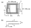
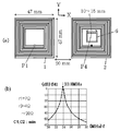
第1の実施形態は、生体内に受信アンテナを埋め込み、生体外に送信アンテナから皮膚を隔てて生体内の受信アンテナまで電力を伝送する誘導電力伝送回路を構成する。図1から図12により、第1の実施形態を説明する。図1では、送信アンテナ1は、平面上に形成した幅が1mmで厚さが50μmの銅のリボン状の配線でコイル径Dが46mmの1巻のコイルを形成した。その送信アンテナ1は例えば厚さ25μmのポリイミドフィルム上に形成する。また、受信アンテナ2は、コイル径Gが50mmのアンテナ配線を、厚さが25μmのポリイミド層で覆って作り、生体内に手術によって埋め込むことができる。その送信アンテナ1の配線の中間に電源回路3の端子のポート1(P1)を直列に接続して給電する。電源回路3から送信アンテナ1まで接続する給電線は電源回路3の出力インピーダンスZ1に整合する特性インピーダンスの給電線を用いる。例えば、電源回路3の出力インピーダンスZ1が4Ωの場合は、それに整合する給電線は、比誘電率が3.5のポリイミドの50μmの厚さのフィルムの両面に厚さが50μmで幅が2.4mmの銅の配線を対向させることで特性インピーダンスを4Ωにした給電線を用いる。送信アンテナ1には、その両端をつなぐ100pFの容量C1を設置した。配線パターンで形成する100pFの容量C1は、一辺の長さが34mmの正方形の電極を2つ平行に配置し0.1mmの空気の間隔をあけることで形成できる。また、厚さ0.025mmで誘電率が3.5のポリイミドの両面に46mm×1.8mmの矩形の電極を形成することでも100pFの容量を形成できる。受信アンテナ2は、幅が1mmで厚さが50μmの銅の配線でコイル径Gが50mmの1巻のコイルを厚さ0.025mmのポリイミドフィルムで覆って形成する。この受信アンテナ2の径は送信アンテナ1の径と異ならせた。その受信アンテナ2の配線の中間に負荷回路4の端子のポート2(P2)を直列に接続する。また、受信アンテナ2の両端をつなぐ90pFの容量C2を設置する。図1(b)の側面図のように、送信アンテナ1と受信アンテナ2は、アンテナのコイルの軸方向(XY面に垂直方向)にアンテナ間隔hの距離を隔てて配置する。そして、図2(a)の回路図の誘導電力伝送回路を構成し、電源回路3は、アンテナ回路が共鳴する角周波数ωの電流I1を送信アンテナ1に出力するように、出力電流I1を正帰還して増幅する電源回路に構成し、アンテナの共鳴角周波数ωで発振させる。
<First Embodiment>
The first embodiment configures an inductive power transmission circuit that embeds a receiving antenna in a living body and transmits power to the receiving antenna in the living body across the skin from the transmitting antenna outside the living body. The first embodiment will be described with reference to FIGS. In FIG. 1, the transmitting antenna 1 is formed by forming a single coil having a coil diameter D of 46 mm and a copper ribbon-like wiring having a width of 1 mm and a thickness of 50 μm formed on a plane. The transmitting antenna 1 is formed on a polyimide film having a thickness of 25 μm, for example. The receiving antenna 2 can be made by covering an antenna wiring having a coil diameter G of 50 mm with a polyimide layer having a thickness of 25 μm and implanting it in a living body by surgery. The port 1 (P1) of the terminal of the power supply circuit 3 is connected in series in the middle of the wiring of the transmitting antenna 1 to supply power. A power supply line connected from the power supply circuit 3 to the transmission antenna 1 uses a power supply line having a characteristic impedance that matches the output impedance Z1 of the power supply circuit 3. For example, when the output impedance Z1 of the power supply circuit 3 is 4Ω, the power supply line matched therewith has a thickness of 50 μm and a width of 2 μm on both surfaces of a polyimide film having a relative dielectric constant of 3.5 and a thickness of 50 μm. A feed line having a characteristic impedance of 4Ω by using a 4 mm copper wiring facing each other is used. The transmitting antenna 1 was provided with a capacitance C1 of 100 pF connecting both ends thereof. The capacitance C1 of 100 pF formed by the wiring pattern can be formed by arranging two square electrodes each having a length of 34 mm in parallel and leaving an air gap of 0.1 mm. A capacitance of 100 pF can also be formed by forming a rectangular electrode of 46 mm × 1.8 mm on both surfaces of polyimide having a thickness of 0.025 mm and a dielectric constant of 3.5. The receiving antenna 2 is formed by covering a single coil having a width of 1 mm and a thickness of 50 μm and a coil diameter G of 50 mm with a polyimide film having a thickness of 0.025 mm. The diameter of the receiving antenna 2 was different from the diameter of the transmitting antenna 1. The port 2 (P2) of the terminal of the load circuit 4 is connected in series in the middle of the wiring of the receiving antenna 2. In addition, a capacitance C2 of 90 pF that connects both ends of the receiving antenna 2 is installed. As shown in the side view of FIG. 1B, the transmitting antenna 1 and the receiving antenna 2 are arranged with an antenna interval h in the axial direction of the antenna coil (perpendicular to the XY plane). Then, the inductive power transmission circuit of the circuit diagram of FIG. 2A is configured, and the power supply circuit 3 positively outputs the output current I1 so as to output the current I1 of the angular frequency ω at which the antenna circuit resonates to the transmitting antenna 1. A power supply circuit that is fed back and amplified is configured to oscillate at the resonance angular frequency ω of the antenna.

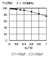
(電源回路3と負荷回路4のインピーダンスを整合させるアンテナの誘導抵抗値)
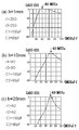
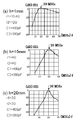
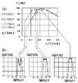
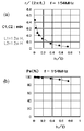
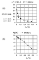
この誘導電力伝送回路の第3の共鳴の場合の電力伝送効率Peを電磁界シミュレーションで求め、その場合に発生する誘導抵抗r1とr2を以下のように求めた。すなわち、電源回路3から負荷回路4へ最も効率良く電力を伝送する電源回路3の出力インピーダンスZ1の値を求め、その値が送信アンテナ1の誘導抵抗r1であるとし、同じく、最も効率良く電力を伝送する場合の負荷回路4の負荷インピーダンスZ2の値が受信アンテナ2の誘導抵抗r2であるとする。図3に、アンテナ間隔hを種々に変えてシミュレーションした結果の、電源回路3から負荷回路4までの電力の伝送のSパラメータ(S21)をdB(デシベル)であらわして縦軸に示す。その横軸は、電源回路が送信アンテナ1に流すアンテナ電流I1の周波数fをあらわすグラフを示す。図3(a)は、図1のアンテナ間隔hが1mmの場合を示し、図3(b)はh=10mmの場合を示し、図3(c)は、h=20mmの場合を示す。図3(a)で、アンテナ間隔hが1mmの場合は、送信アンテナ1の誘導抵抗r1が20Ωであり、受信アンテナ2の誘導抵抗r2が23Ωである。この誘導抵抗rに電源回路3と負荷回路4のインピーダンスZを一致させた場合にアンテナが共鳴して電力の伝送効率が最も良くなり、アンテナ電流I1の周波数fが40MHzの場合の電力の伝送効率は100%に近かった。アンテナ間の距離は(アンテナが共振する電磁界の波長)/(2π)以下の近傍距離にする必要があるが、本実施形態では、周波数f=40MHzの電磁界の波長は約7.5mの波長であり、アンテナ間隔hを20mm離しても、そのアンテナ間隔hは(アンテナが共振する電磁界の波長)/(2π)の60分の1であり十分近い。図3(b)で、アンテナ間隔hが10mmの場合は、r1=8Ωでr2=9Ωであり、図3(c)で、アンテナ間隔hが20mmの場合は、r1=4Ωでr2=4Ωである。図3(c)の、アンテナ間隔hが20mmの場合でも、S21は−0.3dBであり92%の電力を伝送できた。
(Inductive resistance value of antenna for matching impedance of power supply circuit 3 and load circuit 4)
The power transmission efficiency Pe in the case of the third resonance of this induction power transmission circuit was obtained by electromagnetic field simulation, and the induction resistances r1 and r2 generated in that case were obtained as follows. That is, the value of the output impedance Z1 of the power supply circuit 3 that transmits the power most efficiently from the power supply circuit 3 to the load circuit 4 is obtained, and the value is the induction resistor r1 of the transmission antenna 1, and the power is also transmitted most efficiently. It is assumed that the value of the load impedance Z2 of the load circuit 4 when transmitting is the induction resistance r2 of the receiving antenna 2. FIG. 3 shows the S parameter (S21) of power transmission from the power supply circuit 3 to the load circuit 4 as a result of simulation by changing the antenna interval h in various ways in dB (decibel). The horizontal axis shows a graph representing the frequency f of the antenna current I1 that the power supply circuit passes through the transmitting antenna 1. 3A shows the case where the antenna interval h in FIG. 1 is 1 mm, FIG. 3B shows the case where h = 10 mm, and FIG. 3C shows the case where h = 20 mm. In FIG. 3A, when the antenna interval h is 1 mm, the induction resistance r1 of the transmission antenna 1 is 20Ω, and the induction resistance r2 of the reception antenna 2 is 23Ω. When the impedance Z of the power supply circuit 3 and the load circuit 4 is made to coincide with the induction resistor r, the antenna resonates and the power transmission efficiency becomes the best, and the power transmission efficiency when the frequency f of the antenna current I1 is 40 MHz. Was close to 100%. The distance between the antennas needs to be close to (the wavelength of the electromagnetic field at which the antenna resonates) / (2π) or less, but in this embodiment, the wavelength of the electromagnetic field having the frequency f = 40 MHz is about 7.5 m. Even if the antenna interval h is separated by 20 mm, the antenna interval h is 1/60 of (the wavelength of the electromagnetic field at which the antenna resonates) / (2π), which is sufficiently close. 3B, when the antenna interval h is 10 mm, r1 = 8Ω and r2 = 9Ω. In FIG. 3C, when the antenna interval h is 20 mm, r1 = 4Ω and r2 = 4Ω. is there. Even in the case where the antenna interval h in FIG. 3C is 20 mm, S21 was −0.3 dB, and 92% of power could be transmitted.

以上の場合は、アンテナ間隔hが1mm、10mm、20mmの場合とも、ほとんど100%の電力を伝送した。電力伝送効率が100%となる周波数fには周波数帯域(共鳴周波数帯域)の帯域幅があり、それは、図3(a)の、アンテナ間隔hが1mmの場合は、35MHzから55MHzまでの周波数帯域であり、約20MHzの周波数帯域幅がある。電力伝送効率がほぼ100%となる共鳴周波数帯域は、アンテナ間隔hが大きくなるにつれて狭まり、図3(b)の、アンテナ間隔hが10mmの場合は、共鳴周波数帯域は36MHzから46MHzまでの約8MHzの周波数帯域幅になる。図3(c)の、アンテナ間隔hが20mmの場合は、共鳴周波数帯域は38MHzから41MHzまでの約3MHzの周波数帯域幅になる。   In the above case, almost 100% of power was transmitted even when the antenna interval h was 1 mm, 10 mm, and 20 mm. The frequency f at which the power transmission efficiency is 100% has a frequency band (resonance frequency band), which is a frequency band from 35 MHz to 55 MHz when the antenna interval h is 1 mm in FIG. And has a frequency bandwidth of about 20 MHz. The resonance frequency band in which the power transmission efficiency is almost 100% narrows as the antenna interval h increases. When the antenna interval h is 10 mm in FIG. 3B, the resonance frequency band is about 8 MHz from 36 MHz to 46 MHz. Frequency bandwidth. When the antenna interval h in FIG. 3C is 20 mm, the resonance frequency band is a frequency bandwidth of about 3 MHz from 38 MHz to 41 MHz.

図3のシミュレーションの結果の共振周波数fが40MHzであり、送信アンテナ1の両端をつないだ容量C1が100pFであることから、送信アンテナ1の実効的自己インダクタンスL1が計算でき、L1は160nHである。また、受信アンテナ2の両端をつないだ容量C2が90pFであることから、受信アンテナ2の実効的自己インダクタンスL2は180nHである。これらのアンテナの両端を結ぶ容量Cの大きさがこれ以上ある場合は、アンテナの配線に流れる電流の大きさの分布は、アンテナの端部に至るまで同じ値でありアンテナの場所によらず一様であると考えられる。そのため、アンテナの実効的自己インダクタンスLは、それらの容量Cがこれ以上の大きさの場合には、同じ値になると考える。   Since the resonance frequency f of the simulation result of FIG. 3 is 40 MHz and the capacitance C1 connecting both ends of the transmission antenna 1 is 100 pF, the effective self-inductance L1 of the transmission antenna 1 can be calculated, and L1 is 160 nH. . Further, since the capacitance C2 connecting both ends of the receiving antenna 2 is 90 pF, the effective self-inductance L2 of the receiving antenna 2 is 180 nH. When the capacitance C connecting both ends of these antennas is larger than this, the distribution of the magnitude of the current flowing through the antenna wiring is the same value up to the end of the antenna, and is uniform regardless of the antenna location. It is thought that it is like. Therefore, the effective self-inductance L of the antenna is considered to be the same value when the capacitance C is larger than this.

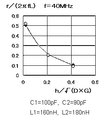
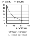
図4のグラフは、縦軸にシミュレーションで得た誘導抵抗r1を(2πfL1)で割り算して無次元量にした値r1/(2πfL1)を黒丸印で示し、r2を(2πfL2)で割り算して無次元量にした値r2/(2πfL2)を白丸印で示す。図4のグラフの横軸は、アンテナ間隔hを、コイル径Dとコイル径Gの積の平方根で割り算して無次元量にした(h/√(D×G))をあらわす。図4のグラフで、実線は、以下の近似式36で計算した結果を示す。
(式36)
r/(2πfL)=1.8EXP(−4.3√(0.04+√(1/t−1)))
(式37)
t=√(D×G/(((D+G)/2)+h))
近似式36のtは式37で計算される値である。図4で、実線で示す近似式36は、シミュレーション結果と良く一致する。
In the graph of FIG. 4, the value r1 / (2πfL1) obtained by dividing the induction resistance r1 obtained by the simulation by (2πfL1) to a dimensionless amount is indicated by a black circle on the vertical axis, and r2 is divided by (2πfL2). The dimensionless value r2 / (2πfL2) is indicated by a white circle. The horizontal axis of the graph in FIG. 4 represents the antenna interval h divided by the square root of the product of the coil diameter D and the coil diameter G to obtain a dimensionless amount (h / √ (D × G)). In the graph of FIG. 4, the solid line indicates the result calculated by the following approximate expression 36.
(Formula 36)
r / (2πfL) = 1.8EXP (−4.3√ (0.04 + √ (1 / t 2 −1)))
(Formula 37)
t = √ (D × G / (((D + G) / 2) 2 + h 2 ))
T in the approximate expression 36 is a value calculated by the expression 37. In FIG. 4, the approximate expression 36 indicated by the solid line is in good agreement with the simulation result.

図4の縦軸の値は、式30と式31と同じであるから、送信アンテナ1と受信アンテナ2の電磁誘導の結合係数kをあらわすことになる。それを確認するため、送信アンテナ1が直径Dの円形コイルで受信アンテナ2が直径Gの円形コイルの場合の、両コイル間の電磁誘導の結合係数kを理論的に厳密に計算し、以下の式39の係数Aであらわす式38を得た。
(式38)
k=A×((−t+2/t)×K(t)−(2/t)×E(t))
(式39)
A=μ√(D×G/(L1×L2))/2
ここで、μは透磁率であり、tは式37で定義し、K(t)は第1種完全楕円積分関数、E(t)は第2種完全楕円積分関数である。
Since the values on the vertical axis in FIG. 4 are the same as those in Expression 30 and Expression 31, the electromagnetic induction coupling coefficient k between the transmission antenna 1 and the reception antenna 2 is represented. In order to confirm this, when the transmitting antenna 1 is a circular coil with a diameter D and the receiving antenna 2 is a circular coil with a diameter G, the coupling coefficient k of electromagnetic induction between the two coils is theoretically strictly calculated. Equation 38 expressed by the coefficient A in Equation 39 was obtained.
(Formula 38)
k = A × ((− t + 2 / t) × K (t) − (2 / t) × E (t))
(Formula 39)
A = μ√ (D × G / (L1 × L2)) / 2
Here, μ is the magnetic permeability, t is defined by Equation 37, K (t) is the first type complete elliptic integral function, and E (t) is the second type complete elliptic integral function.

この式から以下の近似式40が得られる。
(式40)
k=4.86A{1.8EXP(−4.3√(0.04+√(1/t−1)))}
式40の最初の係数の4.86AにL1=160nHとL2=180nHと真空の透磁率μ=1.26μΩ・s/mを代入すると、それは約0.88で1割強程度の誤差で1になる。すなわち、式40で計算される両コイル間の電磁誘導の結合係数kは、1割強の誤差で近似式36の値に一致する。そのため、図4の縦軸は送信アンテナ1と受信アンテナ2の電磁誘導の結合係数kに一致すると言える。また、図4のグラフで、実線は、近似式36で計算した結果であり、それは、ほぼ両アンテナの配線の電磁誘導の結合係数kの計算結果をあらわしている。図4において、近似式36で計算した結合係数kとシミュレーション結果のr/(2πfL)は良く一致した。そのため、シミュレーション結果は式30と式31の計算結果に一致すると言える。
From this equation, the following approximate equation 40 is obtained.
(Formula 40)
k = 4.86A {1.8 EXP (−4.3√ (0.04 + √ (1 / t 2 −1)))}
Substituting L1 = 160 nH, L2 = 180 nH, and vacuum permeability μ = 1.26 μΩ · s / m into the initial coefficient of 4.86 A in Equation 40, it is about 0.88, which is an error of about 10%. become. That is, the coupling coefficient k of the electromagnetic induction between both coils calculated by Expression 40 matches the value of the approximate expression 36 with an error of more than 10%. Therefore, it can be said that the vertical axis in FIG. 4 matches the electromagnetic induction coupling coefficient k of the transmission antenna 1 and the reception antenna 2. Further, in the graph of FIG. 4, the solid line is the result calculated by the approximate expression 36, which almost represents the calculation result of the electromagnetic induction coupling coefficient k of the wirings of both antennas. In FIG. 4, the coupling coefficient k calculated by the approximate expression 36 and r / (2πfL) of the simulation result are in good agreement. Therefore, it can be said that the simulation result agrees with the calculation results of Expression 30 and Expression 31.

(電力伝送効率を飽和させる周波数の帯域幅)
図4から、h=1mmで(h/√(D×G))が0.02の場合は、結合係数kが0.5であり誘導抵抗rが約20Ωであり、h=10mmで(h/√(D×G))が0.2の場合は結合係数kが0.2であり誘導抵抗rが8Ωであり、h=20mmで(h/√(D×G))が0.4の場合は結合係数kが0.1であり誘導抵抗rが4Ωである。図3(a)のグラフは、h=1mmで結合係数k=0.5であり誘導抵抗rが約20Ωの場合の電力の伝送効率Peの周波数特性をSパラメータS21で示す。図3(b)のグラフは、h=10mmで結合係数k=0.2で誘導抵抗rが8Ωの場合を示し、図3(c)のグラフは、h=20mmで結合係数k=0.1で誘導抵抗rが4Ωの場合を示す。図3のこれらのグラフでは、電力の伝送効率Peが飽和する周波数fの帯域の上限は、ほぼf/fo=1/√(1−k)であり、下限は、ほぼf/fo=1/√(1+k)になっている。このため、結合係数kを大きくすると、電力の伝送効率Peが飽和する周波数fの帯域幅の割合f/foが結合係数k程度の幅を確保できる効果がある。それゆえ、結合係数kを大きくすると、送信アンテナ1から受信アンテナ2への電力伝送効率Peを飽和させる周波数帯域幅を大きくでき、両アンテナの共振周波数同士を緩い精度で一致させれば十分であり、両アンテナ回路の製造と調整が容易になる効果がある。
(Frequency bandwidth that saturates power transmission efficiency)
From FIG. 4, when h = 1 mm and (h / √ (D × G)) is 0.02, the coupling coefficient k is 0.5, the induction resistance r is about 20Ω, and h = 10 mm (h / √ (D × G)) is 0.2, the coupling coefficient k is 0.2, the induction resistance r is 8Ω, h = 20 mm, and (h / √ (D × G)) is 0.4. In this case, the coupling coefficient k is 0.1 and the induction resistance r is 4Ω. In the graph of FIG. 3A, the frequency characteristic of the power transmission efficiency Pe when h = 1 mm, the coupling coefficient k = 0.5, and the inductive resistance r is about 20Ω is indicated by the S parameter S21. The graph of FIG. 3B shows a case where h = 10 mm, the coupling coefficient k = 0.2, and the induction resistance r is 8Ω, and the graph of FIG. 3C is a graph where h = 20 mm and the coupling coefficient k = 0. 1 and the induction resistance r is 4Ω. In these graphs of FIG. 3, the upper limit of the band of the frequency f at which the power transmission efficiency Pe is saturated is approximately f / fo = 1 / √ (1-k), and the lower limit is approximately f / fo = 1 / k. √ (1 + k). For this reason, when the coupling coefficient k is increased, there is an effect that the bandwidth ratio f / fo of the frequency f at which the power transmission efficiency Pe is saturated can secure a width of about the coupling coefficient k. Therefore, if the coupling coefficient k is increased, the frequency bandwidth for saturating the power transmission efficiency Pe from the transmitting antenna 1 to the receiving antenna 2 can be increased, and it is sufficient to match the resonance frequencies of both antennas with a low degree of accuracy. This has the effect of facilitating the manufacture and adjustment of both antenna circuits.

本実施形態で、電力の伝送効率Peが飽和する周波数fの帯域幅の割合f/foが結合係数k程度の幅を確保できるので、誘導電力伝送回路の送信アンテナ1と受信アンテナ2の結合係数kを0.004以上に設定して電力を伝送すると、周波数fの帯域幅が共振周波数の0.4%以上の幅を確保することができる。そのため、結合係数kを0.004以上にすることが望ましい。そうすれば、誘導電力伝送回路に用いる部品の特性のバラツキを0.4%以内にして送信アンテナ1と受信アンテナ2の共振周波数のバラツキを0.4%以内にすることが比較的容易にできるので、この両アンテナの共振周波数のずれは電力を伝送するのに支障が無い程度の範囲内に収めることができる効果が得られる。   In this embodiment, since the bandwidth ratio f / fo at which the power transmission efficiency Pe saturates can secure a width of about the coupling coefficient k, the coupling coefficient between the transmission antenna 1 and the reception antenna 2 of the inductive power transmission circuit. When power is transmitted with k set to 0.004 or more, the bandwidth of the frequency f can be ensured to be 0.4% or more of the resonance frequency. For this reason, it is desirable that the coupling coefficient k is 0.004 or more. By doing so, it is relatively easy to make the variation in the characteristics of the components used in the inductive power transmission circuit within 0.4% and the variation in the resonance frequency between the transmitting antenna 1 and the receiving antenna 2 within 0.4%. Therefore, it is possible to obtain an effect that the difference between the resonance frequencies of the two antennas can be kept within a range that does not hinder the transmission of power.

このように、本実施形態では、生体外の送信アンテナ1から生体内の受信アンテナ2に、周波数f=40MHzの高周波で電力を伝送し、電源回路3と負荷回路4のインピーダンスZ1とZ2を20Ωから4Ωの誘導抵抗r1とr2に整合することで電力を効率良く伝送できる効果がある。この効果は、アンテナ間の距離を(アンテナが共振する電磁界の波長)/(2π)以下の近傍にすることで得られる。本実施形態の誘導電力伝送回路は、電力を伝送するために誘導抵抗rに整合する電源回路3の出力インピーダンスZ1及び負荷回路4の入力インピーダンスZ2は、20Ωから4Ωで小さいため、所定の電力を伝送するための回路の電圧を低くでき、電力伝送回路の安全性が高い効果がある。本実施形態では、生体の外から、非接触で20mmの厚さの生体組織を隔てた生体内にも92%の効率で電力を伝送できる効果がある。また、生体内に埋め込む受信アンテナ2には、縦横50mmで幅が1mmで厚さが50μmの銅の配線を25μmの厚さの絶縁体で覆った薄いアンテナを用いることができ、生体内でアンテナが占有する体積が小さいので、生体内へ埋め込み易い効果がある。   As described above, in this embodiment, power is transmitted from the transmitting antenna 1 outside the living body to the receiving antenna 2 inside the living body at a high frequency of frequency f = 40 MHz, and the impedances Z1 and Z2 of the power supply circuit 3 and the load circuit 4 are 20Ω. Therefore, there is an effect that power can be efficiently transmitted by matching with the induction resistances r1 and r2 of 4Ω. This effect can be obtained by setting the distance between the antennas to be in the vicinity of (the wavelength of the electromagnetic field at which the antenna resonates) / (2π) or less. In the inductive power transmission circuit of the present embodiment, the output impedance Z1 of the power supply circuit 3 and the input impedance Z2 of the load circuit 4 matched to the inductive resistor r to transmit power are as small as 20Ω to 4Ω. The voltage of the circuit for transmission can be lowered, and the power transmission circuit is highly safe. In the present embodiment, there is an effect that power can be transmitted with an efficiency of 92% from outside the living body to a living body that is separated from a living tissue having a thickness of 20 mm without contact. In addition, as the receiving antenna 2 embedded in the living body, a thin antenna in which copper wiring having a length and width of 50 mm, a width of 1 mm, and a thickness of 50 μm is covered with an insulator having a thickness of 25 μm can be used. Since the volume occupied by is small, there is an effect that it can be easily implanted into a living body.

(変形例1)
変形例1は、生体内に埋め込んだ受信アンテナ2に電力を供給する交流の角周波数ωを低下させる誘導電力伝送回路を構成する。変形例1では、第1の実施形態の送信アンテナ1と受信アンテナ2の端部間容量C1とC2を、ほぼ4倍の、C1=400pFと、C2=360pFにする。図5のグラフに、縦軸にシミュレーション結果の電力の伝送のSパラメータ(S21)を、横軸を周波数fで表す。図5のグラフでは、電力を伝送する共振周波数fが第1の実施形態の半分の20MHzになった。図6に、縦軸に、変形例1における誘導抵抗rを無次元量のr/(2πfL)、すなわち結合係数kであらわし、横軸をアンテナ間隔hを無次元量の(h/√(D×G))であらわすグラフを示す。図6も、図4と同様に、黒丸印と白丸印はシミュレーション結果を示し、実線は、近似式36の計算値を示す。図6でも、シミュレーション結果は近似式36の計算結果と良く一致した。図6で、h=1mmで(h/√(D×G))が0.02の場合は、結合係数kが0.5であり誘導抵抗rが約10Ωであり、h=10mmで(h/√(D×G))が0.2の場合は結合係数kが0.2であり誘導抵抗rが4Ωであり、h=20mmで(h/√(D×G))が0.4の場合は結合係数kが0.1であり誘導抵抗rが2Ωであり、共振周波数fが半分になることで誘導抵抗rが半分になった。
(Modification 1)
The first modification constitutes an inductive power transmission circuit that lowers the angular frequency ω of alternating current that supplies power to the receiving
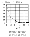
 antenna 2 embedded in the living body. In the first modification, the end-to-end capacitances C1 and C2 of the transmission antenna 1 and the reception antenna 2 of the first embodiment are approximately four times C1 = 400 pF and C2 = 360 pF. In the graph of FIG. 5, the vertical axis represents the S parameter (S21) of power transmission as a simulation result, and the horizontal axis represents the frequency f. In the graph of FIG. 5, the resonance frequency f for transmitting electric power is 20 MHz, which is half of the first embodiment. In FIG. 6, the vertical axis represents the inductive resistance r in Modification 1 as a dimensionless amount r / (2πfL), that is, the coupling coefficient k, and the horizontal axis represents the antenna interval h as a dimensionless amount (h / √ (D XG)) represents a graph. In FIG. 6, as in FIG. 4, black circles and white circles indicate simulation results, and a solid line indicates the calculated value of the approximate expression 36. Also in FIG. 6, the simulation result agrees well with the calculation result of the approximate expression 36. In FIG. 6, when h = 1 mm and (h / √ (D × G)) is 0.02, the coupling coefficient k is 0.5, the induction resistance r is about 10Ω, and h = 10 mm (h / √ (D × G)) is 0.2, the coupling coefficient k is 0.2, the induction resistance r is 4Ω, and h = 20 mm and (h / √ (D × G)) is 0.4. In this case, the coupling coefficient k is 0.1, the induction resistance r is 2Ω, and the induction resistance r is halved when the resonance frequency f is halved.

(変形例2)
変形例2は、家屋の壁を隔てて電力を伝送する誘導電力伝送回路を構成する。図7のように送信アンテナ1と受信アンテナ2を、それぞれ厚さが50μmのポリイミド膜の上に形成し、縦横の直径Dをともに50mmの同じ寸法のアンテナにした。アンテナの配線は、幅が1mmで厚さが50μmの銅の配線にし、アンテナの両端間の容量C1とC2をともに100pFにする。アンテナの配線の上は厚さが30μm程度のソルダーレジストを印刷するかポリイミド膜を被せる等で形成した絶縁膜で覆う。この場合において、送信アンテナ1に対して受信アンテナ2を水平面(XY面)の方向で縦(Y方向)と横(X方向)にずらすずれ距離dは0にした場合をシミュレーションした。その結果、アンテナ電流が37.4MHzの周波数fで共振することを確認し、アンテナの実効的自己インダクタンスはL1=L2=L=176nHであることがわかった。図8に、縦軸に誘導抵抗rを無次元量のr/(2πfL)=結合係数kであらわし、横軸にアンテナ間隔hを無次元量の(h/D)であらわすグラフを示す。図8のグラフの横軸は、アンテナの軸方向のアンテナ間隔hを2mmから50mmまで種々に変えた場合をあらわす。図8のグラフの黒丸印はシミュレーションから得たrをあらわし、実線は、近似式36の計算結果を示す。シミュレーション結果は近似式36と良く一致した。
(Modification 2)
The modification 2 comprises the inductive power transmission circuit which transmits electric power across the wall of a house. As shown in FIG. 7, the transmitting antenna 1 and the receiving antenna 2 were formed on a polyimide film having a thickness of 50 μm, respectively, and the vertical and horizontal diameters D were both 50 mm. The antenna wiring is a copper wiring having a width of 1 mm and a thickness of 50 μm, and the capacitances C1 and C2 between both ends of the antenna are both 100 pF. The antenna wiring is covered with an insulating film formed by printing a solder resist having a thickness of about 30 μm or covering with a polyimide film. In this case, a simulation was performed in which the shift distance d for shifting the reception antenna 2 with respect to the transmission antenna 1 in the horizontal (XY plane) direction in the vertical (Y direction) and horizontal (X direction) was set to zero. As a result, it was confirmed that the antenna current resonated at a frequency f of 37.4 MHz, and the effective self-inductance of the antenna was found to be L1 = L2 = L = 176 nH. FIG. 8 is a graph in which the vertical axis represents the inductive resistance r as a dimensionless amount r / (2πfL) = coupling coefficient k, and the horizontal axis represents the antenna interval h as a dimensionless amount (h / D). The horizontal axis of the graph of FIG. 8 represents the case where the antenna interval h in the axial direction of the antenna is variously changed from 2 mm to 50 mm. The black circles in the graph of FIG. 8 indicate r obtained from the simulation, and the solid line indicates the calculation result of the approximate expression 36. The simulation result agreed well with the approximate expression 36.

また、図8で、(h/D)が1の場合に誘導抵抗rが0.8Ωになり結合係数kが約0.02になった。また、(h/D)が2になる場合は、シミュレーションの結果の誘導抵抗rは0.24Ωになり、結合係数kは0.006になった。そして電力伝送効率Peは22%あった。結合係数kが0.006程度あれば、電力の伝送効率Peが飽和する周波数fの帯域幅の割合f/foは結合係数k程度の幅を確保できるため、電力伝送効率Peの飽和する周波数fの帯域幅は共振周波数foの0.6%程度ある。そのため、0.6%程度の特性のバラツキのある部品を使っても、送信アンテナ1と受信アンテナ2の共振周波数のバラツキを許容範囲内に留めることができる効果がある。このように、直径Dのコイルの送信アンテナ1と受信アンテナ2の間隔hをアンテナのコイルの直径Dの2倍以下にすることで、実用的な誘導電力伝送回路が構成できる効果がある。   In FIG. 8, when (h / D) is 1, the induction resistance r is 0.8Ω, and the coupling coefficient k is about 0.02. When (h / D) is 2, the inductive resistance r as a result of the simulation is 0.24Ω, and the coupling coefficient k is 0.006. The power transmission efficiency Pe was 22%. If the coupling coefficient k is about 0.006, the bandwidth ratio f / fo of the frequency f at which the power transmission efficiency Pe is saturated can secure a width of about the coupling coefficient k. Therefore, the frequency f at which the power transmission efficiency Pe is saturated. Is about 0.6% of the resonance frequency fo. For this reason, even if a component having a characteristic variation of about 0.6% is used, there is an effect that the variation in the resonance frequency of the transmitting antenna 1 and the receiving antenna 2 can be kept within an allowable range. Thus, by setting the distance h between the transmitting antenna 1 and the receiving antenna 2 of the coil having a diameter D to be not more than twice the diameter D of the coil of the antenna, there is an effect that a practical inductive power transmission circuit can be configured.

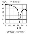
図9のグラフは、縦軸が、変形例2の幅1mmの銅の配線のアンテナでの、共振周波数fの37MHzにおける電力伝送効率Peをあらわす。横軸は(h/D)をあらわす。図9では、電力伝送効率Peは(h/D)が大きくなるとともに低下する。その理由は、(h/D)が大きくなると結合係数kが小さくなり、式24と式25であらわされる誘導抵抗r1とr2が小さくなり、式29の電力伝送効率Peが小さくなるからである。図9では、アンテナ間隔hをコイル径Dと同じ距離の50mm離した場合(h/D=1の場合)でも、電力伝送効率が約75%あり、十分効率良く電力を伝送できた。このように、家屋内の電源回路3から50mm程度の厚さの壁を隔ててコイル径Dが50mmの送信アンテナ1と受信アンテナ2を非接触で対向させて、家屋の壁に配線のための孔をあけずに、家屋外の照明装置や表示装置などの負荷回路4に約75%の効率で屋外に電力を供給する装置が製造できる。   In the graph of FIG. 9, the vertical axis represents the power transmission efficiency Pe at a resonance frequency f of 37 MHz in the antenna of copper wiring having a width of 1 mm according to the second modification. The horizontal axis represents (h / D). In FIG. 9, the power transmission efficiency Pe decreases as (h / D) increases. The reason is that as (h / D) increases, the coupling coefficient k decreases, the induction resistances r1 and r2 expressed by Expression 24 and Expression 25 decrease, and the power transmission efficiency Pe of Expression 29 decreases. In FIG. 9, even when the antenna interval h is 50 mm apart from the coil diameter D (when h / D = 1), the power transmission efficiency is about 75%, and the power can be transmitted sufficiently efficiently. In this way, the transmitting antenna 1 and the receiving antenna 2 having a coil diameter D of 50 mm are opposed to each other in a non-contact manner with a wall having a thickness of about 50 mm from the power supply circuit 3 in the house, so that the wiring is placed on the wall of the house. A device that supplies power to the load circuit 4 such as a lighting device or a display device outside the house at an efficiency of about 75% without making a hole can be manufactured.

なお、アンテナの配線のコイル(螺旋)の巻き数を増して実効的インダクタンスLを大きくすることにより、アンテナの配線の導通抵抗に比して誘導抵抗rを大きくできるので、電力伝送効率Peの式29に従って、電力伝送効率Peを大きくできる効果がある。一方、アンテナの両端を大きな容量C1とC2のコンデンサ(キャパシタンス素子)で接続すると、共振角周波数ωが小さくなり、それにより誘導抵抗rが小さくなるので、式29に従って電力伝送効率Peが小さくなる。   Note that by increasing the number of turns of the coil (spiral) of the antenna wiring and increasing the effective inductance L, the induction resistance r can be increased as compared to the conduction resistance of the antenna wiring. 29 is effective in increasing the power transmission efficiency Pe. On the other hand, when both ends of the antenna are connected by capacitors (capacitance elements) having large capacitances C1 and C2, the resonance angular frequency ω is decreased, and thereby the induction resistance r is decreased. Therefore, the power transmission efficiency Pe is decreased according to Equation 29.

(変形例3)
変形例3は、家屋の壁を隔てて電力を伝送する誘導電力伝送回路において、電力を伝送する交流の角周波数ωを低下させた誘導電力伝送回路を構成する。変形例2の送信アンテナ1と受信アンテナ2に、変形例2の4倍の400pFの端部間容量C1とC2を設置した場合をシミュレーションし、共振周波数fが変形例2の半分の約20MHzに低下させることができた。図10に、縦軸に誘導抵抗rを無次元量のr/(2πfL)であらわし、横軸にアンテナ間隔hを無次元量の(h/D)であらわすグラフを示す。図10で、黒丸印はシミュレーション結果の誘導抵抗r=r1=r2を示し、実線は近似式36の結果を示す。図10でも、シミュレーション結果は近似式36に良く一致した。
(Modification 3)
Modification 3 configures an inductive power transmission circuit in which an AC angular frequency ω for transmitting power is reduced in an inductive power transmission circuit that transmits power across a wall of a house. The case where 400 pF end-to-end capacitances C1 and C2 that are four times that of the second modification are installed in the transmission antenna 1 and the reception antenna 2 of the second modification is simulated, and the resonance frequency f is about 20 MHz, which is half that of the second modification. It was possible to reduce. FIG. 10 is a graph in which the vertical axis represents the inductive resistance r as a dimensionless amount r / (2πfL), and the horizontal axis represents the antenna interval h as a dimensionless amount (h / D). In FIG. 10, black circles indicate the inductive resistance r = r1 = r2 of the simulation result, and the solid line indicates the result of the approximate expression 36. Also in FIG. 10, the simulation result agreed well with the approximate expression 36.

(変形例4)
変形例4は、家屋の壁等の絶縁体を隔てて電力を伝送する誘導電力伝送回路において、図7の送信アンテナ1に平行に対向する受信アンテナ2をアンテナ面(XY面)内で縦横にずれ距離dずらして用いる誘導電力伝送回路を構成する。この誘導電力伝送回路において、送信アンテナ1と受信アンテナ2の端部間容量C1とC2を100pFに固定し、アンテナ間隔hを2mmに固定した場合について、種々のずれ距離dの場合についてシミュレーションして回路の整合条件を求めた。その結果を以下で説明する。この場合のアンテナ回路の共振周波数fは、変形例2と同じ37.4MHzのfoに固定した。図11に、この共振周波数f=37.4MHzにおけるシミュレーション結果を黒丸印であらわし、縦軸に誘導抵抗rを無次元量のr/(2πfL)であらわし、横軸にコイルのずれ距離dを無次元量(d/D)であらわすグラフを示す。コイルの位置を水平方向にずらすと、アンテナに現われるインピーダンスrが低下した。この原因は、コイルの位置をずらすと、コイル同士の電磁誘導の結合係数kが小さくなる為であると考える。
(Modification 4)
Modification 4 is an inductive power transmission circuit that transmits power across an insulator such as a wall of a house. A receiving antenna 2 that faces the transmitting antenna 1 in FIG. 7 parallel to the transmitting antenna 1 is vertically and horizontally within the antenna plane (XY plane). An inductive power transmission circuit used by shifting the shift distance d is configured. In this inductive power transmission circuit, simulation is performed for various displacement distances d when the end-to-end capacitances C1 and C2 of the transmitting antenna 1 and the receiving antenna 2 are fixed to 100 pF and the antenna interval h is fixed to 2 mm. The matching condition of the circuit was obtained. The results will be described below. In this case, the resonance frequency f of the antenna circuit was fixed to fo of 37.4 MHz as in the second modification. In FIG. 11, the simulation results at this resonance frequency f = 37.4 MHz are represented by black circles, the vertical axis represents the inductive resistance r by a dimensionless amount r / (2πfL), and the horizontal axis represents the coil displacement distance d. The graph represented by a dimensional quantity (d / D) is shown. When the position of the coil was shifted in the horizontal direction, the impedance r appearing on the antenna was lowered. This is considered to be because the coupling coefficient k of electromagnetic induction between the coils decreases when the position of the coils is shifted.

図12に、電源回路3から負荷回路4までの電力伝送効率(縦軸)を、横軸をコイルのずれ距離dを無次元量(d/D)であらわすグラフを示す。図12から、(d/D)が0.4以下、すなわち、コイルのずれ距離dが20mm以下ならば90%以上の電力伝送効率があり、十分効率良く電力を伝送できる。コイルのずれ距離dが(d/D)=0.66になる位置では電力伝送効率が略0になる。この位置では、一方のアンテナのコイルが発生する磁界が他方のアンテナのコイルで囲まれる面積を横切る磁界の方向がアンテナのコイル内の場所により逆になるため、磁界の総和が0になり、誘導電圧及び結合係数kが0になる為と考える。図12のように、(d/D)が0.4を超えると電力伝送効率が回復して来る。   FIG. 12 is a graph showing the power transmission efficiency (vertical axis) from the power supply circuit 3 to the load circuit 4, and the horizontal axis representing the coil shift distance d as a dimensionless amount (d / D). From FIG. 12, if (d / D) is 0.4 or less, that is, if the coil shift distance d is 20 mm or less, there is a power transmission efficiency of 90% or more, and power can be transmitted sufficiently efficiently. At a position where the coil shift distance d is (d / D) = 0.66, the power transmission efficiency is substantially zero. At this position, the direction of the magnetic field generated by the coil of one antenna across the area surrounded by the coil of the other antenna is reversed depending on the location in the coil of the antenna. This is because the voltage and the coupling coefficient k become zero. As shown in FIG. 12, when (d / D) exceeds 0.4, the power transmission efficiency is restored.

この送信アンテナ1と受信アンテナ2のコイルの軸を横方向にのみ、アンテナのコイル径D=50mmの2倍の距離の100mmずらすと、誘導抵抗rが0.23Ωになり、アンテナ系のコイルの結合係数kと等しいr/(2πfL)が0.005になり、電力伝送効率Peが20%の効率で電力を伝送できる。このように、アンテナのコイルの軸をずらす距離をアンテナのコイル径Dの2倍以下にすることで、アンテナの結合係数kが0.005以上になるので、電力伝送効率Peの飽和する周波数fの帯域幅は共振周波数foの0.5%程度あるので、0.5%程度の特性のバラツキのある部品を使っても、送信アンテナ1と受信アンテナ2の共振周波数のバラツキを許容範囲内に留めることができる。そのため、直径Dのコイルの送信アンテナ1と受信アンテナ2の間隔dを、コイルの直径Dの2倍以下にすることで実用的な誘導電力伝送回路を構成できる。 If the axes of the coils of the transmitting antenna 1 and the receiving antenna 2 are shifted 100 mm, which is twice the distance of the antenna coil diameter D = 50 mm, only in the lateral direction, the induction resistance r becomes 0.23Ω, and the coil of the antenna system R / (2πfL) equal to the coupling coefficient k is 0.005, and power can be transmitted with an efficiency of 20% as the power transmission efficiency Pe. Since the antenna coupling coefficient k becomes 0.005 or more by making the distance for shifting the axis of the antenna coil less than twice the antenna coil diameter D in this way, the frequency f at which the power transmission efficiency Pe is saturated. Is about 0.5% of the resonance frequency fo, so that even if a component having a characteristic variation of about 0.5% is used, the variation in the resonance frequency of the transmission antenna 1 and the reception antenna 2 is within an allowable range. Can be fastened. Therefore, a practical inductive power transmission circuit can be configured by setting the distance d between the transmitting antenna 1 and the receiving antenna 2 of the coil having a diameter D to be not more than twice the diameter D of the coil.

なお、送信アンテナ1と受信アンテナ2の結合係数kは0.004以上に限定されず、結合係数kがそれより小さい場合も、送信アンテナ1側で送信アンテナ1の共振周波数fを受信アンテナ2の共振周波数に同調させる回路を加えることで、効率良く電力を伝送する誘導電力伝送回路を構成できる。   Note that the coupling coefficient k between the transmission antenna 1 and the reception antenna 2 is not limited to 0.004 or more. Even when the coupling coefficient k is smaller than that, the resonance frequency f of the transmission antenna 1 is set to the value of the reception antenna 2 on the transmission antenna 1 side. By adding a circuit that is tuned to the resonance frequency, an inductive power transmission circuit that efficiently transmits power can be configured.

<第2の実施形態>
第2の実施形態は、生体外の送信アンテナ1から皮膚を隔てて生体内の受信アンテナ2まで電力を伝送する誘導電力伝送回路において、送信アンテナ1と受信アンテナ2の位置が安定せず電磁誘導の結合係数kが変動する場合に適応して安定して電力を供給する誘導電力伝送回路を構成する。この誘導電力伝送回路のアンテナは、図7の送信アンテナ1と受信アンテナ2を用いるが、それらは本発明の原理の第2の共鳴の場合で動作させる。
<Second Embodiment>
In the inductive power transmission circuit that transmits power from the transmitting antenna 1 outside the living body to the receiving antenna 2 inside the living body through the skin, the positions of the transmitting antenna 1 and the receiving antenna 2 are not stable and electromagnetic induction is performed. An inductive power transmission circuit that supplies power stably and adapts to the case where the coupling coefficient k varies is constructed. As the antenna of this induction power transmission circuit, the transmission antenna 1 and the reception antenna 2 of FIG. 7 are used, which are operated in the case of the second resonance of the principle of the present invention.

図13(a)に、図7の送信アンテナ1と受信アンテナ2の間隔h=10mm(h/D=0.2)の場合について、電源回路3と負荷回路4のインピーダンスZを変えた場合の電力伝送効率(%)をあらわす。ただし、図13(a)で、インピーダンスZをあらわす横軸は、無次元量のZ/(2πfL)であらわす。図13(a)において、実線は、電源回路3から送信アンテナ1に供給する電流I1の周波数fを37.4MHzに固定した場合の電力の伝送効率を示し、破線は、第2の実施形態の場合であり、アンテナ電流の周波数fを、最大の電力を伝送する周波数fに適合させて変えた場合の電力の伝送効率を示す。   FIG. 13A shows a case where the impedance Z between the power supply circuit 3 and the load circuit 4 is changed in the case where the distance h = 10 mm (h / D = 0.2) between the transmission antenna 1 and the reception antenna 2 in FIG. Represents the power transmission efficiency (%). However, in FIG. 13A, the horizontal axis representing the impedance Z is a dimensionless amount of Z / (2πfL). In FIG. 13A, the solid line indicates the power transmission efficiency when the frequency f of the current I1 supplied from the power supply circuit 3 to the transmitting antenna 1 is fixed at 37.4 MHz, and the broken line indicates the second embodiment. This shows the power transmission efficiency when the frequency f of the antenna current is changed to match the frequency f at which the maximum power is transmitted.

図13(b)には、特定の値のインピーダンスZにおける、誘導電力伝送回路の電力伝送効率PeをあらわすSパラメータ(S21)をdB表示であらわす。図13(b)の横軸は、アンテナ電流の周波数fをあらわす。図13(a)で、Z/(2πfL)が0.22、(このときZが9Ω)より大きい場合は、電力の伝送効率は低下する。この値0.22は電磁誘導の結合係数kに等しい。一方、Z/(2πfL)が結合係数kの0.22(このときZが9Ω)より小さい場合は、以下の2つの場合に分かれる。(1)伝送する電力の周波数fを37.4MHzに固定する場合は、電力の伝送効率は、電源回路3および負荷回路4のインピーダンスZが誘導抵抗rより低下するにつれて低下する。(2)一方、図13(b)のS21が二山になるグラフのピークを与える周波数にアンテナ電流の周波数fを調整することで、最大のS21の値(電力伝送効率Pe)で伝送するように、周波数fを適合させて変える場合は、図13(a)の破線で示すように、電力の伝送効率はほとんど低下しない。第2の実施形態では、そのように、共振の周波数fを、最大の電力伝送効率Peで伝送する周波数fに適合させて変える。   In FIG. 13B, the S parameter (S21) representing the power transmission efficiency Pe of the inductive power transmission circuit at a specific value of impedance Z is represented in dB. The horizontal axis in FIG. 13B represents the frequency f of the antenna current. In FIG. 13A, when Z / (2πfL) is larger than 0.22 (Z is 9Ω at this time), the power transmission efficiency decreases. This value 0.22 is equal to the electromagnetic induction coupling coefficient k. On the other hand, when Z / (2πfL) is smaller than the coupling coefficient k of 0.22 (in this case, Z is 9Ω), it is divided into the following two cases. (1) When the frequency f of the power to be transmitted is fixed at 37.4 MHz, the power transmission efficiency decreases as the impedance Z of the power supply circuit 3 and the load circuit 4 decreases below the induction resistance r. (2) On the other hand, by adjusting the frequency f of the antenna current to the frequency that gives the peak of the graph in which S21 in FIG. 13B becomes two peaks, the transmission is performed with the maximum value of S21 (power transmission efficiency Pe). In addition, when the frequency f is adapted and changed, the power transmission efficiency hardly decreases as shown by the broken line in FIG. In the second embodiment, the resonance frequency f is changed in accordance with the frequency f transmitted at the maximum power transmission efficiency Pe.

第2の実施形態の誘導電力伝送回路は、本発明の原理における第2の共鳴の場合の、ωがωo以外の場合に共鳴をおこす現象を利用し、送信アンテナ1と受信アンテナ2の位置が安定せず電磁誘導の結合係数kが変動する場合に適応する誘導電力伝送回路を構成する。第2の実施形態では、出力インピーダンスZ1を誘導抵抗r1の上限の値より小さな値に固定した電源回路3と、入力インピーダンスZ2をZ1×(L2/L1)の値に固定した負荷回路4を用いる。そして、送信アンテナ1と受信アンテナ2の位置の変化に伴う結合係数kの値の変化に応じて電源回路3の電流の共振角周波数ωを適応させて変えて両アンテナを共鳴させる。そのために、電源回路3から交流電力を送信アンテナ1に給電して、送信アンテナ1の共振電流を正帰還回路により電源回路3に正帰還させることで最も大きな電流を流す角周波数ωの電力を電源回路3から出力させることで、角周波数ωを、送信アンテナ1の電流I1を最も大きくする値に変える共鳴周波数調整回路を電源回路3に設置する。その角周波数ωの値は、L1×C1×(1+k・cos(β))の値の逆数の平方根の値になる。こうして、第2の実施形態の誘導電力伝送回路は電源回路3の供給する交流の角周波数ωを変えて、電力を最大の効率で伝送するように自動調整する。   The inductive power transmission circuit according to the second embodiment uses the phenomenon of resonance when ω is other than ωo in the case of the second resonance in the principle of the present invention, and the positions of the transmitting antenna 1 and the receiving antenna 2 are An inductive power transmission circuit adapted to a case where the coupling coefficient k of electromagnetic induction varies without being stable is configured. In the second embodiment, the power supply circuit 3 in which the output impedance Z1 is fixed to a value smaller than the upper limit value of the induction resistor r1 and the load circuit 4 in which the input impedance Z2 is fixed to a value of Z1 × (L2 / L1) are used. . Then, both the antennas are made to resonate by adapting and changing the resonance angular frequency ω of the current of the power supply circuit 3 in accordance with the change in the value of the coupling coefficient k accompanying the change in the position of the transmitting antenna 1 and the receiving antenna 2. For this purpose, AC power is supplied from the power supply circuit 3 to the transmission antenna 1 and the resonance current of the transmission antenna 1 is positively fed back to the power supply circuit 3 by the positive feedback circuit, thereby supplying the power of the angular frequency ω that causes the largest current to flow. A resonance frequency adjusting circuit that changes the angular frequency ω to a value that maximizes the current I 1 of the transmitting antenna 1 by being output from the circuit 3 is installed in the power supply circuit 3. The value of the angular frequency ω is the value of the square root of the reciprocal of the value of L1 × C1 × (1 + k · cos (β)). In this way, the inductive power transmission circuit of the second embodiment automatically adjusts so as to transmit power with maximum efficiency by changing the angular frequency ω of the alternating current supplied by the power supply circuit 3.

第2の実施形態では、式28に示すωを式19の値ωoからずらす場合に、位相角βをπ/2からずらし、cos(β)を0から±1にまで変え、式28の共鳴角周波数ωをωoから式41の値にまで変える。
(式41)ω≒ωo/√(1±k)
そして、sin(β)を1より小さくし0に近づけ、式24と式25に示す誘導抵抗r1とr2を上限値のkωL1およびkωL2より小さくする。このように、第2の実施形態は、共鳴角周波数ωをωoからずらすことで、式24と式25に示す小さな値の誘導抵抗r1とr2を、電源回路3の出力インピーダンスZ1と負荷回路4の負荷インピーダンスZ2に等しい値になるように調整して、電力を完全な効率で伝送する。この場合に、誘導抵抗r1とr2の比は実効的自己インダクタンスL1とL2の比になるので、電源回路の出力インピーダンスZ1と負荷回路の入力インピーダンスZ2の比は実効的自己インダクタンスL1とL2の比の固定値に設定する。このように、第2の実施形態の誘導電力伝送回路は、アンテナ間の距離が変化し安定しない場合でも、その変化に適応してアンテナ回路を共鳴させ、完全な効率の電力伝送を維持させることができる効果がある。
In the second embodiment, when ω shown in Expression 28 is shifted from the value ωo of Expression 19, the phase angle β is shifted from π / 2, cos (β) is changed from 0 to ± 1, and the resonance of Expression 28 is achieved. The angular frequency ω is changed from ωo to the value of Equation 41.
(Formula 41) ω≈ωo / √ (1 ± k)
Then, sin (β) is made smaller than 1 and brought close to 0, and the induction resistances r1 and r2 shown in Expression 24 and Expression 25 are made smaller than the upper limit values kωL1 and kωL2. As described above, in the second embodiment, the resonance angular frequency ω is shifted from ωo, so that the small inductive resistances r1 and r2 shown in Expression 24 and Expression 25 are reduced, and the output impedance Z1 of the power supply circuit 3 and the load circuit 4 are reduced. Is adjusted to a value equal to the load impedance Z <b> 2, and power is transmitted with complete efficiency. In this case, since the ratio of the inductive resistors r1 and r2 is the ratio of the effective self-inductances L1 and L2, the ratio of the output impedance Z1 of the power supply circuit and the input impedance Z2 of the load circuit is the ratio of the effective self-inductances L1 and L2. Set to a fixed value of. Thus, even when the distance between the antennas changes and is not stable, the inductive power transmission circuit of the second embodiment adapts to the change and resonates the antenna circuit to maintain perfect efficiency power transmission. There is an effect that can.

<第3の実施形態>
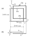
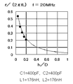
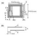
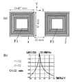
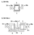
第3の実施形態は、家屋の壁を隔てて電力を伝送する誘導電力伝送回路で、アンテナの渦巻き配線の巻数を増すことでアンテナの誘導抵抗を大きくし、その誘導抵抗を電源回路3から送信アンテナ1までの電力の給電線の特性インピーダンスに近づける誘導電力伝送回路を構成する。この誘導電力伝送回路は、本発明の原理の第3の共鳴の場合の動作をさせる。図14(a)に第3の実施形態の誘導電力伝送回路の送信アンテナ1と受信アンテナ2の平面図を示し、図14(b)に側面図を示す。第1の実施形態と同様に、送信アンテナ1に電源回路3を接続し、受信アンテナ2に負荷回路4を接続する。図14では、送信アンテナ1として、厚さ50μmのポリイミドフィルム上に幅が1mmで厚さが50μmの銅の配線で形成したコイル径Dが54mmの3巻のコイルのアンテナの両端を280pFの端部間容量C1でつなぎ、アンテナの中間に電源回路3から給電する端子のポート1(P1)を設置した。受信アンテナ2は、送信アンテナ1と同じ形で同じ寸法のアンテナとし、縦横54mmの3巻のコイル状アンテナの両端を280pFの端部間容量C2でつなぎ、そのアンテナの中間に負荷回路4の端子のポート2(P2)を設置した。送信アンテナ1のコイルと受信アンテナ2のコイルは、図14(b)の側面図のように、コイル面を平行にし、コイル面(XY面)に垂直方向のアンテナ間隔hだけ離して配置し、更に、両者のコイルの軸を横(X)方向にのみ7mmのずれ距離dでずらして、縦(Y)方向にはずらさず配置した。
<Third Embodiment>
The third embodiment is an inductive power transmission circuit that transmits power across the wall of a house. The inductive resistance of the antenna is increased by increasing the number of turns of the spiral wiring of the antenna, and the inductive resistance is transmitted from the power supply circuit 3. An inductive power transmission circuit is configured to approximate the characteristic impedance of the power supply line to the antenna 1. This inductive power transmission circuit operates in the case of the third resonance according to the principle of the present invention. FIG. 14A shows a plan view of the transmitting antenna 1 and the receiving antenna 2 of the inductive power transmission circuit of the third embodiment, and FIG. 14B shows a side view. As in the first embodiment, the power supply circuit 3 is connected to the transmission antenna 1 and the load circuit 4 is connected to the reception antenna 2. In FIG. 14, as the transmitting antenna 1, both ends of the antenna of a three-coil coil having a coil diameter D of 54 mm and formed of copper wiring having a width of 1 mm and a thickness of 50 μm on a polyimide film having a thickness of 50 μm are connected to ends of 280 pF. Connected by inter-unit capacitance C1, port 1 (P1) of a terminal that feeds power from power supply circuit 3 was installed in the middle of the antenna. The receiving antenna 2 is an antenna having the same shape and the same dimensions as the transmitting antenna 1, and both ends of a coiled antenna having a length and width of 54 mm are connected by an end-to-end capacitance C2 of 280 pF, and a terminal of the load circuit 4 is interposed between the antennas. Port 2 (P2). The coil of the transmitting antenna 1 and the coil of the receiving antenna 2 are arranged so that the coil surfaces are parallel and separated from the coil surface (XY plane) by the antenna interval h in the vertical direction, as shown in the side view of FIG. Further, the axes of both coils were shifted only in the horizontal (X) direction by a shift distance d of 7 mm, and were not shifted in the vertical (Y) direction.

シミュレーションの結果、共振周波数fは9MHzになり、送信アンテナ1の実効的自己インダクタンスL1と受信アンテナ2の実効的自己インダクタンスL2は、ともに1.2μHであった。本実施形態では、送信アンテナ1と受信アンテナ2は、コイルが3巻であり、第1の実施形態のコイルの巻き数の3倍あるので、このコイルのアンテナの実効的自己インダクタンスL=L1=L2はコイルの巻き数の二乗に近い約7倍に大きくなった。そして、共振周波数f=9MHzの前後に、図3と同様な形のグラフで電力の伝送効率の周波数特性グラフを得た。この実施形態の実効的自己インダクタンスLは第1の実施形態の7倍になったので、共振の周波数fが第1の実施形態の40MHzから9MHzに下がっても、誘導抵抗rの値kωLは第1の実施形態より大きくなり、それに整合させる電源回路3及び負荷回路4のインピーダンスZを大きくできる。そして、誘導抵抗rが大きくなると、式29であらわせる電力伝送効率Peを向上させる効果がある。   As a result of the simulation, the resonance frequency f was 9 MHz, and the effective self-inductance L1 of the transmitting antenna 1 and the effective self-inductance L2 of the receiving antenna 2 were both 1.2 μH. In the present embodiment, the transmitting antenna 1 and the receiving antenna 2 have three coils, which is three times the number of turns of the coil of the first embodiment, so that the effective self-inductance L = L1 = L2 became about 7 times as large as the square of the number of turns of the coil. Then, before and after the resonance frequency f = 9 MHz, a frequency characteristic graph of power transmission efficiency was obtained with a graph having the same shape as in FIG. Since the effective self-inductance L of this embodiment is seven times that of the first embodiment, the value kωL of the inductive resistance r remains the same even when the resonance frequency f decreases from 40 MHz to 9 MHz of the first embodiment. The impedance Z of the power supply circuit 3 and the load circuit 4 matched with that of the first embodiment can be increased. When the induction resistance r increases, there is an effect of improving the power transmission efficiency Pe expressed by Equation 29.

図15(a)に、第3の実施形態の共振周波数f=9MHzにおける誘導抵抗rを無次元量のr/(2πfL)にして縦軸であらわし、横軸にアンテナ間隔hを無次元量の(h/D)であらわすグラフを示す。図15(a)で、黒丸印はシミュレーション結果を示し、実線は、近似式36の値を示す。図15(a)は、シミュレーション結果は近似式36に概ね一致した。図15(b)に、縦軸に電源回路3から負荷回路4までの電力伝送効率をあらわし、横軸にアンテナ間隔hを無次元量(h/D)であらわすグラフを示す。図15(b)から、アンテナ間隔hをコイル径Dの6割程度の約30mm離した場合(h/D=0.6の場合)でも、電力伝送効率が約90%あり十分効率良く電力を伝送できる。   In FIG. 15A, the inductive resistance r at the resonance frequency f = 9 MHz of the third embodiment is expressed as a dimensionless amount r / (2πfL), and the abscissa represents the antenna interval h as the dimensionless amount. The graph represented by (h / D) is shown. In FIG. 15A, the black circles indicate the simulation results, and the solid line indicates the value of the approximate expression 36. In FIG. 15 (a), the simulation result almost coincides with the approximate expression 36. FIG. 15B shows a graph in which the vertical axis represents the power transmission efficiency from the power supply circuit 3 to the load circuit 4, and the horizontal axis represents the antenna interval h as a dimensionless amount (h / D). From FIG. 15 (b), even when the antenna interval h is about 30 mm, which is about 60% of the coil diameter D (when h / D = 0.6), the power transmission efficiency is about 90% and the power can be sufficiently efficiently supplied. Can be transmitted.

(変形例5)
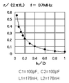
変形例5は、第3の実施形態の送信アンテナ1と受信アンテナ2それぞれの両端をつなぐ端部間容量C1とC2の容量を第3の実施形態の容量の16分の1の17pFにして共振周波数fを高くした場合を示す。変形例5の場合は共振周波数f=35MHzで共振した。図16(a)に、その場合の誘導抵抗rを無次元量のr/(2πfL)にして縦軸であらわし、横軸にアンテナ間隔hを無次元量の(h/D)であらわすグラフを示す。このように、端部間容量C1とC2の容量を約16分の1に小さくすると、共振周波数fは約4倍の35MHzに大きくなった。図16(a)は、黒丸印で示すシミュレーション結果は実線で示す近似式36に概ね一致した。図16(b)に、縦軸に電源回路3から負荷回路4までの電力伝送効率をあらわし、横軸にアンテナ間隔hを無次元量(h/D)であらわすグラフを示す。図16(b)から、アンテナ間隔hをコイル径Dの8割程度の約40mm離した場合(h/D=0.8の場合)でも、電力伝送効率が約90%あり十分効率良く電力を伝送できる。図16(a)から、アンテナ間隔hを1mm離して(h/D)を約0.6にする場合に、r/(2πfL)=結合係数kが0.6になり誘導抵抗rが158Ωに高くなる。この実施形態の実効的インダクタンスLは第1の実施形態の7倍になったので、第1の実施形態の40MHzとほぼ同じ周波数fの35MHzの場合では、誘導抵抗rの値kωLは第1の実施形態の7倍に大きくなり、それに整合させる電源回路3及び負荷回路4のインピーダンスZが7倍に大きくなる。そして、誘導抵抗rが大きくなるので式29であらわせる電力伝送効率Peを向上させる効果がある。
(Modification 5)
In the fifth modification, the capacitance of the end-to-end capacitances C1 and C2 connecting both ends of the transmission antenna 1 and the reception antenna 2 of the third embodiment is set to 17 pF, which is 1/16 of the capacitance of the third embodiment. A case where the frequency f is increased is shown. In the case of the modified example 5, resonance occurred at a resonance frequency f = 35 MHz. FIG. 16A is a graph in which the induction resistance r in that case is represented as a dimensionless amount r / (2πfL), and the abscissa represents the antenna interval h as a dimensionless amount (h / D). Show. As described above, when the end-to-end capacities C1 and C2 were reduced to about 1/16, the resonance frequency f was increased to about 4 times 35 MHz. In FIG. 16 (a), the simulation result indicated by the black circle generally matches the approximate expression 36 indicated by the solid line. FIG. 16B shows a graph in which the vertical axis represents the power transmission efficiency from the power supply circuit 3 to the load circuit 4 and the horizontal axis represents the antenna interval h as a dimensionless amount (h / D). From FIG. 16 (b), even when the antenna interval h is about 40 mm, which is about 80% of the coil diameter D (when h / D = 0.8), the power transmission efficiency is about 90%, and the power can be sufficiently efficiently supplied. Can be transmitted. From FIG. 16A, when the antenna interval h is 1 mm apart and (h / D) is set to about 0.6, r / (2πfL) = coupling coefficient k becomes 0.6 and the induction resistance r becomes 158Ω. Get higher. Since the effective inductance L of this embodiment is seven times that of the first embodiment, the value kωL of the inductive resistance r is the first value in the case of 35 MHz, which is substantially the same frequency f as 40 MHz of the first embodiment. The impedance Z of the power supply circuit 3 and the load circuit 4 to be matched is increased seven times as much as that in the embodiment. And since the induction resistance r becomes large, there is an effect of improving the power transmission efficiency Pe expressed by the equation 29.

<第4の実施形態>
第4の実施形態は、第3の実施形態のアンテナの両端に外部コンデンサを加えずに共振周波数fを高くすることでアンテナの誘導抵抗を高くし、電源回路3から送信アンテナ1までの電力の給電線に特性インピーダンスの高い給電線を用いる誘導電力伝送回路を構成する。すなわち、第4の実施形態では、図14の送信アンテナ1と受信アンテナ2の両端を開放し、アンテナの端部間に外部コンデンサは加えない。しかし、アンテナ端部間には、寄生容量値minの容量C1とC2がある。この誘導電力伝送回路も本発明の原理の第3の共鳴の場合の動作をさせる。第4の実施形態の誘導電力伝送回路のアンテナ系は、周波数f=154MHzで共振する。共振周波数f=154MHzと、外部コンデンサを加えた場合に得たアンテナのコイルの実効的自己インダクタンスL=1.2μHとから計算すると、このアンテナのコイルの両端は実効的に約1pFの寄生容量値minでつながれていることがわかる。このため、アンテナのコイル端を開放した状態でも、図2(a)の回路であって、送信アンテナ1と受信アンテナ2それぞれのアンテナの両端に約1pFの容量C1とC2をつないだ回路である。
<Fourth Embodiment>
The fourth embodiment increases the induction resistance of the antenna by increasing the resonance frequency f without adding an external capacitor to both ends of the antenna of the third embodiment, and the power from the power supply circuit 3 to the transmission antenna 1 is increased. An inductive power transmission circuit that uses a power supply line with high characteristic impedance as the power supply line is configured. That is, in the fourth embodiment, both ends of the transmission antenna 1 and the reception antenna 2 in FIG. 14 are opened, and no external capacitor is added between the ends of the antenna. However, between the antenna ends, there are capacitors C1 and C2 having a parasitic capacitance value min. This inductive power transmission circuit also operates in the case of the third resonance according to the principle of the present invention. The antenna system of the inductive power transmission circuit according to the fourth embodiment resonates at a frequency f = 154 MHz. When calculating from the resonance frequency f = 154 MHz and the effective self-inductance L = 1.2 μH of the antenna coil obtained when an external capacitor is added, both ends of the antenna coil are effectively parasitic capacitance values of about 1 pF. It turns out that it is connected by min. Therefore, even when the coil end of the antenna is opened, the circuit shown in FIG. 2A is a circuit in which capacitances C1 and C2 of about 1 pF are connected to both ends of the antennas of the transmitting antenna 1 and the receiving antenna 2, respectively. .

図17(a)に、第4の実施形態の共振周波数f=154MHzにおける誘導抵抗rを無次元量のr/(2πfL)にして縦軸であらわし、横軸にアンテナ間隔hを無次元量の(h/D)であらわすグラフを示す。ここでr/(2πfL)を計算する基礎にするLの値としては、外部コンデンサを加えた場合に得たアンテナのコイルの実効的自己インダクタンスL=1.2μHを用いた。黒丸印はシミュレーション結果を示し、点線は近似式36の値×(2/π)を示す。アンテナ端部間に寄生容量以外には外部コンデンサを加えずアンテナ端を開放した場合は、アンテナ電流分布がアンテナの端部間を個別のコンデンサで接続した場合と異なり、アンテナの端部に近づくにつれアンテナ電流が小さくなる。そして、アンテナ電流の平均値がアンテナの中間のポートでの電流値の(2/π)倍になる。そのため、点線のグラフは、アンテナ電流の平均値のポート電流に対する減少分を補正するために近似式36の右辺の式に(2/π)を掛け算した値を示す。その補正結果の値がシミュレーション結果に一致した。この補正が必要になった理由は、アンテナ端を開放した場合のアンテナのコイルの実効的自己インダクタンスLは、外部コンデンサを加えた場合に得たアンテナのコイルの実効的自己インダクタンスLとは変わってしまうことに依ると考える。近似式36に用いるLは、アンテナ電流の分布に応じて変化する実行的自己インダクタンスLを用いるべきである。このアンテナでアンテナ端を開放した場合の実効的インダクタンスLの値は、アンテナ端に大きな容量を接続した場合の実効的インダクタンスの値の概ね(2/π)倍になるので、近似式36を用いる場合にLの値として、外部コンデンサを加えた場合に得た実効的自己インダクタンスLを用いる場合は、計算結果を補正する必要がある考える。   In FIG. 17A, the inductive resistance r at the resonance frequency f = 154 MHz of the fourth embodiment is expressed as a dimensionless amount r / (2πfL), and the abscissa represents the antenna interval h as the dimensionless amount. The graph represented by (h / D) is shown. Here, as the value of L used as a basis for calculating r / (2πfL), the effective self-inductance L = 1.2 μH of the coil of the antenna obtained when an external capacitor is added was used. Black circles indicate simulation results, and dotted lines indicate the value of the approximate expression 36 × (2 / π). When the antenna end is opened without adding an external capacitor other than the parasitic capacitance between the antenna ends, the antenna current distribution differs from the case where the antenna ends are connected by individual capacitors, as the antenna ends are approached. The antenna current is reduced. The average value of the antenna current is (2 / π) times the current value at the intermediate port of the antenna. Therefore, the dotted line graph represents a value obtained by multiplying the expression on the right side of the approximate expression 36 by (2 / π) in order to correct the decrease of the average value of the antenna current with respect to the port current. The value of the correction result coincided with the simulation result. The reason why this correction is necessary is that the effective self-inductance L of the antenna coil when the antenna end is opened is different from the effective self-inductance L of the antenna coil obtained when an external capacitor is added. I think that it depends on. The effective self-inductance L that changes according to the distribution of the antenna current should be used as L used in the approximate expression 36. Since the effective inductance L when the antenna end is opened with this antenna is approximately (2 / π) times the effective inductance when a large capacitance is connected to the antenna end, the approximate expression 36 is used. In this case, when the effective self-inductance L obtained when an external capacitor is added is used as the value of L, the calculation result needs to be corrected.

図17(a)から、アンテナ間隔hを4mm離して(h/D)を0.074にする場合に、r/(2πfL)が0.22になり誘導抵抗rが260Ωになる。第4の実施形態では、アンテナ間隔hを約4mm離すことで、誘導抵抗rを約260Ωにする。この誘導抵抗rには、平行2線の給電線の特性インピーダンスが良く整合する。平行2線の給電線の特性インピーダンスは、給電線の2線間の距離が給電線の半径の10倍の場合は給電線の特性インピーダンスが277Ωになり260Ωの誘導抵抗rに近いからである。第4の実施形態では、誘導抵抗rを高くしそれに整合する電源回路3と給電線の特性インピーダンスを高くしたので、電力を伝送するための電流が少なくなり給電線の導体抵抗に電流が流れることによる損失を少なくできる効果がある。   From FIG. 17A, when the antenna interval h is 4 mm apart and (h / D) is 0.074, r / (2πfL) is 0.22, and the induction resistance r is 260Ω. In the fourth embodiment, the induction resistance r is set to about 260Ω by separating the antenna interval h by about 4 mm. The characteristic impedance of the parallel two-wire feed line is well matched with the induction resistance r. This is because the characteristic impedance of the two parallel feed lines is close to the induction resistance r of 260Ω when the distance between the two feed lines is 10 times the radius of the feed line and the characteristic impedance of the feed line is 277Ω. In the fourth embodiment, the inductive resistance r is increased and the characteristic impedance of the power supply circuit 3 and the feeder line matched therewith is increased, so that the current for transmitting power is reduced and the current flows through the conductor resistance of the feeder line. There is an effect that the loss due to can be reduced.

図17(b)に、縦軸に電源回路3から負荷回路4までの電力伝送効率をあらわし、横軸にアンテナ間隔hを無次元量(h/D)であらわすグラフを示す。図17(b)から、アンテナ間隔hをコイル径Dの8割(h/D=0.8)の43mm程度離した場合でも、電力伝送効率が約90%あり十分効率良く電力を伝送できる。   FIG. 17B is a graph in which the vertical axis represents the power transmission efficiency from the power supply circuit 3 to the load circuit 4 and the horizontal axis represents the antenna interval h as a dimensionless amount (h / D). From FIG. 17B, even when the antenna interval h is about 43 mm, which is 80% of the coil diameter D (h / D = 0.8), the power transmission efficiency is about 90% and power can be transmitted sufficiently efficiently.

<第5の実施形態>
第5の実施形態は、本発明の原理の第2の共鳴の場合を利用して、変成器を成す誘導電力伝送回路を構成する。すなわち、図2(a)の回路であって、空芯コイルの送信アンテナ1と受信アンテナ2を共鳴電磁界の波長の2π分の1より近い距離に設置し、コイルの巻き数を変えて実効的自己インダクタンスL1とL2を変えることで、電源回路3の出力インピーダンスZ1を、(L2/L1)倍の、負荷回路4の負荷インピーダンスZ2に変換する変成器を成す誘導電力伝送回路を構成する。第5の実施形態は、共振角周波数ωがωoと異なる場合の本発明の原理の第2の共鳴の場合には、アンテナのコイルの誘導抵抗rが、式24と式25に従って、アンテナの配線のコイル(巻線)の実効的自己インダクタンスLに比例して変わり、その比例係数は結合係数kと2πfとsin(β)の積であることを利用した。この変成器は、送信アンテナ1側に接続した電源回路3のkωL1以下のインピーダンスを、受信アンテナ側で見るとkωL2以下の出力インピーダンスに変換できる効果がある。本実施形態で、ポリイミドフィルム上に銅の配線をエッチングして螺旋状のパターン形成した空芯コイルの送信アンテナ1と受信アンテナ2の間隔に磁性体を設けず、アンテナ同士を空気中(あるいは絶縁体中)で対向させ近づけると、結合係数kが大きくなり、インピーダンス変換できるインピーダンスの値の上限が大きくなるので、両アンテナを空気中(あるいは絶縁樹脂などの絶縁体中)で近づけることが望ましい。この変成器では、送信アンテナ1の実効的自己インダクタンスL1と受信アンテナ2の実効的自己インダクタンスL2を、アンテナのコイルの巻数を変えて調整することでインピーダンスの変換率(L2/L1)を調整する。アンテナの配線のコイルの実効的自己インダクタンスLは、概ね巻数の二乗に比例して変わる。このように、第5の実施形態の変成器は、異なるインピーダンスZ1を持つ電源回路3と負荷回路4のインピーダンスZ2を変換して、電源回路3から負荷回路4へ略100%の電力を伝送する誘導電力伝送回路である。
<Fifth Embodiment>
The fifth embodiment uses the second resonance case of the principle of the present invention to configure an inductive power transmission circuit constituting a transformer. That is, in the circuit of FIG. 2 (a), the transmitting antenna 1 and the receiving antenna 2 of the air-core coil are installed at a distance closer than 1 / 2π of the wavelength of the resonance electromagnetic field, and the number of turns of the coil is changed. By changing the static self-inductances L1 and L2, an inductive power transmission circuit constituting a transformer for converting the output impedance Z1 of the power supply circuit 3 into the load impedance Z2 of the load circuit 4 that is (L2 / L1) times is configured. In the fifth embodiment, in the case of the second resonance according to the principle of the present invention when the resonance angular frequency ω is different from ωo, the induction resistance r of the coil of the antenna is determined according to Equation 24 and Equation 25. It is utilized in proportion to the effective self-inductance L of the coil (winding), and the proportionality coefficient is the product of the coupling coefficient k, 2πf and sin (β). This transformer has an effect that the impedance of kωL1 or less of the power supply circuit 3 connected to the transmitting antenna 1 side can be converted to an output impedance of kωL2 or less when viewed on the receiving antenna side. In this embodiment, a magnetic material is not provided in the space between the transmitting antenna 1 and the receiving antenna 2 of the air-core coil formed by etching a copper wiring on the polyimide film to form a spiral pattern. Since the coupling coefficient k increases and the upper limit of the impedance value that can be converted into impedance increases, it is desirable to bring both antennas close to each other in the air (or in an insulator such as an insulating resin). In this transformer, the impedance conversion rate (L2 / L1) is adjusted by adjusting the effective self-inductance L1 of the transmitting antenna 1 and the effective self-inductance L2 of the receiving antenna 2 by changing the number of turns of the coil of the antenna. . The effective self-inductance L of the antenna wiring coil changes approximately in proportion to the square of the number of turns. As described above, the transformer according to the fifth embodiment converts the impedance Z2 of the power circuit 3 and the load circuit 4 having different impedances Z1, and transmits approximately 100% of the power from the power circuit 3 to the load circuit 4. Inductive power transmission circuit.

第5の実施形態の変成器は電源回路3の出力インピーダンスZ1を送信アンテナ1の誘導抵抗r1に一致させ、負荷回路4の入力インピーダンスZ2を受信アンテナ2の誘導抵抗r2に一致させる。誘導抵抗r1とr2は式24と式25のsin(β)を小さくすることで小さくしてインピーダンスZ1とZ2に整合させる。その整合条件を満たす共鳴の角周波数ωはそのβの値に従って、式28であらわされるように、ωoから式41の値(ωo/√(1±k))にまで変わる。式28の共振角周波数ωは、cos(β)が負の共鳴条件の場合は、ωoより高い角周波数にシフトし、図13(b)の二山のグラフの右の山のピークを与える角周波数になる。受信アンテナ2の電流I2は送信アンテナ1の電流I1を打ち消すように逆向きに流れ、送信アンテナ1と受信アンテナ2の総体のアンテナ系が外部に発生する電磁界が小さくなり、この変成器の発生する不要電磁波ノイズ(EMI)が小さくなる効果がある。   The transformer according to the fifth embodiment makes the output impedance Z1 of the power supply circuit 3 coincide with the induction resistance r1 of the transmission antenna 1, and makes the input impedance Z2 of the load circuit 4 coincide with the induction resistance r2 of the reception antenna 2. The inductive resistances r1 and r2 are made smaller by reducing sin (β) in the expressions 24 and 25 to match the impedances Z1 and Z2. The resonance angular frequency ω that satisfies the matching condition changes from ωo to the value of Equation 41 (ωo / √ (1 ± k)) as represented by Equation 28 according to the value of β. The resonance angular frequency ω of Expression 28 is shifted to an angular frequency higher than ωo when cos (β) is a negative resonance condition, and the angle that gives the peak of the right peak in the two-peak graph of FIG. Become a frequency. The current I2 of the receiving antenna 2 flows in the opposite direction so as to cancel the current I1 of the transmitting antenna 1, and the electromagnetic field generated by the overall antenna system of the transmitting antenna 1 and the receiving antenna 2 is reduced, and this transformer is generated. This is effective in reducing unnecessary electromagnetic noise (EMI).

また、cos(β)が正の共鳴条件の場合は、共振角周波数ωはωoより低い角周波数にシフトし、図13(b)の二山のグラフの左の山のピークを与える角周波数になる。受信アンテナ2の電流I2は送信アンテナ1の電流I1と同じ方向に流れ、送信アンテナ1と受信アンテナ2の総体のアンテナ系が外部に発生する電磁界が大きくなる問題があるが、その一方、1つの送信アンテナ1のアンテナ配線のコイルの軸に、アンテナ配線のコイルの軸を共有する複数の受信アンテナ2を平行に設置して、同時に複数の受信アンテナ2の回路に無線電力を給電できる効果がある。   When cos (β) is a positive resonance condition, the resonance angular frequency ω is shifted to an angular frequency lower than ωo, and the angular frequency giving the peak of the left mountain in the two-crest graph of FIG. Become. The current I2 of the receiving antenna 2 flows in the same direction as the current I1 of the transmitting antenna 1, and there is a problem that the electromagnetic field generated by the overall antenna system of the transmitting antenna 1 and the receiving antenna 2 becomes large. There is an effect that a plurality of receiving antennas 2 sharing the axis of the coil of the antenna wiring can be installed in parallel to the axis of the coil of the antenna wiring of the two transmitting antennas 1 and wireless power can be supplied to the circuits of the plurality of receiving antennas 2 at the same time. is there.

なお、空芯コイルの送信アンテナ1と受信アンテナ2を(共鳴電磁界の波長)/(2π)よりも近い距離に設置して構成する第5の実施形態の変成器は、空芯コイルを空気中あるいは絶縁樹脂中で対向させて用いると、従来の変成器に比べ、重量と寸法を軽減できる効果がある。また、第5の実施形態の変成器は、コアに強磁性体の材料を用いる従来の変成器がその強磁性体の周波数特性により制約されて使えなかった高周波においても、制約無く変成器を構成できる効果がある。   Note that the transformer of the fifth embodiment in which the transmitting antenna 1 and the receiving antenna 2 of the air-core coil are installed at a distance closer than (wavelength of the resonance electromagnetic field) / (2π) is the air transformer in which the air-core coil is the air. When used in the middle or in an insulating resin, the weight and dimensions can be reduced as compared with a conventional transformer. Further, the transformer according to the fifth embodiment is configured without restriction even at a high frequency where a conventional transformer using a ferromagnetic material for the core is restricted due to the frequency characteristics of the ferromagnetic material. There is an effect that can be done.

<第6の実施形態>
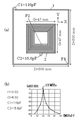
本発明の第6の実施形態は、集積回路の配線層間に電力を伝送する誘導電力伝送回路を構成する。図18(a)に、第6の実施形態の送信アンテナ1と受信アンテナ2の平面図を示し、図18(b)に側面図を示す。この誘導電力伝送回路は、本発明の原理の第3の共鳴の場合の動作をさせる。送信アンテナ1の配線の中間に電源回路3の端子のポート1(P1)を設置し、受信アンテナ2の配線の中間に負荷回路4の端子のポート2(P2)を設置する。図18では、送信アンテナ1と受信アンテナ2として、集積回路チップの配線層に形成した、厚さが1μmの銅で、第3の実施形態の1000分の1の寸法のコイルを用いた。すなわち、送信アンテナ1と受信アンテナ2は、配線幅が1μmでコイル径D及びGが54μmの3巻のコイルを用いた。このアンテナのコイルは集積回路チップ内の絶縁樹脂等の上層に形成したグローバル配線層に形成することが望ましい。また、このアンテナのコイル状の配線の両端は開放してその両端間は寄生容量値minの容量C1とC2で結合させる。集積回路チップの配線層に受信アンテナ2の配線を形成し、その集積回路を設置する基板の配線層に送信アンテナ1の銅の配線を形成し、基板側から集積回路チップに無線で電力を供給する誘導電力伝送回路が構成できる。図18(b)の側面図のように、送信アンテナ1のコイルと受信アンテナ2のコイルは、両者のコイルの軸を横(X)方向にのみ7μmのずれ距離dでずらして、縦(Y)方向にはずらさず、コイルの面に平行にアンテナ間隔hを保って配置した。
<Sixth Embodiment>
The sixth embodiment of the present invention constitutes an inductive power transmission circuit that transmits power between wiring layers of an integrated circuit. FIG. 18A shows a plan view of the transmitting antenna 1 and the receiving antenna 2 of the sixth embodiment, and FIG. 18B shows a side view. This inductive power transmission circuit operates in the case of the third resonance according to the principle of the present invention. The port 1 (P1) of the terminal of the power supply circuit 3 is installed in the middle of the wiring of the transmitting antenna 1, and the port 2 (P2) of the terminal of the load circuit 4 is installed in the middle of the wiring of the receiving antenna 2. In FIG. 18, the transmission antenna 1 and the reception antenna 2 are made of copper having a thickness of 1 μm and having a thickness of 1/1000 of that of the third embodiment, which is formed in the wiring layer of the integrated circuit chip. That is, for the transmission antenna 1 and the reception antenna 2, three winding coils having a wiring width of 1 μm and coil diameters D and G of 54 μm were used. The antenna coil is preferably formed on a global wiring layer formed on an insulating resin or the like in the integrated circuit chip. Also, both ends of the coiled wiring of the antenna are opened and the ends are coupled by capacitors C1 and C2 having a parasitic capacitance value min. The wiring of the receiving antenna 2 is formed on the wiring layer of the integrated circuit chip, the copper wiring of the transmitting antenna 1 is formed on the wiring layer of the substrate on which the integrated circuit is installed, and power is supplied to the integrated circuit chip wirelessly from the substrate side. An inductive power transmission circuit can be configured. As shown in the side view of FIG. 18B, the coil of the transmitting antenna 1 and the coil of the receiving antenna 2 are shifted vertically (Y) by shifting the axes of the coils only in the lateral (X) direction by a deviation distance d of 7 μm. The antenna spacing h is arranged in parallel to the coil surface without shifting in the direction.

図19(a)に、この場合の共振周波数f=140GHzにおける誘導抵抗rを無次元量のr/(2πfL)にして縦軸であらわし、横軸にアンテナ間隔hを無次元量の(h/D)であらわすグラフを示す。このアンテナのコイルの実効的自己インダクタンスLは1.3nHであり、このアンテナのコイルの両端は実効的に約0.001pFの寄生容量値minでつながれた。図19(a)で、黒丸印はシミュレーション結果を示し、点線は近似式13の値×(2/π)を示す。このグラフは、第4の実施形態の結果と同様に黒丸印のシミュレーション結果が点線のグラフに一致した。アンテナ間隔hをコイル径Dの2割(h/D=0.2)程度の約10μm離す場合はr/(2πfL)が0.12で誘導抵抗rが約140Ωあり、アンテナ間隔hをコイル径Dの4割(h/D=0.4)程度の約20μm離す場合はr/(2πfL)が0.08で誘導抵抗rが約90Ωある。電源回路3及び負荷回路4のインピーダンスはこれらの誘導抵抗に整合させる。図19(b)に、縦軸に電源回路3から負荷回路4までの電力伝送効率をあらわし、横軸にアンテナ間隔hを無次元量(h/D)であらわす。図19(b)から、アンテナ間隔hをコイル径Dの2割(h/D=0.2)程度の約10μm離す場合、電力伝送効率が約80%あり十分効率良く電力を伝送できる。コイル径Dの4割(h/D=0.4)程度の約20μm離す場合も電力伝送効率が約60%ある。この現象を利用して、半導体集積回路内に54μm程度の直径のコイル状の送信アンテナ1と受信アンテナ2間のアンテナ間隔hを10μmから20μm離してアンテナを対向させて非接触で効率良く電力を伝送する回路を構成できる。また、電力を伝送する信号層間の距離、すなわちアンテナ間隔hを数倍大きくする場合は、アンテナの直径Dを数倍に大きくすることで、効率良く電力を伝送する誘導電力伝送回路を構成できる。また、集積回路チップの配線層に受信アンテナ2の配線を形成し、その集積回路を設置する基板の配線層に送信アンテナ1の銅の配線を形成する場合に、図23の例のように、基板側の送信アンテナ1の寸法を集積回路チップ側の受信アンテナ2の寸法より大きく形成することもできる。。   In FIG. 19A, the inductive resistance r at the resonance frequency f = 140 GHz in this case is expressed as a dimensionless amount r / (2πfL) on the vertical axis, and the antenna interval h is plotted on the horizontal axis as a dimensionless amount (h / The graph represented by D) is shown. The effective self-inductance L of the coil of this antenna was 1.3 nH, and both ends of the coil of this antenna were effectively connected with a parasitic capacitance value min of about 0.001 pF. In FIG. 19A, the black circles indicate the simulation results, and the dotted lines indicate the value of the approximate expression 13 × (2 / π). In this graph, similar to the result of the fourth embodiment, the simulation result indicated by the black circle coincides with the dotted line graph. When the antenna interval h is about 10 μm apart, which is about 20% of the coil diameter D (h / D = 0.2), r / (2πfL) is 0.12, the induction resistance r is about 140Ω, and the antenna interval h is the coil diameter. When about 20 μm, which is about 40% of D (h / D = 0.4), r / (2πfL) is 0.08 and the induction resistance r is about 90Ω. The impedances of the power supply circuit 3 and the load circuit 4 are matched to these inductive resistors. In FIG. 19B, the vertical axis represents the power transmission efficiency from the power supply circuit 3 to the load circuit 4, and the horizontal axis represents the antenna interval h as a dimensionless amount (h / D). From FIG. 19B, when the antenna interval h is about 10 μm, which is about 20% of the coil diameter D (h / D = 0.2), the power transmission efficiency is about 80% and power can be transmitted sufficiently efficiently. The power transmission efficiency is about 60% even when the coil diameter D is about 20 μm, which is about 40% of the coil diameter D (h / D = 0.4). By utilizing this phenomenon, the antenna interval h between the coiled transmitting antenna 1 and the receiving antenna 2 having a diameter of about 54 μm is separated from 10 μm to 20 μm in the semiconductor integrated circuit, and the antennas are opposed to each other so as to efficiently supply power without contact. A circuit for transmission can be configured. Further, when the distance between signal layers for transmitting power, that is, the antenna interval h is increased several times, an induction power transmission circuit that efficiently transmits power can be configured by increasing the antenna diameter D several times. Further, when the wiring of the receiving antenna 2 is formed in the wiring layer of the integrated circuit chip and the copper wiring of the transmitting antenna 1 is formed in the wiring layer of the substrate on which the integrated circuit is installed, as in the example of FIG. The size of the transmitting antenna 1 on the substrate side can be made larger than the size of the receiving antenna 2 on the integrated circuit chip side. .

<第7の実施形態>
第7の実施形態は、電源回路3に直径が約300mmの送信アンテナ1を接続し、電子ディスプレイ装置に埋め込んだ約300mmの直径の受信アンテナ2までの空間を電力を伝送し、その受信アンテナ2に電子ディスプレイ装置の負荷回路4を接続して電子ディスプレイ装置を動作させる誘導電力伝送回路を構成する。この誘導電力伝送回路も本発明の原理の第3の共鳴の場合の動作をさせる。第7の実施形態では、第3の実施形態の図14(a)の3巻きのコイル状のアンテナの寸法を約6倍の300mmに拡大し、厚さ50μmで幅が10mmの銅の配線を3巻きした送信アンテナ1と受信アンテナ2を対向させてアンテナ間に電力を伝送する。このアンテナ配線は、ポリイミドフィルムに厚さ50μmで積層した銅箔をエッチングすることで形成することができる。この各アンテナのコイルの実効的自己インダクタンスL1とL2は4.9μHである。各アンテナコイルの配線の両端に100pFの容量C1とC2を接続する。この場合は、共振周波数fが7.3MHzになる。送信アンテナ1と受信アンテナ2のアンテナ間隔hをアンテナの寸法D程度の300mm離した場合に、両アンテナの結合係数kが約0.02になり、誘導抵抗r1とr2が約4Ωになる。この整合した回路での電力伝送効率Peは約94%になり電力が効率良く伝送できる。
<Seventh Embodiment>
In the seventh embodiment, a transmission antenna 1 having a diameter of about 300 mm is connected to a power supply circuit 3, and power is transmitted through a space up to a reception antenna 2 having a diameter of about 300 mm embedded in an electronic display device. The load circuit 4 of the electronic display device is connected to the inductive power transmission circuit for operating the electronic display device. This inductive power transmission circuit also operates in the case of the third resonance according to the principle of the present invention. In the seventh embodiment, the size of the three-turn coiled antenna of FIG. 14A of the third embodiment is increased to about 6 times by 300 mm, and copper wiring having a thickness of 50 μm and a width of 10 mm is formed. The transmitting antenna 1 and the receiving antenna 2 that are wound three times are opposed to each other, and power is transmitted between the antennas. This antenna wiring can be formed by etching a copper foil laminated on a polyimide film with a thickness of 50 μm. The effective self-inductances L1 and L2 of the coils of each antenna are 4.9 μH. Capacitors C1 and C2 of 100 pF are connected to both ends of the wiring of each antenna coil. In this case, the resonance frequency f is 7.3 MHz. When the antenna interval h between the transmitting antenna 1 and the receiving antenna 2 is about 300 mm apart from the antenna dimension D, the coupling coefficient k of both antennas is about 0.02, and the induction resistances r1 and r2 are about 4Ω. The power transmission efficiency Pe in this matched circuit is about 94%, and power can be transmitted efficiently.

この電力伝送効率Peが良い原因は、アンテナの寸法が大きくなって共振周波数fが低くなったため、アンテナ配線の表皮効果による損失が小さくなったからである。このように大きな寸法のアンテナを用いて電子ディスプレイ装置に電力を供給することで、送信アンテナ1と受信アンテナ2のアンテナ間隔hを大きく取っても電力を効率良く電子ディスプレイ装置に伝送できる効果がある。   The reason why the power transmission efficiency Pe is good is that the loss due to the skin effect of the antenna wiring is reduced because the dimensions of the antenna are increased and the resonance frequency f is decreased. By supplying power to the electronic display device using the antenna having such a large size, there is an effect that the power can be efficiently transmitted to the electronic display device even when the antenna interval h between the transmitting antenna 1 and the receiving antenna 2 is large. .

(変形例6)
変形例6は、直径が300mmの大きなアンテナを用いて、電力を動力として利用する車両などに電力を供給する誘導電力伝送回路を構成する。すなわち、変形例6では、電力供給設備の電源回路3から電力を、周波数が約7.3MHzの高周波電流にして、幅10mmの銅の配線の3巻きの矩形のコイルで直径Dが300mmの送信アンテナ1に電流を供給し、その送信アンテナ1から300mm程度の距離を隔てて対向する車両の受信アンテナ2に約94%の効率で電力を送信し、その受信アンテナ2から、その電力をその車両の充電池などの負荷回路4に伝送する誘導電力伝送回路を提案する。
(Modification 6)
In the sixth modification, an inductive power transmission circuit that supplies electric power to a vehicle or the like that uses electric power as power is configured using a large antenna having a diameter of 300 mm. That is, in the modified example 6, the power from the power supply circuit 3 of the power supply facility is changed to a high-frequency current having a frequency of about 7.3 MHz, and a three-turn rectangular coil of copper wiring having a width of 10 mm is used to transmit a diameter D of 300 mm. A current is supplied to the antenna 1, and power is transmitted to the receiving antenna 2 of the vehicle opposed to the transmitting antenna 1 at a distance of about 300 mm with an efficiency of about 94%, and the power is transmitted from the receiving antenna 2 to the vehicle. An inductive power transmission circuit for transmitting to a load circuit 4 such as a rechargeable battery is proposed.

<第8の実施形態>
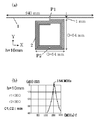
第8の実施形態は、例えば携帯電話などの電子機器に非接触で電力を伝送する回路として、図20(a)の平面図のように、送信アンテナ1と受信アンテナ2を同一平面上に並べて配置して電力を伝送する誘導電力伝送回路を構成する。すなわち、縦横47mmの矩形の送信アンテナ1と受信アンテナ2を同一平面上に20mm隔てて並べた構造の誘導電力伝送回路である。この誘導電力伝送回路も本発明の原理の第3の共鳴の場合の動作をさせる。このアンテナ間の結合係数kは0.013である。送信アンテナ1と受信アンテナ2を配線するアンテナ面(XY面)は紙面に平行にし、紙面の表側の配線が7巻あり紙面の裏側の配線が7巻あるコイル状にアンテナを形成し、紙面の表側の配線と裏側の配線は、紙面に垂直方向に1mmの間隔をあけて配置する。アンテナの紙面の表側の配線と紙面の裏側の配線とはXY面に投影した配線パターンがY軸に関して左右対称になるように配線する。そして、アンテナの両端は開放し、アンテナの両端間を接続する容量C1とC2は寄生容量値minにする。送信アンテナ1の配線の中間に電源回路3の端子のポート1(P1)を設置し、受信アンテナ2の配線の中間に負荷回路4の端子のポート2(P2)を設置した。このアンテナは、アンテナ端を大きな容量で結んだ場合に実効的自己インダクタンスLを求めると8.9μHであった。ただし、アンテナの実効的インダクタンスLはアンテナ電流の分布に依存して変わり、アンテナ端を開放した場合の実効的インダクタンスLは、アンテナ端に大きな容量を接続した場合の実効的インダクタンスより小さいと考える。このアンテナは周波数f=23.8MHzで共振した。アンテナの自己インダクタンスを8.9μHとして計算すると、アンテナの両端は概ね5pFの寄生容量値minでつながれている。この寄生容量値minは、紙面の表側の配線と裏側の配線の、紙面に垂直方向の間隔を大きくすると寄生容量値minが小さくなる。
<Eighth Embodiment>
In the eighth embodiment, for example, as a circuit for transmitting power to an electronic device such as a mobile phone in a contactless manner, the transmitting antenna 1 and the receiving antenna 2 are arranged on the same plane as shown in the plan view of FIG. An inductive power transmission circuit that arranges and transmits power is configured. That is, the induction power transmission circuit has a structure in which a rectangular transmission antenna 1 and a reception antenna 2 of 47 mm in length and width are arranged on the same plane with a distance of 20 mm. This inductive power transmission circuit also operates in the case of the third resonance according to the principle of the present invention. The coupling coefficient k between the antennas is 0.013. The antenna surface (XY plane) for wiring the transmitting antenna 1 and the receiving antenna 2 is parallel to the paper surface, and the antenna is formed in a coil shape with seven windings on the front side of the paper and seven windings on the back side of the paper. The front-side wiring and the back-side wiring are arranged with an interval of 1 mm perpendicular to the paper surface. The wiring on the front side of the paper of the antenna and the wiring on the back side of the paper are wired so that the wiring pattern projected on the XY plane is symmetrical with respect to the Y axis. Then, both ends of the antenna are opened, and the capacitances C1 and C2 connecting the both ends of the antenna are set to a parasitic capacitance value min. The port 1 (P1) of the terminal of the power supply circuit 3 is installed in the middle of the wiring of the transmission antenna 1, and the port 2 (P2) of the terminal of the load circuit 4 is installed in the middle of the wiring of the receiving antenna 2. This antenna had an effective self-inductance L of 8.9 μH when the antenna ends were connected with a large capacity. However, the effective inductance L of the antenna changes depending on the distribution of the antenna current, and the effective inductance L when the antenna end is opened is considered to be smaller than the effective inductance when a large capacitance is connected to the antenna end. This antenna resonated at a frequency f = 23.8 MHz. When the self-inductance of the antenna is calculated as 8.9 μH, both ends of the antenna are connected with a parasitic capacitance value min of about 5 pF. The parasitic capacitance value min decreases as the distance between the front-side wiring and the back-side wiring in the direction perpendicular to the paper surface increases.

図20(a)のアンテナの誘導抵抗rは、r=r1=r2=7Ωであった。このアンテナでは、近似式36で計算する元にする実効的自己インダクタンスLの値は3.6μHであり、アンテナの両端を大きな容量で結んだ場合の8.9μHの約40%であると考える。このように実効的自己インダクタンスが大きく変わる原因は、このアンテナにおいてアンテナ面(XY)に垂直方向で対向する配線間に発生する寄生容量値minが実効的自己インダクタンスを下げる効果が大きいことに依ると考える。図20(b)に、縦軸に、送信アンテナ1から受信アンテナ2への電力伝送のS21をあらわし、横軸を周波数fにしたグラフを示す。この誘導抵抗rにインピーダンスZを整合させて電力を伝送することでS21は−0.73dBが得られ、約85%の効率で効率良く電力を伝送できた。このように同一平面上に離して置いたアンテナで、アンテナ間の電磁誘導の結合係数kが0.013と小さい場合でも、十分な電力伝送効率が得られた。なお、この電力の伝送効率Peは、式29に、誘導抵抗r1=7Ωを代入して、送信アンテナ1の実効的抵抗ref1および受信アンテナ2の実効的抵抗ref2を、表皮効果を加味して約0.62Ωと見積もって、式29に代入すると、電力伝送効率Pe=0.85が得られた。このように、式29を用いて計算しても、電磁界シミュレーションの結果とほぼ一致する結果が得られた。   The induction resistance r of the antenna of FIG. 20A was r = r1 = r2 = 7Ω. In this antenna, the effective self-inductance L calculated based on the approximate expression 36 is 3.6 μH, which is considered to be about 40% of 8.9 μH when both ends of the antenna are connected with a large capacity. The reason why the effective self-inductance changes greatly in this way is that the parasitic capacitance value min generated between the wirings facing the antenna surface (XY) in the vertical direction in this antenna has a large effect of reducing the effective self-inductance. Think. FIG. 20B is a graph in which the vertical axis represents S21 of power transmission from the transmitting antenna 1 to the receiving antenna 2, and the horizontal axis represents the frequency f. By transmitting the power by matching the impedance Z to the induction resistance r, S21 was −0.73 dB, and the power could be transmitted efficiently with an efficiency of about 85%. Thus, even when the antennas placed on the same plane are separated from each other and the electromagnetic induction coupling coefficient k between the antennas is as small as 0.013, sufficient power transmission efficiency is obtained. The power transmission efficiency Pe is calculated by substituting the induction resistance r1 = 7Ω into the equation 29, and the effective resistance ref1 of the transmission antenna 1 and the effective resistance ref2 of the reception antenna 2 are approximately equal to the skin effect. When it was estimated to be 0.62Ω and substituted into Equation 29, power transmission efficiency Pe = 0.85 was obtained. As described above, even when the calculation was performed using Expression 29, a result almost identical to the result of the electromagnetic field simulation was obtained.

第8の実施形態では、コイル状の送信アンテナ1のアンテナ面(XY面)と同一平面上の周囲に複数の電子機器のコイル状の受信アンテナ2を並べて設置し、一度に多数の電子機器の受信アンテナ2に電力を伝送する電力伝送システムを構成できる。そのように1つの送信アンテナ1に対して複数の受信アンテナ2を設置する場合は、送信アンテナ1に直列に接続する電源回路3の出力インピーダンスZ1に関するZ1/(2πfL1)は、各受信アンテナ2毎の結合係数kの総和に調整して、電源回路3の出力インピーダンスZ1を複数の受信アンテナ2が発生する誘導抵抗r1の総和に等しくさせる。   In the eighth embodiment, coil-shaped receiving antennas 2 of a plurality of electronic devices are arranged side by side around the same plane as the antenna surface (XY surface) of the coil-shaped transmitting antenna 1, and a large number of electronic devices can be A power transmission system for transmitting power to the receiving antenna 2 can be configured. When a plurality of receiving antennas 2 are installed for one transmitting antenna 1 as described above, Z1 / (2πfL1) related to the output impedance Z1 of the power supply circuit 3 connected in series to the transmitting antenna 1 is set for each receiving antenna 2. The output impedance Z1 of the power supply circuit 3 is made equal to the sum of the inductive resistors r1 generated by the plurality of receiving antennas 2.

(変形例7)
変形例7は、第8の実施形態のアンテナの紙面の表側の7巻の配線とそれと平行な紙面の裏側の7巻の配線の、紙面に垂直方向の間隔を4倍の4mmにする誘導電力伝送回路を構成する。このモデルを電磁界シミュレーションした結果、40.1MHzで共振した。このアンテナの両端を大きな容量で結んだ場合の実効的自己インダクタンスは8μHになったので、それを用いて計算すると、アンテナの両端を結ぶ寄生容量値minは2pFになり4割に小さくなった。このアンテナの誘導抵抗は、r=r1=r2=18Ωになり、この誘導抵抗rにインピーダンスZを整合させて電力を伝送するとS21は−0.455dBが得られ、約90%の効率で、より良い効率で電力を伝送できる。このアンテナでは、近似式36で計算する元にする実効的自己インダクタンスLの値は5.5μHであり、アンテナの両端を大きな容量で結んだ場合の8μHの約70%であると考える。更に、アンテナの紙面の表側の7巻の配線とそれと平行な紙面の裏側の7巻の配線の、紙面に垂直方向の間隔を更に大きく8mmにすると、アンテナは51.4MHzで共振し、送信アンテナ1と受信アンテナ2のアンテナ系の誘導抵抗r=r1=r2=34Ωになり、S21は−0.32dBになり約93%の効率で電力を伝送する。
(Modification 7)
The modified example 7 is an induction power that makes the interval in the direction perpendicular to the paper plane 4 times 4 mm between 7 wires on the front side of the paper surface of the antenna of the eighth embodiment and 7 wires on the back side of the paper surface parallel to it. Configure the transmission circuit. As a result of electromagnetic simulation of this model, it resonated at 40.1 MHz. The effective self-inductance when connecting both ends of the antenna with a large capacitance was 8 μH. Therefore, when calculated using this value, the parasitic capacitance value min connecting the both ends of the antenna was 2 pF, which was 40% smaller. The induction resistance of this antenna is r = r1 = r2 = 18Ω. When power is transmitted by matching the impedance Z to this induction resistance r, S21 is −0.455 dB, with an efficiency of about 90%. Power can be transmitted with good efficiency. In this antenna, the effective self-inductance L based on the approximate expression 36 is 5.5 μH, which is considered to be about 70% of 8 μH when both ends of the antenna are connected with a large capacity. Further, when the distance between the front surface of the antenna and the 7 turns of the wiring on the back side of the paper and the 7 turns of the wiring on the back side of the paper parallel to it is further increased to 8 mm in the direction perpendicular to the paper, the antenna resonates at 51.4 MHz. Inductive resistance r = r1 = r2 = 34Ω of the antenna system of 1 and the receiving antenna 2, S21 becomes −0.32 dB, and power is transmitted with an efficiency of about 93%.

(変形例8)
変形例8は、第8の実施形態の図20(a)のアンテナを、紙面の片側だけの7巻のアンテナにし、図20(a)と同様に同一平面上に20mm隔てて配置する誘導電力伝送回路を構成する。その送信アンテナ1の配線の中間に電源回路3の端子のポート1(P1)を設置し、受信アンテナ2の配線の中間に負荷回路4の端子のポート2(P2)を設置して電磁界シミュレーションした。この変形例8のアンテナは、自己インダクタンスLが2.3μHであり、アンテナの両端間の寄生容量値minは0.8pFあり、115MHzで共振した。図20(a)の配置でのアンテナの誘導抵抗は、r=r1=r2=14Ωになり、この誘導抵抗rにインピーダンスZを整合させて電力を伝送するとS21は−0.49dBが得られ、約89%の効率で電力を伝送した。
(Modification 8)
In the modified example 8, the antenna of FIG. 20A of the eighth embodiment is changed to a 7-turn antenna on only one side of the paper, and the induced power is arranged 20 mm apart on the same plane as in FIG. Configure the transmission circuit. Electromagnetic simulation by installing port 1 (P1) of the terminal of the power supply circuit 3 in the middle of the wiring of the transmission antenna 1, and installing port 2 (P2) of the terminal of the load circuit 4 in the middle of the wiring of the receiving antenna 2. did. The antenna of this modification 8 had a self-inductance L of 2.3 μH, a parasitic capacitance value min between both ends of the antenna of 0.8 pF, and resonated at 115 MHz. The induction resistance of the antenna in the arrangement shown in FIG. 20A is r = r1 = r2 = 14Ω. When power is transmitted by matching the impedance Z to this induction resistance r, S21 is −0.49 dB, Electric power was transmitted with an efficiency of about 89%.

<第9の実施形態>
第9の実施形態は、図2(b)の回路のように、送信回路3bか受信回路4bの一方、あるいは両方の回路を、アンテナのポートに一次巻線の端子を接続する変成器を加えた構成にし、その変成器の二次巻線の端子に電源回路3あるいは負荷回路4を接続して、本発明の原理の第3の共鳴の場合の動作をさせる誘導電力伝送回路である。更に、本実施形態では、図21(a)のように、両端を容量C2で結んだ受信アンテナ2自体に、変成器の一次巻線を兼ねさせた。そして、そのアンテナに誘導結合する誘導結合配線6を変成器の二次巻線にし、その両端のポート4(P4)を負荷回路4に接続する。このときの負荷回路4の入力インピーダンスをZ4とあらわす。第9の実施形態を、図21により説明する。図21(a)は、第9の実施形態の送信アンテナ1と受信アンテナ2と誘導結合配線6の平面図を示す。図21(a)の平面図は、第9の実施形態を説明するために、第8の実施形態の図20(a)に示した構成の送信アンテナ1と受信アンテナ2をXY平面上に並べて配置し、その受信配線2の螺旋状の配線の中にXY平面に設置した螺旋状の誘導結合配線6を設置する。すなわち、縦横47mmの矩形の送信アンテナ1と受信アンテナ2をXY平面上に20mm隔てて並べ相互インダクタンスMで誘導結合させ、その受信アンテナ2で囲まれる中に、厚さが50μmで幅が1mmの銅の配線で、径が10mmから15mmのループ状の誘導結合配線6を設置した構造の誘導電力伝送回路である。その誘導結合配線6の両端を結ぶ端子のポート4(P4)を負荷回路4に接続する。
<Ninth Embodiment>
In the ninth embodiment, like the circuit of FIG. 2B, one or both of the transmission circuit 3b and the reception circuit 4b are added, and a transformer that connects the terminal of the primary winding to the port of the antenna is added. In the inductive power transmission circuit, the power circuit 3 or the load circuit 4 is connected to the terminal of the secondary winding of the transformer, and the operation in the third resonance of the principle of the present invention is performed. Furthermore, in this embodiment, as shown in FIG. 21A, the receiving antenna 2 itself having both ends connected by a capacitor C2 is also used as the primary winding of the transformer. Then, the inductive coupling wiring 6 inductively coupled to the antenna is used as the secondary winding of the transformer, and the ports 4 (P4) at both ends thereof are connected to the load circuit 4. The input impedance of the load circuit 4 at this time is expressed as Z4. A ninth embodiment will be described with reference to FIG. FIG. 21A is a plan view of the transmitting antenna 1, the receiving antenna 2, and the inductive coupling wiring 6 according to the ninth embodiment. In the plan view of FIG. 21A, in order to explain the ninth embodiment, the transmitting antenna 1 and the receiving antenna 2 having the configuration shown in FIG. 20A of the eighth embodiment are arranged on the XY plane. The spiral inductive coupling wiring 6 placed on the XY plane is installed in the spiral wiring of the reception wiring 2. That is, a rectangular transmit antenna 1 and a receive antenna 2 of 47 mm in length and width are arranged on the XY plane with a distance of 20 mm and inductively coupled with each other by mutual inductance M, and the thickness is 50 μm and the width is 1 mm while being surrounded by the receive antenna 2. This is an inductive power transmission circuit having a structure in which a loop-shaped inductively coupled wiring 6 having a diameter of 10 mm to 15 mm is installed. A port 4 (P4) of a terminal connecting both ends of the inductive coupling wiring 6 is connected to the load circuit 4.

誘導結合配線6のループの大きさが縦横10mmの場合、電源回路3から負荷回路4まで最も効率良く電力を伝送する負荷回路のインピーダンスZ4は4Ωである。一方、誘導結合配線6のループの大きさを縦横15mmに大きくして受信回路2との相互インダクタンスM2を大きくした場合、誘導結合配線6に誘導される誘導抵抗r3に整合する負荷回路のインピーダンスZ4は20Ωに大きくなる。図21(b)に、誘導結合配線6の径が10mmから15mmの場合の、送信アンテナ1から誘導結合配線6への電力伝送効率PeをS41であらわした周波数特性のグラフを示すが、効率良く電力が伝送できた。本実施形態の図21(a)の場合においては、誘導結合配線6の有する自己インダクタンスは、受信アンテナ2に発生する誘導抵抗r2=7Ωに比べて小さい。そのため、誘導結合配線6のポート4(P4)に接続する負荷回路4の入力インピーダンスZ4は、誘導結合配線6が受信アンテナ2と誘導結合する相互インダクタンスをM2とあらわすと、Z4を(2πf×M2)/r2=(M2/M)×Z1にすると電源回路3から負荷回路4まで最も効率良く電力が伝送できる。その誘導結合配線6を受信アンテナに兼ねさせて、受信アンテナの両端をポート4(P4)にして負荷回路4に接続することもできる。その場合は、Z4を(L2/M)×Z1にすると電源回路3から負荷回路4まで最も効率良く電力が伝送できる。 When the loop size of the inductive coupling wiring 6 is 10 mm in length and width, the impedance Z4 of the load circuit that transmits power most efficiently from the power supply circuit 3 to the load circuit 4 is 4Ω. On the other hand, when the size of the loop of the inductive coupling wiring 6 is increased to 15 mm in length and width and the mutual inductance M2 with the receiving circuit 2 is increased, the impedance Z4 of the load circuit matching the inductive resistance r3 induced in the inductive coupling wiring 6 Increases to 20Ω. FIG. 21B shows a frequency characteristic graph in which power transmission efficiency Pe from the transmission antenna 1 to the inductive coupling wiring 6 is expressed by S41 when the diameter of the inductive coupling wiring 6 is 10 mm to 15 mm. Electric power was transmitted. In the case of FIG. 21A of the present embodiment, the self-inductance of the inductive coupling wiring 6 is smaller than the inductive resistance r2 = 7Ω generated in the receiving antenna 2. For this reason, the input impedance Z4 of the load circuit 4 connected to the port 4 (P4) of the inductive coupling wiring 6 is expressed as Z2 (2πf × M2), where M2 represents the mutual inductance that the inductive coupling wiring 6 is inductively coupled to the receiving antenna 2. 2 / r2 = (M2 / M) 2 × Z1 makes it possible to transmit power most efficiently from the power supply circuit 3 to the load circuit 4. The inductive coupling wiring 6 serves also as the receiving antenna 2 may be connected receiving the ends of the antenna 2 in the port 4 (P4) to the load circuit 4. In that case, when Z4 is set to (L2 / M) 2 × Z1, power can be transmitted most efficiently from the power supply circuit 3 to the load circuit 4.

また、送信アンテナ1と電源回路3の組み合わせについても同様に、図2(b)の左側の送信回路3bの構成にし、電源回路3を誘導結合配線6の両端にポート3(P3)で接続し、誘導結合配線6を相互インダクタンスM1で送信アンテナ1に誘導結合させて構成した誘導電力伝送回路も構成できる。一方、受信アンテナ2側は、図2(a)の右側の受信回路4aの構成にする。その場合、その電源回路3の出力インピーダンスをZ3とあらわすと、Z3は、受信アンテナ2のポート2(P2)を負荷回路4側から見た誘導抵抗r2の値を約(M/M1)×Z3に変換する。その誘導結合配線6も送信アンテナ1が兼ねることができ、その場合は、電源回路の出力インピーダンスZ3は、受信アンテナ2のポート(P2)を負荷回路4側から見た値が約(M/L1)×Z3である誘導抵抗に変換する。 Similarly, the combination of the transmission antenna 1 and the power supply circuit 3 is configured as the transmission circuit 3b on the left side of FIG. 2B, and the power supply circuit 3 is connected to both ends of the inductive coupling wiring 6 through the ports 3 (P3). An inductive power transmission circuit configured by inductively coupling the inductively coupled wiring 6 to the transmitting antenna 1 with the mutual inductance M1 can also be configured. On the other hand, the receiving antenna 2 side has the configuration of the receiving circuit 4a on the right side of FIG. In this case, when the output impedance of the power supply circuit 3 is expressed as Z3, Z3 represents the value of the inductive resistance r2 when the port 2 (P2) of the receiving antenna 2 is viewed from the load circuit 4 side is about (M / M1) 2 × Convert to Z3. The inductively coupled wiring 6 can also serve as the transmission antenna 1, and in this case, the output impedance Z3 of the power supply circuit is approximately (M / L1) when the port (P2) of the reception antenna 2 is viewed from the load circuit 4 side. ) Convert to inductive resistance of 2 × Z3.

<第10の実施形態>
第10の実施形態は、本発明の原理の第1の共鳴の場合を利用して、空芯コイルを用いたインピーダンス変換回路5を成す誘導電力伝送回路を構成する。すなわち、図2(a)の回路で、L1×C1=L2×C2=1/ωoであるアンテナ系において、電力を伝送する交流の角周波数ωをωoにし、任意の正の数αに関して、送信アンテナ1にポート1(P1)で直列に接続する電源回路3の出力インピーダンスZ1をr1=ωM・αにすると、受信アンテナに直列なポート2(P2)の出力インピーダンスがr2=ωM/αになる。こうして、インピーダンスを変換して電源回路3から負荷回路4に電力を伝送する誘導電力伝送回路を構成できる。すなわち、電源回路3と負荷回路4のインピーダンスは、その積のみを一定にし、両者のインピーダンスの比を任意に変換できるインピーダンス変換回路5を構成できる。
<Tenth Embodiment>
In the tenth embodiment, an inductive power transmission circuit constituting the impedance conversion circuit 5 using an air-core coil is configured using the first resonance case of the principle of the present invention. That is, in the circuit of FIG. 2A, in the antenna system where L1 × C1 = L2 × C2 = 1 / ωo 2 , the AC angular frequency ω for transmitting power is set to ωo, and an arbitrary positive number α is When the output impedance Z1 of the power supply circuit 3 connected in series to the transmitting antenna 1 through the port 1 (P1) is r1 = ωM · α, the output impedance of the port 2 (P2) in series with the receiving antenna is r2 = ωM / α. Become. In this way, an inductive power transmission circuit that converts impedance and transmits power from the power supply circuit 3 to the load circuit 4 can be configured. That is, the impedance of the power supply circuit 3 and the load circuit 4 is constant only in the product, and the impedance conversion circuit 5 that can arbitrarily convert the ratio of the impedances of the two can be configured.

第10の実施形態のインピーダンス変換回路5は、電磁界の4分の1波長の伝送線路によるインピーダンス変換回路と同じ機能を有する。4分の1波長の伝送線路によるインピーダンス変換回路は、その伝送線路の配線の長さを4分の1波長にまで長く形成する必要があるが、この第10の実施形態のインピーダンス変換回路5は、送信アンテナ1及び受信アンテナ2それぞれの両端間を容量C1とC2で結ぶことにより、アンテナの配線長を電磁界の4分の1波長より短くしたインピーダンス変換回路5が得られる効果がある。また、4分の1波長の伝送線路によるインピーダンス変換回路では、伝送線路の特性インピーダンスをZoとすると、任意の正の数αに関して、Zo×αのインピーダンスを、Zo/αのインピーダンスに変換するので、変換するインピーダンスの基礎にする特性インピーダンスZoが固定して調整が難しい問題がある。それに対して、第10の実施形態のインピーダンス変換回路5は、送信アンテナ1と受信アンテナ2の間の距離を変えることで相互インダクタンスMを変えることで、変換するインピーダンスの基礎にするインピーダンスωMの値を容易に変えることができるので調整が容易である効果がある。   The impedance conversion circuit 5 of the tenth embodiment has the same function as the impedance conversion circuit using a transmission line having a quarter wavelength of the electromagnetic field. The impedance conversion circuit using a quarter-wave transmission line needs to be formed so that the length of the transmission line wiring is increased to a quarter wavelength. The impedance conversion circuit 5 according to the tenth embodiment By connecting both ends of the transmission antenna 1 and the reception antenna 2 with the capacitors C1 and C2, there is an effect that the impedance conversion circuit 5 in which the wiring length of the antenna is shorter than a quarter wavelength of the electromagnetic field can be obtained. Also, in an impedance conversion circuit using a quarter-wave transmission line, if the characteristic impedance of the transmission line is Zo, the impedance of Zo × α is converted to the impedance of Zo / α for any positive number α. There is a problem that the characteristic impedance Zo as the basis of the impedance to be converted is fixed and difficult to adjust. On the other hand, the impedance conversion circuit 5 of the tenth embodiment changes the mutual inductance M by changing the distance between the transmission antenna 1 and the reception antenna 2 to thereby change the value of the impedance ωM as the basis of the impedance to be converted. Can be easily changed, so that the adjustment is easy.

第10の実施形態では、送信アンテナ1が所定の強さの電磁界を発生させることで、コイル状の受信アンテナ2に所定の大きさの誘導抵抗r2が発生する。その誘導抵抗r2に等しい入力インピーダンスの負荷回路4を接続することで、受信アンテナ2に効率良く電力を受信させることができる。その受信アンテナ2に誘起される電圧は、送信アンテナ1が受信アンテナ2の位置に発生する磁界の強度に比例し、その磁界の強度が弱くなると、受信アンテナ2に誘起される誘導起電力(電圧)が小さくなる。その際に、受信アンテナ2の負荷回路4の入力インピーダンスを小さくすると受信アンテナ2のアンテナ電流I2が大きくなり、受信アンテナ2の電流I2が大きい程大きな電力を受信し、受信アンテナ2の導体損失が小さければ、送信アンテナ1が供給する電力を100%受信するに至る所定の電流値まで受信アンテナ2の電流I2が大きくなる。受信アンテナ2の電流I2がその所定電流値を越えると、その受信アンテナ2の電流I2が送信アンテナ1に誘起する誘導抵抗r1が大きくなり、送信アンテナ1により大きな電力を供給させようとする。こうして、送信アンテナ1に接続した電源回路3の供給する電力が100%近い効率で受信回路2に接続した負荷回路に伝送できる。   In the tenth embodiment, when the transmitting antenna 1 generates an electromagnetic field having a predetermined strength, an induction resistor r2 having a predetermined magnitude is generated in the coiled receiving antenna 2. By connecting the load circuit 4 having an input impedance equal to the induction resistor r2, the receiving antenna 2 can receive power efficiently. The voltage induced in the reception antenna 2 is proportional to the strength of the magnetic field generated at the position of the reception antenna 2 by the transmission antenna 1. When the strength of the magnetic field becomes weak, the induced electromotive force (voltage) induced in the reception antenna 2. ) Becomes smaller. At that time, if the input impedance of the load circuit 4 of the receiving antenna 2 is reduced, the antenna current I2 of the receiving antenna 2 is increased, and the larger the current I2 of the receiving antenna 2 is, the larger power is received, and the conductor loss of the receiving antenna 2 is reduced. If it is smaller, the current I2 of the receiving antenna 2 becomes larger up to a predetermined current value that reaches 100% of the power supplied by the transmitting antenna 1. When the current I2 of the receiving antenna 2 exceeds the predetermined current value, the induction resistance r1 induced in the transmitting antenna 1 by the current I2 of the receiving antenna 2 increases, and the transmitting antenna 1 tries to supply a large amount of power. Thus, the power supplied from the power supply circuit 3 connected to the transmitting antenna 1 can be transmitted to the load circuit connected to the receiving circuit 2 with an efficiency of nearly 100%.

なお、送信アンテナ1と受信アンテナ2の結合係数kを0.004以上に限定しない誘導電力伝送回路を構成できる。例えば、人体内に取り込んだカプセル型内視鏡が電力を取り込む受信アンテナ2に人体外の送信アンテナ1から電力を伝送する誘導電力伝送回路の場合に、それらのアンテナ間の結合係数kが0.004よりも小さくなり、式23に従ってアンテナ間の相互インダクタンスMが小さくなるため、式33と式34に従う誘導抵抗r1とr2が小さくなり式29に従う電力伝送効率Peが悪くなる問題がある。その場合でも、以下のようにして効率良く電力を伝送する誘導電力伝送回路を構成できる。すなわち、電力伝送効率を良くするために、送信アンテナ1に流す電流I1を受信アンテナの流す電流I2より大きくして式の電流比パラメータαを小さくすることで式34であらわす誘導抵抗r2を大きくし、式29の電力伝送効率Peにおいて、受信アンテナ2の誘導抵抗r2を受信アンテナ2の配線の実効的抵抗ref2より大きくする。一方、人体外の送信アンテナ1については、そのアンテナ配線を超伝導体で形成するなどしてその配線の実効的抵抗ref1を誘導抵抗r1より小さくする。これらにより、式29で計算する電力伝送効率Peを高くした誘導電力伝送回路を構成できる。 An inductive power transmission circuit in which the coupling coefficient k between the transmitting antenna 1 and the receiving antenna 2 is not limited to 0.004 or more can be configured. For example, in the case of an inductive power transmission circuit that transmits power from the transmitting antenna 1 outside the human body to the receiving antenna 2 that captures power from the capsule endoscope that is captured in the human body, the coupling coefficient k between the antennas is 0. Since the mutual inductance M between the antennas is smaller than 004 and the mutual inductance M is reduced according to the equation 23, the induction resistances r1 and r2 according to the equations 33 and 34 are reduced, and the power transmission efficiency Pe according to the equation 29 is deteriorated. Even in such a case, an inductive power transmission circuit that efficiently transmits power can be configured as follows. In other words, in order to improve the power transmission efficiency, the current I1 flowing through the transmitting antenna 1 is made larger than the current I2 flowing through the receiving antenna and the current ratio parameter α in Expression 6 is decreased, thereby increasing the induction resistance r2 expressed by Expression 34. Then, in the power transmission efficiency Pe of Expression 29, the induction resistance r2 of the receiving antenna 2 is set larger than the effective resistance ref2 of the wiring of the receiving antenna 2. On the other hand, for the transmitting antenna 1 outside the human body, the effective resistance ref1 of the wiring is made smaller than the induction resistance r1 by forming the antenna wiring with a superconductor. As a result, it is possible to configure an inductive power transmission circuit in which the power transmission efficiency Pe calculated by Expression 29 is increased.

(変形例9)
変形例9は、第10の実施形態の誘導電力伝送回路の負荷回路4と受信アンテナ2の組み合わせを、図2(b)の右側の受信回路4bにし、受信アンテナ2に誘導結合配線6が相互インダクタンスM2で誘導結合し、誘導結合配線6の両端のポート4に負荷回路4を接続する誘導電力伝送回路を構成する。詳しくは、図21(a)に示すように受信アンテナ2に誘導結合する誘導結合配線6を設置し、その両端のポート4(P4)に負荷回路4を接続する回路にする。一方、電源回路3と送信アンテナ1の組み合わせについては、図2(a)の左の送信回路3aの直列回路の構成にする。ポート4に接続した負荷回路4の入力インピーダンスをZ4とあらわす。変形例9の構成では、電源回路3の出力インピーダンスZ1が、負荷回路4側での誘導抵抗値として概ね(M2/M)×Z1に変換される。そのため、その誘導抵抗値に負荷回路4の入力インピーダンスZ4を等しくすることで最も効率良く電力を伝送できる。また、更に、図2(c)の右側の受信回路4cのように、実効的インダクタンスL2を持つ受信アンテナ2自身に誘導結合配線6を兼用させ、その受信アンテナ2のアンテナ配線の両端の容量C2に並列なポート6に負荷回路4を接続する構成にもできる。その場合は、電源回路3の出力インピーダンスZ1を、その負荷回路4側のポート4では誘導抵抗値(L2/M)×Z1に変換し、その誘導抵抗値に負荷回路4の入力インピーダンスZ4を等しくすると最も効率良く電力を伝送できる。
(Modification 9)
In the modification 9, the combination of the load circuit 4 and the receiving antenna 2 of the inductive power transmission circuit of the tenth embodiment is changed to the receiving circuit 4b on the right side of FIG. 2B, and the inductive coupling wiring 6 is mutually connected to the receiving antenna 2. An inductive power transmission circuit that inductively couples with the inductance M2 and connects the load circuit 4 to the ports 4 at both ends of the inductively coupled wiring 6 is configured. Specifically, as shown in FIG. 21 (a), an inductive coupling wiring 6 that is inductively coupled to the receiving antenna 2 is installed, and the load circuit 4 is connected to the ports 4 (P4) at both ends thereof. On the other hand, the combination of the power supply circuit 3 and the transmitting antenna 1 is configured as a series circuit of the left transmitting circuit 3a in FIG. The input impedance of the load circuit 4 connected to the port 4 is expressed as Z4. In the configuration of the modification 9, the output impedance Z1 of the power supply circuit 3 is converted to approximately (M2 / M) 2 × Z1 as an inductive resistance value on the load circuit 4 side. Therefore, electric power can be transmitted most efficiently by making the input impedance Z4 of the load circuit 4 equal to the induction resistance value. Further, like the receiving circuit 4c on the right side of FIG. 2C, the receiving antenna 2 itself having an effective inductance L2 is also used as the inductive coupling wiring 6, and the capacitance C2 at both ends of the antenna wiring of the receiving antenna 2 is used. It is also possible to connect the load circuit 4 to the port 6 in parallel. In that case, the output impedance Z1 of the power supply circuit 3 is converted into an induction resistance value (L2 / M) 2 × Z1 at the port 4 on the load circuit 4 side, and the input impedance Z4 of the load circuit 4 is converted into the induction resistance value. If equal, power can be transmitted most efficiently.

(変形例10)
変形例10は、送信アンテナ1と電源回路3の組み合わせを、図21(a)の受信アンテナ2と負荷回路4の組み合わせのように、送信アンテナ1に誘導結合配線6を誘導結合し、誘導結合配線6の両端を電源回路3に接続した誘導電力伝送回路を構成する。変形例10では、電源回路3と送信アンテナ1の回路を、図2(b)の左側の送信回路3bにし、送信アンテナ1に誘導結合配線6を相互インダクタンスM1で誘導結合させ、誘導結合配線6の両端おポート3(P3)に電源回路3を接続する。このときの電源回路3の出力インピーダンスをZ3とあらわす。なお、負荷回路4と受信アンテナ2の組み合わせについては、図2(a)の右側の受信回路4aの直列回路の構成にする。変形例10の構成では、電源回路の出力インピーダンスZ3を負荷回路4側での誘導抵抗r2=(M/M1)×Z3に変換し、その誘導抵抗r2に負荷回路4の入力インピーダンスZ2を等しくすると最も効率良く電力を伝送できる。また、更に、実効的インダクタンスL1を持つ送信アンテナ1自身をその誘導結合配線6に兼用した図2(c)の左側の送信回路3cにし、送信アンテナ1のアンテナ配線の両端の容量C1に並列なポート5に電源回路3を接続する構成の誘導電力伝送回路も構成できる。その場合は、その電源回路3の出力インピーダンスZ3を、負荷回路4側での誘導抵抗r2=(M/L1)×Z3に変換し、その誘導抵抗に負荷回路4の入力インピーダンスZ2を等しくすると最も効率良く電力を伝送できる。
(Modification 10)
In Modification 10, the combination of the transmission antenna 1 and the power supply circuit 3 is inductively coupled to the transmission antenna 1 by the inductive coupling wiring 6 as in the combination of the reception antenna 2 and the load circuit 4 in FIG. An inductive power transmission circuit in which both ends of the wiring 6 are connected to the power supply circuit 3 is configured. In the modification 10, the circuit of the power supply circuit 3 and the transmission antenna 1 is changed to the transmission circuit 3b on the left side of FIG. 2B, and the inductive coupling wiring 6 is inductively coupled to the transmission antenna 1 with the mutual inductance M1. The power supply circuit 3 is connected to both ends of the port 3 (P3). The output impedance of the power supply circuit 3 at this time is expressed as Z3. In addition, about the combination of the load circuit 4 and the receiving antenna 2, it is set as the structure of the serial circuit of the receiving circuit 4a of the right side of Fig.2 (a). In the configuration of the modified example 10, the output impedance Z3 of the power supply circuit is converted into an induction resistance r2 = (M / M1) 2 × Z3 on the load circuit 4 side, and the input impedance Z2 of the load circuit 4 is made equal to the induction resistance r2. Then, power can be transmitted most efficiently. Further, the transmission antenna 1 itself having an effective inductance L1 is used as the transmission circuit 3c on the left side of FIG. 2C that also serves as the inductive coupling wiring 6, and is parallel to the capacitance C1 at both ends of the antenna wiring of the transmission antenna 1. An inductive power transmission circuit configured to connect the power supply circuit 3 to the port 5 can also be configured. In that case, the output impedance Z3 of the power supply circuit 3 is converted into an induction resistance r2 = (M / L1) 2 × Z3 on the load circuit 4 side, and the input impedance Z2 of the load circuit 4 is made equal to the induction resistance. It can transmit power most efficiently.

<第11の実施形態>
第11の実施形態は、送信アンテナ1と受信アンテナ2の間の距離が変動してインピーダンスが変動する場合に、第10の実施形態のインピーダンス変換回路5を用いてインピーダンスの変動を補正する誘導電力伝送回路を構成する。図22(b)に第11の実施形態の誘導電力伝送回路の平面図を示す。図22(b)では、送信アンテナ1のコイルのインダクタンスL1と受信アンテナ2のコイルのインダクタンスL2が同じインダクタンスL=L1=L2の場合を示すが、両者のインピーダンスが異なる場合にも本実施形態に思想を適用できる。先ず、図22(a)には、インピーダンス変換回路5を用いない場合の誘導電力伝送回路の送信アンテナ1と受信アンテナ2の平面図を示す。図22(a)のように送信アンテナ1と受信アンテナ2が結合係数kの値koで電磁結合する場合に相互インダクタンスMが値Moを持つものとする。その場合に、両アンテナを共振角周波数ω=ωo=1/√(L1・C1)で共鳴させると、式30と式31により、電源回路3の出力インピーダンスZ1と負荷回路4の入力インピーダンスZ2をωMoにして整合させて完全な効率で電力を伝送させることができる。
<Eleventh embodiment>
In the eleventh embodiment, when the distance between the transmitting antenna 1 and the receiving antenna 2 fluctuates and the impedance fluctuates, the inductive power that corrects the fluctuation of the impedance using the impedance conversion circuit 5 of the tenth embodiment Configure the transmission circuit. FIG. 22B is a plan view of the inductive power transmission circuit according to the eleventh embodiment. FIG. 22B shows a case where the inductance L1 of the coil of the transmission antenna 1 and the inductance L2 of the coil of the reception antenna 2 are the same inductance L = L1 = L2. The idea can be applied. First, FIG. 22A shows a plan view of the transmission antenna 1 and the reception antenna 2 of the induction power transmission circuit when the impedance conversion circuit 5 is not used. Assume that the mutual inductance M has a value Mo when the transmitting antenna 1 and the receiving antenna 2 are electromagnetically coupled with the value ko of the coupling coefficient k as shown in FIG. In this case, when both antennas are made to resonate at the resonance angular frequency ω = ωo = 1 / √ (L1 · C1), the output impedance Z1 of the power supply circuit 3 and the input impedance Z2 of the load circuit 4 are obtained by Expression 30 and Expression 31. The power can be transmitted with perfect efficiency by matching with ωMo.

次に、図22(b)の回路を説明する。図22(b)では、送信アンテナ1と受信アンテナ2の間の距離が変動し両アンテナの結合係数kが変動する誘導電力伝送回路の場合であり、その回路の電源回路3と送信アンテナ1のポート1(P1)の間に第10の実施形態のインピーダンス変換回路5を挿入することでその変動を補正する。すなわち、出力インピーダンスがZ1=ωoMoに固定されている電源回路3に直列に、インピーダンス変換回路5の送信アンテナの中間の入力端子を接続し、インピーダンス変換回路5の受信アンテナの中間の出力端子を送信アンテナ1の配線の中間の入力端子のポート1(P1)に接続する。このインピーダンス変換回路5は、その送信アンテナと受信アンテナが対向する距離を自由に変えるかあるいは両アンテナのコイルの軸を自由にずらすことで、両アンテナ間の相互インダクタンスを自由に調整できるように構成する。   Next, the circuit of FIG. 22B will be described. FIG. 22B shows a case of an inductive power transmission circuit in which the distance between the transmission antenna 1 and the reception antenna 2 varies and the coupling coefficient k of both antennas varies, and the power supply circuit 3 of the circuit and the transmission antenna 1 The fluctuation is corrected by inserting the impedance conversion circuit 5 of the tenth embodiment between the ports 1 (P1). That is, the intermediate input terminal of the transmission antenna of the impedance conversion circuit 5 is connected in series with the power supply circuit 3 whose output impedance is fixed to Z1 = ωoMo, and the intermediate output terminal of the reception antenna of the impedance conversion circuit 5 is transmitted. Connect to port 1 (P1) of the input terminal in the middle of the antenna 1 wiring. The impedance conversion circuit 5 is configured such that the mutual inductance between the two antennas can be freely adjusted by freely changing the distance between the transmitting antenna and the receiving antenna or by freely shifting the axes of the coils of the two antennas. To do.

この回路で、送信アンテナ1と受信アンテナ2配置が変化し、アンテナ間の距離が遠くなると、送信アンテナ1と受信アンテナ2の結合係数kが小さくなり相互インダクタンスMが小さくなる。その相互インダクタンスMがMo/γに小さくなったものとする。ここで、γは1より大きい実数とする。この場合に受信アンテナ2に接続する負荷回路4の入力インピーダンスZ2がωMoに固定されているので、その受信アンテナ2のポート2(P2)のインピーダンスが送信アンテナ1側のポート1(P1)の位置では、Z5=ωMo/γに変換されてしまう。そのため、インピーダンス変換回路5は、ωMoに固定されている電源回路3の出力インピーダンスZ1を送信アンテナ側のポート1(P1)のインピーダンスZ5=ωMo/γに変換する必要がある。これを実現するため、インピーダンス変換回路5は、その送信アンテナと受信アンテナの対向する距離を変えて結合係数kを変えて相互インダクタンスをMo/γに変える。これにより電源回路3のインピーダンスが目的のポート1でのインピーダンスに変換でき、電源回路3から負荷回路4までの回路のインピーダンスを整合させることができる。 In this circuit, when the arrangement of the transmission antenna 1 and the reception antenna 2 is changed and the distance between the antennas is increased, the coupling coefficient k between the transmission antenna 1 and the reception antenna 2 is reduced and the mutual inductance M is reduced. It is assumed that the mutual inductance M is reduced to Mo / γ. Here, γ is a real number larger than 1. In this case, since the input impedance Z2 of the load circuit 4 connected to the receiving antenna 2 is fixed to ωMo, the impedance of the port 2 (P2) of the receiving antenna 2 is the position of the port 1 (P1) on the transmitting antenna 1 side. So it would be converted to Z5 = ωMo / γ 2. Therefore, the impedance conversion circuit 5, it is necessary to convert the output impedance Z1 of the power supply circuit 3 which is fixed to OmegaMo the impedance Z5 = ωMo / γ 2 of the port 1 of the transmitting antenna side (P1). In order to realize this, the impedance conversion circuit 5 changes the mutual inductance to Mo 2 / γ by changing the coupling coefficient k by changing the distance between the transmitting antenna and the receiving antenna. Thereby, the impedance of the power supply circuit 3 can be converted into the impedance at the target port 1, and the impedance of the circuit from the power supply circuit 3 to the load circuit 4 can be matched.

このように、送信アンテナ1のコイルと受信アンテナ2のコイルの位置がずれることによる相互インダクタンスの変動を、インピーダンス変換回路5が補正することで、固定した出力インピーダンスZ1の電源回路3から固定した入力インピーダンスZ2の負荷回路4までのインピーダンスを整合させて完全な効率で電力を伝送できる効果がある。また、このように、送信アンテナ1と受信アンテナ2の相互インダクタンスMが変化しても、その変化によるインピーダンスの変動を、インピーダンス変換回路5が、共鳴の角周波数ωを一定の角周波数ωoに保ったままで、アンテナ間の距離という1つのパラメータを調整するだけで相互インダクタンスを可変にして、適正な値にインピーダンスを変換して回路のインピーダンスを整合させることができる。本実施形態では、共鳴の周波数が変わらないので誘導電力伝送回路の構成が簡単になる効果があり、また、1つのパラメータを調整するだけで変換すべきインピーダンスを変えられるので調整が容易である効果がある。   As described above, the impedance conversion circuit 5 corrects the mutual inductance variation caused by the displacement of the position of the coil of the transmission antenna 1 and that of the reception antenna 2, thereby fixing the input from the power supply circuit 3 having the fixed output impedance Z <b> 1. There is an effect that power can be transmitted with perfect efficiency by matching the impedance of the impedance Z2 up to the load circuit 4. As described above, even if the mutual inductance M between the transmitting antenna 1 and the receiving antenna 2 changes, the impedance conversion circuit 5 keeps the angular frequency ω of resonance at a constant angular frequency ωo, due to the change in impedance due to the change. The impedance of the circuit can be matched by converting the impedance to an appropriate value by making the mutual inductance variable only by adjusting one parameter of the distance between the antennas. In this embodiment, since the resonance frequency does not change, there is an effect that the configuration of the inductive power transmission circuit is simplified, and the impedance to be converted can be changed only by adjusting one parameter, and the adjustment is easy. There is.

<第12の実施形態>
第12の実施形態の誘導電力伝送回路は、図23(a)のように、XY平面上に置いた縦横の直径D=300mmの1巻きの幅1mmの銅の螺旋状のアンテナ配線の送信アンテナ1と、送信アンテナ1の真中の同じXY平面上に、送信アンテナ1の直径Dの約6分の1の直径Gの受信アンテナ2を置いた誘導電力伝送回路である。この誘導電力伝送回路は本発明の原理の第3の共鳴の場合の動作をさせる。この受信アンテナ2は、第8の実施形態の図20(a)の2つの7巻きコイルをポート2(P2)の両端に接続してXY面に垂直方向に1mm離して対向させた直径G=47mmの受信アンテナ2である。この送信アンテナ1の両端は容量C1が116pFのコンデンサ(キャパシタンス素子)で接続し、受信アンテナ2の両端の容量C2は、浮遊容量5.2pFに加えて15.6pFのコンデンサ(キャパシタンス素子)を接続した。この送信アンテナ1の自己インダクタンスL1は1.5μHであり、受信アンテナ2の実効的自己インダクタンスL2は8.9μHである。
<Twelfth Embodiment>
As shown in FIG. 23A, the inductive power transmission circuit of the twelfth embodiment is a transmission antenna having a copper spiral antenna wiring of 1 mm in width and a width of 1 mm in width and length D = 300 mm placed on the XY plane. 1 and an inductive power transmission circuit in which a receiving antenna 2 having a diameter G that is about one-sixth of the diameter D of the transmitting antenna 1 is placed on the same XY plane in the middle of the transmitting antenna 1. This inductive power transmission circuit operates in the case of the third resonance according to the principle of the present invention. This receiving antenna 2 has a diameter G = the two G7 coils of FIG. 20A of the eighth embodiment connected to both ends of the port 2 (P2) and opposed to each other with a distance of 1 mm perpendicular to the XY plane. The receiving antenna 2 is 47 mm. Both ends of the transmission antenna 1 are connected by a capacitor (capacitance element) having a capacitance C1 of 116 pF, and a capacitance C2 of both ends of the reception antenna 2 is connected by a capacitor (capacitance element) of 15.6 pF in addition to the stray capacitance 5.2 pF. did. The self-inductance L1 of the transmitting antenna 1 is 1.5 μH, and the effective self-inductance L2 of the receiving antenna 2 is 8.9 μH.

この誘導電力伝送回路の送信アンテナ1と受信アンテナ2は、本発明の原理の第1の共鳴の場合を利用して、共振角周波数ωをωoにしてアンテナ系を共鳴させ、12MHzで共振させた。この送信アンテナ1には3.3Ωの誘導抵抗r1が発生し電源回路3の出力インピーダンスに整合し、受信アンテナ2には4.3Ωの誘導抵抗r2が発生し負荷回路4の入力インピーダンスに整合して電力を伝送した。ただし、この誘導抵抗r1とr2は、式33と式34に従って、送信アンテナ1の共振電流I1と受信アンテナ2の共振電流I2の比によって変わり、r1とr2の積の値が同じ他の値のr1とr2の組み合わせになり得る。この送信アンテナ1と受信アンテナ2の結合係数kは、シミュレーションで得られた誘導抵抗から計算すると、結合係数k=√(r1・r2/(L1・L2))/(2πf)=0.014である。   The transmitting antenna 1 and the receiving antenna 2 of this inductive power transmission circuit are resonated at 12 MHz by using the first resonance case of the principle of the present invention to resonate the antenna system with the resonance angular frequency ω as ωo. . A 3.3Ω induction resistor r1 is generated in the transmission antenna 1 to match the output impedance of the power supply circuit 3, and a 4.3Ω induction resistor r2 is generated in the reception antenna 2 to match the input impedance of the load circuit 4. Power was transmitted. However, the induction resistances r1 and r2 change according to the ratio of the resonance current I1 of the transmission antenna 1 and the resonance current I2 of the reception antenna 2 according to Equations 33 and 34, and the product of r1 and r2 has the same value. It can be a combination of r1 and r2. The coupling coefficient k between the transmitting antenna 1 and the receiving antenna 2 is calculated from the inductive resistance obtained by the simulation. The coupling coefficient k = √ (r1 · r2 / (L1 · L2)) / (2πf) = 0.014 is there.

図23(b)に、送信アンテナ1から受信アンテナ2への電力伝送効率PeをS21であらわした周波数特性のグラフを示す。12MHzの共振周波数fでS21は−1.33dB、すなわち、電力伝送効率Peが約74%の効率良い電力伝送ができる。このように送信アンテナ1と、その直径の6分の1の直径の受信アンテナ2の組み合わせでも良い効率で電力を伝送できる誘導電力伝送回路が得られた。この送信アンテナ1と受信アンテナ2の結合係数kを0.004以上にすれば、第1の実施形態で説明したように、この誘導電力伝送回路の回路の部品に特性のバラツキが少々あっても両アンテナの共振周波数のずれは電力を伝送するのに支障が無い程度の範囲内に収めることができる効果が得られる。受信アンテナ2の直径Gが送信アンテナ1の直径Dの12分の1程度になると、両アンテナの結合係数kが0.004程度になると考えられるため、両アンテナの直径の違いを12倍以内にすることで支障無く電力を伝送できる効果がある。なお、受信アンテナ2のコイルの位置が送信アンテナ1のコイルの位置からずれる距離が、大きい方のアンテナの直径の2倍以内のずれ距離ならば、第1の実施形態の変形例2及び変形例4の場合のように、電力を伝送するのに支障が無い実用的効果が得られる。 FIG. 23B shows a graph of frequency characteristics in which the power transmission efficiency Pe from the transmitting antenna 1 to the receiving antenna 2 is represented by S21. S21 is −1.33 dB at a resonance frequency f of 12 MHz, that is, efficient power transmission with a power transmission efficiency Pe of about 74% can be performed. A transmitting antenna 1 Thus, the inductive power transmission circuit capable of transmitting power obtained at 6 minutes a good efficiency in combination with the receiving antenna 2 of the first diameter of the diameter. If the coupling coefficient k between the transmitting antenna 1 and the receiving antenna 2 is set to 0.004 or more, as described in the first embodiment, even if there is a slight variation in characteristics of the circuit components of the inductive power transmission circuit. It is possible to obtain an effect that the difference between the resonance frequencies of the two antennas can be within a range that does not hinder the transmission of power. When the diameter G of the receiving antenna 2 is about 1/12 of the diameter D of the transmitting antenna 1, the coupling coefficient k of both antennas is considered to be about 0.004. By doing so, there is an effect that power can be transmitted without any trouble. If the distance that the position of the coil of the receiving antenna 2 deviates from the position of the coil of the transmitting antenna 1 is a deviation distance that is within twice the diameter of the larger antenna, Modification 2 and Modification of the first embodiment As in the case of No. 4, a practical effect that does not hinder the transmission of power can be obtained.

<第13の実施形態>
第13の実施形態の誘導電力伝送回路は、送信アンテナ1と電源回路3の組み合わせ、あるいは、受信アンテナ2と電源回路4の組み合わせを空間の電磁波を受け取りあるいは放射するアンテナに置き換えた誘導電力伝送回路である。本実施形態では、本発明の原理の第1の共鳴の場合の動作をさせる。すなわち、図24(a)のように、送信アンテナ1を、XY平面上に横(X方向)に置いた長さ940mmで幅1mmの銅のアンテナ配線で形成したダイポールアンテナにし、全体系では、空間の電磁波を受け取って電力に変換するアンテナにすることで、ダイポールアンテナが空間電磁波を受け取り回路に電力に供給する作用を電源回路3とした誘導電力伝送回路である。図24(a)の受信アンテナ2は、ポリイミドフィルム上に形成した直径G=54mmのコイル状の銅のアンテナ配線にし、その受信アンテナ2の端を送信アンテナ1からY方向に1mm隔て、受信アンテナ2と送信アンテナ1をXY面に垂直方向にアンテナ間隔hを10mm離して設置する。この受信アンテナ2は、第3の実施形態の図14の、両端を開放した3巻きコイルであり、その中間にポート2(P2)を設置し、コイルの両端には外付けコンデンサは接続しない。この誘導電力伝送回路の送信アンテナ1と受信アンテナ2は、アンテナ電流I1とアンテナ電流I2の位相差βを90度にし、cos(β)を0にし、共振角周波数ωをωoにして、先の式33から式35の状態でアンテナ系を共鳴させ、154MHzで共振させる。この送信アンテナ1と受信アンテナ2の1つの状態では30Ωの誘導抵抗r1とr2が発生する。この誘導抵抗r1とr2は、式33と式34に従って、送信アンテナ1の共振電流I1と受信アンテナ2の共振電流I2の比によって変わり、r1とr2の積の値が同じ他の値のr1とr2の組み合わせになる。送信アンテナ1は、その放射抵抗の値の出力インピーダンスZ1を持つ電源回路3と見なせるので、誘導抵抗r1をそのZ1の値に等しくする。それにより誘導抵抗r2の値が定まるので、その値r2に負荷回路の入力インピーダンスZ2を等しくする。こうして、誘導抵抗r1とr2を電源回路3の出力インピーダンスZ1と負荷回路4の入力インピーダンスZ2に整合して電力を伝送する。
<13th Embodiment>
The inductive power transmission circuit of the thirteenth embodiment is an inductive power transmission circuit in which the combination of the transmission antenna 1 and the power supply circuit 3 or the combination of the reception antenna 2 and the power supply circuit 4 is replaced with an antenna that receives or radiates electromagnetic waves in the space. It is. In this embodiment, the operation in the case of the first resonance according to the principle of the present invention is performed. That is, as shown in FIG. 24A, the transmission antenna 1 is a dipole antenna formed of copper antenna wiring having a length of 940 mm and a width of 1 mm placed horizontally (X direction) on the XY plane. This is an inductive power transmission circuit in which the power supply circuit 3 has an action in which a dipole antenna receives spatial electromagnetic waves and supplies the electric power to the circuit by using an antenna that receives electromagnetic waves in the space and converts it into electric power. The receiving antenna 2 of FIG. 24A is a coiled copper antenna wiring with a diameter G = 54 mm formed on a polyimide film, and the receiving antenna 2 is separated from the transmitting antenna 1 by 1 mm in the Y direction. 2 and the transmitting antenna 1 are installed in a direction perpendicular to the XY plane with an antenna interval h of 10 mm. This receiving antenna 2 is a three-turn coil having both ends opened as shown in FIG. 14 of the third embodiment, and a port 2 (P2) is installed in the middle thereof, and no external capacitor is connected to both ends of the coil. The transmitting antenna 1 and the receiving antenna 2 of this inductive power transmission circuit have a phase difference β between the antenna current I1 and the antenna current I2 of 90 degrees, cos (β) is set to 0, the resonance angular frequency ω is set to ωo, The antenna system is resonated in the state of Expression 33 to Expression 35, and is resonated at 154 MHz. In one state of the transmission antenna 1 and the reception antenna 2, 30Ω induction resistances r1 and r2 are generated. The inductive resistances r1 and r2 change according to the ratio of the resonance current I1 of the transmission antenna 1 and the resonance current I2 of the reception antenna 2 according to Expressions 33 and 34. It becomes a combination of r2. Since the transmission antenna 1 can be regarded as the power supply circuit 3 having the output impedance Z1 having the value of the radiation resistance, the induction resistance r1 is made equal to the value of Z1. As a result, the value of the inductive resistor r2 is determined, and the input impedance Z2 of the load circuit is made equal to the value r2. Thus, the induction resistors r1 and r2 are matched with the output impedance Z1 of the power supply circuit 3 and the input impedance Z2 of the load circuit 4 to transmit power.

図24(b)に、送信アンテナ1から受信アンテナ2への電力伝送効率PeをS21であらわした周波数特性のグラフを示す。154MHzの共振周波数fでS21が−1.21dBで電力伝送効率Peが約76%の効率良い電力伝送ができる。このようにダイポール型の送信アンテナ1と、コイル状の受信アンテナ2の組み合わせでも良い効率で電力を伝送できる誘導電力伝送回路が得られる。ここで、受信アンテナ2のアンテナ配線の実効的抵抗ref2は変えずに、ダイポールアンテナの送信アンテナ1のアンテナ配線の幅を9倍の10mm程度に広くすることでアンテナ配線の実効的抵抗ref1を9分の1にする。そして、第1のアンテナの電流I1を第2のアンテナの電流I2の3倍にすると、式33と式34の電流比パラメータαが3分の1になるのでr1が3分の1になり、r2が3倍になる。そのとき、式29に従って、電力伝送効率Peが高くなり、電力の損失率(1−Pe)がほぼ3分の1に低減できる。また、本実施形態において、受信アンテナ2と送信アンテナ1をXY面に垂直方向に離すアンテナ間隔hを5分の1の2mmに近づけると、誘導抵抗r1=r2=40Ωにおいて、S21がー0.63dBで電力伝送効率Peが約86%の効率良い電力伝送ができる。本実施形態の誘導電力伝送回路では、電源回路3と送信アンテナ1の組み合わせは空間電磁波を受け取って回路に電力を供給するダイポールアンテナであるが、先の実施例と同様に効率良く電力が伝送できた。   FIG. 24B shows a graph of frequency characteristics in which the power transmission efficiency Pe from the transmission antenna 1 to the reception antenna 2 is represented by S21. Efficient power transmission is possible with a resonance frequency f of 154 MHz, S21 of -1.21 dB, and power transmission efficiency Pe of about 76%. In this way, an inductive power transmission circuit capable of transmitting power with an efficiency that may be a combination of the dipole transmission antenna 1 and the coiled reception antenna 2 is obtained. Here, the effective resistance ref1 of the antenna wiring of the receiving antenna 2 is not changed, and the effective resistance ref1 of the antenna wiring is increased to 9 mm by increasing the width of the antenna wiring of the transmitting antenna 1 of the dipole antenna to about 10 mm. Decrease by a factor. Then, if the current I1 of the first antenna is made three times the current I2 of the second antenna, the current ratio parameter α in Equation 33 and Equation 34 becomes one third, so r1 becomes one third. r2 is tripled. At that time, according to Equation 29, the power transmission efficiency Pe is increased, and the power loss rate (1-Pe) can be reduced to approximately one third. In the present embodiment, when the antenna interval h separating the receiving antenna 2 and the transmitting antenna 1 in the direction perpendicular to the XY plane is close to 1/5 of 2 mm, the inductive resistance r1 = r2 = 40Ω and S21 is −0. Efficient power transmission with a power transmission efficiency Pe of about 86% is possible at 63 dB. In the inductive power transmission circuit of this embodiment, the combination of the power supply circuit 3 and the transmission antenna 1 is a dipole antenna that receives spatial electromagnetic waves and supplies power to the circuit, but can transmit power efficiently as in the previous embodiment. It was.

また、本実施形態の送信アンテナ1と電源回路3の組み合わせと受信アンテナ2と負荷回路4の組み合わせを入れ替えた構成の誘導電力伝送回路も構成できる。すなわち、その誘導電力伝送回路において、受信アンテナ2と負荷回路4の組み合わせをダイポールアンテナにし、そのダイポールアンテナを全体系では空間に電磁波を放射するアンテナとして用い、そのアンテナからの電磁波の放射による電力の消費を負荷回路4とする誘導電力伝送回路を構成することもできる。   In addition, an induction power transmission circuit having a configuration in which the combination of the transmission antenna 1 and the power supply circuit 3 and the combination of the reception antenna 2 and the load circuit 4 of the present embodiment are replaced can be configured. That is, in the inductive power transmission circuit, a combination of the receiving antenna 2 and the load circuit 4 is a dipole antenna, and the dipole antenna is used as an antenna that radiates electromagnetic waves in space in the entire system. An inductive power transmission circuit whose consumption is the load circuit 4 can also be configured.

また、本実施形態は、その寸法を一桁小さくしたアンテナ系を、ポリイミド等のフレキシブル基材上に金属パターンで形成することで実施することもできる。そのダイポールアンテナあるいは、そのダイポールアンテナを螺旋状に巻いたRF受信アンテナを送信アンテナ1及び電源回路3の系として設置し、その送信アンテナ1の近くに設置した縦横6mmの有機樹脂基板あるいはセラミックス基板に金属の配線パターンで、両端を開放した直径約5mmの3巻きの螺旋状(コイル状)の受信アンテナ1を形成する。その受信アンテナ1のアンテナ配線の中間のポート2(P2)に直列にICチップの受信回路4を接続することで誘導電力伝送回路を構成できる。アンテナの寸法が一桁小さくなることで共振周波数は一桁大きくなり1.5GHz近くになるが誘導抵抗rの大きさはほぼ同じ値になる。ここで、アンテナの巻き数を増すか、または、アンテナの両端間に大きな容量の外付けコンデンサを接続することで、その共振周波数を小さくすることもできる。   Moreover, this embodiment can also be implemented by forming an antenna system whose dimensions are reduced by one digit on a flexible substrate such as polyimide with a metal pattern. The dipole antenna or an RF receiving antenna in which the dipole antenna is spirally wound is installed as a system of the transmitting antenna 1 and the power supply circuit 3, and the organic resin substrate or ceramic substrate of 6 mm in length and width installed near the transmitting antenna 1. A three-turn spiral (coiled) receiving antenna 1 having a diameter of about 5 mm with both ends open is formed with a metal wiring pattern. An inductive power transmission circuit can be configured by connecting the receiving circuit 4 of the IC chip in series to the port 2 (P2) in the middle of the antenna wiring of the receiving antenna 1. By reducing the size of the antenna by an order of magnitude, the resonance frequency is increased by an order of magnitude and is close to 1.5 GHz, but the size of the induction resistor r is almost the same value. Here, the resonance frequency can be reduced by increasing the number of turns of the antenna or by connecting an external capacitor having a large capacity between both ends of the antenna.

本発明の誘導電力伝送回路は、車両などに電力供給設備から非接触で電力を供給する用途に適用できる。また、ディスプレイ装置等に、家屋の壁を隔てて誘導エネルギーを供給する用途に適用できる。また、生体への非侵襲なシステム構成で、生体内に埋め込んだ電子装置にエネルギーを供給する用途に適用できる。また、半導体集積回路内で集積回路の配線層間で電力を非接触で伝送する用途に適用できる。また、空間の電磁波を受け取るアンテナを電源と送信アンテナの組み合わせとし、あるいは空間に電磁波を放射するアンテナを受信アンテナと負荷回路の組み合わせとし、アンテナと電子機器の間に空間を介して電力を伝送する用途に適用できる。   The inductive power transmission circuit of the present invention can be applied to an application for supplying power to a vehicle or the like from a power supply facility in a contactless manner. Further, the present invention can be applied to a display device or the like that supplies inductive energy across a wall of a house. In addition, the non-invasive system configuration for a living body can be applied to an application for supplying energy to an electronic device embedded in the living body. Further, the present invention can be applied to a use in which electric power is transmitted in a non-contact manner between wiring layers of an integrated circuit within a semiconductor integrated circuit. In addition, the antenna that receives electromagnetic waves in the space is a combination of a power supply and a transmission antenna, or the antenna that radiates electromagnetic waves in the space is a combination of a reception antenna and a load circuit, and power is transmitted between the antenna and the electronic device via the space. Applicable to usage.

1・・・送信アンテナ
2・・・受信アンテナ
3・・・電源回路
3a、3b、3c・・・送信回路
4・・・負荷回路
4a、4b、4c・・・受信回路
5・・・インピーダンス変換回路
6・・・誘導結合配線
C1、C2・・・容量
d・・・ずれ距離
D、G・・・コイル径
f・・・周波数
ω・・・角周波数
h・・・アンテナ間隔
I1、I2・・・アンテナ電流
L、L1、L2・・・実効的自己インダクタンス
M、Mo、M1、M2・・・相互インダクタンス
min・・・寄生容量値
Pe・・・電力伝送効率
P1・・・ポート1(接続端子位置)
P2・・・ポート2(接続端子位置)
P3・・・ポート3(接続端子位置)
P4・・・ポート4(接続端子位置)
P5・・・ポート5(接続端子位置)
P6・・・ポート6(接続端子位置)
r、r1、r2、r3・・・誘導抵抗
γ・・・1より大きい実数
X、Y・・・座標軸
Z1、Z2、Z3、Z4、Z5・・・インピーダンス
DESCRIPTION OF SYMBOLS 1 ... Transmission antenna 2 ... Reception antenna 3 ... Power supply circuit 3a, 3b, 3c ... Transmission circuit 4 ... Load circuit 4a, 4b, 4c ... Reception circuit 5 ... Impedance conversion Circuit 6: Inductive coupling wiring C1, C2: Capacitance d: Deviation distance D, G ... Coil diameter f ... Frequency ω ... Angular frequency h ... Antenna spacing I1, I2 .. Antenna current L, L1, L2 ... Effective self-inductance M, Mo, M1, M2 ... Mutual inductance min ... Parasitic capacitance value Pe ... Power transmission efficiency P1 ... Port 1 (connection Terminal position)
P2 ... Port 2 (connection terminal position)
P3 ... Port 3 (connection terminal position)
P4 ... Port 4 (connection terminal position)
P5 ... Port 5 (connection terminal position)
P6 ... Port 6 (connection terminal position)
r, r1, r2, r3... Inductive resistance γ... Real number X, Y greater than 1 Coordinate axes Z1, Z2, Z3, Z4, Z5... Impedance

Claims (12)

電源回路に接続した送信アンテナから角周波数ωの交流電力を空間を隔てた受信アンテナに伝送し負荷回路に伝送する誘導電力伝送回路であって、両端を容量C1でつないだ、実効的自己インダクタンスがL1の送信アンテナの中間に電源回路を直列に接続した回路と、両端を容量C2でつないだ、実効的自己インダクタンスがL2の受信アンテナの中間に負荷回路を直列に接続した回路を有し、前記送信アンテナと前記受信アンテナの間の距離を、電力を伝送する電磁界の波長の2π分の1以下の距離にして前記送信アンテナと前記受信アンテナの電磁誘導の結合係数をkにし、0ラジアン以上πラジアン以下の値の位相角βに関して、前記角周波数ωを、L2×C2×(1+k・cos(β))の値の逆数の平方根にして、前記電源回路の出力インピーダンスを約kωL1・sin(β)≡r1にし、前記負荷回路の入力インピーダンスを約kωL2・sin(β)≡r2にして前記電源回路から前記負荷回路に効率良く電力を伝送することを特徴とする誘導電力伝送回路。  An inductive power transmission circuit that transmits AC power of an angular frequency ω from a transmitting antenna connected to a power supply circuit to a receiving antenna spaced apart and transmits it to a load circuit, and has an effective self-inductance with both ends connected by a capacitor C1. A circuit in which a power supply circuit is connected in series between L1 transmitting antennas and a circuit in which both ends are connected by a capacitor C2 and a load circuit is connected in series between receiving antennas having an effective self-inductance of L2, The distance between the transmitting antenna and the receiving antenna is set to a distance equal to or less than 1 / 2π of the wavelength of the electromagnetic field for transmitting power, and the electromagnetic induction coupling coefficient between the transmitting antenna and the receiving antenna is set to k, and 0 radians or more With respect to the phase angle β having a value of π radians or less, the angular frequency ω is set to the square root of the reciprocal of the value of L2 × C2 × (1 + k · cos (β)), and the output of the power supply circuit The impedance is set to about kωL1 · sin (β) ≡r1 and the input impedance of the load circuit is set to about kωL2 · sin (β) ≡r2 to efficiently transmit power from the power supply circuit to the load circuit. Inductive power transmission circuit. 請求項1に記載の誘導電力伝送回路において、前記電源回路と前記送信アンテナの回路の組み合わせを、前記送信アンテナに第1の誘導結合配線が相互インダクタンスM1で誘導結合し前記第1の誘導結合配線の両端に第2の電源回路を接続した回路に代え、前記第2の電源回路の出力インピーダンスを約(ω×M1)/r1にしたことを特徴とする誘導電力伝送回路。2. The inductive power transmission circuit according to claim 1, wherein a combination of the power supply circuit and the transmission antenna circuit is inductively coupled to the transmission antenna by a first inductance coupling wire with a mutual inductance M <b> 1. An inductive power transmission circuit characterized in that the output impedance of the second power supply circuit is set to about ( ω × M1) 2 / r1 instead of a circuit in which a second power supply circuit is connected to both ends of the circuit. 請求項1に記載の誘導電力伝送回路において、前記負荷回路と前記受信アンテナの回路の組み合わせを、前記受信アンテナに第2の誘導結合配線が相互インダクタンスM2で誘導結合し前記第2の誘導結合配線の両端に第2の負荷回路を接続した回路に代え、前記第2の負荷回路の入力インピーダンスを約(ω×M2)/r2にしたことを特徴とする誘導電力伝送回路。2. The inductive power transmission circuit according to claim 1, wherein a combination of the load circuit and the receiving antenna circuit is inductively coupled to the receiving antenna by a second inductance coupling wire with a mutual inductance M <b> 2. An inductive power transmission circuit characterized in that the input impedance of the second load circuit is about ( ω × M2) 2 / r2 instead of a circuit in which a second load circuit is connected to both ends of the circuit. 請求項1に記載の誘導電力伝送回路において、前記電源回路と前記送信アンテナと前記容量C1の回路を、空間から電磁波を受け取るアンテナに代えたことを特徴とする誘導電力伝送回路。  The inductive power transmission circuit according to claim 1, wherein the power supply circuit, the transmission antenna, and the circuit of the capacitor C1 are replaced with an antenna that receives electromagnetic waves from a space. 請求項1に記載の誘導電力伝送回路において、前記負荷回路と前記受信アンテナと前記容量C2の回路を、空間に電磁波を放射するアンテナに代えたことを特徴とする誘導電力伝送回路。  The inductive power transmission circuit according to claim 1, wherein the load circuit, the reception antenna, and the circuit of the capacitor C <b> 2 are replaced with an antenna that radiates electromagnetic waves in space. 請求項2に記載の誘導電力伝送回路において、前記第1の誘導結合配線を前記送信アンテナが兼用し、前記第2の電源回路の出力インピーダンスを約(ω×L1)/r1にしたことを特徴とする誘導電力伝送回路。3. The inductive power transmission circuit according to claim 2, wherein the transmission antenna is also used as the first inductive coupling wiring, and the output impedance of the second power supply circuit is set to about ( ω × L1) 2 / r1. A feature of the inductive power transmission circuit. 請求項3に記載の誘導電力伝送回路において、前記第2の誘導結合配線を前記受信アンテナが兼用し、前記第2の負荷回路の入力インピーダンスを約(ω×L2)/r2にしたことを特徴とする誘導電力伝送回路。The inductive power transmission circuit according to claim 3, wherein the reception antenna is also used as the second inductive coupling wiring, and an input impedance of the second load circuit is set to about ( ω × L2) 2 / r2. A feature of the inductive power transmission circuit. 電源回路に接続した送信アンテナから角周波数ωの交流電力を空間を隔てた受信アンテナに伝送し負荷回路に伝送する誘導電力伝送回路であって、両端を容量C1でつないだ、実効的自己インダクタンスがL1の送信アンテナの中間に電源回路を直列に接続した回路と、両端を容量C2でつないだ、実効的自己インダクタンスがL2の受信アンテナの中間に負荷回路を直列に接続した回路を有し、前記送信アンテナと前記受信アンテナの間の距離を、電力を伝送する電磁界の波長の2π分の1以下にして相互インダクタンスをMにし、前記角周波数ωを1/√(L2×C2)にし、前記電源回路の出力インピーダンスZ1に対して、前記負荷回路の入力インピーダンスを約(ωM)/Z1にして電力を伝送することを特徴とする誘導電力伝送回路。An inductive power transmission circuit that transmits AC power of an angular frequency ω from a transmitting antenna connected to a power supply circuit to a receiving antenna spaced apart and transmits it to a load circuit, and has an effective self-inductance with both ends connected by a capacitor C1. A circuit in which a power supply circuit is connected in series between L1 transmitting antennas and a circuit in which both ends are connected by a capacitor C2 and a load circuit is connected in series between receiving antennas having an effective self-inductance of L2, The distance between the transmitting antenna and the receiving antenna is set to 1 / 2π or less of the wavelength of the electromagnetic field transmitting power, the mutual inductance is set to M, the angular frequency ω is set to 1 / √ (L2 × C2), and the output impedance Z1 of the power supply circuit, the inductive power transfer by the input impedance of the load circuit to approximately (ωM) 2 / Z1, characterized in that transmitting power Road. 請求項8に記載の誘導電力伝送回路において、前記電源回路と前記送信アンテナの回路の組み合わせを、前記送信アンテナに第1の誘導結合配線が相互インダクタンスM1で誘導結合し前記第1の誘導結合配線の両端に第2の電源回路を接続した回路に代え、前記第2の電源回路の出力インピーダンスZ3に対して、前記負荷回路の入力インピーダンスを約(M/M1)×Z3にしたことを特徴とする誘導電力伝送回路。9. The inductive power transmission circuit according to claim 8, wherein a combination of the power supply circuit and the transmission antenna circuit is inductively coupled to the transmission antenna by a first inductance coupling wire with a mutual inductance M1. The input impedance of the load circuit is set to about (M / M1) 2 × Z3 with respect to the output impedance Z3 of the second power supply circuit, instead of a circuit in which a second power supply circuit is connected to both ends of the second power supply circuit. Inductive power transmission circuit. 請求項8に記載の誘導電力伝送回路において、前記負荷回路と前記受信アンテナの回路の組み合わせを、前記受信アンテナに第2の誘導結合配線が相互インダクタンスM2で誘導結合し前記第2の誘導結合配線の両端に第2の負荷回路を接続した回路に代え、前記電源回路の出力インピーダンスZ1に対して、前記第2の負荷回路の入力インピーダンスを約(M2/M)×Z1にしたことを特徴とする誘導電力伝送回路。9. The inductive power transmission circuit according to claim 8, wherein a combination of the load circuit and the receiving antenna circuit is inductively coupled to the receiving antenna by a second inductance coupling wire with a mutual inductance M2. The input impedance of the second load circuit is set to about (M2 / M) 2 × Z1 with respect to the output impedance Z1 of the power supply circuit instead of a circuit in which a second load circuit is connected to both ends of the power supply circuit. Inductive power transmission circuit. 請求項9に記載の誘導電力伝送回路において、前記第1の誘導結合配線を前記送信アンテナが兼用し、前記第2の電源回路の出力インピーダンスZ3に対して、前記負荷回路の入力インピーダンスを約(M/L1)×Z3にしたことを特徴とする誘導電力伝送回路。10. The inductive power transmission circuit according to claim 9, wherein the transmitting antenna is also used as the first inductive coupling wiring, and the input impedance of the load circuit is approximately (with respect to the output impedance Z3 of the second power supply circuit). M / L1) 2 × Z3 Inductive power transmission circuit, characterized in that 請求項10に記載の誘導電力伝送回路において、前記第2の誘導結合配線を前記受信アンテナが兼用し、前記電源回路の出力インピーダンスZ1に対して、前記第2の負荷回路の入力インピーダンスを約(L2/M)×Z1にしたことを特徴とする誘導電力伝送回路。11. The inductive power transmission circuit according to claim 10, wherein the reception antenna is also used as the second inductive coupling wiring, and an input impedance of the second load circuit is about (( L2 / M) 2 × Z1 Inductive power transmission circuit characterized by being made.
JP2009533038A 2007-09-17 2008-09-15 Inductive power transmission circuit Active JP5054113B2 (en)

Priority Applications (1)

Application Number Priority Date Filing Date Title
JP2009533038A JP5054113B2 (en) 2007-09-17 2008-09-15 Inductive power transmission circuit

Applications Claiming Priority (8)

Application Number Priority Date Filing Date Title
JP2007240331 2007-09-17
JP2007329396 2007-12-21
JP2008156060 2008-06-15
JP2009533038A JP5054113B2 (en) 2007-09-17 2008-09-15 Inductive power transmission circuit
PCT/JP2008/002535 WO2009037821A1 (en) 2007-09-17 2008-09-15 Induced power transmission circuit

Publications (2)

Publication Number Publication Date
JPWO2009037821A1 JPWO2009037821A1 (en) 2011-01-06
JP5054113B2 true JP5054113B2 (en) 2012-10-24

Family

ID=40467649

Family Applications (1)

Application Number Title Priority Date Filing Date
JP2009533038A Active JP5054113B2 (en) 2007-09-17 2008-09-15 Inductive power transmission circuit

Country Status (3)

Country Link
US (1) US8610312B2 (en)
JP (1) JP5054113B2 (en)
WO (1) WO2009037821A1 (en)

Families Citing this family (158)

* Cited by examiner, † Cited by third party
Publication number Priority date Publication date Assignee Title
US7825543B2 (en) 2005-07-12 2010-11-02 Massachusetts Institute Of Technology Wireless energy transfer
US9421388B2 (en) 2007-06-01 2016-08-23 Witricity Corporation Power generation for implantable devices
US8115448B2 (en) 2007-06-01 2012-02-14 Michael Sasha John Systems and methods for wireless power
AU2009246310B9 (en) 2008-05-14 2015-04-02 Massachusetts Institute Of Technology Wireless energy transfer, including interference enhancement
US8912687B2 (en) 2008-09-27 2014-12-16 Witricity Corporation Secure wireless energy transfer for vehicle applications
US8400017B2 (en) 2008-09-27 2013-03-19 Witricity Corporation Wireless energy transfer for computer peripheral applications
US9035499B2 (en) 2008-09-27 2015-05-19 Witricity Corporation Wireless energy transfer for photovoltaic panels
US9318922B2 (en) 2008-09-27 2016-04-19 Witricity Corporation Mechanically removable wireless power vehicle seat assembly
US8692410B2 (en) 2008-09-27 2014-04-08 Witricity Corporation Wireless energy transfer with frequency hopping
US8963488B2 (en) 2008-09-27 2015-02-24 Witricity Corporation Position insensitive wireless charging
US9601261B2 (en) 2008-09-27 2017-03-21 Witricity Corporation Wireless energy transfer using repeater resonators
US9105959B2 (en) 2008-09-27 2015-08-11 Witricity Corporation Resonator enclosure
US8441154B2 (en) 2008-09-27 2013-05-14 Witricity Corporation Multi-resonator wireless energy transfer for exterior lighting
US8901778B2 (en) 2008-09-27 2014-12-02 Witricity Corporation Wireless energy transfer with variable size resonators for implanted medical devices
US9744858B2 (en) 2008-09-27 2017-08-29 Witricity Corporation System for wireless energy distribution in a vehicle
US8461722B2 (en) 2008-09-27 2013-06-11 Witricity Corporation Wireless energy transfer using conducting surfaces to shape field and improve K
US8922066B2 (en) 2008-09-27 2014-12-30 Witricity Corporation Wireless energy transfer with multi resonator arrays for vehicle applications
US9601266B2 (en) 2008-09-27 2017-03-21 Witricity Corporation Multiple connected resonators with a single electronic circuit
US8901779B2 (en) 2008-09-27 2014-12-02 Witricity Corporation Wireless energy transfer with resonator arrays for medical applications
US9184595B2 (en) 2008-09-27 2015-11-10 Witricity Corporation Wireless energy transfer in lossy environments
US8471410B2 (en) 2008-09-27 2013-06-25 Witricity Corporation Wireless energy transfer over distance using field shaping to improve the coupling factor
US8937408B2 (en) 2008-09-27 2015-01-20 Witricity Corporation Wireless energy transfer for medical applications
US8947186B2 (en) 2008-09-27 2015-02-03 Witricity Corporation Wireless energy transfer resonator thermal management
US8957549B2 (en) 2008-09-27 2015-02-17 Witricity Corporation Tunable wireless energy transfer for in-vehicle applications
US8933594B2 (en) 2008-09-27 2015-01-13 Witricity Corporation Wireless energy transfer for vehicles
US8692412B2 (en) 2008-09-27 2014-04-08 Witricity Corporation Temperature compensation in a wireless transfer system
US9396867B2 (en) 2008-09-27 2016-07-19 Witricity Corporation Integrated resonator-shield structures
US8476788B2 (en) 2008-09-27 2013-07-02 Witricity Corporation Wireless energy transfer with high-Q resonators using field shaping to improve K
US9160203B2 (en) 2008-09-27 2015-10-13 Witricity Corporation Wireless powered television
US8946938B2 (en) 2008-09-27 2015-02-03 Witricity Corporation Safety systems for wireless energy transfer in vehicle applications
US9106203B2 (en) 2008-09-27 2015-08-11 Witricity Corporation Secure wireless energy transfer in medical applications
US8410636B2 (en) 2008-09-27 2013-04-02 Witricity Corporation Low AC resistance conductor designs
US8552592B2 (en) 2008-09-27 2013-10-08 Witricity Corporation Wireless energy transfer with feedback control for lighting applications
US8598743B2 (en) 2008-09-27 2013-12-03 Witricity Corporation Resonator arrays for wireless energy transfer
US8569914B2 (en) 2008-09-27 2013-10-29 Witricity Corporation Wireless energy transfer using object positioning for improved k
US8461721B2 (en) 2008-09-27 2013-06-11 Witricity Corporation Wireless energy transfer using object positioning for low loss
US9515494B2 (en) * 2008-09-27 2016-12-06 Witricity Corporation Wireless power system including impedance matching network
US9246336B2 (en) 2008-09-27 2016-01-26 Witricity Corporation Resonator optimizations for wireless energy transfer
US8629578B2 (en) 2008-09-27 2014-01-14 Witricity Corporation Wireless energy transfer systems
US8686598B2 (en) 2008-09-27 2014-04-01 Witricity Corporation Wireless energy transfer for supplying power and heat to a device
US9577436B2 (en) 2008-09-27 2017-02-21 Witricity Corporation Wireless energy transfer for implantable devices
US8772973B2 (en) 2008-09-27 2014-07-08 Witricity Corporation Integrated resonator-shield structures
US8497601B2 (en) 2008-09-27 2013-07-30 Witricity Corporation Wireless energy transfer converters
US8723366B2 (en) 2008-09-27 2014-05-13 Witricity Corporation Wireless energy transfer resonator enclosures
US8482158B2 (en) 2008-09-27 2013-07-09 Witricity Corporation Wireless energy transfer using variable size resonators and system monitoring
US8487480B1 (en) 2008-09-27 2013-07-16 Witricity Corporation Wireless energy transfer resonator kit
US8324759B2 (en) 2008-09-27 2012-12-04 Witricity Corporation Wireless energy transfer using magnetic materials to shape field and reduce loss
US8587155B2 (en) 2008-09-27 2013-11-19 Witricity Corporation Wireless energy transfer using repeater resonators
US9093853B2 (en) 2008-09-27 2015-07-28 Witricity Corporation Flexible resonator attachment
US9544683B2 (en) 2008-09-27 2017-01-10 Witricity Corporation Wirelessly powered audio devices
US8587153B2 (en) 2008-09-27 2013-11-19 Witricity Corporation Wireless energy transfer using high Q resonators for lighting applications
US8907531B2 (en) 2008-09-27 2014-12-09 Witricity Corporation Wireless energy transfer with variable size resonators for medical applications
US8466583B2 (en) 2008-09-27 2013-06-18 Witricity Corporation Tunable wireless energy transfer for outdoor lighting applications
US9601270B2 (en) 2008-09-27 2017-03-21 Witricity Corporation Low AC resistance conductor designs
US8643326B2 (en) 2008-09-27 2014-02-04 Witricity Corporation Tunable wireless energy transfer systems
US8461720B2 (en) 2008-09-27 2013-06-11 Witricity Corporation Wireless energy transfer using conducting surfaces to shape fields and reduce loss
US8304935B2 (en) 2008-09-27 2012-11-06 Witricity Corporation Wireless energy transfer using field shaping to reduce loss
US8669676B2 (en) 2008-09-27 2014-03-11 Witricity Corporation Wireless energy transfer across variable distances using field shaping with magnetic materials to improve the coupling factor
US8928276B2 (en) 2008-09-27 2015-01-06 Witricity Corporation Integrated repeaters for cell phone applications
US9065423B2 (en) 2008-09-27 2015-06-23 Witricity Corporation Wireless energy distribution system
KR101789214B1 (en) 2008-09-27 2017-10-23 위트리시티 코포레이션 Wireless energy transfer systems
EP2345100B1 (en) 2008-10-01 2018-12-05 Massachusetts Institute of Technology Efficient near-field wireless energy transfer using adiabatic system variations
JP5375032B2 (en) * 2008-11-04 2013-12-25 株式会社豊田自動織機 Non-contact power transmission device and design method of non-contact power transmission device
WO2010058682A1 (en) * 2008-11-18 2010-05-27 オリンパス株式会社 Encapsulated medical device, power supply device, and power supply system
US8923015B2 (en) * 2008-11-26 2014-12-30 Auckland Uniservices Limited Primary-side power control for inductive power transfer
JP5135204B2 (en) * 2008-12-26 2013-02-06 株式会社日立製作所 Non-contact power transmission system and load device in the non-contact power transmission system
JP2010193598A (en) * 2009-02-17 2010-09-02 Nippon Soken Inc Noncontact power supply facility and noncontact power supply system
CN102362408B (en) 2009-03-30 2015-01-21 富士通株式会社 Wireless power supply system, wireless power transmission device, and wireless power receiving device
JP5417942B2 (en) * 2009-03-31 2014-02-19 富士通株式会社 Power transmission device, power transmission / reception device, and power transmission method
JP5689587B2 (en) * 2009-03-31 2015-03-25 富士通株式会社 Power transmission equipment
JP5481091B2 (en) * 2009-04-14 2014-04-23 富士通テン株式会社 Wireless power transmission apparatus and wireless power transmission method
JP5702916B2 (en) * 2009-04-23 2015-04-15 日本信号株式会社 On-vehicle equipment
JP5625263B2 (en) * 2009-05-18 2014-11-19 トヨタ自動車株式会社 Coil unit, non-contact power transmission device, non-contact power supply system, and electric vehicle
EP2433347B1 (en) * 2009-05-20 2013-10-23 Koninklijke Philips N.V. Electronic device having an inductive receiver coil with ultra-thin shielding layer and method
JP2011045045A (en) * 2009-07-23 2011-03-03 Nippon Soken Inc Power transmitting/receiving antenna and power transmitter
JP4915438B2 (en) * 2009-07-24 2012-04-11 Tdk株式会社 Wireless power supply apparatus and wireless power transmission system
IN2012DN01947A (en) * 2009-08-07 2015-08-21 Auckland Uniservices Ltd
JP2011050140A (en) * 2009-08-26 2011-03-10 Sony Corp Non-contact electric power feeding apparatus, non-contact power electric receiver receiving apparatus, non-contact electric power feeding method, non-contact electric power receiving method and non-contact electric power feeding system
JP5909714B2 (en) * 2009-11-13 2016-04-27 パナソニックIpマネジメント株式会社 Charging and feeding system for vehicles
EP2515414A4 (en) * 2009-11-18 2016-04-06 Toshiba Kk Wireless power transmission device
US8525370B2 (en) * 2009-11-30 2013-09-03 Broadcom Corporation Wireless power circuit board and assembly
JP2011142724A (en) * 2010-01-06 2011-07-21 Hitachi Ltd Noncontact power transmission device and near field antenna for same
CN102414957B (en) * 2010-03-30 2014-12-10 松下电器产业株式会社 Wireless power transmission system
JP5649370B2 (en) * 2010-08-25 2015-01-07 Necトーキン株式会社 Non-contact power transmission system
US9602168B2 (en) 2010-08-31 2017-03-21 Witricity Corporation Communication in wireless energy transfer systems
US20120169131A1 (en) * 2010-12-29 2012-07-05 Choudhary Vijay N Phase shift power transfer
JP2012143091A (en) * 2011-01-04 2012-07-26 Kimitake Utsunomiya Remotely and wirelessly driven charger
CN103141031B (en) * 2011-02-23 2015-05-20 株式会社村田制作所 Impedance converting circuit and communication terminal apparatus
JP2012191697A (en) * 2011-03-09 2012-10-04 Hitachi Maxell Energy Ltd Non-contact power transmission apparatus
WO2012128093A1 (en) * 2011-03-18 2012-09-27 矢崎総業株式会社 Power supply system
JP5968596B2 (en) * 2011-04-11 2016-08-10 日東電工株式会社 Wireless power supply system
KR20140037895A (en) * 2011-06-02 2014-03-27 가부시키가이샤 어드밴티스트 Wireless power-receiving device, wireless power-supply device and wireless power-supply system, and automatic-tuning auxiliary circuit
US9948145B2 (en) 2011-07-08 2018-04-17 Witricity Corporation Wireless power transfer for a seat-vest-helmet system
EP3435389A1 (en) 2011-08-04 2019-01-30 WiTricity Corporation Tunable wireless power architectures
CN103875159B (en) 2011-09-09 2017-03-08 WiTricity公司 Exterior object detection in wireless energy transmission system
US20130062966A1 (en) 2011-09-12 2013-03-14 Witricity Corporation Reconfigurable control architectures and algorithms for electric vehicle wireless energy transfer systems
US9318257B2 (en) 2011-10-18 2016-04-19 Witricity Corporation Wireless energy transfer for packaging
JP2015502729A (en) 2011-11-04 2015-01-22 ワイトリシティ コーポレーションWitricity Corporation Wireless energy transfer modeling tool
KR101318742B1 (en) * 2011-11-08 2013-10-16 삼성전자주식회사 Wireless power transmission system and design method of wireless power transmission system considering impedence matching condition
JP6024106B2 (en) * 2011-12-27 2016-11-09 株式会社Ihi Transfer device and mobile vehicle
JP5829923B2 (en) * 2012-01-11 2015-12-09 小島プレス工業株式会社 Non-contact power transmission system configuration method
JP5696058B2 (en) 2012-01-13 2015-04-08 株式会社東芝 Power receiving device, power transmitting device and control device
WO2013113017A1 (en) 2012-01-26 2013-08-01 Witricity Corporation Wireless energy transfer with reduced fields
US9329146B2 (en) * 2012-01-27 2016-05-03 Texas A&M University System Transient electromagnetic geophysics system with cooperative source(s)
GB2515221B (en) * 2012-03-26 2018-01-24 Murata Manufacturing Co Electric field coupling type wireless electric power transmitting system and electric power receiving apparatus included in the same
US9431989B2 (en) 2012-03-30 2016-08-30 Panasonic Intellectual Property Management Co., Ltd. Power transmitting device, electronic equipment and wireless power transmission system
JP5811353B2 (en) * 2012-04-06 2015-11-11 日立金属株式会社 Contactless power supply system
JP5865822B2 (en) * 2012-04-17 2016-02-17 日東電工株式会社 Method for forming magnetic field space
KR20130134759A (en) 2012-05-31 2013-12-10 엘에스전선 주식회사 Flexible circuit board for dual-mode antenna, dual-mode antenna and user device
US9343922B2 (en) 2012-06-27 2016-05-17 Witricity Corporation Wireless energy transfer for rechargeable batteries
US9287607B2 (en) 2012-07-31 2016-03-15 Witricity Corporation Resonator fine tuning
JP5988210B2 (en) * 2012-08-31 2016-09-07 株式会社エクォス・リサーチ Power transmission system
US9991731B2 (en) * 2012-09-05 2018-06-05 Renesas Electronics Corporation Non-contact charging device with wireless communication antenna coil for data transfer and electric power transmitting antenna coil for transfer of electric power, and non-contact power supply system using same
US9595378B2 (en) 2012-09-19 2017-03-14 Witricity Corporation Resonator enclosure
JP5988211B2 (en) * 2012-09-28 2016-09-07 株式会社エクォス・リサーチ Power transmission system
EP2909912B1 (en) 2012-10-19 2022-08-10 WiTricity Corporation Foreign object detection in wireless energy transfer systems
US9449757B2 (en) 2012-11-16 2016-09-20 Witricity Corporation Systems and methods for wireless power system with improved performance and/or ease of use
US9142990B2 (en) 2013-01-18 2015-09-22 Qualcomm Incorporated Method of multi-coil operation and optimization
JP2014192939A (en) * 2013-03-26 2014-10-06 Panasonic Corp Power supply apparatus, power receiver unit and power supply system
JP6032366B2 (en) * 2013-07-01 2016-11-24 株式会社村田製作所 Wireless power transmission system
US9857821B2 (en) 2013-08-14 2018-01-02 Witricity Corporation Wireless power transfer frequency adjustment
JP6144176B2 (en) * 2013-10-15 2017-06-07 日東電工株式会社 Wireless power transmission device capable of forming magnetic field space and method for forming the same
JP6305728B2 (en) * 2013-10-31 2018-04-04 パイオニア株式会社 Coil unit and power transmission system
US9780573B2 (en) 2014-02-03 2017-10-03 Witricity Corporation Wirelessly charged battery system
WO2015123614A2 (en) 2014-02-14 2015-08-20 Witricity Corporation Object detection for wireless energy transfer systems
CN103887896B (en) * 2014-02-27 2016-04-06 杭州电子科技大学 The Wireless charging coil method for designing that a kind of charging device can be placed arbitrarily
DE102014205610B4 (en) * 2014-03-26 2018-07-05 Sivantos Pte. Ltd. Direct digital audio adapter for hearing aids
US9842687B2 (en) 2014-04-17 2017-12-12 Witricity Corporation Wireless power transfer systems with shaped magnetic components
US9892849B2 (en) 2014-04-17 2018-02-13 Witricity Corporation Wireless power transfer systems with shield openings
US9837860B2 (en) 2014-05-05 2017-12-05 Witricity Corporation Wireless power transmission systems for elevators
JP2017518018A (en) 2014-05-07 2017-06-29 ワイトリシティ コーポレーションWitricity Corporation Foreign object detection in wireless energy transmission systems
US20150336463A1 (en) * 2014-05-21 2015-11-26 Delphi Technologies, Inc. Active electromagnetic interference mitigation system and method
WO2015196123A2 (en) 2014-06-20 2015-12-23 Witricity Corporation Wireless power transfer systems for surfaces
US10574091B2 (en) 2014-07-08 2020-02-25 Witricity Corporation Enclosures for high power wireless power transfer systems
WO2016007674A1 (en) 2014-07-08 2016-01-14 Witricity Corporation Resonator balancing in wireless power transfer systems
JP6181614B2 (en) * 2014-08-04 2017-08-16 株式会社Soken Non-contact power transmission system
US9843217B2 (en) 2015-01-05 2017-12-12 Witricity Corporation Wireless energy transfer for wearables
ITUB20153500A1 (en) 2015-09-09 2017-03-09 St Microelectronics Srl PROCEDURE FOR TRANSMITTING POWER AND DATA THROUGH A GALVANIC INSULATION BARRIER, CORRESPONDENT SYSTEM AND EQUIPMENT
US10248899B2 (en) 2015-10-06 2019-04-02 Witricity Corporation RFID tag and transponder detection in wireless energy transfer systems
EP3362804B1 (en) 2015-10-14 2024-01-17 WiTricity Corporation Phase and amplitude detection in wireless energy transfer systems
US10063110B2 (en) 2015-10-19 2018-08-28 Witricity Corporation Foreign object detection in wireless energy transfer systems
WO2017070009A1 (en) 2015-10-22 2017-04-27 Witricity Corporation Dynamic tuning in wireless energy transfer systems
KR102522301B1 (en) 2015-11-20 2023-04-17 삼성전자주식회사 Resonator and method thereof
US10075019B2 (en) 2015-11-20 2018-09-11 Witricity Corporation Voltage source isolation in wireless power transfer systems
ITUB20156047A1 (en) * 2015-12-01 2017-06-01 St Microelectronics Srl GALVANIC INSULATION SYSTEM, EQUIPMENT AND PROCEDURE
US10714960B2 (en) * 2015-12-22 2020-07-14 Intel Corporation Uniform wireless charging device
CA3012325A1 (en) 2016-02-02 2017-08-10 Witricity Corporation Controlling wireless power transfer systems
CA3012697A1 (en) 2016-02-08 2017-08-17 Witricity Corporation Pwm capacitor control
US9948193B2 (en) 2016-06-10 2018-04-17 Stmicroelectronics S.R.L. Galvanically isolated DC-DC converter with bidirectional data transmission
CN105896745B (en) * 2016-06-17 2018-07-27 杭州电子科技大学 WPT optimum capacitance selection methods based on individual pen circle PCB coil
CN105871081B (en) * 2016-06-17 2019-01-18 杭州电子科技大学 Wireless power transmission optimum capacitance selection method based on individual pen circle copper coil
IT201600088207A1 (en) 2016-08-30 2018-03-02 St Microelectronics Srl GALVANIC INSULATION CIRCUIT, CORRESPONDENT SYSTEM AND PROCEDURE
US11043848B2 (en) 2017-06-29 2021-06-22 Witricity Corporation Protection and control of wireless power systems
IL256639B (en) * 2017-12-28 2022-09-01 Elta Systems Ltd Compact antenna device
US10593468B2 (en) 2018-04-05 2020-03-17 Apple Inc. Inductive power transfer assembly
CN108388384A (en) * 2018-04-24 2018-08-10 北京硬壳科技有限公司 A kind of capacitance type touch-control panel, touch device and touch control method
CN110909514B (en) * 2019-11-29 2023-05-30 北京北广科技股份有限公司 Simulation debugging method and simulation debugging platform of matching network
JPWO2021161565A1 (en) * 2020-02-13 2021-08-19

Citations (4)

* Cited by examiner, † Cited by third party
Publication number Priority date Publication date Assignee Title
JPH05291991A (en) * 1992-04-13 1993-11-05 Omron Corp Non-contact transmitting device
JPH10271050A (en) * 1997-03-26 1998-10-09 Mitsubishi Electric Corp Secondary circuit device for transmission reception system
JPH10322247A (en) * 1997-05-21 1998-12-04 Mitsubishi Electric Corp Wireless transmitter
JP2004166384A (en) * 2002-11-12 2004-06-10 Sharp Corp Non-contact power feeding system, electromagnetic coupling characteristic adjustment method therein and power feeder

Family Cites Families (4)

* Cited by examiner, † Cited by third party
Publication number Priority date Publication date Assignee Title
US5293308A (en) 1991-03-26 1994-03-08 Auckland Uniservices Limited Inductive power distribution system
JP3392016B2 (en) 1996-09-13 2003-03-31 株式会社日立製作所 Power transmission system and power transmission and information communication system
US7522878B2 (en) 1999-06-21 2009-04-21 Access Business Group International Llc Adaptive inductive power supply with communication
JP3488166B2 (en) 2000-02-24 2004-01-19 日本電信電話株式会社 Contactless IC card system, its reader / writer and contactless IC card

Patent Citations (4)

* Cited by examiner, † Cited by third party
Publication number Priority date Publication date Assignee Title
JPH05291991A (en) * 1992-04-13 1993-11-05 Omron Corp Non-contact transmitting device
JPH10271050A (en) * 1997-03-26 1998-10-09 Mitsubishi Electric Corp Secondary circuit device for transmission reception system
JPH10322247A (en) * 1997-05-21 1998-12-04 Mitsubishi Electric Corp Wireless transmitter
JP2004166384A (en) * 2002-11-12 2004-06-10 Sharp Corp Non-contact power feeding system, electromagnetic coupling characteristic adjustment method therein and power feeder

Also Published As

Publication number Publication date
US8610312B2 (en) 2013-12-17
WO2009037821A1 (en) 2009-03-26
US20100213770A1 (en) 2010-08-26
JPWO2009037821A1 (en) 2011-01-06

Similar Documents

Publication Publication Date Title
JP5054113B2 (en) Inductive power transmission circuit
JP2010063324A (en) Induced power transmission circuit
JP2009278837A (en) Induced-power transmission system
US10158256B2 (en) Contactless connector system tolerant of position displacement between transmitter coil and receiver coil and having high transmission efficiency
US8860545B2 (en) System using multi-layer wire structure for high efficiency wireless communication
US9306358B2 (en) Method for manufacture of multi-layer wire structure for high efficiency wireless communication
CN110137676B (en) Multilayer lead structure for efficient wireless communication
US9439287B2 (en) Multi-layer wire structure for high efficiency wireless communication
KR101897160B1 (en) Apparatus and method that divide wireless power in Wireless Resonant Power Transmission System
US9466418B2 (en) Multi-band and broadband wireless power transfer through embedded geometric configurations
KR101382213B1 (en) Apparatus and method for wireless power transmission and apparatus for wireless power reception
US20140047713A1 (en) Method for manufacture of multi-layer wire structure for high efficiency wireless communication
US20130068499A1 (en) Method for Operation of Multi-Layer Wire Structure for High Efficiency Wireless Communication
EP2775565A1 (en) Multi-layer wire structure for high efficiency wireless communication
US11916400B2 (en) Multi-layer-multi-turn structure for high efficiency wireless communication
US8770489B2 (en) Radio communication device
US20110266884A1 (en) Electric power transmission apparatus and noncontact electric power transmission system
KR20150032366A (en) Resonator device with improved isoalation for stable wireless power transfer
CN115136448A (en) System and method for dynamically tuning a wireless power transfer system
JP2013102593A (en) Magnetic coupling unit and magnetic coupling system
WO2014132479A1 (en) Wireless power transmission apparatus, supply power control method for wireless power transmission apparatus, and manufacturing method for wireless power transmission apparatus
JP5354874B2 (en) Inductive power supply system
US10819024B1 (en) Combination near-field and far-field antenna
WO2014199830A1 (en) Wireless power transmission device and power supply method of wireless power transmission device
WO2014132480A1 (en) Wireless power transmission device, method for adjusting load fluctuation response of input impedance in wireless power transmission device, and method for manufacturing wireless power transmission device

Legal Events

Date Code Title Description
TRDD Decision of grant or rejection written
A01 Written decision to grant a patent or to grant a registration (utility model)

Free format text: JAPANESE INTERMEDIATE CODE: A01

Effective date: 20120724

A01 Written decision to grant a patent or to grant a registration (utility model)

Free format text: JAPANESE INTERMEDIATE CODE: A01

A61 First payment of annual fees (during grant procedure)

Free format text: JAPANESE INTERMEDIATE CODE: A61

Effective date: 20120726

R150 Certificate of patent or registration of utility model

Ref document number: 5054113

Country of ref document: JP

Free format text: JAPANESE INTERMEDIATE CODE: R150

Free format text: JAPANESE INTERMEDIATE CODE: R150

FPAY Renewal fee payment (event date is renewal date of database)

Free format text: PAYMENT UNTIL: 20150803

Year of fee payment: 3

R250 Receipt of annual fees

Free format text: JAPANESE INTERMEDIATE CODE: R250

R250 Receipt of annual fees

Free format text: JAPANESE INTERMEDIATE CODE: R250

R250 Receipt of annual fees

Free format text: JAPANESE INTERMEDIATE CODE: R250

R250 Receipt of annual fees

Free format text: JAPANESE INTERMEDIATE CODE: R250

R250 Receipt of annual fees

Free format text: JAPANESE INTERMEDIATE CODE: R250

R250 Receipt of annual fees

Free format text: JAPANESE INTERMEDIATE CODE: R250

R250 Receipt of annual fees

Free format text: JAPANESE INTERMEDIATE CODE: R250

R250 Receipt of annual fees

Free format text: JAPANESE INTERMEDIATE CODE: R250

R250 Receipt of annual fees

Free format text: JAPANESE INTERMEDIATE CODE: R250