JP5580608B2 - Voltage regulator - Google Patents
Voltage regulator Download PDFInfo
- Publication number
- JP5580608B2 JP5580608B2 JP2010007380A JP2010007380A JP5580608B2 JP 5580608 B2 JP5580608 B2 JP 5580608B2 JP 2010007380 A JP2010007380 A JP 2010007380A JP 2010007380 A JP2010007380 A JP 2010007380A JP 5580608 B2 JP5580608 B2 JP 5580608B2
- Authority
- JP
- Japan
- Prior art keywords
- transistor
- output
- current
- voltage
- terminal
- Prior art date
- Legal status (The legal status is an assumption and is not a legal conclusion. Google has not performed a legal analysis and makes no representation as to the accuracy of the status listed.)
- Active
Links
Images


Classifications
-
- G—PHYSICS
- G05—CONTROLLING; REGULATING
- G05F—SYSTEMS FOR REGULATING ELECTRIC OR MAGNETIC VARIABLES
- G05F1/00—Automatic systems in which deviations of an electric quantity from one or more predetermined values are detected at the output of the system and fed back to a device within the system to restore the detected quantity to its predetermined value or values, i.e. retroactive systems
- G05F1/10—Regulating voltage or current
- G05F1/46—Regulating voltage or current wherein the variable actually regulated by the final control device is dc
- G05F1/56—Regulating voltage or current wherein the variable actually regulated by the final control device is dc using semiconductor devices in series with the load as final control devices
- G05F1/565—Regulating voltage or current wherein the variable actually regulated by the final control device is dc using semiconductor devices in series with the load as final control devices sensing a condition of the system or its load in addition to means responsive to deviations in the output of the system, e.g. current, voltage, power factor
- G05F1/569—Regulating voltage or current wherein the variable actually regulated by the final control device is dc using semiconductor devices in series with the load as final control devices sensing a condition of the system or its load in addition to means responsive to deviations in the output of the system, e.g. current, voltage, power factor for protection
- G05F1/573—Regulating voltage or current wherein the variable actually regulated by the final control device is dc using semiconductor devices in series with the load as final control devices sensing a condition of the system or its load in addition to means responsive to deviations in the output of the system, e.g. current, voltage, power factor for protection with overcurrent detector
- G05F1/5735—Regulating voltage or current wherein the variable actually regulated by the final control device is dc using semiconductor devices in series with the load as final control devices sensing a condition of the system or its load in addition to means responsive to deviations in the output of the system, e.g. current, voltage, power factor for protection with overcurrent detector with foldback current limiting
Landscapes
- Engineering & Computer Science (AREA)
- Physics & Mathematics (AREA)
- Electromagnetism (AREA)
- General Physics & Mathematics (AREA)
- Radar, Positioning & Navigation (AREA)
- Automation & Control Theory (AREA)
- Continuous-Control Power Sources That Use Transistors (AREA)
- Control Of Electrical Variables (AREA)
Description
本発明は、過電流保護回路を備えたボルテージレギュレータに関する。 The present invention relates to a voltage regulator provided with an overcurrent protection circuit.
従来のボルテージレギュレータについて説明する。図3は、従来のボルテージレギュレータを示す図である。 A conventional voltage regulator will be described. FIG. 3 is a diagram illustrating a conventional voltage regulator.
出力電圧Voutが所定電圧よりも高いと、つまり、分圧回路91の分圧電圧Vfbが基準電圧Vrefよりも高いと、アンプ92の出力信号(出力トランジスタ84のゲート電圧)が高くなり、出力トランジスタ84はオフしていき、出力電圧Voutは低くなる。また、出力電圧Voutが所定電圧よりも低いと、上記のように、出力電圧Voutは高くなる。つまり、出力電圧Voutが一定になる。
When the output voltage Vout is higher than a predetermined voltage, that is, when the divided voltage Vfb of the voltage dividing
ここで、ボルテージレギュレータの出力端子と接地端子とが短絡するとする。すると、出力電流Ioutが、多くなり、最大出力電流Imになる。この最大出力電流Imに応じ、出力トランジスタ84とカレントミラー接続するセンストランジスタ83に流れる電流が多くなり、この時PMOSトランジスタ82がオンしていて、抵抗87だけに発生する電圧が高くなり、NMOSトランジスタ85がオンしていき、抵抗86に発生する電圧が高くなり、PMOSトランジスタ81がオンしていき、出力トランジスタ84のゲート・ソース間電圧が低くなり、出力トランジスタ84がオフしていく。よって、出力電流Ioutは最大出力電流Imよりも多くならずに最大出力電流Imに固定され、出力電圧Voutが低くなる。ここで、抵抗87だけに発生する電圧により、出力トランジスタ84のゲート・ソース間電圧が低くなり、出力トランジスタ84がオフしていき、出力電流Ioutが最大出力電流Imに固定されるので、最大出力電流Imは抵抗87だけの抵抗値によって決定される。
Here, it is assumed that the output terminal of the voltage regulator and the ground terminal are short-circuited. Then, the output current Iout increases and becomes the maximum output current Im. In accordance with the maximum output current Im, the current flowing through the
出力電圧Voutが低くなることにより、PMOSトランジスタ82のゲート・ソース間電圧が閾値電圧の絶対値Vtpよりも低くなると、PMOSトランジスタ82はオフする。すると、抵抗87だけでなくて抵抗87及び88の両方に発生する電圧が高くなり、NMOSトランジスタ85がさらにオンしていき、抵抗86に発生する電圧がさらに高くなり、PMOSトランジスタ81がさらにオンしていき、出力トランジスタ84のゲート・ソース間電圧がさらに低くなり、出力トランジスタ84がさらにオフしていく。よって、出力電流Ioutが、少なくなり、短絡時出力電流Isになる。その後、出力電圧Voutが、低くなり、0ボルトになる。ここで、抵抗87及び88の両方に発生する電圧により、出力トランジスタ84のゲート・ソース間電圧が低くなり、出力トランジスタ84がオフしていき、出力電流Ioutが短絡時出力電流Isになるので、短絡時出力電流Isは抵抗87及び88の両方の抵抗値によって決定される(例えば、特許文献1参照。)。
When the gate-source voltage of the PMOS transistor 82 becomes lower than the absolute value Vtp of the threshold voltage due to the output voltage Vout being lowered, the PMOS transistor 82 is turned off. Then, the voltage generated not only in the resistor 87 but also in both the resistors 87 and 88 is increased, the NMOS transistor 85 is further turned on, the voltage generated in the
しかし、従来の技術では、最大出力電流Im及び短絡時出力電流Isが出力電流Ioutに対して正確に設定されるようにする場合、最大出力電流Im及び短絡時出力電流Isが抵抗87及び88の両方の抵抗値によって決定されているので、抵抗87及び88の両方の抵抗値のトリミング工程が必要になってしまう。よって、その分、ボルテージレギュレータの製造工程が複雑になってしまう。 However, in the conventional technique, when the maximum output current Im and the short-circuit output current Is are accurately set with respect to the output current Iout, the maximum output current Im and the short-circuit output current Is are the resistances 87 and 88. Since it is determined by both resistance values, a trimming process of the resistance values of both resistors 87 and 88 is required. Therefore, the manufacturing process of the voltage regulator becomes complicated accordingly.
本発明は、上記課題に鑑みてなされ、容易に最大出力電流及び短絡時出力電流を正確に設定できるボルテージレギュレータを提供する。 The present invention has been made in view of the above problems, and provides a voltage regulator that can easily set the maximum output current and the short-circuit output current accurately.
本発明は、上記課題を解決するため、過電流保護回路を備えたボルテージレギュレータにおいて、過電流保護回路の最大出力電流Im及び短絡時出力電流Isの電流値を決定する回路として、出力電流に応じた電流をミラーするカレントミラー回路を用いて電流で制御する回路を備えたことを特徴とするボルテージレギュレータを提供する。 In order to solve the above-described problems, the present invention provides a voltage regulator having an overcurrent protection circuit as a circuit for determining the current value of the maximum output current Im and the short-circuit output current Is of the overcurrent protection circuit according to the output current. There is provided a voltage regulator comprising a circuit for controlling with a current using a current mirror circuit for mirroring the current.
本発明の過電流保護回路を備えたボルテージレギュレータは、最大出力電流Im及び短絡時出力電流Isの電流値を決定するために、出力電流に応じた電流をミラーするカレントミラー回路を備えたので、最大出力電流Im及び短絡時出力電流Isを出力電流に対して正確に設定することが出来る。 Since the voltage regulator including the overcurrent protection circuit of the present invention includes the current mirror circuit that mirrors the current according to the output current in order to determine the current values of the maximum output current Im and the short-circuit output current Is, The maximum output current Im and the short-circuit output current Is can be accurately set with respect to the output current.
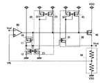
<第一の実施形態>
図1は、第一の実施形態のボルテージレギュレータを示す回路図である。
<First embodiment>
FIG. 1 is a circuit diagram showing a voltage regulator according to the first embodiment.
第一の実施形態のボルテージレギュレータは、センス回路10、制御回路20、制御回路30、出力トランジスタ40、分圧回路50及びアンプ60を備える。
The voltage regulator of the first embodiment includes a
センス回路10は、センストランジスタ11とNMOSトランジスタ12を有する。制御回路20は、PMOSトランジスタ22及び23とNMOSトランジスタ21を有する。制御回路30は、PMOSトランジスタ32及び33とNMOSトランジスタ31を有する。
The
アンプ60の非反転入力端子は分圧回路50の出力端子に接続し、反転入力端子は基準電圧入力端子に接続し、出力端子はセンス回路10の入力端子と制御回路20の出力端子と制御回路30の出力端子と出力トランジスタ40のゲートとに接続する。出力トランジスタ40のソース及びバックゲートは電源端子に接続し、ドレインはボルテージレギュレータの出力端子に接続する。分圧回路50は、ボルテージレギュレータの出力端子と接地端子との間に設けられる。
The non-inverting input terminal of the
センストランジスタ11のゲートはアンプ60の出力端子に接続し、ソース及びバックゲートは電源端子に接続する。NMOSトランジスタ12のゲートはドレインとNMOSトランジスタ21のゲートとNMOSトランジスタ31のゲートとセンストランジスタ11のドレインとに接続し、ソース及びバックゲートは接地端子に接続する。PMOSトランジスタ22のゲートはドレインとPMOSトランジスタ23のゲートとNMOSトランジスタ21のドレインとに接続し、ソース及びバックゲートは電源端子に接続する。PMOSトランジスタ23のソース及びバックゲートは電源端子に接続し、ドレインはアンプ60の出力端子に接続する。NMOSトランジスタ21のソース及びバックゲートは接地端子に接続する。PMOSトランジスタ32のゲートはドレインとPMOSトランジスタ33のゲートとNMOSトランジスタ31のドレインとに接続し、ソース及びバックゲートは電源端子に接続する。PMOSトランジスタ33のソース及びバックゲートは電源端子に接続し、ドレインはアンプ60の出力端子に接続する。NMOSトランジスタ31のソース及びバックゲートはボルテージレギュレータの出力端子に接続する。
The gate of the
PMOSトランジスタ22とPMOSトランジスタ23とはカレントミラー接続する。PMOSトランジスタ32とPMOSトランジスタ33とはカレントミラー接続する。出力トランジスタ40とセンストランジスタ11とはカレントミラー接続する。センストランジスタ11に流れる電流を流すNMOSトランジスタ12とNMOSトランジスタ21とNMOSトランジスタ31とはカレントミラー接続する。
The
分圧回路50は、出力電圧Voutを分圧し、分圧電圧Vfbを出力する。アンプ60は、基準電圧Vrefと分圧電圧Vfbとを比較し、出力電圧Voutが一定になるよう出力トランジスタ40のゲート電圧を制御する。出力トランジスタ40は、アンプ60の出力信号及び電源電圧VDDに基づき、出力電圧Voutを出力する。センス回路10は、センストランジスタ11によって出力トランジスタ40の出力電流Ioutをセンスする。出力電流Ioutが最大出力電流Imになると、制御回路20はNMOSトランジスタ21に流れる電流に基づいて出力トランジスタ40がオフしていくよう動作する。出力電流Ioutが最大出力電流Imになって出力電圧Voutが所定電圧Va以下になると、出力電流Ioutが短絡時出力電流Isになるように、制御回路30はNMOSトランジスタ31に流れる電流に基づいて出力トランジスタ40がさらにオフしていくよう動作する。
The voltage dividing
次に、ボルテージレギュレータの動作について説明する。図2は、ボルテージレギュレータの出力電圧出力電流特性を示す図である。
出力電圧Voutが所定電圧よりも高いと、分圧電圧Vfbが基準電圧Vrefよりも高く、アンプ60の出力信号(出力トランジスタ40のゲート電圧)が高くなり、出力トランジスタ40はオフしていき、出力電圧Voutは低くなる。また、出力電圧Voutが所定電圧よりも低いと、上記と逆の動作をして、出力電圧Voutは高くなる。つまり、出力電圧Voutが一定になる。
Next, the operation of the voltage regulator will be described. FIG. 2 is a diagram illustrating output voltage output current characteristics of the voltage regulator.
When the output voltage Vout is higher than a predetermined voltage, the divided voltage Vfb is higher than the reference voltage Vref, the output signal of the amplifier 60 (the gate voltage of the output transistor 40) becomes high, the
ここで、ボルテージレギュレータの出力端子と接地端子とが短絡すると、出力電流Ioutが増加する。出力電流Ioutが最大出力電流Imになると、最大出力電流Imに応じ、出力トランジスタ40とカレントミラー接続するセンストランジスタ11に流れる電流が多くなり、NMOSトランジスタ12に流れる電流も多くなる。NMOSトランジスタ12とカレントミラー接続するNMOSトランジスタ21に流れる電流も多くなり、PMOSトランジスタ22に流れる電流も多くなる。PMOSトランジスタ22とカレントミラー接続するPMOSトランジスタ23のオン抵抗が低くなり、出力トランジスタ40のゲート・ソース間電圧が低くなり、出力トランジスタ40がオフしていく。よって、出力電流Ioutは最大出力電流Imよりも多く流れず、出力電圧Voutが低くなる。ここで、NMOSトランジスタ21に流れる電流により、出力トランジスタ40のゲート・ソース間電圧が低くなり、出力トランジスタ40がオフしていき、出力電流Ioutが最大出力電流Imに固定されるので、最大出力電流ImはNMOSトランジスタ21に流れる電流によって決定される。
Here, when the output terminal of the voltage regulator and the ground terminal are short-circuited, the output current Iout increases. When the output current Iout becomes the maximum output current Im, according to the maximum output current Im, the current flowing through the
出力電圧Voutが、低くなり、所定電圧Va以下になる。すると、NMOSトランジスタ31のゲート・ソース間電圧が閾値電圧Vtn以上になり、NMOSトランジスタ31はオンする。すると、PMOSトランジスタ32に流れる電流が多くなり、PMOSトランジスタ32とカレントミラー接続するPMOSトランジスタ33のオン抵抗が低くなり、出力トランジスタ40のゲート・ソース間電圧がさらに低くなり、出力トランジスタ40がさらにオフしていく。よって、出力電流Ioutが、少なくなり、短絡時出力電流Isになる。この短絡時出力電流Isは、NMOSトランジスタ31に流れる電流によって決定される。その後、出力電圧Voutが、低くなり、0ボルトになる。ここで、NMOSトランジスタ31に流れる電流により、出力トランジスタ40のゲート・ソース間電圧が低くなり、出力トランジスタ40がオフしていき、出力電流Ioutが短絡時出力電流Isになるので、短絡時出力電流IsはNMOSトランジスタ31に流れる電流によって決定される。
The output voltage Vout becomes low and becomes equal to or lower than the predetermined voltage Va. Then, the gate-source voltage of the
このようにすると、出力トランジスタ40とセンストランジスタ11とはカレントミラー接続し、さらに、センストランジスタ11に流れる電流を流すNMOSトランジスタ12とNMOSトランジスタ21とNMOSトランジスタ31とはカレントミラー接続するので、これらのカレントミラー比に基づき、抵抗の抵抗値のトリミング工程等がなくても、NMOSトランジスタ21及びNMOSトランジスタ31に流れる電流は出力トランジスタ40に流れる出力電流Ioutに対して正確に設定される。つまり、最大出力電流Im及び短絡時出力電流IsがNMOSトランジスタ21及びNMOSトランジスタ31に流れる電流によってそれぞれ決定されるので、最大出力電流Im及び短絡時出力電流Isは出力電流Ioutに対して正確に設定される。
In this way, the
また、制御回路20及び制御回路30に抵抗がないので、その抵抗の抵抗値のトリミング工程もない。よって、そのトリミング工程で使用されるヒューズもなくなるので、ボルテージレギュレータの面積が小さくなる。
Further, since the
なお、図示しないが、PMOSトランジスタ22とPMOSトランジスタ23は、カレントミラー接続する代わりに、PMOSトランジスタ22のゲートに線形領域で動作するような電圧を与える回路に変更しても良い。PMOSトランジスタ32とPMOSトランジスタ33も同様である。
Although not shown, the
また、NMOSトランジスタ31のバックゲートは、図1では、ボルテージレギュレータの出力端子に接続しているが、図示しないが、接地端子に接続しても良い。すると、NMOSトランジスタ31がオンしにくくなり、これに応じ、図2の波形が微調整される。
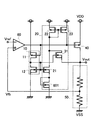
<第二の実施形態>
Further, the back gate of the
<Second Embodiment>
図4は、第二の実施形態のボルテージレギュレータの回路図である。
図1との違いはPMOSトランジスタ22を削除し、PMOSトランジスタ401、402とバイアス電流源403を追加した点である。接続としては、バイアス電流源403は、一方は接地端子に接続され、もう一方はPMOSトランジスタ401のドレインに接続される。PMOSトランジスタ401は、ゲートおよびドレインはPMOSトランジスタ402のゲートに接続され、ソースは電源端子に接続される。PMOSトランジスタ402は、ドレインはPMOSトランジスタ23のゲートおよびNMOSトランジスタ21のドレインに接続され、ソースは電源端子に接続される。
FIG. 4 is a circuit diagram of the voltage regulator according to the second embodiment.
The difference from FIG. 1 is that the
次に第二の実施形態のボルテージレギュレータの動作について説明する。
出力電圧Voutが所定電圧よりも高いと、分圧電圧Vfbが基準電圧Vrefよりも高く、アンプ60の出力信号(出力トランジスタ40のゲート電圧)が高くなり、出力トランジスタ40はオフしていき、出力電圧Voutは低くなる。また、出力電圧Voutが所定電圧よりも低いと、上記と逆の動作をして、出力電圧Voutは高くなる。つまり、出力電圧Voutが一定になる。
Next, the operation of the voltage regulator according to the second embodiment will be described.
When the output voltage Vout is higher than a predetermined voltage, the divided voltage Vfb is higher than the reference voltage Vref, the output signal of the amplifier 60 (the gate voltage of the output transistor 40) becomes high, the
出力電圧が一定である時、バイアス電流源403によってPMOSトランジスタ401に電流が流れる。PMOSトランジスタ401とPMOSトランジスタ402はカレントミラーを構成しているため、PMOSトランジスタ402に電流が流れ、ノード411は電源電圧VDD付近の電圧となる。ノード411が電源電圧VDD付近の電圧のため、PMOSトランジスタ23はオフした状態にある。
When the output voltage is constant, a current flows through the
ここで、ボルテージレギュレータの出力端子と接地端子とが短絡すると、出力電流Ioutが増加する。出力電流Ioutが最大出力電流Imになると、最大出力電流Imに応じ、出力トランジスタ40とカレントミラー接続するセンストランジスタ11に流れる電流が多くなり、NMOSトランジスタ12に流れる電流も多くなる。すると、NMOSトランジスタ12とカレントミラー接続するNMOSトランジスタ21に流れる電流も多くなっていく。ここで、NMOSトランジスタ21に流れる電流がPMOSトランジスタ402に流れる電流より多くなると、ノード411の電圧は電源電圧VDD付近の電圧から接地電圧VSS付近の電圧へと変化していく。ノード411が接地電圧VSS付近の電圧になるとPMOSトランジスタ23がオンしていき、出力トランジスタ40のゲート・ソース間電圧が低くなる。こうして出力トランジスタ40はオフしていく。
Here, when the output terminal of the voltage regulator and the ground terminal are short-circuited, the output current Iout increases. When the output current Iout becomes the maximum output current Im, according to the maximum output current Im, the current flowing through the
出力トランジスタ40とセンストランジスタ11はカレントミラー接続している。さらに、NMOSトランジスタ12とNMOSトランジスタ21はカレントミラー接続している。このためNMOSトランジスタ21に流れる電流は、これらのカレントミラー比に基づき出力電流Ioutに対して正確な比で設定することが可能となる。最大出力電流ImはNMOSトランジスタ21に流れる電流とPMOSトランジスタ402に流れる電流によって決定される。このため、この二つの電流値を調節することで容易に最大出力電流Imを調節することが可能となる。
The
以上記載したように、第二の実施形態のボルテージレギュレータは、最大出力電流ImをNMOSトランジスタ21に流れる電流とPMOSトランジスタ402に流れる電流によって容易に設定および調節することが可能となる。
<第三の実施形態>
As described above, in the voltage regulator according to the second embodiment, the maximum output current Im can be easily set and adjusted by the current flowing through the
<Third embodiment>
図5は、第三の実施形態のボルテージレギュレータの回路図である。
図1との違いはPMOSトランジスタ32、33、NMOSトランジスタ12を削除し、NLトランジスタ501を追加した点である。接続としては、NLトランジスタ501は、ゲートおよびドレインはNMOSトランジスタ21のゲートおよびNMOSトランジスタ31のゲートに接続され、ソースは接地端子に接続される。NMOSトランジスタ31は、ドレインはNMOSトランジスタ21のドレインとPMOSトランジスタ22のドレインおよびゲートに接続され、ソースは出力端子に接続される。
FIG. 5 is a circuit diagram of a voltage regulator according to the third embodiment.
The difference from FIG. 1 is that the
次に第三の実施形態のボルテージレギュレータの動作について説明する。NLトランジスタとはNMOSトランジスタと比べて閾値の低いトランジスタの事を指す。
出力電圧Voutが所定電圧よりも高いと、分圧電圧Vfbが基準電圧Vrefよりも高く、アンプ60の出力信号(出力トランジスタ40のゲート電圧)が高くなり、出力トランジスタ40はオフしていき、出力電圧Voutは低くなる。また、出力電圧Voutが所定電圧よりも低いと、上記と逆の動作をして、出力電圧Voutは高くなる。つまり、出力電圧Voutが一定になる。
Next, the operation of the voltage regulator of the third embodiment will be described. An NL transistor refers to a transistor having a lower threshold value than an NMOS transistor.
When the output voltage Vout is higher than a predetermined voltage, the divided voltage Vfb is higher than the reference voltage Vref, the output signal of the amplifier 60 (the gate voltage of the output transistor 40) becomes high, the
ここで、ボルテージレギュレータの出力端子と接地端子とが短絡すると、出力電流Ioutが増加する。出力電流Ioutが最大出力電流Imになると、最大出力電流Imに応じ、出力トランジスタ40とカレントミラー接続するセンストランジスタ11に流れる電流が多くなる。するとNLトランジスタ501に流れる電流も多くなり、カレントミラー接続するNMOSトランジスタ21に流れる電流も多くなっていく。NMOSトランジスタ21に電流が流れるとPMOSトランジスタ22にも電流が流れ、カレントミラー接続するPMOSトランジスタ23にも電流が流れていく。こうして出力トランジスタ40のゲート・ソース間電圧が低くなり、出力トランジスタ40はオフしていく。最大出力電流ImはNMOSトランジスタ21に流れる電流によって決定される。
Here, when the output terminal of the voltage regulator and the ground terminal are short-circuited, the output current Iout increases. When the output current Iout becomes the maximum output current Im, the current flowing through the
出力電圧Voutが低くなり所定電圧Va以下になる。すると、NMOSトランジスタ31のゲート・ソース間電圧が閾値電圧Vtn以上になり、NMOSトランジスタ31はオンする。すると、PMOSトランジスタ22に流れる電流が多くなり、PMOSトランジスタ22とカレントミラー接続するPMOSトランジスタ23のオン抵抗が低くなる。こうして出力トランジスタ40のゲート・ソース間電圧がさらに低くなり、出力トランジスタ40がさらにオフしていく。出力トランジスタ40がさらにオフすると出力電流Ioutが少なくなり、短絡時出力電流Isまで制限される。この短絡時出力電流Isは、NMOSトランジスタ31に流れる電流によって決定することができる。その後、出力電圧Voutはさらに低くなり0ボルトになっていく。
The output voltage Vout decreases and becomes equal to or lower than the predetermined voltage Va. Then, the gate-source voltage of the
出力トランジスタ40とセンストランジスタ11はカレントミラー接続している。さらに、NLトランジスタ501とNMOSトランジスタ21とNMOSトランジスタ31はカレントミラー接続している。このためNMOSトランジスタ21およびNMOSトランジスタ31に流れる電流は、これらのカレントミラー比に基づき出力電流Ioutに対して正確な比で設定することが可能となる。最大出力電流Im及び短絡時出力電流IsはNMOSトランジスタ21及びNMOSトランジスタ31に流れる電流によって決定される。このため、最大出力電流Im及び短絡時出力電流Isは出力電流Ioutに対して正確な比で設定することが可能となる。
The
また、PMOSトランジスタ32、33を削除しているため、さらにボルテージレギュレータの面積を小さくなすることができる。
Further, since the
NLトランジスタ501は、出力電流Ioutが最大出力電流Imになる前に出力電圧が低下するのを防止するために用いている。出力端子と接地端子とが短絡し出力電流Ioutが上昇するとセンストランジスタ11で電流をセンスして、出力トランジスタ40をオフしていく。この時、最大出力電流Im以下であってもセンストランジスタ11は電流を正確に検出し、PMOSトランジスタ23に電流を流していく。このため、図7の点線で示すように、最大出力電流Imに達する前に出力トランジスタ40をオフさせる動作が開始し、出力電圧が低下してしまうのである。これを防ぐために、NLトランジスタ501とNMOSトランジスタ21の閾値に差を設けることでミラー比をずらし、最大出力電流Im以下では動作しないようにしている。
The
なお、図示はしないがNLトランジスタ501はNMOSトランジスタを用いても良い。
以上記載したように、第三の実施形態のボルテージレギュレータは、最大出力電流Im及び短絡時出力電流IsをNMOSトランジスタ21及びNMOSトランジスタ31に流れる電流によって設定および調節することが可能となる。また、トランジスタ数を減らすためさらに小さい面積で実現することが可能となる。
<第四の実施形態>
Although not shown, the
As described above, the voltage regulator according to the third embodiment can set and adjust the maximum output current Im and the short-circuit output current Is by the currents flowing through the
<Fourth embodiment>
図6は、第四の実施形態のボルテージレギュレータの回路図である。
図1との違いはPMOSトランジスタ32、33を削除し、NMOSトランジスタ601を追加した点である。接続としては、NMOSトランジスタ601は、ゲートおよびドレインはNMOSトランジスタ21のソースに接続され、ソースは接地端子に接続される。
FIG. 6 is a circuit diagram of a voltage regulator according to the fourth embodiment.
The difference from FIG. 1 is that the
次に第四の実施形態のボルテージレギュレータの動作について説明する。
NMOSトランジスタ21のソースにNMOSトランジスタ601を追加することでNMOSトランジスタ12とNMOSトランジスタ21のミラー比をずらすことができる。このミラー比をずらすことによって最大出力電流Im以下で出力電圧が低下するのを防止することができる。また、NLトランジスタを用いないためNLトランジスタ用のマスクや工程を省くことができ、製造コスト削減を行うことができる。
Next, the operation of the voltage regulator of the fourth embodiment will be described.
By adding the
また、図示はしないがさらにミラー比をずらすためNMOSトランジスタ12にNLトランジスタを用いても良い。
Although not shown, an NL transistor may be used as the
以上記載したように、第四の実施形態のボルテージレギュレータは、最大出力電流Im及び短絡時出力電流IsをNMOSトランジスタ21及びNMOSトランジスタ31に流れる電流によって設定および調節することが可能となる。また、NLトランジスタを用いずにNMOSトランジスタ12とNMOSトランジスタ21のミラー比をずらすため、製造コスト削減を行うことができる。
As described above, the voltage regulator according to the fourth embodiment can set and adjust the maximum output current Im and the short-circuit output current Is by the currents flowing through the
10 センス回路
20、30 制御回路
40 出力トランジスタ
50 分圧回路
60 アンプ
403 バイアス電流源
501 NLトランジスタ
10
Claims (10)
前記出力トランジスタとカレントミラー接続し、前記出力トランジスタの出力電流をセンスするセンストランジスタと、
前記センストランジスタに流れる電流を流す第一トランジスタと、
ソースが接地端子に接続され、前記第一トランジスタとカレントミラー接続する第二トランジスタと、電源端子と前記第二トランジスタのドレインとの間に設けられ、順方向にダイオード接続する第三トランジスタと、前記第三トランジスタとカレントミラー接続し、ドレインを前記出力トランジスタのゲートに接続する第四トランジスタと、を有し、前記出力電流が最大出力電流になると、前記第二トランジスタに流れる電流に基づいて前記出力トランジスタがオフしていくよう制御する第一制御回路と、
ソースが前記出力端子に接続され、前記第一トランジスタとカレントミラー接続する第五トランジスタと、前記電源端子と前記第五トランジスタのドレインとの間に設けられ、順方向にダイオード接続する第六トランジスタと、前記第六トランジスタとカレントミラー接続し、ドレインを前記出力トランジスタのゲートに接続する第七トランジスタと、を有し、前記出力電流が前記最大出力電流になり、且つ前記出力電圧が所定電圧以下になると、前記出力電流が短絡時出力電流になるように、前記第五トランジスタに流れる電流に基づいて前記出力トランジスタがさらにオフしていくよう制御する第二制御回路と、を備える、
ことを特徴とするボルテージレギュレータ。 A voltage regulator including an amplifier that amplifies a difference between a reference voltage and a voltage based on an output voltage and controls a gate voltage of an output transistor so that an output voltage of an output terminal becomes constant,
A sense transistor that is current mirror connected to the output transistor and senses an output current of the output transistor;
A first transistor for passing a current flowing through the sense transistor;
A source connected to a ground terminal, a second transistor connected to the first transistor in a current mirror connection, a third transistor provided between a power supply terminal and the drain of the second transistor, and diode-connected in a forward direction; A fourth transistor having a current mirror connection with a third transistor and a drain connected to the gate of the output transistor, and when the output current reaches a maximum output current, the output is based on the current flowing through the second transistor. A first control circuit for controlling the transistor to turn off;
A fifth transistor having a source connected to the output terminal and connected to the first transistor in a current mirror connection; a sixth transistor provided between the power supply terminal and the drain of the fifth transistor and diode-connected in a forward direction; A seventh transistor having a current mirror connection with the sixth transistor and a drain connected to the gate of the output transistor , wherein the output current becomes the maximum output current, and the output voltage is equal to or lower than a predetermined voltage. A second control circuit that controls the output transistor to be further turned off based on a current flowing through the fifth transistor so that the output current becomes an output current at the time of a short circuit,
This is a voltage regulator.
前記出力トランジスタとカレントミラー接続し、前記出力トランジスタの出力電流をセンスするセンストランジスタと、
前記センストランジスタに流れる電流を流す第一トランジスタと、
ソースが接地端子に接続され、前記第一トランジスタとカレントミラー接続する第二トランジスタと、電源端子と前記第二トランジスタのドレインとの間に設けられ、ゲートに線形領域で動作する電圧が印加される第三トランジスタと、ゲートを前記第三トランジスタのドレインと接続し、ソースを前記電源端子と接続し、ドレインを前記出力トランジスタのゲートに接続する第四トランジスタと、を有し、前記出力電流が最大出力電流になると、前記第二トランジスタに流れる電流に基づいて前記出力トランジスタがオフしていくよう制御する第一制御回路と、
ソースが前記出力端子に接続され、前記第一トランジスタとカレントミラー接続する第五トランジスタと、前記電源端子と前記第五トランジスタのドレインとの間に設けられ、順方向にダイオード接続する第六トランジスタと、前記第六トランジスタとカレントミラー接続し、ドレインを前記出力トランジスタのゲートに接続する第七トランジスタと、を有し、前記出力電流が前記最大出力電流になり、且つ前記出力電圧が所定電圧以下になると、前記出力電流が短絡時出力電流になるように、前記第五トランジスタに流れる電流に基づいて前記出力トランジスタがさらにオフしていくよう制御する第二制御回路と、を備える、
ことを特徴とするボルテージレギュレータ。 A voltage regulator including an amplifier that amplifies a difference between a reference voltage and a voltage based on an output voltage and controls a gate voltage of an output transistor so that an output voltage of an output terminal becomes constant,
A sense transistor that is current mirror connected to the output transistor and senses an output current of the output transistor;
A first transistor for passing a current flowing through the sense transistor;
A source is connected to the ground terminal, a second transistor that is connected to the first transistor in a current mirror connection , a power supply terminal and a drain of the second transistor, and a voltage that operates in a linear region is applied to the gate. A fourth transistor having a third transistor, a gate connected to the drain of the third transistor, a source connected to the power supply terminal, and a drain connected to the gate of the output transistor , wherein the output current is maximum When the output current is reached, a first control circuit that controls the output transistor to turn off based on the current flowing through the second transistor;
A fifth transistor having a source connected to the output terminal and connected to the first transistor in a current mirror connection; a sixth transistor provided between the power supply terminal and the drain of the fifth transistor and diode-connected in a forward direction; A seventh transistor having a current mirror connection with the sixth transistor and a drain connected to the gate of the output transistor , wherein the output current becomes the maximum output current, and the output voltage is equal to or lower than a predetermined voltage. A second control circuit that controls the output transistor to be further turned off based on a current flowing through the fifth transistor so that the output current becomes an output current at the time of a short circuit,
This is a voltage regulator.
一方の端子を前記接地端子に接続されるバイアス電流源と
前記電源端子と前記バイアス電流源の他方の端子との間に設けられ、順方向にダイオード接続し、前記第三トランジスタとカレントミラー接続する第八トランジスタと、を備えた
ことを特徴とする請求項2記載のボルテージレギュレータ。 The first control circuit includes:
One terminal is provided between the bias current source connected to the ground terminal, the power supply terminal and the other terminal of the bias current source, diode-connected in the forward direction, and current mirror connected to the third transistor The voltage regulator according to claim 2 , further comprising an eighth transistor.
前記出力トランジスタとカレントミラー接続し、前記出力トランジスタの出力電流をセンスするセンストランジスタと、
前記センストランジスタに流れる電流を流す第一トランジスタと、
前記第一トランジスタとカレントミラー接続し、ソースを接地端子に接続する第二トランジスタと、
電源端子と前記第二トランジスタのドレインとの間に設けられ、順方向にダイオード接続する第三トランジスタと、
前記第三トランジスタとカレントミラー接続し、ドレインを前記出力トランジスタのゲートに接続する第四トランジスタと、
前記第一トランジスタとカレントミラー接続し、ドレインを前記第二トランジスタのドレインに接続し、ソースを前記出力端子に接続する第五トランジスタと、を有し、
前記出力電流が最大出力電流になると、前記第二トランジスタに流れる電流に基づいて前記出力トランジスタがオフしていくよう制御し、
前記出力電流が前記最大出力電流になり、且つ前記出力電圧が所定電圧以下になると、前記出力電流が短絡時出力電流になるように、前記第五トランジスタに流れる電流に基づいて前記出力トランジスタがさらにオフしていくよう制御する制御回路と、を備える、
ことを特徴とするボルテージレギュレータ。 A voltage regulator including an amplifier that amplifies a difference between a reference voltage and a voltage based on an output voltage and controls a gate voltage of an output transistor so that an output voltage of an output terminal becomes constant,
A sense transistor that is current mirror connected to the output transistor and senses an output current of the output transistor;
A first transistor for passing a current flowing through the sense transistor;
A second mirror for connecting the first transistor to a ground terminal in a current mirror connection;
A third transistor provided between the power supply terminal and the drain of the second transistor and diode-connected in the forward direction;
A fourth transistor that is current mirror connected to the third transistor and has a drain connected to the gate of the output transistor;
A fifth mirror having a current mirror connection with the first transistor, a drain connected to the drain of the second transistor, and a source connected to the output terminal;
When the output current reaches the maximum output current, the output transistor is controlled to turn off based on the current flowing through the second transistor,
When the output current becomes the maximum output current and the output voltage becomes a predetermined voltage or less, the output transistor further includes a current flowing through the fifth transistor so that the output current becomes an output current at the time of a short circuit. A control circuit for controlling to turn off,
This is a voltage regulator.
ことを特徴とする請求項4記載のボルテージレギュレータ。 The first transistor is composed of a transistor having a lower threshold than other transistors.
The voltage regulator according to claim 4 .
ことを特徴とする請求項4または5記載のボルテージレギュレータ。 A sixth transistor that is diode-connected in a forward direction between the ground terminal and the second transistor;
The voltage regulator according to claim 4 or 5, wherein
前記出力トランジスタとカレントミラー接続し、前記出力トランジスタの出力電流をセンスするセンストランジスタと、
前記センストランジスタに流れる電流を流す第一トランジスタと、
ソースが接地端子に接続され、前記第一トランジスタとカレントミラー接続する第二トランジスタと、電源端子と前記第二トランジスタのドレインとの間に設けられ、順方向にダイオード接続する第三トランジスタと、前記第三トランジスタとカレントミラー接続し、ドレインを前記出力トランジスタのゲートに接続する第四トランジスタと、を有し、前記出力電流が最大出力電流になると、前記第二トランジスタに流れる電流に基づいて前記出力トランジスタがオフしていくよう制御する第一制御回路と、
ソースが前記出力端子に接続され、前記第一トランジスタとカレントミラー接続する第五トランジスタと、前記電源端子と前記第五トランジスタのドレインとの間に設けられ、ゲートに線形領域で動作する電圧が印加される第六トランジスタと、前記第六トランジスタとカレントミラー接続し、ドレインを前記出力トランジスタのゲートに接続する第七トランジスタと、を有し、前記出力電流が前記最大出力電流になり、且つ前記出力電圧が所定電圧以下になると、前記出力電流が短絡時出力電流になるように、前記第五トランジスタに流れる電流に基づいて前記出力トランジスタがさらにオフしていくよう制御する第二制御回路と、を備える、
ことを特徴とするボルテージレギュレータ。 A voltage regulator including an amplifier that amplifies a difference between a reference voltage and a voltage based on an output voltage and controls a gate voltage of an output transistor so that an output voltage of an output terminal becomes constant,
A sense transistor that is current mirror connected to the output transistor and senses an output current of the output transistor;
A first transistor for passing a current flowing through the sense transistor;
A source connected to a ground terminal, a second transistor connected to the first transistor in a current mirror connection, a third transistor provided between a power supply terminal and the drain of the second transistor, and diode-connected in a forward direction; A fourth transistor having a current mirror connection with a third transistor and a drain connected to the gate of the output transistor, and when the output current reaches a maximum output current, the output is based on the current flowing through the second transistor. A first control circuit for controlling the transistor to turn off;
A source is connected to the output terminal, a fifth transistor that is current-mirror connected to the first transistor, and a voltage that operates between the power supply terminal and the drain of the fifth transistor and operates in a linear region is applied to the gate. A sixth transistor connected to the sixth transistor in a current mirror connection and having a drain connected to the gate of the output transistor , the output current being the maximum output current, and the output A second control circuit for controlling the output transistor to be further turned off based on a current flowing through the fifth transistor so that the output current becomes an output current when short-circuited when the voltage becomes equal to or lower than a predetermined voltage; Prepare
This is a voltage regulator.
一方の端子を前記接地端子に接続されるバイアス電流源と、
前記電源端子と前記バイアス電流源の他方の端子との間に設けられ、順方向にダイオード接続し、前記第六トランジスタとカレントミラー接続する第八トランジスタと、を備えた、
ことを特徴とする請求項7記載のボルテージレギュレータ。 The second control circuit includes:
A bias current source having one terminal connected to the ground terminal;
An eighth transistor provided between the power supply terminal and the other terminal of the bias current source, diode-connected in the forward direction, and connected to the sixth transistor and a current mirror;
The voltage regulator according to claim 7 .
前記出力トランジスタとカレントミラー接続し、前記出力トランジスタの出力電流をセンスするセンストランジスタと、
前記センストランジスタに流れる電流を流す第一トランジスタと、
ソースが接地端子に接続され、前記第一トランジスタとカレントミラー接続する第二トランジスタと、電源端子と前記第二トランジスタのドレインとの間に設けられ、ゲートに線形領域で動作する電圧が印加される第三トランジスタと、
ゲートを前記第三トランジスタのドレインと接続し、ソースを前記電源端子と接続し、ドレインを前記出力トランジスタのゲートに接続する第四トランジスタと、を有し、前記出力電流が最大出力電流になると、前記第二トランジスタに流れる電流に基づいて前記出力トランジスタがオフしていくよう制御する第一制御回路と、
ソースが前記出力端子に接続され、前記第一トランジスタとカレントミラー接続する第五トランジスタと、前記電源端子と前記第五トランジスタのドレインとの間に設けられ、ゲートに線形領域で動作する電圧が印加される第六トランジスタと、前記第六トランジスタとカレントミラー接続し、ドレインを前記出力トランジスタのゲートに接続する第七トランジスタと、を有し、前記出力電流が前記最大出力電流になり、且つ前記出力電圧が所定電圧以下になると、前記出力電流が短絡時出力電流になるように、前記第五トランジスタに流れる電流に基づいて前記出力トランジスタがさらにオフしていくよう制御する第二制御回路と、を備える、
ことを特徴とするボルテージレギュレータ。 A voltage regulator including an amplifier that amplifies a difference between a reference voltage and a voltage based on an output voltage and controls a gate voltage of an output transistor so that an output voltage of an output terminal becomes constant,
A sense transistor that is current mirror connected to the output transistor and senses an output current of the output transistor;
A first transistor for passing a current flowing through the sense transistor;
A source is connected to the ground terminal, a second transistor that is connected to the first transistor in a current mirror connection , a power supply terminal and a drain of the second transistor, and a voltage that operates in a linear region is applied to the gate. A third transistor;
A fourth transistor that has a gate connected to the drain of the third transistor, a source connected to the power supply terminal, and a drain connected to the gate of the output transistor, and when the output current becomes a maximum output current, A first control circuit for controlling the output transistor to turn off based on a current flowing through the second transistor;
A source is connected to the output terminal, a fifth transistor that is current-mirror connected to the first transistor, and a voltage that operates between the power supply terminal and the drain of the fifth transistor and operates in a linear region is applied to the gate. A sixth transistor connected to the sixth transistor in a current mirror connection and having a drain connected to the gate of the output transistor , the output current being the maximum output current, and the output A second control circuit for controlling the output transistor to be further turned off based on a current flowing through the fifth transistor so that the output current becomes an output current when short-circuited when the voltage becomes equal to or lower than a predetermined voltage; Prepare
This is a voltage regulator.
一方の端子を前記接地端子に接続されるバイアス電流源と
前記電源端子と前記バイアス電流源の他方の端子との間に設けられ、順方向にダイオード接続し、前記第三トランジスタとカレントミラー接続する第八トランジスタと、を備えた
前記第二制御回路は、
一方の端子を前記接地端子に接続されるバイアス電流源と
前記電源端子と前記バイアス電流源の他方の端子との間に設けられ、順方向にダイオード接続し、前記第六トランジスタとカレントミラー接続する第九トランジスタと、を備えた
ことを特徴とする請求項9記載のボルテージレギュレータ。 The first control circuit includes:
One terminal is provided between the bias current source connected to the ground terminal, the power supply terminal and the other terminal of the bias current source, diode-connected in the forward direction, and current mirror connected to the third transistor The second control circuit comprising an eighth transistor,
One terminal is provided between the bias current source connected to the ground terminal, the power supply terminal and the other terminal of the bias current source, diode-connected in the forward direction, and current mirror connected to the sixth transistor The voltage regulator according to claim 9 , further comprising a ninth transistor.
Priority Applications (5)
| Application Number | Priority Date | Filing Date | Title |
|---|---|---|---|
| JP2010007380A JP5580608B2 (en) | 2009-02-23 | 2010-01-15 | Voltage regulator |
| TW099103851A TWI489239B (en) | 2009-02-23 | 2010-02-08 | Voltage regulator |
| KR1020100015119A KR101435238B1 (en) | 2009-02-23 | 2010-02-19 | Voltage regulator |
| US12/709,784 US8384370B2 (en) | 2009-02-23 | 2010-02-22 | Voltage regulator with an overcurrent protection circuit |
| CN201010118220.6A CN101813957B (en) | 2009-02-23 | 2010-02-23 | Voltage regulator |
Applications Claiming Priority (3)
| Application Number | Priority Date | Filing Date | Title |
|---|---|---|---|
| JP2009039340 | 2009-02-23 | ||
| JP2009039340 | 2009-02-23 | ||
| JP2010007380A JP5580608B2 (en) | 2009-02-23 | 2010-01-15 | Voltage regulator |
Publications (3)
| Publication Number | Publication Date |
|---|---|
| JP2010218543A JP2010218543A (en) | 2010-09-30 |
| JP2010218543A5 JP2010218543A5 (en) | 2012-12-27 |
| JP5580608B2 true JP5580608B2 (en) | 2014-08-27 |
Family
ID=42621231
Family Applications (1)
| Application Number | Title | Priority Date | Filing Date |
|---|---|---|---|
| JP2010007380A Active JP5580608B2 (en) | 2009-02-23 | 2010-01-15 | Voltage regulator |
Country Status (5)
| Country | Link |
|---|---|
| US (1) | US8384370B2 (en) |
| JP (1) | JP5580608B2 (en) |
| KR (1) | KR101435238B1 (en) |
| CN (1) | CN101813957B (en) |
| TW (1) | TWI489239B (en) |
Families Citing this family (30)
| Publication number | Priority date | Publication date | Assignee | Title |
|---|---|---|---|---|
| KR101090032B1 (en) * | 2010-02-08 | 2011-12-05 | 삼성전기주식회사 | Power-source control system and power amplifying system using the same |
| TWI427455B (en) * | 2011-01-04 | 2014-02-21 | Faraday Tech Corp | Voltage regulator |
| CN102594145B (en) * | 2011-01-14 | 2014-08-20 | 智原科技股份有限公司 | Voltage regulator |
| JP5670773B2 (en) | 2011-02-01 | 2015-02-18 | セイコーインスツル株式会社 | Voltage regulator |
| JP5676340B2 (en) * | 2011-03-30 | 2015-02-25 | セイコーインスツル株式会社 | Voltage regulator |
| JP5823717B2 (en) * | 2011-03-30 | 2015-11-25 | セイコーインスツル株式会社 | Voltage regulator |
| KR101843433B1 (en) * | 2011-04-04 | 2018-05-15 | 삼성전자주식회사 | Circuit for regulating voltage, contactless card, and contactless card system comprising the same |
| JP5806853B2 (en) * | 2011-05-12 | 2015-11-10 | セイコーインスツル株式会社 | Voltage regulator |
| JP5715525B2 (en) * | 2011-08-05 | 2015-05-07 | セイコーインスツル株式会社 | Voltage regulator |
| TWI457742B (en) * | 2011-11-01 | 2014-10-21 | Faraday Tech Corp | Voltage regulator and operating method thereof |
| JP2013130937A (en) * | 2011-12-20 | 2013-07-04 | Ricoh Co Ltd | Constant voltage circuit and electronic equipment |
| JP5950591B2 (en) * | 2012-01-31 | 2016-07-13 | エスアイアイ・セミコンダクタ株式会社 | Voltage regulator |
| US8773096B2 (en) | 2012-03-29 | 2014-07-08 | Integrated Device Technology, Inc. | Apparatuses and methods responsive to output variations in voltage regulators |
| CN103383580B (en) * | 2012-05-03 | 2015-07-15 | 三星半导体(中国)研究开发有限公司 | Self-adaptive low drop regulator |
| JP6030879B2 (en) * | 2012-07-26 | 2016-11-24 | エスアイアイ・セミコンダクタ株式会社 | Voltage regulator |
| US9058049B2 (en) * | 2012-09-11 | 2015-06-16 | St-Ericsson Sa | Modular low-power unit with analog synchronization loop usable with a low-dropout regulator |
| EP2713492B1 (en) * | 2012-09-26 | 2019-11-27 | ams AG | Power Conversion Arrangement and Method for Power Conversion |
| TWI503644B (en) * | 2012-10-05 | 2015-10-11 | Faraday Tech Corp | Calibration circuit for a voltage regulator |
| JP2014164702A (en) * | 2013-02-27 | 2014-09-08 | Seiko Instruments Inc | Voltage regulator |
| JP6342240B2 (en) * | 2013-08-26 | 2018-06-13 | エイブリック株式会社 | Voltage regulator |
| KR20150050880A (en) * | 2013-11-01 | 2015-05-11 | 에스케이하이닉스 주식회사 | Voltage regulator and apparatus for controlling bias current |
| JP6294061B2 (en) * | 2013-11-29 | 2018-03-14 | ローム株式会社 | Short circuit protection circuit |
| JP6292859B2 (en) * | 2013-12-17 | 2018-03-14 | エイブリック株式会社 | Voltage regulator |
| JP6316632B2 (en) * | 2014-03-25 | 2018-04-25 | エイブリック株式会社 | Voltage regulator |
| JP6253481B2 (en) * | 2014-03-27 | 2017-12-27 | エスアイアイ・セミコンダクタ株式会社 | Voltage regulator and manufacturing method thereof |
| JP6316647B2 (en) * | 2014-04-25 | 2018-04-25 | エイブリック株式会社 | Overcurrent protection circuit, semiconductor device, and voltage regulator |
| CN110018708A (en) * | 2018-01-10 | 2019-07-16 | 圣邦微电子(北京)股份有限公司 | A kind of reliable current-limiting circuit based on current operator |
| EP3660473B1 (en) * | 2018-11-30 | 2024-09-18 | STMicroelectronics (Research & Development) Limited | Apparatus and method for controlling the voltage applied to a single photon avalanche photodiode (spad) |
| US11217992B2 (en) | 2019-09-20 | 2022-01-04 | Texas Instruments Incorporated | High-speed short-to-ground protection circuit for pass field-effect transistor (FET) |
| CN116366046B (en) * | 2022-12-30 | 2024-04-05 | 深圳市芯波微电子有限公司 | Field effect transistor control circuit and electronic equipment |
Family Cites Families (17)
| Publication number | Priority date | Publication date | Assignee | Title |
|---|---|---|---|---|
| US5745000A (en) * | 1996-08-19 | 1998-04-28 | International Business Machines Incorporated | CMOS low voltage current reference |
| CN1193283C (en) * | 2001-01-02 | 2005-03-16 | 深圳赛意法微电子有限公司 | Current-limiting protection circuit for voltage stabilizer |
| JP4574902B2 (en) * | 2001-07-13 | 2010-11-04 | セイコーインスツル株式会社 | Voltage regulator |
| JP2003216252A (en) * | 2001-11-15 | 2003-07-31 | Seiko Instruments Inc | Voltage regulator |
| JP3782726B2 (en) * | 2001-12-13 | 2006-06-07 | 株式会社リコー | Overcurrent protection circuit |
| JP2004118411A (en) * | 2002-09-25 | 2004-04-15 | Seiko Instruments Inc | Voltage regulator |
| US6744242B1 (en) * | 2003-01-14 | 2004-06-01 | Fujitsu Limited | Four-state switched decoupling capacitor system for active power stabilizer |
| JP4421909B2 (en) * | 2004-01-28 | 2010-02-24 | セイコーインスツル株式会社 | Voltage regulator |
| JP4082355B2 (en) * | 2004-01-30 | 2008-04-30 | ミツミ電機株式会社 | Current limit circuit |
| JP2005235932A (en) * | 2004-02-18 | 2005-09-02 | Seiko Instruments Inc | Voltage regulator and method of manufacturing the same |
| US7362079B1 (en) * | 2004-03-03 | 2008-04-22 | Cypress Semiconductor Corporation | Voltage regulator circuit |
| JP4552569B2 (en) * | 2004-09-13 | 2010-09-29 | ソニー株式会社 | Constant voltage power circuit |
| JP2006139673A (en) * | 2004-11-15 | 2006-06-01 | Seiko Instruments Inc | Voltage regulator |
| JP2008026947A (en) * | 2006-07-18 | 2008-02-07 | Seiko Instruments Inc | Voltage regulator |
| TW200836037A (en) * | 2006-12-08 | 2008-09-01 | Seiko Instr Inc | Voltage regulator |
| US7498780B2 (en) * | 2007-04-24 | 2009-03-03 | Mediatek Inc. | Linear voltage regulating circuit with undershoot minimization and method thereof |
| JP5008472B2 (en) * | 2007-06-21 | 2012-08-22 | セイコーインスツル株式会社 | Voltage regulator |
-
2010
- 2010-01-15 JP JP2010007380A patent/JP5580608B2/en active Active
- 2010-02-08 TW TW099103851A patent/TWI489239B/en active
- 2010-02-19 KR KR1020100015119A patent/KR101435238B1/en active IP Right Grant
- 2010-02-22 US US12/709,784 patent/US8384370B2/en active Active
- 2010-02-23 CN CN201010118220.6A patent/CN101813957B/en active Active
Also Published As
| Publication number | Publication date |
|---|---|
| KR101435238B1 (en) | 2014-08-28 |
| KR20100096014A (en) | 2010-09-01 |
| US20100213909A1 (en) | 2010-08-26 |
| TW201042413A (en) | 2010-12-01 |
| JP2010218543A (en) | 2010-09-30 |
| CN101813957A (en) | 2010-08-25 |
| CN101813957B (en) | 2014-04-09 |
| TWI489239B (en) | 2015-06-21 |
| US8384370B2 (en) | 2013-02-26 |
Similar Documents
| Publication | Publication Date | Title |
|---|---|---|
| JP5580608B2 (en) | Voltage regulator | |
| US8450986B2 (en) | Voltage regulator | |
| JP5008472B2 (en) | Voltage regulator | |
| US7852054B2 (en) | Low dropout regulator and the over current protection circuit thereof | |
| US9298200B2 (en) | Constant voltage circuit with drooping and foldback overcurrent protection | |
| JP6506133B2 (en) | Voltage regulator | |
| KR101586525B1 (en) | Voltage regulator | |
| US8665020B2 (en) | Differential amplifier circuit that can change current flowing through a constant-current source according to load variation, and series regulator including the same | |
| US8742819B2 (en) | Current limiting circuitry and method for pass elements and output stages | |
| US9348350B2 (en) | Voltage regulator | |
| US20120242312A1 (en) | Voltage regulator | |
| US9411345B2 (en) | Voltage regulator | |
| JP5279544B2 (en) | Voltage regulator | |
| JP2008052516A (en) | Constant voltage circuit | |
| JP4996203B2 (en) | Power supply voltage circuit | |
| JP6498503B2 (en) | Current detection circuit | |
| US10505438B2 (en) | Overcurrent protection circuit and voltage regulator | |
| JP4555131B2 (en) | Constant voltage power circuit | |
| JP4892366B2 (en) | Overcurrent protection circuit and voltage regulator | |
| US10094857B2 (en) | Current detection circuit | |
| US9588540B2 (en) | Supply-side voltage regulator | |
| US20100060249A1 (en) | Current-restriction circuit and driving method therefor | |
| KR102658159B1 (en) | Overheat protection circuit and semiconductor apparatus having the same |
Legal Events
| Date | Code | Title | Description |
|---|---|---|---|
| A521 | Request for written amendment filed |
Free format text: JAPANESE INTERMEDIATE CODE: A523 Effective date: 20121109 |
|
| A621 | Written request for application examination |
Free format text: JAPANESE INTERMEDIATE CODE: A621 Effective date: 20121109 |
|
| A977 | Report on retrieval |
Free format text: JAPANESE INTERMEDIATE CODE: A971007 Effective date: 20131010 |
|
| A131 | Notification of reasons for refusal |
Free format text: JAPANESE INTERMEDIATE CODE: A131 Effective date: 20131022 |
|
| A521 | Request for written amendment filed |
Free format text: JAPANESE INTERMEDIATE CODE: A523 Effective date: 20131219 |
|
| A131 | Notification of reasons for refusal |
Free format text: JAPANESE INTERMEDIATE CODE: A131 Effective date: 20140415 |
|
| A521 | Request for written amendment filed |
Free format text: JAPANESE INTERMEDIATE CODE: A523 Effective date: 20140610 |
|
| TRDD | Decision of grant or rejection written | ||
| A01 | Written decision to grant a patent or to grant a registration (utility model) |
Free format text: JAPANESE INTERMEDIATE CODE: A01 Effective date: 20140701 |
|
| A61 | First payment of annual fees (during grant procedure) |
Free format text: JAPANESE INTERMEDIATE CODE: A61 Effective date: 20140711 |
|
| R150 | Certificate of patent or registration of utility model |
Ref document number: 5580608 Country of ref document: JP Free format text: JAPANESE INTERMEDIATE CODE: R150 |
|
| S111 | Request for change of ownership or part of ownership |
Free format text: JAPANESE INTERMEDIATE CODE: R313113 |
|
| R350 | Written notification of registration of transfer |
Free format text: JAPANESE INTERMEDIATE CODE: R350 |
|
| R250 | Receipt of annual fees |
Free format text: JAPANESE INTERMEDIATE CODE: R250 |
|
| S533 | Written request for registration of change of name |
Free format text: JAPANESE INTERMEDIATE CODE: R313533 |
|
| R350 | Written notification of registration of transfer |
Free format text: JAPANESE INTERMEDIATE CODE: R350 |
|
| R250 | Receipt of annual fees |
Free format text: JAPANESE INTERMEDIATE CODE: R250 |
|
| R250 | Receipt of annual fees |
Free format text: JAPANESE INTERMEDIATE CODE: R250 |
|
| R250 | Receipt of annual fees |
Free format text: JAPANESE INTERMEDIATE CODE: R250 |
|
| R250 | Receipt of annual fees |
Free format text: JAPANESE INTERMEDIATE CODE: R250 |
|
| S531 | Written request for registration of change of domicile |
Free format text: JAPANESE INTERMEDIATE CODE: R313531 |
|
| R350 | Written notification of registration of transfer |
Free format text: JAPANESE INTERMEDIATE CODE: R350 |
|
| R250 | Receipt of annual fees |
Free format text: JAPANESE INTERMEDIATE CODE: R250 |
|
| S531 | Written request for registration of change of domicile |
Free format text: JAPANESE INTERMEDIATE CODE: R313531 |
|
| R350 | Written notification of registration of transfer |
Free format text: JAPANESE INTERMEDIATE CODE: R350 |
|
| R250 | Receipt of annual fees |
Free format text: JAPANESE INTERMEDIATE CODE: R250 |