JP5573540B2 - Touch panel - Google Patents
Touch panel Download PDFInfo
- Publication number
- JP5573540B2 JP5573540B2 JP2010212640A JP2010212640A JP5573540B2 JP 5573540 B2 JP5573540 B2 JP 5573540B2 JP 2010212640 A JP2010212640 A JP 2010212640A JP 2010212640 A JP2010212640 A JP 2010212640A JP 5573540 B2 JP5573540 B2 JP 5573540B2
- Authority
- JP
- Japan
- Prior art keywords
- coordinate detection
- pixel
- pixel electrode
- signal line
- substrate
- Prior art date
- Legal status (The legal status is an assumption and is not a legal conclusion. Google has not performed a legal analysis and makes no representation as to the accuracy of the status listed.)
- Expired - Fee Related
Links
Images


Landscapes
- Liquid Crystal (AREA)
- Position Input By Displaying (AREA)
Description
本発明は、タッチパネルに関する。 The present invention relates to a data touch panel.
図11はタッチパネルの概略構成図を示す。この装置は、液晶表示装置にタッチパネル機能を内蔵した装置であり、画像表示装置でもある。この装置は、第1の基板(TFT基板)と第2の基板(カラーフィルタ基板)とを対向配置し、第1の基板上に複数の画素電極1が第1の方向(X方向)と第2の方向(Y方向)とに一定間隔で形成されている。それぞれの画素電極1は矩形状に形成されている。それぞれの画素電極1の一方の端部には、画素用トランジスタとしての薄膜トランジスタ(以下、TFTと称する)2が接続されている。
FIG. 11 shows a schematic configuration diagram of the touch panel. This device is a device in which a touch panel function is built in a liquid crystal display device, and is also an image display device. In this apparatus, a first substrate (TFT substrate) and a second substrate (color filter substrate) are arranged to face each other, and a plurality of
X方向の各画素電極1の間にはそれぞれ信号線としてのデータ配線3が配線され、かつ画素電極1の所定個数毎の間にはそれぞれX座標検知配線4が配線されている。
Between each
Y方向の各画素電極1の間にはそれぞれ、TFT2が配置されると共に、走査線としてのゲート配線5と、補助容量配線6と、Y座標検知配線7と、が配線されている。
Each between each
複数のTFT2はそれぞれ、ゲート電極がゲート配線5に接続され、ドレイン電極がデータ配線3に接続され、ソース電極が画素電極1に接続されている。また、画素電極1と補助容量配線6とにより補助容量8が形成されている。
Each of the plurality of
X座標検知配線4にはそれぞれX座標検知接点部9が設けられ、Y座標検知配線7にはそれぞれY座標検知接点部10が設けられている。X座標検知接点部9は、第1の基板と第2の基板とにそれぞれ接点を設け、それぞれの接点が導通することによりX座標信号を生じせしめる。Y座標検知接点部10も同様に第1の基板と第2の基板とにそれぞれ接点を設け、それぞれの接点が導通することによりY座標信号を生じせしめる。
Each X
タッチパネルの技術としては、例えば特許文献1がある。
As a touch panel technology, there is, for example,
しかしながら、タッチパネルでは、各画素電極1のY方向の間にそれぞれTFT2と、ゲート配線5と、補助容量配線6と、を配置し、さらにY座標検知配線7と、Y座標検知配線7にX座標検知接点部9またはY座標検知接点部10または土台部11と、を配置する構成となる。
However, in the touch panel, the
液晶表示装置の表示性能、例えば表示の輝度等の向上に寄与する要因としては、例えば各画素電極1の大きさ、すなわち液晶表示装置としての開口率を大きくすることが挙げられる。ところが、上記液晶表示装置では、各画素電極1の間にそれぞれTFT2と、ゲート配線5と、補助容量配線6と、を配置し、さらにタッチ機能としてY座標検知配線7と、Y座標検知配線7にX座標検知接点部9またはY座標検知接点部10または土台部11と、を配置するために、各画素電極1の大きさ、すなわち液晶表示装置としての開口率を大きくすることが出来ない。
As a factor contributing to the improvement of the display performance of the liquid crystal display device, for example, the display brightness, for example, the size of each
本発明の目的は、開口率を大きくすることができ、表示性能を向上できるタッチパネルを提供することにある。 An object of the present invention, it is possible to increase the aperture ratio, it is to provide a filter touch panel can be improved display performance.
前記目的を果たすため、本発明のタッチパネルの一態様は、互いに対向配置された第1の基板と第2の基板と、前記第1の基板と前記第2の基板との間に封入された液晶層と、前記第1の基板に設けられ、第1の方向と、当該第1の方向と垂直な第2の方向と、に配列された複数の画素電極と、前記第2の基板に設けられ、前記複数の画素電極に対して対向配置される対向電極と、前記複数の画素電極にそれぞれ接続された複数の画素用トランジスタと、前記複数の画素用トランジスタに走査信号を供給する前記第1の方向に延伸する複数の走査線と、前記複数の画素用トランジスタに表示信号を供給する前記第2の方向に延伸する複数の信号線と、前記複数の画素電極との間に補助容量を形成する前記第1の方向に延伸する複数の補助容量線と、前記第1の方向に延伸された複数の第1の座標検知配線と、前記第2の方向に延伸された複数の第2の座標検知配線と、前記第2の基板にそれぞれ設けられ、前記対向電極を接点電極とする複数の第1の接点突起部及び複数の第2の接点突起部と、前記第2の基板に設けられた複数の柱状スペーサと、前記複数の第1の座標検知配線にそれぞれ接続されており、前記第2基板が外部からの押圧を受けたときに前記複数の第1の接点突起部と導通する複数の第1の座標検知接点部と、前記複数の第2の座標検知配線にそれぞれ接続されており、前記第2基板が外部からの押圧を受けたときに前記複数の第2の接点突起部と導通する複数の第2の座標検知接点部と、前記第2基板が外部からの押圧を受けていないときに、前記複数の第1の接点突起部のそれぞれと前記複数の第1の接点突起部のそれぞれに対応する前記複数の第1の座標検知接点部のそれぞれとの間隔、及び、前記複数の第2の接点突起部のそれぞれと前記複数の第2の接点突起部のそれぞれに対応する前記複数の第2の座標検知接点部のそれぞれとの間隔をそれぞれ保持するために前記複数の柱状スペーサが接触する、複数の土台部と、を備え、前記第2の方向に隣接する前記複数の画素電極の複数の間隔のうちの、複数の第1の画素電極間隔には、前記第2の方向に隣接する各画素電極に接続された前記各画素用トランジスタと、前記各画素用トランジスタに接続された前記各走査線と、前記信号線から延出された信号線延出部と、が配置されるとともに、前記各補助容量線と、前記第1の座標検出検知線と、は配置されず、複数の第2の画素電極間隔には、前記第2の方向に隣接する各画素電極に対応した前記各補助容量線と、前記第1の座標検出検知線と、が配置されるとともに、前記各画素用トランジスタと、前記各走査線と、前記信号線延出部と、は配置されず、前記複数の第2の画素電極間隔における前記第1の座標検出検知線上には、前記複数の第1の座標検知接点部、前記複数の第2の座標検知接点部及び前記複数の土台部が形成されている、ことを特徴とする。 To fulfill the pre-Symbol purpose, one embodiment of the touch panel of the present invention is sealed between the first substrate and the second substrate, the first substrate and the second substrate which face each other A liquid crystal layer, a plurality of pixel electrodes provided on the first substrate, arranged in a first direction and a second direction perpendicular to the first direction, and provided on the second substrate is, a counter electrode disposed opposite to the plurality of pixel electrodes, wherein the plurality of a plurality of pixel transistors connected to the pixel electrode, the first supply scanning signals to the plurality of pixels transistors Auxiliary capacitance is formed between the plurality of scanning lines extending in the direction, the plurality of signal lines extending in the second direction for supplying display signals to the plurality of pixel transistors, and the plurality of pixel electrodes. a plurality of auxiliary capacitance extending in the first direction When a plurality of first coordinate detection wires that are stretched in the first direction, and a plurality of second coordinate detection wires that are stretched in the second direction, respectively provided on the second substrate, A plurality of first contact projections and a plurality of second contact projections using the counter electrode as a contact electrode, a plurality of columnar spacers provided on the second substrate, and the plurality of first coordinate detections A plurality of first coordinate detection contact portions which are respectively connected to the wiring and are electrically connected to the plurality of first contact protrusions when the second substrate is pressed from outside; A plurality of second coordinate detection contact portions that are electrically connected to the plurality of second contact protrusions when the second substrate is pressed from the outside, and When the two substrates are not subjected to external pressure, the plurality of first The distance between each of the point protrusions and each of the plurality of first coordinate detection contact parts corresponding to each of the plurality of first contact protrusions, and each of the plurality of second contact protrusions A plurality of base portions that are in contact with the plurality of columnar spacers in order to maintain a distance from each of the plurality of second coordinate detection contact portions corresponding to each of the plurality of second contact protrusions; wherein the one of the plurality of intervals of a second of said plurality of pixel electrodes adjacent in a direction, the plurality of first pixel electrode spacing, connected to each pixel electrode adjacent to the second direction wherein each pixel transistors, said each of the scanning line connected to each pixel transistor, wherein an extending out the signal line extended portion from the signal line, is the arrangement Rutotomoni, and each auxiliary capacitor line, The first coordinate detection detection line; Are not arranged, and each auxiliary capacitance line corresponding to each pixel electrode adjacent in the second direction and the first coordinate detection detection line are arranged in a plurality of second pixel electrode intervals. In addition, the pixel transistors, the scanning lines, and the signal line extending portions are not arranged, and the first coordinate detection detection lines in the plurality of second pixel electrode intervals are The plurality of first coordinate detection contact portions, the plurality of second coordinate detection contact portions, and the plurality of base portions are formed .
本発明によれば、開口率を大きくすることができ、表示性能を向上できるタッチパネルを提供できる。 According to the present invention, it is possible to increase the aperture ratio, it is possible to provide a filter touch panel can be improved display performance.
以下、本発明の一実施の形態について図面を参照して説明する。なお、図2と同一部分には同一符号を付してその詳しい説明は省略する。 Hereinafter, an embodiment of the present invention will be described with reference to the drawings. The same parts as those in FIG. 2 are denoted by the same reference numerals, and detailed description thereof is omitted.
図1はタッチパネルの構成図を示す。本装置200は、液晶表示装置にタッチパネル機能を内蔵した装置であり、画像表示装置でもある。本装置200には、互いに対向配置された第1の基板(TFT基板)と第2の基板(カラーフィルタ基板)とが設けられ、このうちの第1の基板上に複数の画素電極1が設けられ、第2の基板上にカラーフィルタ層を介して対向電極20が設けられている。これら画素電極1と対向電極20とは、対向配置されている。なお、各画素電極1と対向電極20との間には、液晶が封入されて液晶層Qが形成されている。
FIG. 1 shows a configuration diagram of a touch panel. The
複数の画素電極1はそれぞれ矩形状に形成され、XY方向にそれぞれ一定の間隔で複数配置されている。これら画素電極1のうちのY方向に隣接する画素電極1の間には、第1の画素電極間隔W1または第2の画素電極間隔W2が形成されている。これら第1の画素電極間隔W1と第2の画素電極間隔W2とは、Y方向に交互に形成されている。
The plurality of
第1の画素電極間隔W1には、当該画素電極間隔W1で隣接する各画素電極1に接続された2つのTFT2が設けられると共に、これらTFT2に接続された2本のゲート配線5が配線されている。
In the first pixel electrode interval W1, two
第2の画素電極間隔W2には、2本の補助容量配線6と、Y座標検知配線7と、が配線されている。
The second pixel electrode spacing W2, and two
また、X座標検知配線4から延出されたX座標検知接点部9がY座標検知配線7に設けられている場合と、Y座標検知接点部10がY座標検知配線7に設けられている場合と、土台部11がY座標検知配線7に設けられている場合と、がある。なお、画素電極1と補助容量配線6とにより補助容量8が画素電極1毎に形成されている。
Further, the case where the X coordinate
また、本装置200には、データドライバ(データ駆動回路)21と、走査ドライバ(走査駆動回路)22と、X座標検出部23と、Y座標検出部25と、が設けられている。
Further, the
データドライバ21は、各データ配線3に画像信号をそれぞれ供給する。
The
走査ドライバ22は、各ゲート配線5に走査信号を予め設定された走査タイミングでY方向に走査させながら送る。この走査信号は、各TFT2を順次オン動作させる。
The
ここで、走査ドライバ22から出力される走査信号とデータドライバ21から出力される画像信号とのタイミングは、走査ドライバ22が各ゲート配線5に順次走査信号を出力するとき、これらゲート配線5毎に走査信号を出力している期間毎に、それぞれデータドライバ21から全てのデータ配線3に同時に画像信号を出力する。
Here, the timing of the scanning signal output from the
これにより、複数のTFT2のうちの走査信号がゲート配線5によりゲート電極に供給され、かつ画像信号がデータ配線3によりドレイン電極に供給されたTFT2のドレイン電極とソース電極とが導通し、当該導通したソース電極に接続した画素電極1に画像信号に対応した電圧が書き込まれることになる。そして画素電極1と対向電極20との間に電圧差が発生して当該液晶層Qが駆動される。
Thus, the scanning signals of the plurality of TFT2 is supplied to the gate electrode by a
X座標検出部23は、例えば操作者のタッチにより押圧を受けた部分においてX座標検知接点部9が導通したときに生じるX座標信号をX座標検知配線4を経由して入力され、このX座標検知配線4の配置位置からタッチ部分のX座標を検出する。
The
Y座標検出部25は、上記タッチにより押圧を受けた部分においてY座標検知接点部10が導通したときに生じるY座標信号をY座標検知配線7を経由して入力され、このY座標検知配線7の配置位置からタッチ部分のY座標を検出する。
The Y-coordinate
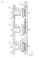
図2は本装置200の具体的な一部平面構成図を示す。
FIG. 2 shows a specific partial plan view of the
第1の画素電極間W1には、上記の通り、隣接する各画素電極1に接続された2つのTFT2がY方向に形成され、かつ2本のゲート配線5がX方向に互いに平行に形成されている。データ配線3は、上記の通りY方向に配線され、かつ2本のゲート配線5と交差するところで当該2本のゲート配線5の間のX方向に延出して配置されている。当該延出されたデータ配線(データ配線延出部)3aは、2つのTFT2のドレイン電極に共通接続されている。
As described above, in the first inter-pixel electrode W1, two
第2の画素電極間W2には、上記の通り、2本の補助容量配線6と、Y座標検知配線7と、が配置されている。
The second inter-pixel electrodes W2, as described above, the two
また、X座標検知配線4から延出されたX座標検知接点部9がY座標検知配線7に設けられている場合と、Y座標検知接点部10がY座標検知配線7に設けられている場合と、土台部11がY座標検知配線7に設けられている場合と、がある。
Further, the case where the X coordinate
この土台部11は、外部からの押圧を受けていないときのX座標検知接点部9及びY座標検知接点部10の各接点間隔を予め設定された接点間隔に設定する。
The
2本の補助容量配線6は隣接する各画素電極1と各補助容量8を形成し、互いに平行に設けられている。
The two
図3はX座標検知接点部9、Y座標検知接点部10及び土台部11に対応した、図2中のH−H部分に対応した断面図である。
FIG. 3 is a cross-sectional view corresponding to the HH portion in FIG. 2 corresponding to the X coordinate
第1の基板(TFT基板)にはTFT2が形成されている。後述するようにTFT2は、例えばアルミニウムまたはクロムまたはモリブデンからなるゲート膜と、例えばシリコン窒化膜からなるゲート絶縁膜100と、例えば真性アモルファスシリコンからなる真性シリコン膜と、例えばシリコン窒化膜からなるチャネル保護膜と、例えばn+アモルファスシリコンからなるn+シリコン膜と、例えばアルミニウムまたはクロムまたはモリブデンからなるソース・ドレイン膜と、例えばシリコン窒化膜からなるオーバーコート絶縁膜101と、を積層して形成されている。
A
X座標検知接点部9、Y座標検知接点部10及び土台部11には、後述するようにそれぞれTFT2の積層構造と同じ各積層構造102が形成されている。
Each of the X coordinate
一方、第2の基板(カラーフィルタ基板)には、カラーフィルタ103と、ブラックマトリックス104と、複数の接点用突起部105と、が設けられている。これら接点用突起105は、それぞれX座標検知接点部9、Y座標検知接点部10及び土台部11の各部分に対峙して設けられている。これら接点用突起部105、カラーフィルタ103及びブラックマトリックス104上には、対向電極20が設けられている。
On the other hand, the second substrate (color filter substrate), a
X座標検知接点部9は、オーバーコート絶縁膜101上に画素電極と同じ材料(例えばITO)を使用してX座標検知接点電極106が形成され、このX座標検知接点電極106が積層構造102中のX座標検知配線4に接続されている。これにより、X座標検知接点部9は、外部からの押圧を受けて対向電極(接点)20とX座標検知接点電極106とが導通すると、X座標検知配線4にX座標信号を生じせしめる。
In the X coordinate
Y座標検知接点部10は、オーバーコート絶縁膜101上に画素電極と同じ材料(例えばITO)を使用してY座標検知接点電極107が形成され、このY座標検知接点電極107が積層構造102中のY座標検知配線7に接続されている。これにより、Y座標検知接点部10は、外部からの押圧を受けて対向電極(接点)20とY座標検知接点電極107とが導通すると、Y座標検知配線7にY座標信号を生じせしめる。
In the Y coordinate
土台部11は、オーバーコート絶縁膜101上に画素電極と同じ材料(例えばITO)を使用して電極108が形成され、さらに例えばシリコン窒化膜からなる絶縁体の高さ調整部11aを形成して配置されている。そして、接点用突起部105が柱状スペーサの役割を果たして高さ調整部11aに接触している。これにより、外部からの押圧を受けていないときのX座標検知接点部9とY座標検知接点部10との各接点間隔、すなわちX座標検知接点部9であれば対向電極(接点)20とX座標検知接点電極106との接点間隔K1、Y座標検知接点部10であれば対向電極(接点)20とY座標検知接点電極107との接点間隔K2は、予め設定された同じ接点間隔に設定される。
The
次に、図4乃至図8を参照しながら、第1の基板上におけるTFT2、X座標検知接点部9、Y座標検知接点部10及び土台部11に共通の作成工程について詳しく説明する。
Next, with reference to FIG. 4 to FIG. 8, a production process common to the
なお、図4乃至図8(A)では、TFT2が順次形成される様子が、図2のIVA−IVA部分に対応した断面図において示されている。
4A to 8A, the state in which the
また、図4乃至図8(B)では、(A)のTFT2の作成と同時に土台部11が順次形成される様子が、図1のIVB−IVB部分に対応した断面図において示されている。
FIGS. 4 to 8B are cross-sectional views corresponding to the IVB-IVB portion of FIG. 1, showing that the
また、図4乃至図8(C)では、(A)のTFT2の作成と同時にX座標検知接点部9が順次形成される様子が、図1のIVC−IVC部分に対応した断面図において示されている。
4 to 8C, a state in which the X coordinate
また、図4乃至図8(D)では、(A)のTFT2の作成と同時にY座標検知接点部10が順次形成される様子が、図1のIVD−IVD部分に対応した断面図において示されている。
Further, in FIGS. 4 to 8D, a state in which the Y coordinate
最初は図4(A)〜(D)に図示されているように、第1基板上にフォトリソグラフィ法により、例えばアルミニウムまたはクロムまたはモリブデンからなるゲート膜を使用してゲート配線5及びゲート配線5に沿い延伸しているY座標検知配線7が形成される。そして、ゲート配線5においてTFT2に対応した部分はTFT2のためのゲート電極5cを提供している。またY座標検知配線7においてY座標検知接点部10に対応した部分はY座標検知用接点部10のための接続部分7bを提供している。
First, as shown in FIGS. 4A to 4D, the
次に、図5(A)〜(D)に図示されているように、第1基板上には例えばシリコン窒化膜(SiNx)を使用した透明なゲート絶縁膜100がゲート配線5及びY座標検知配線7を覆うように形成される。
Next, as illustrated in FIGS. 5A to 5D, a transparent
次に、例えば真性アモルファスシリコンからなるa−Si層52及び例えばn+アモルファスシリコンからなるn+a−Si層54が、部分的に例えばSiNxを使用したチャネル保護膜56を間に介して、積層される。
Next, an
次に、n+a−Si層54を覆うように例えばアルミニウムまたはクロムまたはモリブデンからなるソース・ドレイン膜58が形成される。ソース・ドレイン膜58は、TFT2の近傍のデータ配線3及びX座標検知接点部9の近傍のX座標検知配線4を提供している。
Next, a source /
そして、X座標検知配線4においてX座標検知接点部9に対応した部分は、X座標検知接点部9のための接続部分4bを提供している。
The portion corresponding to the X coordinate
n+a−Si層54及びソース・ドレイン膜58は、図4(A)中に示されているように、画素電極1に近い側と画素電極1から遠い側とで2分割される。
As shown in FIG. 4A, the n + a-Si layer 54 and the source /
a−Si層52、チャネル保護膜56,そしてこの様に2分割されたn+a−Si層54の積層の組み合わせは、TFT2のオーミックス層24dを提供している。また、このように2分割されたソース・ドレイン膜58は、画素電極1に近い側がTFT2のソース電極24aを、また画素電極1から遠い側がTFT2においてデータ配線3から延びているドレイン電極24bを提供している。
The laminated combination of the
次に、図6(A)〜(D)中に図示されているように、ソース・ドレイン膜58を覆う例えばシリコン窒化膜(SiNx)を使用した透明なオーバーコート絶縁膜101が形成される。
Next, as shown in FIGS. 6A to 6D, a transparent
ここで、図6(A)中に図示されているように、オーバーコート絶縁膜101においてTFT2の対応部分においては、ソース・ドレイン膜58のソース電極24aに対応した位置にソース電極24aを露出させるためのコンタクトホール101aが形成される。コンタクトホール101aは、図2中にも図示されている。
Here, as illustrated in FIG. 6A, the
また、図6(C)中に図示されているように、オーバーコート絶縁膜101においてX座標検知配線4のX座標検知接点部9のための接続部分4bに対応した部分に接続部分4bを露出させるためのコンタクトホール101bが形成される。コンタクトホール101bは、図2中にも図示されている。
Further, as shown in FIG. 6C, the
さらに、図6(D)中に図示されているように、オーバーコート絶縁膜101においてY座標検知配線7のY座標検知接点部10のための接続部分7bに対応した部分に接続部分7bを露出させるためのコンタクトホール101cが形成される。コンタクトホール101cは、オーバーコート絶縁膜101とY座標検知接点部10のための接続部分7bとの間に存在しているゲート絶縁膜100も貫通している。コンタクトホール101cは、図2中にも図示されている。
Further, as shown in FIG. 6D, the
この段階で、図6(A)中に図示されているTFT2の対応部分においては、ゲート配線5によるゲート電極5c、ゲート電極5cに重なったゲート絶縁膜100の部分、ゲート絶縁膜100の前記部分に重なった、a−Si層52、チャネル保護膜56、そして2分割されたn+a−Si膜54を含む半導体のためのオーミックス層24d、オーミックス層24dの2分割されたn+a−Si膜54上のソース電極24a及びドレイン電極24b、そしてソース電極24a及びドレイン電極24bを覆うオーバーコート絶縁膜101が、TFT2を提供している。
At this stage, in the corresponding portion of the
次に、図7(A)〜(D)中に図示されているように、オーバーコート絶縁膜101を覆うよう例えばITOからなる透明導電膜62が形成される。
Next, as illustrated in FIGS. 7A to 7D, a transparent
透明導電膜62は、図7(A)中に図示されているように、ソース電極24aを露出させるためのコンタクトホール101a中にも形成されてソース電極24aと電気的に接続される。透明導電膜62はまた、図7(C)中に図示されているように、X座標検知接点部9のための接続部分4bを露出させるためのコンタクトホール101b中にも形成されて接続部分4bと電気的に接続される。透明導電膜62はさらに、図7(D)中に図示されているように、Y座標検知接点部10のための接続部分7bを露出させるためのコンタクトホール101c中にも形成されて接続部分7bと電気的に接続される。
As shown in FIG. 7A, the transparent
透明導電膜62が形成された時点で、図7(A)〜(D)中に図示されているTFT2の断面の一部、土台部11の断面の一部、X座標検知接点部9の断面の一部、そしてY座標検知接点部10の断面の一部のそれぞれは、TFT2を形成するための前述した作成方法によって第1基板上に共通して同時に形成されているので、第1基板上からの高さは相互に同じである。
When the transparent
次に、土台部11の断面の一部を示している図7(B)においては、透明導電膜62の上にさらに、所定の高さの例えばシリコン窒化膜(SiNx)を使用した透明な土台部絶縁膜により高さ調整部11aが形成され、その頂点が土台部11の突出端面(先端)311bを提供している。
Next, in FIG. 7B showing a part of the cross section of the
最後に透明導電膜62は、TFT2の対応部分では図7(A)に中に示されているように、ソース電極24aと電気的に接続されたコンタクトホール101a中の部分及びTFT2に隣接した画素電極1を提供する部分を除き削除される。
Finally, as shown in FIG. 7A, the transparent
また最後に透明導電膜62は、土台部11の対応部分では図7(B)に中に示されているように、高さ調整部11aに覆われている部分108を除き削除される。
Finally, the transparent
また最後に透明導電膜62は、X座標検知接点部9の対応部分及びX座標検知配線4の接続部分4bでは図7(C)中に示されているように、X座標検知接点電極106を提供するX座標検知接点部9の対応部分及びX座標検知接点部9をX座標検知配線4の接続部分4bに電気的に接続させるコンタクトホール101b中の部分を除き削除される。
Finally, as shown in FIG. 7C, the transparent
さらに最後に透明導電膜62は、Y座標検知接点部10の対応部分及びY座標検知配線7の接続部分7bでは図7(D)中に示されているように、Y座標検知接点電極107を提供するY座標検知接点部10の対応部分及びY座標検知接点部10をY座標検知配線7の接続部分7bに電気的に接続させるコンタクトホール101c中の部分を除き除去される。
Finally, the transparent
図7(A)〜(D)を見比べると、以下のことがわかる。即ち、第1基板から図7(C)に示されているX座標検知接点部9の突出端面(先端)までの高さ及び図7(D)に示されているY座標検知接点部10の突出端面(先端)までの高さは相互に同じである。
Comparison of FIGS. 7A to 7D reveals the following. That is, the height from the first substrate to the protruding end surface (tip) of the X coordinate
第1基板から図7(A)に示されているTFT2の突出端面(先端)までの高さは、図7(C)に示されている前述したX座標検知接点部9の突出端面(先端)までの高さ及び図7(D)に示されているY座標検知接点部10の突出端面(先端)までの高さよりも、最後にTFT2の突出端面(先端)から除去された透明導電膜62の厚さ分だけ低い。
The height from the first substrate to the protruding end face (tip) of the
さらに、第1基板から土台部11の突出端面(先端)11bまでの高さは、図7(C)に示されている前述したX座標検知接点部9の突出端面(先端)までの高さ及び図7の(D)に示されているY座標検知接点部10の突出端面(先端)までの高さよりも、最後に透明導電膜62の上に形成された高さ調整部11aの突出端面(先端)11bまでの高さ分だけ高い。
Further, the height from the first substrate to the protruding end surface (tip) 11b of the
これに対して図9は従来のタッチパネルの具体的な一部拡大した平面構成図を示す。Y方向の各画素電極1の間Mにはそれぞれ、TFT2が配置されると共に、ゲート配線5と、補助容量配線6と、Y座標検知配線7と、が配置されている。
On the other hand, FIG. 9 shows a specific partially enlarged plan view of a conventional touch panel. A
また、X座標検知配線4から延出されたX座標検知接点部9がY座標検知配線7に設けられている場合と、Y座標検知接点部10がY座標検知配線7に設けられている場合と、土台部11がY座標検知配線7に設けられている場合と、がある。
Further, the case where the X coordinate
本装置200と従来装置とを比較すると、本装置200の第1の画素電極間W1のY方向の間隔Laは、従来装置の電極間Mの間隔Lmよりも狭く形成されている(La<Lm)。本装置200の第2の画素電極間W2のY方向の間隔Lbも、従来装置の電極間Mの間隔Lmよりも狭く形成されている(Lb<Lm)。
Comparing the
従って、本装置200の各画素電極1のY方向の長さは、従来装置の各画素電極1のY方向の長さよりも長く形成することができる。これにより、本装置200の各画素電極1の面積Saは、従来装置の各画素電極1の面積Sbよりも広くすることが出来る。
Accordingly, the length in the Y direction of each
図10は本装置200の各画素電極1の面積Saと従来装置の各画素電極1の面積Sbとの対比結果を示す。本装置200の各画素電極1のX方向の長さは、従来装置の各画素電極1の同方向の長さと同一であるものの、各画素電極1のY方向の長さは、本装置200の方が従来装置よりも長くなっている。これにより、本装置200の各画素電極1の面積Saは、従来装置の各画素電極1の面積Sbよりも広くなっている。
FIG. 10 shows a comparison result between the area Sa of each
図10から、本装置200と従来装置とを比較すると、本装置200のY座標検知配線7の総本数とX座標検知接点部9とY座標検知接点部10と土台部11の総数は従来装置の半分である。
From FIG. 10, when comparing the
例えば、奇数行の画素は従来装置のレイアウトのままであり、偶数行の画素は従来装置のレイアウトからY座標検知配線7とX座標検知接点部9とY座標検知接点部10と土台部11を取り去って、その分偶数行の画素の開口率を向上させることは可能であるが、奇数行の画素よりも偶数行の画素の方が大きい開口率になってしまうために全白表示をおこなうと1行置きの横縞表示となってしまう。結局、全白表示の均一性を得るためには偶数行で向上した開口率分をブラックマスクで覆って従来の開口率に合わせることになり、このようなやり方では開口率は向上しない。
For example, the odd-numbered pixels remain in the layout of the conventional device, and the even-numbered pixels have the Y coordinate
本装置200のY座標検知配線7の総本数が従来装置の半分であることは、本装置200のY座標検知精度が従来装置の半分であることを意味する。しかしながら、携帯電話やデジタルカメラで代表的な対角2.5インチQVGA(240×320画素)及び電子辞書や産業機器等で代表的な対角5.0インチVGA(480×640画素)の画素ピッチは0.159mmであり、2倍にしても0.318mmである。これに対してタッチするのに使うペン先の代表的な直径は0.5mm程度であり、指先でタッチする場合はペン先よりもはるかに直径が大きいことを考えると、本装置200のY座標検知精度が従来装置の半分であることはタッチパネルの検出精度として問題ない。
That the total number of Y coordinate
このように上記一実施の形態によれば、第1の画素電極間W1に2つのTFT2と2本のゲート配線5とを形成し、かつ第2の画素電極間W2に2本の補助容量配線6とY座標検知配線7とを設け、さらにX座標検知接点部9またはY座標検知接点部10または土台部11、をY座標検知配線7に設ける配線レイアウトにしたので、第1の画素電極間W1の間隔Laと第2の画素電極間W2の間隔Lbとを従来装置の画素電極間の間隔よりも狭くすることができ、この結果として本装置200としての開口率を大きくすることができ、本装置200の表示性能、例えば表示の輝度等の画質を向上することが出来る。
As described above, according to the embodiment, two
また、第1の画素電極間W1内において、データ配線3を2本のゲート配線5と交差するところで当該2本のゲート配線5の間に延出して配置し、当該延出されたデータ配線延出部3aを2つのTFT2のドレイン電極に共通接続した配線レイアウトにしたので、データ配線3を2本のゲート配線5と交差するところで当該2本のゲート配線5の間に2つ延出して配置し、当該延出された一方のデータ配線延出部を一方のTFT2のドレイン電極に接続し、当該延出された他方のデータ配線延出部を他方のTFT2のドレイン電極接続した配線レイアウトと比較して、第1の画素電極間W1のY方向における長さを短くでき、開口率を向上できる。
Further, in the first inter-pixel electrode W1, the data wiring 3 is arranged so as to extend between the two
なお、本発明は上記実施形態そのままに限定されるものではなく、実施段階ではその要旨を逸脱しない範囲で構成要素を変形して具体化できる。また、上記実施形態に開示されている複数の構成要素の適宜な組み合わせにより、種々の発明を形成できる。例えば、実施形態に示される全構成要素から幾つかの構成要素を削除してもよい。さらに、異なる実施形態にわたる構成要素を適宜組み合わせてもよい。 Note that the present invention is not limited to the above-described embodiment as it is, and can be embodied by modifying the constituent elements without departing from the scope of the invention in the implementation stage. In addition, various inventions can be formed by appropriately combining a plurality of components disclosed in the embodiment. For example, some components may be deleted from all the components shown in the embodiment. Furthermore, constituent elements over different embodiments may be appropriately combined.
1:画素電極、2:薄膜トランジスタ(TFT)、3:データ配線(信号線)、4:X座標検知配線、5:ゲート配線(走査線)、6:補助容量配線、7:Y座標検知配線、8:補助容量、9:X座標検知接点部、10:Y座標検知接点部、11:土台部、200:本装置、20:対向電極、W1:第1の画素電極間隔、W2:第2の画素電極間隔、21:データドライバ(データ駆動回路)、22:走査ドライバ(走査駆動回路)、23:X座標検出部、25:Y座標検出部、Q:液晶層。 1: pixel electrode, 2: thin film transistor (TFT), 3: data wiring (signal line), 4: X coordinate detection wiring, 5: gate wiring (scanning line), 6: auxiliary capacitance wiring, 7: Y coordinate detection wiring, 8: Auxiliary capacitance, 9: X coordinate detection contact part, 10: Y coordinate detection contact part, 11: Base part, 200: This device, 20: Counter electrode, W1: First pixel electrode interval, W2: Second Pixel electrode spacing, 21: data driver (data drive circuit), 22: scan driver (scan drive circuit), 23: X coordinate detection unit, 25: Y coordinate detection unit, Q: liquid crystal layer.
Claims (8)
前記第1の基板と前記第2の基板との間に封入された液晶層と、
前記第1の基板に設けられ、第1の方向と、当該第1の方向と垂直な第2の方向と、に配列された複数の画素電極と、
前記第2の基板に設けられ、前記複数の画素電極に対して対向配置される対向電極と、
前記複数の画素電極にそれぞれ接続された複数の画素用トランジスタと、
前記複数の画素用トランジスタに走査信号を供給する前記第1の方向に延伸する複数の走査線と、
前記複数の画素用トランジスタに表示信号を供給する前記第2の方向に延伸する複数の信号線と、
前記複数の画素電極との間に補助容量を形成する前記第1の方向に延伸する複数の補助容量線と、
前記第1の方向に延伸された複数の第1の座標検知配線と、
前記第2の方向に延伸された複数の第2の座標検知配線と、
前記第2の基板にそれぞれ設けられ、前記対向電極を接点電極とする複数の第1の接点突起部及び複数の第2の接点突起部と、
前記第2の基板に設けられた複数の柱状スペーサと、
前記複数の第1の座標検知配線にそれぞれ接続されており、前記第2基板が外部からの押圧を受けたときに前記複数の第1の接点突起部と導通する複数の第1の座標検知接点部と、
前記複数の第2の座標検知配線にそれぞれ接続されており、前記第2基板が外部からの押圧を受けたときに前記複数の第2の接点突起部と導通する複数の第2の座標検知接点部と、
前記第2基板が外部からの押圧を受けていないときに、前記複数の第1の接点突起部のそれぞれと前記複数の第1の接点突起部のそれぞれに対応する前記複数の第1の座標検知接点部のそれぞれとの間隔、及び、前記複数の第2の接点突起部のそれぞれと前記複数の第2の接点突起部のそれぞれに対応する前記複数の第2の座標検知接点部のそれぞれとの間隔をそれぞれ保持するために前記複数の柱状スペーサが接触する、複数の土台部と、
を備え、
前記第2の方向に隣接する前記複数の画素電極の複数の間隔のうちの、
複数の第1の画素電極間隔には、前記第2の方向に隣接する各画素電極に接続された前記各画素用トランジスタと、前記各画素用トランジスタに接続された前記各走査線と、前記信号線から延出された信号線延出部と、が配置されるとともに、前記各補助容量線と、前記第1の座標検出検知線と、は配置されず、
複数の第2の画素電極間隔には、前記第2の方向に隣接する各画素電極に対応した前記各補助容量線と、前記第1の座標検出検知線と、が配置されるとともに、前記各画素用トランジスタと、前記各走査線と、前記信号線延出部と、は配置されず、
前記複数の第2の画素電極間隔における前記第1の座標検出検知線上には、前記複数の第1の座標検知接点部、前記複数の第2の座標検知接点部及び前記複数の土台部が形成されている、
ことを特徴とするタッチパネル。 A first substrate and a second substrate disposed opposite to each other;
A liquid crystal layer sealed between the first substrate and the second substrate;
A plurality of pixel electrodes provided on the first substrate and arranged in a first direction and a second direction perpendicular to the first direction;
A counter electrode provided on the second substrate and disposed to face the plurality of pixel electrodes;
A plurality of pixel transistors respectively connected to the plurality of pixel electrodes;
A plurality of scanning lines extending in the first direction for supplying a scanning signal to the plurality of pixel transistors;
A plurality of signal lines extending in the second direction for supplying a display signal to the plurality of pixel transistors;
A plurality of storage capacitor lines extending in the first direction to form storage capacitors between the plurality of pixel electrodes;
A plurality of first coordinate detection wires extending in the first direction;
A plurality of second coordinate detection wires extended in the second direction;
A plurality of first contact protrusions and a plurality of second contact protrusions, each provided on the second substrate and having the counter electrode as a contact electrode;
A plurality of columnar spacers provided on the second substrate;
A plurality of first coordinate detection contacts that are respectively connected to the plurality of first coordinate detection wirings and that are electrically connected to the plurality of first contact protrusions when the second substrate receives an external pressure. And
A plurality of second coordinate detection contacts that are respectively connected to the plurality of second coordinate detection wirings and that are electrically connected to the plurality of second contact protrusions when the second substrate is pressed from outside. And
The plurality of first coordinate detections corresponding to each of the plurality of first contact protrusions and each of the plurality of first contact protrusions when the second substrate is not subjected to external pressure. A distance from each of the contact portions, and each of the plurality of second contact protrusions and each of the plurality of second coordinate detection contact portions corresponding to each of the plurality of second contact protrusions. A plurality of base portions that are in contact with the plurality of columnar spacers in order to maintain the spacing;
Equipped with a,
Of a plurality of intervals between the plurality of pixel electrodes adjacent in the second direction,
The plurality of first pixel electrode intervals include the pixel transistors connected to the pixel electrodes adjacent in the second direction, the scan lines connected to the pixel transistors, and the signal. Rutotomoni a signal line extending portion extending from the line, is arranged, wherein each auxiliary capacitance line, wherein the first coordinate detection detection line, are not disposed,
The auxiliary capacitor lines corresponding to the pixel electrodes adjacent in the second direction and the first coordinate detection detection lines are arranged in the plurality of second pixel electrode intervals, The pixel transistor, each scanning line, and the signal line extending portion are not arranged,
The plurality of first coordinate detection contact portions, the plurality of second coordinate detection contact portions, and the plurality of base portions are formed on the first coordinate detection detection lines in the plurality of second pixel electrode intervals. Being
A touch panel characterized by that.
前記第2の方向に隣接する一方の前記画素電極に接続された一方の前記画素用トランジスタと、当該一方の画素用トランジスタに接続された一方の前記走査線と、が配置され、
前記第2の方向に隣接する他方の前記画素電極に接続された他方の前記画素用トランジスタと、当該他方の画素用トランジスタに接続された他方の前記走査線と、が配置され、
前記一方の走査線と前記他方の走査線との間に前記信号線延出部が配置され、前記信号線延出部が前記一方の画素用トランジスタと前記他方の画素用トランジスタとに共通接続されることで、前記一方の画素用トランジスタと前記他方の画素用トランジスタとが前記第2の方向に隣接する、
ことを特徴とする請求項1に記載のタッチパネル。 In the plurality of first pixel electrode intervals,
One pixel transistor connected to one pixel electrode adjacent in the second direction and one scanning line connected to the one pixel transistor are disposed,
The other pixel transistor connected to the other pixel electrode adjacent in the second direction and the other scanning line connected to the other pixel transistor are disposed,
The signal line extending portion is disposed between the one scanning line and the other scanning line, and the signal line extending portion is commonly connected to the one pixel transistor and the other pixel transistor. Thus, the one pixel transistor and the other pixel transistor are adjacent to each other in the second direction.
The touch panel according to claim 1.
前記第2の方向に隣接する一方の前記画素電極に対応する一方の前記補助容量線と、前記第2の方向に隣接する他方の前記画素電極に対応する他方の前記補助容量線と、が配置され、
前記一方の補助容量線と前記他方の補助容量線との間に前記第1の座標検出検知線が配置される、
ことを特徴とする請求項1又は2に記載のタッチパネル。 In the plurality of second pixel electrode intervals,
The one wherein the storage capacitance line corresponding to a second one of the pixel electrodes of the adjacent direction of the other of the storage capacitor line corresponding to the pixel electrode of the other adjacent to the second direction, is arranged And
The first coordinate detection detection line is disposed between the one auxiliary capacitance line and the other auxiliary capacitance line;
The touch panel according to claim 1 or 2 .
ことを特徴とする請求項1乃至3のいずれか1項に記載のタッチパネル。 The first pixel electrode interval and the second pixel electrode interval are alternately arranged along the second direction.
The touch panel according to any one of claims 1 to 3, wherein the touch panel is provided.
前記第2の座標検知配線は、前記第3の画素電極列と前記第4の画素電極列との間に配設され、
前記複数の信号線は、第1の信号線、第2の信号線、第3の信号線、第4の信号線を含み、
第1の信号線は、前記第1の画素電極列と前記第2の画素電極列との間に配設され、
第2の信号線は、前記第2の画素電極列と前記第3の画素電極列との間に配設され、
第3の信号線は、前記第2の座標検知配線と前記第4の画素電極列との間に配設され、
第4の信号線は、前記第4の画素電極列と前記第5の画素電極列との間に配設され、
前記複数の第2の画素電極間隔における前記第1の座標検出検知線上には、
前記土台部が前記第1の信号線と前記第2の信号線との間に配置され、
前記第2の座標検知接点部が前記第2の信号線と前記第3の信号線との間に配置され、
前記第1の座標検知接点部が前記第3の信号線と前記第4の信号線との間に配置されている、
ことを特徴とする請求項1乃至4のいずれか1項に記載のタッチパネル。 The plurality of pixel electrodes include a first pixel electrode column, a second pixel electrode column, a third pixel electrode column, a fourth pixel electrode column, and a fifth pixel array that are continuously arranged in the first direction. Including pixel electrode rows,
The second coordinate detection wiring is disposed between the third pixel electrode row and the fourth pixel electrode row,
The plurality of signal lines include a first signal line, a second signal line, a third signal line, and a fourth signal line,
The first signal line is disposed between the first pixel electrode column and the second pixel electrode column,
The second signal line is disposed between the second pixel electrode column and the third pixel electrode column,
The third signal line is disposed between the second coordinate detection wiring and the fourth pixel electrode column,
The fourth signal line is disposed between the fourth pixel electrode column and the fifth pixel electrode column,
On the first coordinate detection detection line in the plurality of second pixel electrode intervals,
The base is disposed between the first signal line and the second signal line;
The second coordinate detection contact portion is disposed between the second signal line and the third signal line;
The first coordinate detection contact portion is disposed between the third signal line and the fourth signal line;
The touch panel according to any one of claims 1 to 4 , wherein the touch panel is provided.
前記複数の第1の座標検知接点部及び前記複数の第2の座標検知接点部は、それぞれ同じ高さに形成され、
前記複数の土台部は、前記複数の第1の座標検知接点部及び前記複数の第2の座標検知接点部よりもそれぞれ高く形成されている、
ことを特徴とする請求項1乃至5のいずれか1項に記載のタッチパネル。 The plurality of first contact protrusions, the plurality of second contact protrusions, and the plurality of columnar spacers are each formed of the same material and are formed at the same height,
The plurality of first coordinate detection contact portions and the plurality of second coordinate detection contact portions are respectively formed at the same height,
The plurality of base portions are formed higher than the plurality of first coordinate detection contact portions and the plurality of second coordinate detection contact portions, respectively.
The touch panel according to claim 1 , wherein the touch panel is provided.
ことを特徴とする請求項1乃至6のいずれか1項に記載のタッチパネル。 The first coordinate detection contact portion and the second coordinate detection contact portion are formed using at least a part of a plurality of materials of the pixel transistor.
The touch panel according to any one of claims 1 to 6, characterized in that.
ことを特徴とする請求項1乃至7のいずれか1項に記載のタッチパネル。 The base portion includes a base portion formed by using at least a part of a plurality of materials of the pixel transistor, and a height adjustment portion formed after the pixel transistor is formed, and is formed by laminating. Being
The touch panel according to any one of claims 1 to 7, characterized in that.
Priority Applications (1)
| Application Number | Priority Date | Filing Date | Title |
|---|---|---|---|
| JP2010212640A JP5573540B2 (en) | 2010-09-22 | 2010-09-22 | Touch panel |
Applications Claiming Priority (1)
| Application Number | Priority Date | Filing Date | Title |
|---|---|---|---|
| JP2010212640A JP5573540B2 (en) | 2010-09-22 | 2010-09-22 | Touch panel |
Publications (3)
| Publication Number | Publication Date |
|---|---|
| JP2012068405A JP2012068405A (en) | 2012-04-05 |
| JP2012068405A5 JP2012068405A5 (en) | 2013-10-31 |
| JP5573540B2 true JP5573540B2 (en) | 2014-08-20 |
Family
ID=46165772
Family Applications (1)
| Application Number | Title | Priority Date | Filing Date |
|---|---|---|---|
| JP2010212640A Expired - Fee Related JP5573540B2 (en) | 2010-09-22 | 2010-09-22 | Touch panel |
Country Status (1)
| Country | Link |
|---|---|
| JP (1) | JP5573540B2 (en) |
Families Citing this family (4)
| Publication number | Priority date | Publication date | Assignee | Title |
|---|---|---|---|---|
| US10809581B2 (en) | 2014-11-21 | 2020-10-20 | Sharp Kabushiki Kaisha | Active matrix substrate, and display panel |
| TWI657301B (en) * | 2014-11-21 | 2019-04-21 | 日商夏普股份有限公司 | Active-matrix substrate and display panel |
| KR102509610B1 (en) * | 2017-11-08 | 2023-03-14 | 삼성디스플레이 주식회사 | Fingerprint sensor and display device including the same |
| CN116700519B (en) * | 2021-11-30 | 2024-04-12 | 荣耀终端有限公司 | Touch display panel, driving method and touch display device |
Family Cites Families (6)
| Publication number | Priority date | Publication date | Assignee | Title |
|---|---|---|---|---|
| JPS6473324A (en) * | 1987-09-14 | 1989-03-17 | Matsushita Electric Ind Co Ltd | Display device and its driving method |
| JP2714993B2 (en) * | 1989-12-15 | 1998-02-16 | セイコーエプソン株式会社 | Liquid crystal display |
| JP2000099268A (en) * | 1998-09-21 | 2000-04-07 | Nec Eng Ltd | Liquid crystal display device with coordinate position detecting function |
| KR101297387B1 (en) * | 2006-11-09 | 2013-08-19 | 삼성디스플레이 주식회사 | Liquid crystal display associated with touch panel |
| KR101349096B1 (en) * | 2006-12-27 | 2014-01-09 | 삼성디스플레이 주식회사 | Display device |
| EP2333604A4 (en) * | 2008-09-30 | 2012-04-18 | Sharp Kk | Display device |
-
2010
- 2010-09-22 JP JP2010212640A patent/JP5573540B2/en not_active Expired - Fee Related
Also Published As
| Publication number | Publication date |
|---|---|
| JP2012068405A (en) | 2012-04-05 |
Similar Documents
| Publication | Publication Date | Title |
|---|---|---|
| US10042490B2 (en) | Array substrate, display device and driving method | |
| JP5229312B2 (en) | Liquid crystal display | |
| US9292139B2 (en) | Capacitive in-cell touch screen panel and display device | |
| US9423916B2 (en) | In-cell touch panel and display device | |
| JP4811502B2 (en) | Liquid crystal display panel and touch panel | |
| WO2019196632A1 (en) | Array substrate and preparation method therefor, and display panel and display device | |
| JP4900421B2 (en) | Liquid crystal display panel and liquid crystal display device | |
| US9213441B2 (en) | In-cell touch panel and liquid crystal device | |
| US11016591B2 (en) | Touch-sensitive display device and display panel | |
| US20210151513A1 (en) | Display device | |
| JP5056702B2 (en) | Liquid crystal display element and liquid crystal display device | |
| JP5573540B2 (en) | Touch panel | |
| US20240061521A1 (en) | Array substrate and touch display device | |
| TWI439778B (en) | Pixel array substrate and display panel | |
| US20120013593A1 (en) | Display device | |
| JP6652901B2 (en) | Display device and method of manufacturing the same | |
| JP2012068405A5 (en) | ||
| KR102352750B1 (en) | Touch Display Device | |
| JP6564896B2 (en) | Display device | |
| JP6800355B2 (en) | Display device and its manufacturing method | |
| US20240069666A1 (en) | Mini led touch panel and its driving method and preparation method | |
| JP2020140489A (en) | In-cell touch panel | |
| CN111505874A (en) | Display device | |
| JP2012128070A (en) | Electronic device | |
| JP2020140075A (en) | In-cell touch panel |
Legal Events
| Date | Code | Title | Description |
|---|---|---|---|
| A521 | Written amendment |
Free format text: JAPANESE INTERMEDIATE CODE: A523 Effective date: 20130912 |
|
| A621 | Written request for application examination |
Free format text: JAPANESE INTERMEDIATE CODE: A621 Effective date: 20130912 |
|
| A977 | Report on retrieval |
Free format text: JAPANESE INTERMEDIATE CODE: A971007 Effective date: 20140221 |
|
| A131 | Notification of reasons for refusal |
Free format text: JAPANESE INTERMEDIATE CODE: A131 Effective date: 20140225 |
|
| A521 | Written amendment |
Free format text: JAPANESE INTERMEDIATE CODE: A523 Effective date: 20140428 |
|
| TRDD | Decision of grant or rejection written | ||
| A01 | Written decision to grant a patent or to grant a registration (utility model) |
Free format text: JAPANESE INTERMEDIATE CODE: A01 Effective date: 20140603 |
|
| A61 | First payment of annual fees (during grant procedure) |
Free format text: JAPANESE INTERMEDIATE CODE: A61 Effective date: 20140616 |
|
| R150 | Certificate of patent or registration of utility model |
Ref document number: 5573540 Country of ref document: JP Free format text: JAPANESE INTERMEDIATE CODE: R150 |
|
| S111 | Request for change of ownership or part of ownership |
Free format text: JAPANESE INTERMEDIATE CODE: R313113 |
|
| R350 | Written notification of registration of transfer |
Free format text: JAPANESE INTERMEDIATE CODE: R350 |
|
| R250 | Receipt of annual fees |
Free format text: JAPANESE INTERMEDIATE CODE: R250 |
|
| R250 | Receipt of annual fees |
Free format text: JAPANESE INTERMEDIATE CODE: R250 |
|
| R250 | Receipt of annual fees |
Free format text: JAPANESE INTERMEDIATE CODE: R250 |
|
| LAPS | Cancellation because of no payment of annual fees |