JP5229312B2 - Liquid crystal display - Google Patents

Liquid crystal display Download PDF

Info

Publication number
JP5229312B2
JP5229312B2 JP2010288851A JP2010288851A JP5229312B2 JP 5229312 B2 JP5229312 B2 JP 5229312B2 JP 2010288851 A JP2010288851 A JP 2010288851A JP 2010288851 A JP2010288851 A JP 2010288851A JP 5229312 B2 JP5229312 B2 JP 5229312B2
Authority
JP
Japan
Prior art keywords
coordinate detection
pixel electrode
pixel
electrode
wiring
Prior art date
Legal status (The legal status is an assumption and is not a legal conclusion. Google has not performed a legal analysis and makes no representation as to the accuracy of the status listed.)
Expired - Fee Related
Application number
JP2010288851A
Other languages
Japanese (ja)
Other versions
JP2012137562A (en
JP2012137562A5 (en
Inventor
和広 佐々木
Current Assignee (The listed assignees may be inaccurate. Google has not performed a legal analysis and makes no representation or warranty as to the accuracy of the list.)
Casio Computer Co Ltd
Original Assignee
Casio Computer Co Ltd
Priority date (The priority date is an assumption and is not a legal conclusion. Google has not performed a legal analysis and makes no representation as to the accuracy of the date listed.)
Filing date
Publication date
Application filed by Casio Computer Co Ltd filed Critical Casio Computer Co Ltd
Priority to JP2010288851A priority Critical patent/JP5229312B2/en
Priority to US13/335,136 priority patent/US20120162109A1/en
Priority to KR1020110139832A priority patent/KR101389198B1/en
Priority to TW100148185A priority patent/TWI471640B/en
Priority to CN201110436903.0A priority patent/CN102566819B/en
Publication of JP2012137562A publication Critical patent/JP2012137562A/en
Publication of JP2012137562A5 publication Critical patent/JP2012137562A5/ja
Application granted granted Critical
Publication of JP5229312B2 publication Critical patent/JP5229312B2/en
Expired - Fee Related legal-status Critical Current
Anticipated expiration legal-status Critical

Links

Images

Classifications

    • GPHYSICS
    • G06COMPUTING; CALCULATING OR COUNTING
    • G06FELECTRIC DIGITAL DATA PROCESSING
    • G06F3/00Input arrangements for transferring data to be processed into a form capable of being handled by the computer; Output arrangements for transferring data from processing unit to output unit, e.g. interface arrangements
    • G06F3/01Input arrangements or combined input and output arrangements for interaction between user and computer
    • G06F3/03Arrangements for converting the position or the displacement of a member into a coded form
    • G06F3/041Digitisers, e.g. for touch screens or touch pads, characterised by the transducing means
    • G06F3/0412Digitisers structurally integrated in a display
    • GPHYSICS
    • G02OPTICS
    • G02FOPTICAL DEVICES OR ARRANGEMENTS FOR THE CONTROL OF LIGHT BY MODIFICATION OF THE OPTICAL PROPERTIES OF THE MEDIA OF THE ELEMENTS INVOLVED THEREIN; NON-LINEAR OPTICS; FREQUENCY-CHANGING OF LIGHT; OPTICAL LOGIC ELEMENTS; OPTICAL ANALOGUE/DIGITAL CONVERTERS
    • G02F1/00Devices or arrangements for the control of the intensity, colour, phase, polarisation or direction of light arriving from an independent light source, e.g. switching, gating or modulating; Non-linear optics
    • G02F1/01Devices or arrangements for the control of the intensity, colour, phase, polarisation or direction of light arriving from an independent light source, e.g. switching, gating or modulating; Non-linear optics for the control of the intensity, phase, polarisation or colour 
    • G02F1/13Devices or arrangements for the control of the intensity, colour, phase, polarisation or direction of light arriving from an independent light source, e.g. switching, gating or modulating; Non-linear optics for the control of the intensity, phase, polarisation or colour  based on liquid crystals, e.g. single liquid crystal display cells
    • G02F1/133Constructional arrangements; Operation of liquid crystal cells; Circuit arrangements
    • GPHYSICS
    • G06COMPUTING; CALCULATING OR COUNTING
    • G06FELECTRIC DIGITAL DATA PROCESSING
    • G06F3/00Input arrangements for transferring data to be processed into a form capable of being handled by the computer; Output arrangements for transferring data from processing unit to output unit, e.g. interface arrangements
    • G06F3/01Input arrangements or combined input and output arrangements for interaction between user and computer
    • G06F3/03Arrangements for converting the position or the displacement of a member into a coded form
    • G06F3/041Digitisers, e.g. for touch screens or touch pads, characterised by the transducing means
    • G06F3/047Digitisers, e.g. for touch screens or touch pads, characterised by the transducing means using sets of wires, e.g. crossed wires
    • GPHYSICS
    • G09EDUCATION; CRYPTOGRAPHY; DISPLAY; ADVERTISING; SEALS
    • G09GARRANGEMENTS OR CIRCUITS FOR CONTROL OF INDICATING DEVICES USING STATIC MEANS TO PRESENT VARIABLE INFORMATION
    • G09G3/00Control arrangements or circuits, of interest only in connection with visual indicators other than cathode-ray tubes
    • G09G3/20Control arrangements or circuits, of interest only in connection with visual indicators other than cathode-ray tubes for presentation of an assembly of a number of characters, e.g. a page, by composing the assembly by combination of individual elements arranged in a matrix no fixed position being assigned to or needed to be assigned to the individual characters or partial characters
    • G09G3/34Control arrangements or circuits, of interest only in connection with visual indicators other than cathode-ray tubes for presentation of an assembly of a number of characters, e.g. a page, by composing the assembly by combination of individual elements arranged in a matrix no fixed position being assigned to or needed to be assigned to the individual characters or partial characters by control of light from an independent source
    • G09G3/36Control arrangements or circuits, of interest only in connection with visual indicators other than cathode-ray tubes for presentation of an assembly of a number of characters, e.g. a page, by composing the assembly by combination of individual elements arranged in a matrix no fixed position being assigned to or needed to be assigned to the individual characters or partial characters by control of light from an independent source using liquid crystals
    • GPHYSICS
    • G06COMPUTING; CALCULATING OR COUNTING
    • G06FELECTRIC DIGITAL DATA PROCESSING
    • G06F2203/00Indexing scheme relating to G06F3/00 - G06F3/048
    • G06F2203/041Indexing scheme relating to G06F3/041 - G06F3/045
    • G06F2203/04103Manufacturing, i.e. details related to manufacturing processes specially suited for touch sensitive devices

Landscapes

  • Engineering & Computer Science (AREA)
  • Theoretical Computer Science (AREA)
  • General Engineering & Computer Science (AREA)
  • Physics & Mathematics (AREA)
  • General Physics & Mathematics (AREA)
  • Human Computer Interaction (AREA)
  • Chemical & Material Sciences (AREA)
  • Crystallography & Structural Chemistry (AREA)
  • Nonlinear Science (AREA)
  • Liquid Crystal (AREA)
  • Computer Hardware Design (AREA)
  • Mathematical Physics (AREA)
  • Optics & Photonics (AREA)
  • Position Input By Displaying (AREA)
  • Devices For Indicating Variable Information By Combining Individual Elements (AREA)

Abstract

A display apparatus includes first and second coordinate detecting lines. Each second coordinate detecting line is arranged between a second and third of four pixel electrodes arranged in a first direction. Two signal lines are arranged between first and second pixel electrodes or between a third and fourth pixel electrodes. Pixel transistors are connected to the second and third pixel electrodes, facing each other across one second coordinate detecting line, and arranged far from the second coordinate detecting line. A first and a second coordinate detecting part are arranged between pixel transistors connected to the second and third pixel electrodes.

Description

本発明は、タッチパネル機能を有する液晶表示装置に関する。   The present invention relates to a liquid crystal display device having a touch panel function.

液晶表示装置には、タッチパネル機能を内蔵するものがある。この装置には、第1の基板(TFT基板)と第2の基板(カラーフィルタ基板)とが対向配置されている。TFT基板上には、複数の画素電極が第1の方向(X方向)と第2の方向(Y方向)とに一定間隔で形成されている。これら画素電極は、矩形状に形成されている。カラーフィルタ基板には、対向電極が形成されている。複数の画素電極と対向電極との間には、液晶が封入されて液晶層を形成している。   Some liquid crystal display devices have a built-in touch panel function. In this apparatus, a first substrate (TFT substrate) and a second substrate (color filter substrate) are arranged to face each other. On the TFT substrate, a plurality of pixel electrodes are formed at regular intervals in a first direction (X direction) and a second direction (Y direction). These pixel electrodes are formed in a rectangular shape. A counter electrode is formed on the color filter substrate. Liquid crystal is sealed between the plurality of pixel electrodes and the counter electrode to form a liquid crystal layer.

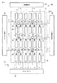
図15は同装置の平面配置図を示す。複数の画素電極1がX方向とY方向にそれぞれ一定間隔で配置されている。画素電極1の端部には、画素用トランジスタとしての薄膜トランジスタ(以下、TFTと称する)2が接続されている。各画素電極1のX方向における隣り合う間には、信号線としてのデータ配線3が配置されている。又、各画素電極1のX方向における隣り合う3つの間のうちの1つの間には、X座標検知配線4が配置されている。図15に示したように、各画素電極1のX方向における間には、図面上の左側から右側方向に順次、1本のデータ配線3、その右隣の間に1本のデータ配線3、さらにその右隣の間に1本のX座標検知配線4及び1本のデータ配線3、の順序で繰り返し配置されている。   FIG. 15 shows a plan layout of the apparatus. A plurality of pixel electrodes 1 are arranged at regular intervals in the X direction and the Y direction, respectively. A thin film transistor (hereinafter referred to as TFT) 2 as a pixel transistor is connected to the end of the pixel electrode 1. Between the pixel electrodes 1 adjacent to each other in the X direction, data wirings 3 as signal lines are arranged. Further, an X coordinate detection wiring 4 is arranged between one of three adjacent ones in the X direction of each pixel electrode 1. As shown in FIG. 15, between the pixel electrodes 1 in the X direction, one data line 3 is sequentially arranged from the left side to the right side in the drawing, and one data line 3 is adjacent to the right side. Further, one X coordinate detection wiring 4 and one data wiring 3 are repeatedly arranged in the order between the right side and the right side.

一方、各画素電極1のY方向における隣り合う間には、TFT2と、走査線としてのゲート配線5と、Y座標検知配線6と、補助容量配線7と、が配置されている。TFT2は、ゲート電極がゲート配線5に接続され、ドレイン電極がデータ配線3に接続され、ソース電極が画素電極1に接続されている。   On the other hand, between the pixel electrodes 1 adjacent to each other in the Y direction, a TFT 2, a gate wiring 5 as a scanning line, a Y coordinate detection wiring 6, and an auxiliary capacitance wiring 7 are arranged. The TFT 2 has a gate electrode connected to the gate wiring 5, a drain electrode connected to the data wiring 3, and a source electrode connected to the pixel electrode 1.

画素電極1のY方向における間で、各画素電極1のX方向における、1本のデータ配線3とその右隣のX座標検知配線4の間で、かつY座標検知配線6上には、土台部8が設けられている。図16は土台部8の配置周辺部の平面配置図を示す。   Between the pixel electrode 1 in the Y direction, between the one data wiring 3 and the X coordinate detection wiring 4 adjacent to the right in the X direction of each pixel electrode 1 and on the Y coordinate detection wiring 6, the base A part 8 is provided. FIG. 16 is a plan layout view of the peripheral portion of the base portion 8.

又、画素電極1のY方向における間で、X方向における、1本のデータ配線3とその右隣のX座標検知配線4の間で、かつY座標検知配線6上には、X座標検知接点部9及びY座標検知接点部10が設けられている。図17はX座標検知接点部9及びY座標検知接点部10の配置周辺部の平面配置図を示す。   Further, there is an X coordinate detection contact between the pixel electrode 1 in the Y direction, between one data line 3 in the X direction and the X coordinate detection line 4 adjacent to the right, and on the Y coordinate detection line 6. A unit 9 and a Y-coordinate detection contact unit 10 are provided. FIG. 17 is a plan view of a layout peripheral portion of the X coordinate detection contact portion 9 and the Y coordinate detection contact portion 10.

X座標検知接点部9及びY座標検知接点部10は、一対で設けられている。X座標検知接点部9は、TFT基板とカラーフィルタ基板とにそれぞれ接点を設け、これら接点が導通することによりX座標信号を生じる。Y座標検知接点部10も同様にTFT基板とカラーフィルタ基板とにそれぞれ接点を設け、これら接点が導通することによりY座標信号を生じる。土台部8は、外部からの押圧を受けていないときのX座標検知接点部9及びY座標検知接点部10の各接点間隔を予め設定された間隔に設定する。   The X coordinate detection contact part 9 and the Y coordinate detection contact part 10 are provided as a pair. The X coordinate detection contact portion 9 provides contacts on the TFT substrate and the color filter substrate, respectively, and generates X coordinate signals when these contacts are conducted. Similarly, the Y coordinate detection contact portion 10 is provided with contacts on the TFT substrate and the color filter substrate, respectively, and when these contacts are conducted, a Y coordinate signal is generated. The base portion 8 sets the contact intervals of the X coordinate detection contact portion 9 and the Y coordinate detection contact portion 10 when not receiving external pressure to a predetermined interval.

タッチパネルの技術としては、例えば特許文献1がある。   As a touch panel technology, there is, for example, Patent Document 1.

特開2007−95044号公報JP 2007-95044 A

しかしながら、タッチパネル機能を有する液晶表示装置では、各画素電極1のY方向の間にそれぞれTFT2と、ゲート配線5と、Y座標検知配線6と、補助容量配線7と、を配置し、X方向における、1本のデータ配線3とその右隣のX座標検知配線4の間で、かつY座標検知配線6上には、土台部8または一対のX座標検知接点部9とY座標検知接点部10を配置している。
液晶表示装置の表示性能、例えば表示の輝度等の向上に寄与する要因としては、例えば各画素電極1の大きさ、すなわち液晶表示装置としての開口率を大きくすることが挙げられる。ところが、上記液晶表示装置では、各画素電極1のY方向の間にそれぞれTFT2と、ゲート配線5と、Y座標検知配線6と、補助容量配線7と、を配置し、さらにタッチ機能としてY座標検知配線6を配置し、X方向における、1本のデータ配線3とその右隣のX座標検知配線4の間で、かつY座標検知配線6上に、土台部8または一対のX座標検知接点部9とY座標検知接点部10を配置している。このため、各画素電極1の大きさ、すなわち液晶表示装置としての開口率を大きくすることが出来ない。
However, in the liquid crystal display device having a touch panel function, the TFT 2, the gate wiring 5, the Y coordinate detection wiring 6, and the auxiliary capacitance wiring 7 are arranged between the pixel electrodes 1 in the Y direction, respectively, in the X direction. Between the single data wiring 3 and the X coordinate detection wiring 4 on the right side of the data wiring 3 and on the Y coordinate detection wiring 6, a base portion 8 or a pair of X coordinate detection contact portions 9 and a Y coordinate detection contact portion 10 are provided. Is arranged.
As a factor contributing to the improvement of the display performance of the liquid crystal display device, for example, the display brightness, for example, the size of each pixel electrode 1, that is, the aperture ratio of the liquid crystal display device is increased. However, in the liquid crystal display device, the TFT 2, the gate wiring 5, the Y coordinate detection wiring 6, and the auxiliary capacitance wiring 7 are arranged between the pixel electrodes 1 in the Y direction, and the Y coordinate is used as a touch function. The detection wiring 6 is disposed, and the base portion 8 or a pair of X coordinate detection contacts are arranged between one data wiring 3 and the X coordinate detection wiring 4 adjacent to the right in the X direction and on the Y coordinate detection wiring 6. The part 9 and the Y coordinate detection contact part 10 are arranged. For this reason, the size of each pixel electrode 1, that is, the aperture ratio as a liquid crystal display device cannot be increased.

本発明の目的は、開口率を大きくすることができ、表示性能を向上できる液晶表示装置を提供することにある。   An object of the present invention is to provide a liquid crystal display device capable of increasing an aperture ratio and improving display performance.

本発明の主要な局面に係る液晶表示装置は、第1の方向及び前記第1の方向とは異なる第2の方向にそれぞれ配列された複数の画素電極と、前記複数の画素電極と対向配置された対向電極と、前記複数の画素電極と前記対向電極との間に封入された液晶層と、前記複数の画素電極にそれぞれ接続された複数の画素トランジスタと、前記第1の方向に沿って配設された複数の第1の座標検知配線と、前記第2の方向に沿って配設された複数の第2の座標検知配線と、前記複数の画素用トランジスタに表示信号を供給する前記第2の方向に沿って配設された複数の信号線と、それぞれ第1の接点を有し、前記複数の第1の座標検知配線にそれぞれ接続され、外部からの押圧を受けて前記第1の接点が前記対向電極に接触することにより前記対向電極と前記第1の座標検知配線とを導通させる複数の第1の座標検知部と、それぞれ第2の接点を有し、前記複数の第2の座標検知配線にそれぞれ接続され、前記外部からの前記押圧を受けて前記第2の接点が前記対向電極に接触することにより当該対向電極と前記第2の座標検知配線とを導通させる複数の第2の座標検知部と、を具備し、前記第2の座標検知配線は、前記複数の画素電極のうち、前記第1の方向に連続して配列された第1の画素電極、第2の画素電極、第3の画素電極及び第4の画素電極における、前記第2の画素電極と前記第3の画素電極との間に配設され、前記信号線は、前記第1の画素電極と前記第2の画素電極との間、前記第3の画素電極と前記第4の画素電極との間、のうちの一方の間に2本配設され、前記第2の画素電極と前記第3の画素電極とには、前記画素トランジスタが前記第2の座標検知配線を挟んで前記第2の座標検知配線から離れる側に配置されてそれぞれ接続され、前記第1の座標検知部及び前記第2の座標検知部は、前記第2の画素電極に接続された前記画素トランジスタと前記第3の画素電極に接続された前記画素トランジスタとの間に配置される液晶表示装置である。 A liquid crystal display device according to a main aspect of the present invention is provided with a plurality of pixel electrodes arranged in a first direction and a second direction different from the first direction, and opposed to the plurality of pixel electrodes. and a counter electrode, a liquid crystal layer sealed between the counter electrode and the plurality of pixel electrodes, a plurality of pixel transistors respectively connected to the plurality of pixel electrodes, arrangement along the first direction a plurality of first coordinate detection lines that are set, and a plurality of second coordinate detection wires which are arranged along the second direction, the second supplying a display signal to the plurality of pixels transistors a plurality of signal lines disposed along the direction of the each have a first contact, which is connected to the plurality of first coordinate detection wires, said first contact receiving pressing force from the outside Makes contact with the counter electrode, thereby A plurality of first coordinate detector for conduction between the first coordinate detection wiring, each having a second contact, respectively connected to said plurality of second coordinate detection wiring, wherein from the outside in response to pressing anda plurality of second coordinate detecting section for conducting a second coordinate detection line and the counter electrode by said second contact is in contact with the counter electrode, the second The coordinate detection wiring of the first pixel electrode, the second pixel electrode, the third pixel electrode, and the fourth pixel electrode that are continuously arranged in the first direction among the plurality of pixel electrodes. The signal line is disposed between the second pixel electrode and the third pixel electrode, and the signal line is provided between the first pixel electrode and the second pixel electrode, and the third pixel electrode. Between the second pixel electrode and the fourth pixel electrode, and the second pixel electrode is disposed between the second pixel electrode and the fourth pixel electrode. The pixel transistor and the third pixel electrode are connected to each other by disposing the pixel transistor on the side away from the second coordinate detection wiring with the second coordinate detection wiring interposed therebetween, respectively. The detection unit and the second coordinate detection unit are liquid crystal display devices disposed between the pixel transistor connected to the second pixel electrode and the pixel transistor connected to the third pixel electrode. is there.

本発明によれば、開口率を大きくすることができ、表示性能を向上できる液晶表示装置を提供できる。   ADVANTAGE OF THE INVENTION According to this invention, the aperture ratio can be enlarged and the liquid crystal display device which can improve display performance can be provided.

本発明に係るタッチパネル機能を有する液晶表示装置の第1の実施の形態を示す構成図。The block diagram which shows 1st Embodiment of the liquid crystal display device which has a touch-panel function based on this invention. 同装置を示す具体的な一部平面構成図。The specific partial plane block diagram which shows the apparatus. 同装置における土台部の周辺部を示す平面構成図。The plane block diagram which shows the peripheral part of the base part in the same apparatus. 同装置における土台部を示すA−A断面図。The AA sectional view showing the foundation part in the device. 同装置におけるX座標検知部及びY座標検知部の周辺部を示す平面構成図。The plane block diagram which shows the peripheral part of the X coordinate detection part and Y coordinate detection part in the same apparatus. 同装置におけるX座標検知部及びY座標検知部を示すB−B断面図。BB sectional drawing which shows the X coordinate detection part and Y coordinate detection part in the apparatus. 同装置におけるTFT、X座標検知部、Y座標検知部及び土台部に対応する各部分における最初の段階の作成工程を示す図。The figure which shows the creation process of the first step in each part corresponding to TFT, X coordinate detection part, Y coordinate detection part, and a base part in the apparatus. 同装置におけるTFT、X座標検知部、Y座標検知部及び土台部に対応する各部分における次の段階の作成工程を示す図。The figure which shows the creation process of the next step in each part corresponding to TFT, X coordinate detection part, Y coordinate detection part, and a base part in the apparatus. 同装置におけるTFT、X座標検知部、Y座標検知部及び土台部に対応する各部分における次の段階の作成工程を示す図。The figure which shows the creation process of the next step in each part corresponding to TFT, X coordinate detection part, Y coordinate detection part, and a base part in the apparatus. 同装置におけるTFT、X座標検知部、Y座標検知部及び土台部に対応する各部分における次の段階の作成工程を示す図。The figure which shows the creation process of the next step in each part corresponding to TFT, X coordinate detection part, Y coordinate detection part, and a base part in the apparatus. 同装置におけるTFT、X座標検知部、Y座標検知部及び土台部に対応する各部分における次の段階の作成工程を示す図。The figure which shows the creation process of the next step in each part corresponding to TFT, X coordinate detection part, Y coordinate detection part, and a base part in the apparatus. 同装置と従来装置との対比を示す図。The figure which shows the contrast with the same apparatus and a conventional apparatus. 本発明に係るタッチパネル機能を有する液晶表示装置の第2の実施の形態を示す構成図。The block diagram which shows 2nd Embodiment of the liquid crystal display device which has a touch-panel function based on this invention. 本発明に係るタッチパネル機能を有する液晶表示装置の第3の実施の形態を示す構成図。The block diagram which shows 3rd Embodiment of the liquid crystal display device which has a touch-panel function based on this invention. 従来の液晶表示装置を示す平面配置図。The plane arrangement | positioning which shows the conventional liquid crystal display device. 同装置の土台の周辺部を示す平面配置図。The plane arrangement | positioning figure which shows the peripheral part of the base of the apparatus. 同装置のX座標検知接点部及びY座標検知接点部の配置周辺部を示す平面配置図。The plane arrangement | positioning figure which shows the arrangement | positioning periphery part of the X coordinate detection contact part of the same apparatus, and a Y coordinate detection contact part.

[第1の実施の形態]
以下、本発明の第1の実施の形態について図面を参照して説明する。なお、図15と同一部分には同一符号を付してその詳しい説明は省略する。
図1はタッチパネル機能を有する液晶表示装置の構成図を示す。本装置100には、互いに対向配置された第1の基板(TFT基板)と第2の基板(カラーフィルタ基板)とが設けられている。TFT基板上には、複数の画素電極1が設けられている。これら画素電極1は、矩形状に形成されている。これら画素電極1は、X方向(横方向とも称する)とY方向(縦方向とも称する)とにそれぞれ複数ずつ一定間隔毎に配置されている。例えば、図1中、Y方向の最上側に配置されたX方向の各画素電極1の行を横第1行とし、この横第1行の下側に配置されたX方向の各画素電極1の行を横第2行とし、順次下方に向かって、横第3行、横第4行とする。
又、図1中、X方向の最左側に配置されたY方向の各画素電極1の列を縦第1列とし、この縦第1列の右側に配置されたY方向の各画素電極1の列を縦第2列とし、以下順次右側に向かって、縦第3列、縦第4列とする。
[First Embodiment]
Hereinafter, a first embodiment of the present invention will be described with reference to the drawings. The same parts as those in FIG. 15 are denoted by the same reference numerals, and detailed description thereof is omitted.
FIG. 1 shows a configuration diagram of a liquid crystal display device having a touch panel function. The apparatus 100 is provided with a first substrate (TFT substrate) and a second substrate (color filter substrate) which are arranged to face each other. A plurality of pixel electrodes 1 are provided on the TFT substrate. These pixel electrodes 1 are formed in a rectangular shape. A plurality of these pixel electrodes 1 are arranged at regular intervals in the X direction (also referred to as horizontal direction) and in the Y direction (also referred to as vertical direction). For example, in FIG. 1, the row of each pixel electrode 1 in the X direction arranged on the uppermost side in the Y direction is defined as a first horizontal row, and each pixel electrode 1 in the X direction arranged below the first horizontal row. The second row is the second horizontal row, and the third horizontal row and the fourth horizontal row are sequentially directed downward.
Further, in FIG. 1, the column of the pixel electrodes 1 in the Y direction arranged on the leftmost side in the X direction is defined as a first vertical column, and the pixel electrodes 1 in the Y direction arranged on the right side of the vertical first column. The column is the second vertical column, and is hereinafter referred to as the third vertical column and the fourth vertical column in order toward the right side.

第2の基板上には、カラーフィルタ層を介して対向電極20が設けられている。画素電極1と対向電極20とは、対向配置されている。画素電極1と対向電極20との間には、液晶が封入されて液晶層Qを形成している。なお、対向電極20は、図面上、画素電極1の上方に配置されている。   On the second substrate, the counter electrode 20 is provided via a color filter layer. The pixel electrode 1 and the counter electrode 20 are disposed to face each other. Liquid crystal is sealed between the pixel electrode 1 and the counter electrode 20 to form a liquid crystal layer Q. The counter electrode 20 is disposed above the pixel electrode 1 in the drawing.

図1に示したように、画素電極1には、画素用トランジスタとしての薄膜トランジスタ(TFT)2が接続されている。これらTFT2は、それぞれゲート電極がゲート配線5に接続され、ドレイン電極がデータ配線3に接続され、ソース電極が画素電極1に接続されている。TFT2のソース電極は、図面上、対向電極20側から画素電極1を見て、画素電極1におけるY方向の下端辺で、かつ当該下端辺におけるX方向の左側又は右側のいずれか一方に接続されている。
具体的に、複数の画素電極1のX方向における各間には、後述するように、1本又は2本のデータ配線3が配置される。これにより、TFT2のソース電極は、データ配線3が配置されている側の画素電極1における下端辺の左側又は右側のいずれか一方に接続されている。TFT2は、データ配線3が配置されている側の画素電極1の下端辺に接続することにより、TFT2自体は、画素電極1における下端辺の左側又は右側のいずれか一方に配置される。
例えば、図1の図面上において、横第1行中で、最も左側に配置された画素電極1に対してTFT2のソース電極は、当該画素電極1における下端辺の左側に接続されている。これにより、TFT2自体は、当該画素電極1における下端辺の左側に配置される。同横第1行中で、上記画素電極1の右側に隣接する画素電極1に対してTFT2のソース電極は、当該画素電極1における下端辺の右側に接続されている。これにより、当該TFT2自体は、画素電極1における下端辺の右側に配置される。さらに右側に隣接する画素電極1に対してTFT2のソース電極は、当該画素電極1における下端辺の左側に接続されている。これにより、当該TFT2自体は、画素電極1における下端辺の左側に配置される。
As shown in FIG. 1, a thin film transistor (TFT) 2 as a pixel transistor is connected to the pixel electrode 1. Each of these TFTs 2 has a gate electrode connected to the gate wiring 5, a drain electrode connected to the data wiring 3, and a source electrode connected to the pixel electrode 1. The source electrode of the TFT 2 is connected to the lower end side in the Y direction of the pixel electrode 1 and either the left side or the right side of the lower end side in the X direction when the pixel electrode 1 is viewed from the counter electrode 20 side in the drawing. ing.
Specifically, one or two data wirings 3 are arranged between the pixel electrodes 1 in the X direction, as will be described later. Accordingly, the source electrode of the TFT 2 is connected to either the left side or the right side of the lower end side of the pixel electrode 1 on the side where the data wiring 3 is disposed. The TFT 2 is connected to the lower end side of the pixel electrode 1 on the side where the data wiring 3 is arranged, so that the TFT 2 itself is arranged on either the left side or the right side of the lower end side of the pixel electrode 1.
For example, in the drawing of FIG. 1, the source electrode of the TFT 2 is connected to the left side of the lower end side of the pixel electrode 1 with respect to the pixel electrode 1 arranged on the leftmost side in the first horizontal row. Accordingly, the TFT 2 itself is disposed on the left side of the lower end side of the pixel electrode 1. In the first horizontal row, the source electrode of the TFT 2 is connected to the right side of the lower end side of the pixel electrode 1 with respect to the pixel electrode 1 adjacent to the right side of the pixel electrode 1. Accordingly, the TFT 2 itself is disposed on the right side of the lower end side of the pixel electrode 1. Further, the source electrode of the TFT 2 is connected to the left side of the lower end side of the pixel electrode 1 with respect to the pixel electrode 1 adjacent to the right side. Accordingly, the TFT 2 itself is disposed on the left side of the lower end side of the pixel electrode 1.

以下、上記同様に、右側に隣接する画素電極1に対してTFT2のソース電極は、当該画素電極1における下端辺の左側に接続され、当該TFT2自体は、画素電極1における下端辺の左側に配置される。次に右側に隣接する画素電極1に対してTFT2のソース電極は、当該画素電極1における下端辺の右側に接続され、当該TFT2自体は、画素電極1における下端辺の右側に配置される。次に右側に隣接する画素電極1に対してTFT2のソース電極は、当該画素電極1における下端辺の左側に接続され、当該TFT2自体は、画素電極1における下端辺の左側に配置されることを繰り返す。
一方、複数の画素電極1のY方向における各間には、X座標検知部25及びY座標検知部26と、土台部27とが交互に配置されている。これらX座標検知部25及びY座標検知部26と、土台部27とは、X座標検知配線4が配置された縦の列の各画素電極1の間に配置されている。X座標検知部25及びY座標検知部26は、互いに隣接した一対として配置されている。
Hereinafter, similarly to the above, the source electrode of the TFT 2 is connected to the left side of the lower end side of the pixel electrode 1 with respect to the pixel electrode 1 adjacent to the right side, and the TFT 2 itself is arranged on the left side of the lower end side of the pixel electrode 1. Is done. Next, the source electrode of the TFT 2 is connected to the right side of the lower end side of the pixel electrode 1 with respect to the pixel electrode 1 adjacent to the right side, and the TFT 2 itself is arranged on the right side of the lower end side of the pixel electrode 1. Next, the source electrode of the TFT 2 is connected to the left side of the lower end side of the pixel electrode 1 with respect to the pixel electrode 1 adjacent to the right side, and the TFT 2 itself is arranged on the left side of the lower end side of the pixel electrode 1. repeat.
On the other hand, the X coordinate detection unit 25, the Y coordinate detection unit 26, and the base unit 27 are alternately arranged between the pixel electrodes 1 in the Y direction. The X-coordinate detection unit 25, the Y-coordinate detection unit 26, and the base unit 27 are disposed between the pixel electrodes 1 in the vertical column where the X-coordinate detection wiring 4 is disposed. The X coordinate detection unit 25 and the Y coordinate detection unit 26 are arranged as a pair adjacent to each other.

例えば、図1中で、横第1行と横第2行との各画素電極1との間で、かつX座標検知配線4上の縦第1列と縦第2列との各画素電極1との間には、土台部27が配置されている。この土台部27は、図中、左斜め上方に配置されている。
横第2行と横第3行との各画素電極1との間で、かつX座標検知配線4上の縦第1列と縦第2列との各画素電極1との間には、一対のX座標検知部25及びY座標検知部26が配置されている。
For example, in FIG. 1, each pixel electrode 1 in the first vertical column and the second vertical column on the X coordinate detection wiring 4 between the first horizontal pixel row 1 and the second horizontal pixel electrode 1. Between the two, a base portion 27 is disposed. The base portion 27 is disposed obliquely upward to the left in the drawing.
There is a pair between the pixel electrodes 1 in the horizontal second row and the horizontal third row and between the pixel electrodes 1 in the vertical first column and the vertical second column on the X coordinate detection wiring 4. X coordinate detection unit 25 and Y coordinate detection unit 26 are arranged.

横第3行と横第4行との各画素電極1との間で、かつX座標検知配線4上の縦第1列と縦第2列との各画素電極1との間には、再び、土台部27が配置されている。
以下、各画素電極1の横方向の各行の各間のX座標検知配線4上には、土台部27と、一対のX座標検知部25及びY座標検知部26とが交互に繰り返して配置されている。
Between the pixel electrodes 1 in the horizontal third row and the horizontal fourth row and between the pixel electrodes 1 in the vertical first column and the vertical second column on the X coordinate detection wiring 4 again, The base portion 27 is arranged.
Hereinafter, on the X coordinate detection wiring 4 between each row in the horizontal direction of each pixel electrode 1, a base portion 27 and a pair of X coordinate detection portions 25 and a Y coordinate detection portion 26 are alternately and repeatedly arranged. ing.

又、横第1行と横第2行との各画素電極1との間で、かつX座標検知配線4上の縦第4列と縦第5列との各画素電極1との間には、一対のX座標検知部25及びY座標検知部26が配置されている。   In addition, between the pixel electrodes 1 in the horizontal first row and the horizontal second row and between the pixel electrodes 1 in the vertical fourth column and the vertical fifth column on the X coordinate detection wiring 4 A pair of the X coordinate detection unit 25 and the Y coordinate detection unit 26 are disposed.

横第2行と横第3行との各画素電極1との間で、かつX座標検知配線4上の縦第4列と縦第5列との各画素電極1との間には、土台部27が配置されている。   Between the pixel electrodes 1 in the horizontal second row and the horizontal third row and between the pixel electrodes 1 in the vertical fourth column and the vertical fifth column on the X coordinate detection wiring 4, A portion 27 is arranged.

横第3行と横第4行との各画素電極1との間で、かつX座標検知配線4上の縦第4列と縦第5列との各画素電極1との間には、再び、一対のX座標検知部25及びY座標検知部26が配置されている。
以下、各画素電極1の横方向の各行の各間の各X座標検知配線4上には、土台部27と、一対のX座標検知部25及びY座標検知部26とが交互に繰り返して配置されている。
Between the pixel electrodes 1 in the horizontal third row and the horizontal fourth row and between the pixel electrodes 1 in the vertical fourth column and the vertical fifth column on the X coordinate detection wiring 4 again, A pair of the X coordinate detection unit 25 and the Y coordinate detection unit 26 are disposed.
Hereinafter, on each X coordinate detection wiring 4 between each row in the horizontal direction of each pixel electrode 1, a base portion 27 and a pair of X coordinate detection portions 25 and a Y coordinate detection portion 26 are alternately and repeatedly arranged. Has been.

本装置100には、データドライバ(データ駆動回路)21と、走査ドライバ(走査駆動回路)22と、X座標検出回路23と、Y座標検出部24とが設けられている。
データドライバ21は、信号線としての複数のデータ配線3が接続され、データ配線3に画像信号を供給する。データ配線3は、TFT2のドレイン電極に接続されている。
走査ドライバ22は、複数のゲート配線5が接続され、ゲート配線5に走査信号を予め設定された走査タイミングでY方向に走査させながら送る。この走査信号は、各TFT2を順次オン動作させる。ゲート配線5は、TFT2のゲート電極に接続されている。
The apparatus 100 includes a data driver (data driving circuit) 21, a scanning driver (scanning driving circuit) 22, an X coordinate detection circuit 23, and a Y coordinate detection unit 24.
The data driver 21 is connected to a plurality of data lines 3 as signal lines and supplies image signals to the data lines 3. The data line 3 is connected to the drain electrode of the TFT 2.
The scan driver 22 is connected to a plurality of gate lines 5 and sends a scan signal to the gate lines 5 while scanning in the Y direction at a preset scan timing. This scanning signal sequentially turns on the TFTs 2. The gate wiring 5 is connected to the gate electrode of the TFT 2.

走査ドライバ22から出力される走査信号とデータドライバ21から出力される画像信号とのタイミングは、走査ドライバ22が各ゲート配線5に順次走査信号を出力するとき、各ゲート配線5に走査信号を出力している期間毎に、データドライバ21から全てのデータ配線3に同時に画像信号を出力する。これにより、複数のTFT2のうち走査信号がゲート配線5によりゲート電極に供給され、かつ画像信号がデータ配線3によりドレイン電極に供給されたTFT2のドレイン電極とソース電極が導通し、当該導通したソース電極に接続した画素電極1に画像信号に対応した電圧が書き込まれることになる。そして画素電極1と対向電極20との間に電圧差が発生して当該液晶層Qが駆動される。   The timing between the scanning signal output from the scanning driver 22 and the image signal output from the data driver 21 is such that when the scanning driver 22 sequentially outputs a scanning signal to each gate line 5, the scanning signal is output to each gate line 5. For each period, the image signal is simultaneously output from the data driver 21 to all the data wirings 3. As a result, among the plurality of TFTs 2, the scanning signal is supplied to the gate electrode by the gate wiring 5, and the image signal is supplied to the drain electrode by the data wiring 3. A voltage corresponding to the image signal is written into the pixel electrode 1 connected to the electrode. Then, a voltage difference is generated between the pixel electrode 1 and the counter electrode 20, and the liquid crystal layer Q is driven.

X座標検出回路23は、複数のX座標検知配線4が接続されている。X座標検知配線4上には、複数のX座標検知部25が設けられている。X座標検知部25は、接点を有し、外部からの押圧を受けて当該接点が対向電極20に接触することにより当該対向電極20とX座標検知配線4とを導通させる。これにより、X座標検出回路23は、例えば操作者のタッチにより外部から押圧を受けた部分においてX座標検知部25が導通したときに生じるX座標信号をX座標検知配線4を経由して入力し、このX座標検知配線4の配置位置からタッチ部分のX座標を検出する。   The X coordinate detection circuit 23 is connected to a plurality of X coordinate detection wirings 4. A plurality of X coordinate detection units 25 are provided on the X coordinate detection wiring 4. The X coordinate detection unit 25 has a contact, and when the contact is received from the outside and the contact contacts the counter electrode 20, the counter electrode 20 and the X coordinate detection wiring 4 are electrically connected. As a result, the X coordinate detection circuit 23 inputs the X coordinate signal generated when the X coordinate detection unit 25 becomes conductive, for example, via the X coordinate detection wiring 4 in a portion that is pressed from outside by an operator's touch. The X coordinate of the touch portion is detected from the arrangement position of the X coordinate detection wiring 4.

Y座標検出回路24は、複数のY座標検知配線7が接続されている。Y座標検知配線7上には、複数のY座標検知部26が設けられている。Y座標検知部26は、接点を有し、上記外部からの押圧を受けて当該接点が対向電極20に接触することにより当該対向電極20とY座標検知配線7とを導通させる。これにより、Y座標検出回路24は、上記押圧を受けた部分においてY座標検知部26が導通したときに生じるY座標信号をY座標検知配線7を経由して入力し、このY座標検知配線7の配置位置からタッチ部分のY座標を検出する。   The Y coordinate detection circuit 24 is connected to a plurality of Y coordinate detection wirings 7. A plurality of Y coordinate detection units 26 are provided on the Y coordinate detection wiring 7. The Y coordinate detection unit 26 has a contact, and the contact is brought into contact with the counter electrode 20 by receiving a pressure from the outside, whereby the counter electrode 20 and the Y coordinate detection wiring 7 are electrically connected. As a result, the Y coordinate detection circuit 24 inputs the Y coordinate signal generated when the Y coordinate detection unit 26 becomes conductive in the portion subjected to the above-described pressing via the Y coordinate detection wiring 7. The Y coordinate of the touched part is detected from the arrangement position of.

土台部27は、上記押圧を受けていないときのX座標検知部25の接点と対向電極20との間隔、及びY座標検知部26の接点と対向電極20との間隔を予め設定された接点間隔に設定する。この土台部27は、Y座標検知配線7上に設けられている。
なお、Y方向における画素電極1の隣り合う間に補助容量配線6が配置されている。画素電極1と補助容量配線6とにより補助容量28が形成され、補助容量配線6は各補助容量28を接続する。
The base portion 27 has a predetermined contact interval between the contact point of the X coordinate detection unit 25 and the counter electrode 20 and the interval between the contact point of the Y coordinate detection unit 26 and the counter electrode 20 when the pressure is not received. Set to. The base portion 27 is provided on the Y coordinate detection wiring 7.
A storage capacitor line 6 is arranged between the pixel electrodes 1 adjacent to each other in the Y direction. The auxiliary capacitance 28 is formed by the pixel electrode 1 and the auxiliary capacitance wiring 6, and the auxiliary capacitance wiring 6 connects each auxiliary capacitance 28.

上記構成において、複数の画素電極1の横方向における各間には、図面上の左側から右側の方向に向かって順次、1本のデータ配線3、X座標検知配線4、2本のデータ配線3が繰り返し配置されている。なお、1本のデータ配線3、X座標検知配線4、2本のデータ配線3の繰り返し配置の順番は、1本のデータ配線3を開始基準にするのに限らず、X座標検知配線4又は2本のデータ配線3を開始基準にしてもよい。例えばX座標検知配線4を開始基準にすれば、X座標検知配線4、2本のデータ配線3、1本のデータ配線3が繰り返し配置されるものとなる。
このように1本のデータ配線3、X座標検知配線4、2本のデータ配線3の順序で配置することにより、1本のデータ配線3と2本のデータ配線3との配置位置によって各TFT2の横方向における配置位置は、画素電極1に対して右側又は左側に配置されるものとなる。例えば、図1の図面上において、横第1行中で、最も左側に配置された画素電極1に対してTFT2は、当該画素電極1における下端辺の左側に配置される。次に右側に隣接する画素電極1に対してTFT2は、当該画素電極1における下端辺の右側に配置される。次に右側に隣接する画素電極1に対してTFT2は、当該画素電極1における下端辺の左側に配置される。
In the above configuration, between each of the plurality of pixel electrodes 1 in the lateral direction, one data wiring 3, X coordinate detection wiring 4, and two data wirings 3 are sequentially arranged from the left side to the right side in the drawing. Are arranged repeatedly. In addition, the order of the repeated arrangement of the one data wiring 3, the X coordinate detection wiring 4, and the two data wirings 3 is not limited to the one data wiring 3, but the X coordinate detection wiring 4 or Two data wirings 3 may be used as a start reference. For example, if the X coordinate detection wiring 4 is used as a starting reference, the X coordinate detection wiring 4, two data wirings 3, and one data wiring 3 are repeatedly arranged.
In this manner, by arranging the one data wiring 3, the X coordinate detection wiring 4, and the two data wirings 3 in this order, each TFT 2 is arranged depending on the arrangement position of one data wiring 3 and two data wirings 3. The arrangement position in the horizontal direction is arranged on the right side or the left side with respect to the pixel electrode 1. For example, in the drawing of FIG. 1, the TFT 2 is arranged on the left side of the lower end side of the pixel electrode 1 with respect to the pixel electrode 1 arranged on the leftmost side in the first horizontal row. Next, the TFT 2 is disposed on the right side of the lower end side of the pixel electrode 1 with respect to the pixel electrode 1 adjacent to the right side. Next, the TFT 2 is disposed on the left side of the lower end side of the pixel electrode 1 with respect to the pixel electrode 1 adjacent to the right side.

以下、同様に、次に右側に隣接する画素電極1に対してTFT2は、画素電極1における下端辺の左側に配置される。次に右側に隣接する画素電極1に対してTFT2は、画素電極1における下端辺の右側に配置される。次に右側に隣接する画素電極1に対してTFT2は、当該画素電極1における下端辺の左側に接続されることを繰り返す。
かかる各TFT2の配置により、X座標検知配線4の左右両側に配置されている各TFT2の横方向の間隔は、図15に示す各TFT2の横方向の間隔よりも広く形成される。すなわち、X座標検知配線4の左右両側に配置される各画素電極1に対して各TFT2は、X座標検知配線4から離れる側の画素電極1の下端辺、例えばX座標検知配線4の左側の画素電極1に対してその下端辺の左側に配置され、X座標検知配線4の右側の画素電極1に対してその下端辺の右側に配置される。
Hereinafter, similarly, the TFT 2 is disposed on the left side of the lower end side of the pixel electrode 1 with respect to the pixel electrode 1 adjacent to the right side. Next, the TFT 2 is disposed on the right side of the lower end side of the pixel electrode 1 with respect to the pixel electrode 1 adjacent to the right side. Next, the TFT 2 is repeatedly connected to the left side of the lower end side of the pixel electrode 1 with respect to the pixel electrode 1 adjacent to the right side.
With the arrangement of the TFTs 2, the horizontal intervals of the TFTs 2 arranged on the left and right sides of the X coordinate detection wiring 4 are formed wider than the horizontal intervals of the TFTs 2 shown in FIG. 15. That is, for each pixel electrode 1 arranged on the left and right sides of the X coordinate detection wiring 4, each TFT 2 is on the lower end side of the pixel electrode 1 on the side away from the X coordinate detection wiring 4, for example, on the left side of the X coordinate detection wiring 4. The pixel electrode 1 is arranged on the left side of the lower end side thereof, and the pixel electrode 1 on the right side of the X coordinate detection wiring 4 is arranged on the right side of the lower end side thereof.

土台部27と、一対のX座標検知部25及びY座標検知部26は、それぞれX座標検知配線4上に配置されている。土台部27は、横方向において当該土台部27の中心部にX座標検知配線4が通るように配置される。一対のX座標検知部25及びY座標検知部26は、横方向に並設され、これらX座標検知部25とY座標検知部26との間にX座標検知配線4が通るように配置される。   The base unit 27 and the pair of X coordinate detection unit 25 and Y coordinate detection unit 26 are respectively disposed on the X coordinate detection wiring 4. The base portion 27 is arranged so that the X coordinate detection wiring 4 passes through the center portion of the base portion 27 in the horizontal direction. The pair of X coordinate detection unit 25 and Y coordinate detection unit 26 are arranged in parallel in the horizontal direction, and are arranged such that the X coordinate detection wiring 4 passes between the X coordinate detection unit 25 and the Y coordinate detection unit 26. .

X座標検知配線4の左右両側に配置されている各TFT2の横方向の間隔は、土台部27の横方向の長さや、並設された一対のX座標検知部25とY座標検知部26との横方向の長さよりも長い。従って、土台部27と、一対のX座標検知部25及びY座標検知部26とは、それぞれ縦方向上でTFT2と共に配列されずに、横方向の各TFT2の間に配置することが可能である。土台部27と一対のX座標検知部25及びY座標検知部26とをそれぞれ横方向上の各TFT2の間に配置することにより、各画素電極1の縦方向の間隔を図15に示す従来の各画素電極1の縦方向の間隔よりも狭くすることが可能である。
なお、本装置100における表示エリアの右端の画素電極1の右側及び同表示エリアの左端の画素電極1の左側も、画素電極1のX方向における間に含めるものとする。
The horizontal distance between the TFTs 2 arranged on the left and right sides of the X coordinate detection wiring 4 is the horizontal length of the base portion 27, the pair of X coordinate detection units 25 and the Y coordinate detection unit 26 arranged in parallel. Longer than the horizontal length. Accordingly, the base 27 and the pair of X coordinate detection unit 25 and Y coordinate detection unit 26 can be arranged between the respective TFTs 2 in the horizontal direction without being arranged together with the TFTs 2 in the vertical direction. . A base portion 27 and a pair of X-coordinate detection unit 25 and Y-coordinate detection unit 26 are arranged between the respective TFTs 2 in the horizontal direction, whereby the vertical interval between the pixel electrodes 1 is shown in FIG. It is possible to make the interval smaller than the vertical interval between the pixel electrodes 1.
Note that the right side of the pixel electrode 1 at the right end of the display area and the left side of the pixel electrode 1 at the left end of the display area in the device 100 are also included between the pixel electrodes 1 in the X direction.

X座標検知部25及びY座標検知部26は、X座標検知配線4を挟んで一対で横方向に配置される。一対のX座標検知部25及びY座標検知部26は、上記押圧を受けたときに対向電極20に生じる湾曲の量が最大となる複数箇所に配置される。すなわち、X座標検知部25及びY座標検知部26は、一対でX座標検知配線4とY座標検知配線7との交差部分上で、かつ横方向において6つの画素電極1毎に配置されている。
土台部27は、X座標検知部25及びY座標検知部26が配置された以外のX座標検知配線4とY座標検知配線7との交差部分上で、かつ横方向において6つの画素電極1毎に配置されている。
The X coordinate detection unit 25 and the Y coordinate detection unit 26 are arranged in a pair in the horizontal direction with the X coordinate detection wiring 4 interposed therebetween. The pair of X coordinate detection unit 25 and Y coordinate detection unit 26 are arranged at a plurality of locations where the amount of bending that occurs in the counter electrode 20 is maximized when the pressure is received. That is, the X-coordinate detection unit 25 and the Y-coordinate detection unit 26 are disposed on the intersection of the X-coordinate detection wiring 4 and the Y-coordinate detection wiring 7 as a pair and for each of the six pixel electrodes 1 in the horizontal direction. .
The base 27 is on the intersection of the X-coordinate detection wiring 4 and the Y-coordinate detection wiring 7 except for the X-coordinate detection unit 25 and the Y-coordinate detection unit 26, and for every six pixel electrodes 1 in the horizontal direction. Is arranged.

これにより、X座標検知部25及びY座標検知部26は、それぞれ対向電極20に生じる湾曲の量が最大となる各土台部27の配置位置の中央部に配置される。例えば、図1において3つの土台部27が存在する。なお、当該3つの土台部27に加えて4つ目の土台部27が存在し、これら土台部27の配置位置を各コーナとして正四辺形を形成する。実際には、土台部27は、図1中に存在しない箇所にも複数存在する。X座標検知部25及びY座標検知部26は、4つの土台部27の配置位置を各コーナとする正四辺形の中央部に配置される。   Thereby, the X coordinate detection part 25 and the Y coordinate detection part 26 are each arrange | positioned in the center part of the arrangement position of each base part 27 in which the amount of curvature which arises in the counter electrode 20 becomes the maximum. For example, there are three base portions 27 in FIG. In addition to the three base portions 27, there is a fourth base portion 27, and a regular quadrilateral is formed with the placement positions of the base portions 27 as corners. Actually, there are a plurality of the base portions 27 at locations that do not exist in FIG. The X coordinate detection unit 25 and the Y coordinate detection unit 26 are arranged at the center of a regular quadrilateral having the arrangement positions of the four base units 27 as corners.

図2は本装置100の具体的な一部平面構成図を示す。複数の画素電極1の横方向における各間には、上記の通り、図面上の左側から右側の方向に向かって順次、1本のデータ配線3、X座標検知配線4、2本のデータ配線3が繰り返し配置されている。かかる配置により各TFT2の横方向における配置位置は、画素電極1に対して右側又は左側に配置される。例えば、図2の図面上において、横第1行中で、最も左側に配置された画素電極1に対してTFT2は、当該画素電極1における下端辺の左側に配置される。次に右側に隣接する画素電極1に対してTFT2は、当該画素電極1における下端辺の右側に配置される。次に右側に隣接する画素電極1に対してTFT2は、当該画素電極1における下端辺の左側に配置される。以下、TFT2は、上記図1に示す配置と同様に配置される。
かかる各TFT2の配置により、X座標検知配線4の左右両側に配置される各画素電極1に対して各TFT2は、X座標検知配線4から離れる側の画素電極1の下端辺、例えばX座標検知配線4の左側の画素電極1に対してその下端辺の左側に配置され、X座標検知配線4の右側の画素電極1に対してその下端辺の右側に配置される。これにより、X座標検知配線4の左右両側に配置されている各TFT2の横方向の間隔は、図15に示す各TFT2の横方向の間隔よりも広く形成される。
土台部27と、一対のX座標検知部25及びY座標検知部26は、それぞれX座標検知配線4上に配置されている。土台部27は、横方向において当該土台部27の中心部にX座標検知配線4が通るように配置される。一対のX座標検知部25及びY座標検知部26は、横方向に並設され、これらX座標検知部25とY座標検知部26との間にX座標検知配線4が通るように配置される。
X座標検知配線4の左右両側に配置されている各TFT2の横方向の間隔は、土台部27の横方向の長さや、並設された一対のX座標検知部25とY座標検知部26との横方向の長さよりも長い。従って、土台部27と、一対のX座標検知部25及びY座標検知部26とは、それぞれ縦方向上でTFT2と共に配列されずに、横方向の各TFT2の間に配置することが可能である。土台部27と一対のX座標検知部25及びY座標検知部26とをそれぞれ横方向上の各TFT2の間に配置することにより、各画素電極1の縦方向の間隔を図15に示す従来の各画素電極1の縦方向の間隔よりも狭くなる。
X座標検知部25及びY座標検知部26とは、X座標検知配線4を挟んで横方向に一対で配置される。一対のX座標検知部25及びY座標検知部26は、上記押圧を受けたときに対向電極20に生じる湾曲の量が最大となる箇所に配置される。
すなわち、X座標検知部25及びY座標検知部26は、一対で、X座標検知配線4とY座標検知配線7との交差部分上で、かつ横方向において6つの画素電極1毎に配置されている。
土台部27は、X座標検知部25及びY座標検知部26が配置された以外のX座標検知配線4とY座標検知配線7との交差部分上で、かつ横方向において6つの画素電極1毎に配置されている。
FIG. 2 shows a specific partial plan view of the apparatus 100. Between each of the plurality of pixel electrodes 1 in the horizontal direction, as described above, one data line 3, X coordinate detection line 4, and two data lines 3 are sequentially arranged from the left side to the right side in the drawing. Are arranged repeatedly. With this arrangement, the arrangement position of each TFT 2 in the horizontal direction is arranged on the right side or the left side with respect to the pixel electrode 1. For example, in the drawing of FIG. 2, the TFT 2 is disposed on the left side of the lower end side of the pixel electrode 1 with respect to the pixel electrode 1 disposed on the leftmost side in the first horizontal row. Next, the TFT 2 is disposed on the right side of the lower end side of the pixel electrode 1 with respect to the pixel electrode 1 adjacent to the right side. Next, the TFT 2 is disposed on the left side of the lower end side of the pixel electrode 1 with respect to the pixel electrode 1 adjacent to the right side. Hereinafter, the TFT 2 is arranged similarly to the arrangement shown in FIG.
With the arrangement of the TFTs 2, the TFTs 2 are arranged on the left and right sides of the X-coordinate detection wiring 4 so that the TFTs 2 are located at the lower end of the pixel electrode 1 on the side away from the X-coordinate detection wiring 4. The pixel electrode 1 on the left side of the wiring 4 is arranged on the left side of its lower end side, and the pixel electrode 1 on the right side of the X coordinate detection wiring 4 is arranged on the right side of its lower end side. Thereby, the horizontal interval between the TFTs 2 arranged on the left and right sides of the X coordinate detection wiring 4 is formed wider than the horizontal interval between the TFTs 2 shown in FIG.
The base unit 27 and the pair of X coordinate detection unit 25 and Y coordinate detection unit 26 are respectively disposed on the X coordinate detection wiring 4. The base portion 27 is arranged so that the X coordinate detection wiring 4 passes through the center portion of the base portion 27 in the horizontal direction. The pair of X coordinate detection unit 25 and Y coordinate detection unit 26 are arranged in parallel in the horizontal direction, and are arranged such that the X coordinate detection wiring 4 passes between the X coordinate detection unit 25 and the Y coordinate detection unit 26. .
The horizontal distance between the TFTs 2 arranged on the left and right sides of the X coordinate detection wiring 4 is the horizontal length of the base portion 27, the pair of X coordinate detection units 25 and the Y coordinate detection unit 26 arranged in parallel. Longer than the horizontal length. Accordingly, the base 27 and the pair of X coordinate detection unit 25 and Y coordinate detection unit 26 can be arranged between the respective TFTs 2 in the horizontal direction without being arranged together with the TFTs 2 in the vertical direction. . A base portion 27 and a pair of X-coordinate detection unit 25 and Y-coordinate detection unit 26 are arranged between the respective TFTs 2 in the horizontal direction, whereby the vertical interval between the pixel electrodes 1 is shown in FIG. It becomes narrower than the vertical interval between the pixel electrodes 1.
The X coordinate detection unit 25 and the Y coordinate detection unit 26 are arranged in a pair in the horizontal direction with the X coordinate detection wiring 4 interposed therebetween. The pair of the X coordinate detection unit 25 and the Y coordinate detection unit 26 are arranged at a location where the amount of bending that occurs in the counter electrode 20 when receiving the above-described pressing is maximized.
That is, the X-coordinate detection unit 25 and the Y-coordinate detection unit 26 are arranged as a pair on the intersection of the X-coordinate detection wiring 4 and the Y-coordinate detection wiring 7 and for every six pixel electrodes 1 in the horizontal direction. Yes.
The base 27 is on the intersection of the X-coordinate detection wiring 4 and the Y-coordinate detection wiring 7 except for the X-coordinate detection unit 25 and the Y-coordinate detection unit 26, and for every six pixel electrodes 1 in the horizontal direction. Is arranged.

又、X座標検知部25及びY座標検知部26と土台部27とは、縦方向の画素電極1の配置において1列毎に、横方向に3つの画素電極1ずつずれて配置されている。この配置によりX座標検知配線4の縦方向上において、一対のX座標検知部25及びY座標検知部26と土台部27とが交互に配置され、次に右側に配置されたX座標検知配線4の縦方向上において土台部27と一対のX座標検知部25及びY座標検知部26とが交互に配置されている。すなわち、横方向においても、X座標検知部25及びY座標検知部26と土台部27とが3つの画素電極1毎に交互に配置されている。
かかる配置により、X座標検知部25及びY座標検知部26は、それぞれ対向電極20に生じる湾曲の量が最大となる各土台部27の配置位置の中央部に配置される。例えば、図2においてX座標検知部25及びY座標検知部26は、4つの土台部27の配置位置を各コーナとする正四辺形Wの中央部に配置される。
In addition, the X coordinate detection unit 25, the Y coordinate detection unit 26, and the base unit 27 are arranged so as to be shifted by three pixel electrodes 1 in the horizontal direction for each column in the arrangement of the pixel electrodes 1 in the vertical direction. With this arrangement, a pair of X-coordinate detection units 25 and Y-coordinate detection units 26 and a base portion 27 are alternately arranged in the vertical direction of the X-coordinate detection wires 4, and then the X-coordinate detection wires 4 arranged on the right side. The base portion 27 and the pair of the X coordinate detection unit 25 and the Y coordinate detection unit 26 are alternately arranged in the vertical direction. That is, also in the horizontal direction, the X coordinate detection unit 25, the Y coordinate detection unit 26, and the base unit 27 are alternately arranged for every three pixel electrodes 1.
With this arrangement, the X-coordinate detection unit 25 and the Y-coordinate detection unit 26 are arranged at the center of the arrangement position of each base portion 27 where the amount of bending that occurs in the counter electrode 20 is maximized. For example, in FIG. 2, the X coordinate detection unit 25 and the Y coordinate detection unit 26 are arranged at the center of a regular quadrilateral W having the arrangement positions of the four base units 27 as corners.

図3は土台部27の周辺部の平面構成図を示す。複数の画素電極1の横方向における各間には、図面上の左側から右側の方向に向かって順次、1本のデータ配線3、X座標検知配線4、2本のデータ配線3が繰り返し配置されている。データ配線3は、上記の通りY方向に配線され、かつゲート配線5と交差するところで当該ゲート配線5と同一方向(Y方向)に延出して配置されている。当該延出されたデータ配線(データ配線延出部)3aは、TFT2のドレイン電極に接続されている。
各TFT2の横方向における配置位置は、画素電極1に対して右側又は左側に配置される。例えば、図3の図面上において、最も左側に配置された画素電極1とその右側に隣接する画素電極1との間には、X座標検知配線4が配置されている。かかる最も左側に配置された画素電極1に対してTFT2は、当該画素電極1における下端辺の左側に配置される。次に右側に隣接する画素電極1に対してTFT2は、当該画素電極1における下端辺の右側に配置される。これにより、X座標検知配線4の左右両側に配置されている各TFT2の横方向の間隔は、図16に示す各TFT2の横方向の間隔よりも広く形成される。
このX座標検知配線4の左右両側に配置されている各TFT2の横方向の間隔は、土台部27の横方向の長さよりも長い。従って、土台部27は、縦方向上でTFT2と共に配列されずに、横方向の各TFT2の間に配置することが可能であり、各画素電極1の縦方向の間隔を図16に示す従来の各画素電極1の縦方向の間隔よりも狭くすることができる。
FIG. 3 is a plan view of the periphery of the base portion 27. Between each of the plurality of pixel electrodes 1 in the horizontal direction, one data wiring 3, X coordinate detection wiring 4, and two data wirings 3 are repeatedly arranged sequentially from the left side to the right side in the drawing. ing. The data wiring 3 is wired in the Y direction as described above, and is disposed so as to extend in the same direction (Y direction) as the gate wiring 5 at the intersection with the gate wiring 5. The extended data wiring (data wiring extending portion) 3 a is connected to the drain electrode of the TFT 2.
The arrangement position of each TFT 2 in the horizontal direction is arranged on the right side or the left side with respect to the pixel electrode 1. For example, in the drawing of FIG. 3, the X coordinate detection wiring 4 is arranged between the pixel electrode 1 arranged on the leftmost side and the pixel electrode 1 adjacent to the right side thereof. The TFT 2 is arranged on the left side of the lower end side of the pixel electrode 1 with respect to the pixel electrode 1 arranged on the leftmost side. Next, the TFT 2 is disposed on the right side of the lower end side of the pixel electrode 1 with respect to the pixel electrode 1 adjacent to the right side. Thereby, the horizontal interval between the TFTs 2 arranged on the left and right sides of the X coordinate detection wiring 4 is formed wider than the horizontal interval between the TFTs 2 shown in FIG.
The horizontal interval between the TFTs 2 arranged on the left and right sides of the X coordinate detection wiring 4 is longer than the horizontal length of the base portion 27. Accordingly, the base portion 27 can be arranged between the TFTs 2 in the horizontal direction without being arranged with the TFTs 2 in the vertical direction, and the vertical interval between the pixel electrodes 1 is shown in FIG. The distance between the pixel electrodes 1 in the vertical direction can be made narrower.

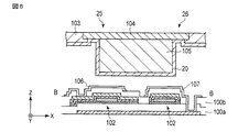
図4は図3に示す土台部27のA−A断面図を示す。TFT基板には、TFT2が形成されている。このTFT2は、例えばアルミニウム、クロム又はモリブデンからなるゲート膜と、例えばシリコン窒化膜からなるゲート絶縁膜100aと、例えば真性アモルファスシリコンからなる真性シリコン膜と、例えばシリコン窒化膜からなるチャネル保護膜と、例えばnアモルファスシリコンからなるnシリコン膜と、例えばアルミニウム、クロム又はモリブデンからなるソース・ドレイン膜と、例えばシリコン窒化膜からなるオーバーコート絶縁膜100bとを積層して形成されている。 FIG. 4 is a cross-sectional view of the base portion 27 shown in FIG. A TFT 2 is formed on the TFT substrate. The TFT 2 includes a gate film made of, for example, aluminum, chromium, or molybdenum, a gate insulating film 100a made of, for example, a silicon nitride film, an intrinsic silicon film made of, for example, intrinsic amorphous silicon, and a channel protective film made of, for example, a silicon nitride film, For example, an n + silicon film made of n + amorphous silicon, a source / drain film made of, for example, aluminum, chromium or molybdenum, and an overcoat insulating film 100b made of, for example, a silicon nitride film are laminated.

一方、カラーフィルタ基板には、カラーフィルタ103と、ブラックマトリックス104と、複数の接点用突起部105とが設けられている。これら接点用突起105は、それぞれX座標検知部25、Y座標検知部26及び土台部27の各部分に対峙して設けられている。これら接点用突起部105、カラーフィルタ103及びブラックマトリックス104上には、対向電極20が設けられている。   On the other hand, the color filter substrate is provided with a color filter 103, a black matrix 104, and a plurality of contact protrusions 105. These contact projections 105 are provided to face the X coordinate detection unit 25, the Y coordinate detection unit 26, and the base unit 27, respectively. A counter electrode 20 is provided on the contact protrusions 105, the color filter 103, and the black matrix 104.

土台部27は、オーバーコート絶縁膜100b上に画素電極1と同じ材料、例えばITOを使用して電極108が形成され、さらに例えばシリコン窒化膜からなる絶縁体の高さ調整部11aを形成して配置されている。接点用突起部105は、柱状スペーサの役割を果たして高さ調整部11aに接触している。これにより、外部からの押圧を受けていないときのX座標検知部25とY座標検知部26との各接点間隔は、予め設定された同じ接点間隔に設定される。   The base portion 27 is formed by forming an electrode 108 on the overcoat insulating film 100b using the same material as the pixel electrode 1, for example, ITO, and further forming an insulator height adjusting portion 11a made of, for example, a silicon nitride film. Has been placed. The contact protrusion 105 serves as a columnar spacer and contacts the height adjusting portion 11a. Thereby, each contact space | interval of the X coordinate detection part 25 when not receiving the press from the outside and the Y coordinate detection part 26 is set to the same preset contact space | interval.

図5はX座標検知部25及びY座標検知部26の周辺部の平面構成図を示す。上記同様に、複数の画素電極1の横方向における各間には、図面上の左側から右側の方向に向かって順次、1本のデータ配線3、X座標検知配線4、2本のデータ配線3が繰り返し配置されている。X座標検知部25及びY座標検知部26は、一対で、X座標検知配線4とY座標検知配線7との交差部分上で、かつY方向において、2つの画素電極1毎に配置されている。   FIG. 5 is a plan configuration diagram of the periphery of the X coordinate detection unit 25 and the Y coordinate detection unit 26. Similarly to the above, between each of the plurality of pixel electrodes 1 in the horizontal direction, one data wiring 3, X coordinate detection wiring 4, and two data wirings 3 are sequentially arranged from the left side to the right side in the drawing. Are arranged repeatedly. A pair of the X coordinate detection unit 25 and the Y coordinate detection unit 26 are arranged for each of the two pixel electrodes 1 on the intersection of the X coordinate detection wiring 4 and the Y coordinate detection wiring 7 and in the Y direction. .

各TFT2の横方向における配置位置は、画素電極1に対して右側又は左側に配置される。例えば、図5の図面上において、最も左側に配置された画素電極1とその右側に隣接する画素電極1との間には、X座標検知配線4が配置されている。かかる最も左側に配置された画素電極1に対してTFT2は、当該画素電極1における下端辺の左側に配置される。次に右側に隣接する画素電極1に対してTFT2は、当該画素電極1における下端辺の右側に配置される。これにより、X座標検知配線4の左右両側に配置されている各TFT2の横方向の間隔は、図17に示す各TFT2の横方向の間隔よりも広く形成される。
このX座標検知配線4の左右両側に配置されている各TFT2の横方向の間隔は、一対のX座標検知部25及びY座標検知部26の横方向の長さよりも長い。従って、一対のX座標検知部25及びY座標検知部26は、縦方向上でTFT2と共に配列されずに、横方向の各TFT2の間に配置することが可能であり、各画素電極1の縦方向の間隔を図17に示す従来の各画素電極1の縦方向の間隔よりも狭くすることができる。
The arrangement position of each TFT 2 in the horizontal direction is arranged on the right side or the left side with respect to the pixel electrode 1. For example, in the drawing of FIG. 5, the X coordinate detection wiring 4 is arranged between the pixel electrode 1 arranged on the leftmost side and the pixel electrode 1 adjacent to the right side thereof. The TFT 2 is arranged on the left side of the lower end side of the pixel electrode 1 with respect to the pixel electrode 1 arranged on the leftmost side. Next, the TFT 2 is disposed on the right side of the lower end side of the pixel electrode 1 with respect to the pixel electrode 1 adjacent to the right side. Thereby, the horizontal interval between the TFTs 2 arranged on the left and right sides of the X coordinate detection wiring 4 is formed wider than the horizontal interval between the TFTs 2 shown in FIG.
The horizontal distance between the TFTs 2 arranged on the left and right sides of the X coordinate detection wiring 4 is longer than the horizontal length of the pair of X coordinate detection unit 25 and Y coordinate detection unit 26. Therefore, the pair of the X coordinate detection unit 25 and the Y coordinate detection unit 26 can be arranged between the TFTs 2 in the horizontal direction without being arranged together with the TFTs 2 in the vertical direction, and the vertical direction of each pixel electrode 1 can be arranged. The interval in the direction can be made narrower than the interval in the vertical direction of each conventional pixel electrode 1 shown in FIG.

図6は図5に示すX座標検知部25及びY座標検知部26のB−B断面図を示す。X座標検知部25は、オーバーコート絶縁膜100b上に画素電極と同じ材料、例えばITOを使用してX座標検知接点電極107が形成されている。このX座標検知接点電極107は、積層構造102中のX座標検知配線4に接続されている。これにより、X座標検知部25は、外部からの押圧を受けて対向電極20とX座標検知接点電極107とが導通すると、X座標検知配線4にX座標信号を生成する。
Y座標検知部26は、オーバーコート絶縁膜100b上に画素電極と同じ材料、例えばITOを使用してY座標検知接点電極106が形成されている。このY座標検知接点電極106は、積層構造102中のY座標検知配線7に接続されている。これにより、Y座標検知部26は、外部からの押圧を受けて対向電極20とY座標検知接点電極106とが導通すると、Y座標検知配線7にY座標信号を生成する。
FIG. 6 is a cross-sectional view taken along the line BB of the X coordinate detection unit 25 and the Y coordinate detection unit 26 shown in FIG. In the X coordinate detection unit 25, an X coordinate detection contact electrode 107 is formed on the overcoat insulating film 100b using the same material as the pixel electrode, for example, ITO. The X coordinate detection contact electrode 107 is connected to the X coordinate detection wiring 4 in the laminated structure 102. As a result, the X coordinate detection unit 25 generates an X coordinate signal in the X coordinate detection wiring 4 when the counter electrode 20 and the X coordinate detection contact electrode 107 are electrically connected by receiving an external pressure.
In the Y coordinate detection unit 26, the Y coordinate detection contact electrode 106 is formed on the overcoat insulating film 100b using the same material as the pixel electrode, for example, ITO. The Y coordinate detection contact electrode 106 is connected to the Y coordinate detection wiring 7 in the laminated structure 102. As a result, the Y coordinate detection unit 26 generates a Y coordinate signal in the Y coordinate detection wiring 7 when the counter electrode 20 and the Y coordinate detection contact electrode 106 are electrically connected to each other by receiving external pressure.

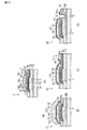
次に、図7乃至図11を参照して第1の基板(TFT基板)上におけるTFT2、X座標検知部25、Y座標検知部26、土台部27に共通の作成工程について詳しく説明する。
なお、図7乃至図11の各分図(A)は、それぞれ図3に示すIVA−IVA部分においてTFT2が順次形成される様子の断面図を示す。
図7乃至図11の各分図(B)は、それぞれ図3に示すA−A(IVB−IVB)部分においてTFT2の作成と同時に順次形成される土台部27の様子の断面図を示す。
図7乃至図11の各分図(C)は、それぞれ図5に示すIVC−IVC部分においてTFT2の作成と同時に順次形成されるX座標検知部25の様子の断面図を示す。
図7乃至図11の各分図(D)は、それぞれ図5に示すIVD−IVD部分においてTFT2の作成と同時に順次形成されるY座標検知部26の様子の断面図を示す。
最初、図7(A)〜(D)に示すようにTFT2、土台部27、X座標検知部25、Y座標検知部26に対応する各部分には、第1基板(TFT基板)上にフォトリソグラフィ法により、例えばアルミニウム、クロム又はモリブデンからなるゲート膜を使用してゲート配線5及びゲート配線5に沿い延伸しているY座標検知配線7が形成される。そして、ゲート配線5においてTFT2に対応した部分はTFT2のためのゲート電極5cを提供している。またY座標検知配線7においてY座標検知部26に対応した部分は、当該Y座標検知部26のための接続部分7bを提供している。
Next, with reference to FIG. 7 to FIG. 11, a production process common to the TFT 2, the X coordinate detection unit 25, the Y coordinate detection unit 26, and the base unit 27 on the first substrate (TFT substrate) will be described in detail.
Each of FIGS. 7A to 11A is a sectional view showing a state in which the TFTs 2 are sequentially formed in the IVA-IVA portion shown in FIG.
Each of FIGS. 7 to 11 (B) is a sectional view showing the state of the base portion 27 that is sequentially formed simultaneously with the creation of the TFT 2 in the AA (IVB-IVB) portion shown in FIG.
Each of FIG. 7 to FIG. 11C is a cross-sectional view of the state of the X coordinate detection unit 25 that is sequentially formed simultaneously with the creation of the TFT 2 in the IVC-IVC portion shown in FIG.
Each of FIG. 7 to FIG. 11D is a cross-sectional view of the state of the Y coordinate detection unit 26 that is sequentially formed simultaneously with the creation of the TFT 2 in the IVD-IVD portion shown in FIG.
First, as shown in FIGS. 7A to 7D, each portion corresponding to the TFT 2, the base portion 27, the X coordinate detection portion 25, and the Y coordinate detection portion 26 has a photo on the first substrate (TFT substrate). The gate wiring 5 and the Y coordinate detection wiring 7 extending along the gate wiring 5 are formed by lithography using a gate film made of, for example, aluminum, chromium, or molybdenum. A portion of the gate wiring 5 corresponding to the TFT 2 provides a gate electrode 5 c for the TFT 2. Further, the portion corresponding to the Y coordinate detection unit 26 in the Y coordinate detection wiring 7 provides a connection portion 7 b for the Y coordinate detection unit 26.

次に、図8(A)〜(D)に示すようにTFT2、土台部27、X座標検知部25、Y座標検知部26に対応する各部分には、第1基板(TFT基板)上に例えばシリコン窒化膜(SiNx)を使用した透明なゲート絶縁膜100がゲート配線5及びY座標検知配線7を覆うよう形成される。
次に、例えば真性アモルファスシリコンからなるa−Si層52及び例えばnアモルファスシリコンからなるna−Si層54が、部分的に例えばSiNxを使用したチャネル保護膜56を間に介して、積層される。
Next, as shown in FIGS. 8A to 8D, the portions corresponding to the TFT 2, the base portion 27, the X coordinate detection portion 25, and the Y coordinate detection portion 26 are placed on the first substrate (TFT substrate). For example, a transparent gate insulating film 100 using a silicon nitride film (SiNx) is formed so as to cover the gate wiring 5 and the Y coordinate detection wiring 7.
Next, an a-Si layer 52 made of, for example, intrinsic amorphous silicon and an n + a-Si layer 54 made of, for example, n + amorphous silicon are stacked with a channel protective film 56 partially using, for example, SiNx interposed therebetween. Is done.

次に、na−Si層54を覆うように例えばアルミニウム、クロム又はモリブデンからなるソース・ドレイン膜58が形成される。ソース・ドレイン膜58は、TFT2の近傍のデータ配線3及びX座標検知部25の近傍のX座標検知配線4を提供している。そして、X座標検知配線4においてX座標検知部25に対応した部分は、当該X座標検知部25のための接続部分25bを提供している。
a−Si層54及びソース・ドレイン膜58は、図8(A)中に示されているように、画素電極1に近い側と画素電極1から遠い側とで2分割される。
a−Si層52、チャネル保護膜56,そしてこの様に2分割されたna−Si層54の積層の組み合わせは、TFT2のオーミックス層24dを提供している。また、このように2分割されたソース・ドレイン膜58は、画素電極1に近い側がTFT2のソース電極24aを、また画素電極1から遠い側がTFT2においてデータ配線3から延びているドレイン電極24bを提供している。
Next, a source / drain film 58 made of, for example, aluminum, chromium, or molybdenum is formed so as to cover the n + a-Si layer 54. The source / drain film 58 provides the data wiring 3 near the TFT 2 and the X coordinate detection wiring 4 near the X coordinate detection unit 25. The portion corresponding to the X coordinate detection unit 25 in the X coordinate detection wiring 4 provides a connection portion 25 b for the X coordinate detection unit 25.
As shown in FIG. 8A, the n + a-Si layer 54 and the source / drain film 58 are divided into two on the side close to the pixel electrode 1 and the side far from the pixel electrode 1.
The laminated combination of the a-Si layer 52, the channel protective film 56, and the n + a-Si layer 54 divided in this way provides the ohmics layer 24d of the TFT2. Further, the source / drain film 58 divided in two provides the source electrode 24a of the TFT 2 on the side close to the pixel electrode 1, and the drain electrode 24b extending from the data wiring 3 in the TFT 2 on the side far from the pixel electrode 1. doing.

次に、図9(A)〜(D)に示すようにTFT2、土台部27、X座標検知部25、Y座標検知部26に対応する各部分には、ソース・ドレイン膜58を覆う例えばシリコン窒化膜(SiNx)を使用した透明なオーバーコート絶縁膜101が形成される。
ここで、図9(A)中に図示されているように、オーバーコート絶縁膜101においてTFT2の対応部分においては、ソース・ドレイン膜58のソース電極24aに対応した位置にソース電極24aを露出させるためのコンタクトホール101aが形成される。
Next, as shown in FIGS. 9A to 9D, the portions corresponding to the TFT 2, the base portion 27, the X coordinate detection portion 25, and the Y coordinate detection portion 26 are covered with a source / drain film 58 such as silicon. A transparent overcoat insulating film 101 using a nitride film (SiNx) is formed.
Here, as shown in FIG. 9A, in the portion corresponding to the TFT 2 in the overcoat insulating film 101, the source electrode 24a is exposed at a position corresponding to the source electrode 24a of the source / drain film 58. Contact hole 101a is formed.

また、図9(C)中に示すようにオーバーコート絶縁膜101においてX座標検知配線4のX座標検知部25のための接続部分25bに対応した部分に、当該接続部分25bを露出させるためのコンタクトホール101bが形成されている。   Further, as shown in FIG. 9C, in the overcoat insulating film 101, the connection portion 25b is exposed at a portion corresponding to the connection portion 25b for the X coordinate detection portion 25 of the X coordinate detection wiring 4. A contact hole 101b is formed.

さらに、図9(D)中に図示されているように、オーバーコート絶縁膜101においてY座標検知配線7のY座標検知部26のための接続部分26bに対応した部分に、当該接続部分26bを露出させるためのコンタクトホール101cが形成される。コンタクトホール101cは、オーバーコート絶縁膜101とY座標検知部26のための接続部分26bとの間に存在しているゲート絶縁膜100も貫通している。   Further, as shown in FIG. 9D, the connection portion 26b is formed in a portion corresponding to the connection portion 26b for the Y coordinate detection portion 26 of the Y coordinate detection wiring 7 in the overcoat insulating film 101. A contact hole 101c for exposure is formed. The contact hole 101 c also penetrates the gate insulating film 100 that exists between the overcoat insulating film 101 and the connection portion 26 b for the Y coordinate detection unit 26.

この段階で、図9(A)中に図示されているTFT2の対応部分においては、ゲート配線5によるゲート電極5c、ゲート電極5cに重なったゲート絶縁膜100の部分、ゲート絶縁膜100の前記部分に重なった、a−Si層52、チャネル保護膜56、そして2分割されたna−Si膜54を含む半導体のためのオーミックス層24d、オーミックス層24dの2分割されたna−Si膜54上のソース電極24a及びドレイン電極24b、そしてソース電極24a及びドレイン電極24bを覆うオーバーコート絶縁膜101が、TFT2を提供している。 At this stage, in the corresponding portion of the TFT 2 shown in FIG. 9A, the gate electrode 5c by the gate wiring 5, the portion of the gate insulating film 100 overlapping the gate electrode 5c, and the portion of the gate insulating film 100 It overlaps the, a-Si layer 52, the channel protection film 56, and two divided n + a-Si film 54 O mix layer 24d for semiconductor including two split n + a Haut mix layer 24d The TFT 2 is provided by the source electrode 24a and the drain electrode 24b on the Si film 54 and the overcoat insulating film 101 covering the source electrode 24a and the drain electrode 24b.

次に、図10(A)〜(D)に示すようにTFT2、土台部27、X座標検知部25、Y座標検知部26、土台部27に対応する各部分には、オーバーコート絶縁膜101を覆うよう例えばITOからなる透明導電膜62が形成される。
透明導電膜62は、図10(A)中に示すように、ソース電極24aを露出させるためのコンタクトホール101a中にも形成されてソース電極24aと電気的に接続される。透明導電膜62は、図10(C)中に示すように、X座標検知部25のための接続部分25bを露出させるためのコンタクトホール101b中にも形成されて当該接続部分25bと電気的に接続される。透明導電膜62はさらに、図10(D)中に示すように、Y座標検知部26のための接続部分26bを露出させるためのコンタクトホール101c中にも形成されて当該接続部分26bと電気的に接続される。
Next, as shown in FIGS. 10A to 10D, the overcoat insulating film 101 is formed on the portions corresponding to the TFT 2, the base portion 27, the X coordinate detection portion 25, the Y coordinate detection portion 26, and the base portion 27. A transparent conductive film 62 made of, for example, ITO is formed so as to cover the surface.
As shown in FIG. 10A, the transparent conductive film 62 is also formed in the contact hole 101a for exposing the source electrode 24a and is electrically connected to the source electrode 24a. As shown in FIG. 10C, the transparent conductive film 62 is also formed in the contact hole 101b for exposing the connection portion 25b for the X coordinate detection unit 25, and is electrically connected to the connection portion 25b. Connected. Further, as shown in FIG. 10D, the transparent conductive film 62 is also formed in the contact hole 101c for exposing the connection portion 26b for the Y coordinate detection unit 26 and is electrically connected to the connection portion 26b. Connected to.

透明導電膜62が形成された時点で、図10(A)〜(D)中に示すようにTFT2の断面の一部、土台部27の断面の一部、X座標検知部25の断面の一部、そしてY座標検知部26の断面の一部のそれぞれは、TFT2を形成するための前述した作成方法よって第1基板(TFT基板)上に共通して同時に形成されているので、第1基板(TFT基板)上からの高さは相互に同じである。   When the transparent conductive film 62 is formed, as shown in FIGS. 10A to 10D, a part of the cross section of the TFT 2, a part of the cross section of the base part 27, and a cross section of the X coordinate detection part 25. And a part of the cross section of the Y-coordinate detection unit 26 are simultaneously formed on the first substrate (TFT substrate) by the above-described production method for forming the TFT 2. (TFT substrate) The height from above is the same.

次に、土台部27の断面の一部を示している図10(B)においては、透明導電膜62の上にさらに、所定の高さの例えばシリコン窒化膜(SiNx)を使用した透明な土台部絶縁膜により高さ調整部27aが形成され、その頂点が土台部27の突出端面(先端)27bを提供している。   Next, in FIG. 10B showing a part of the cross section of the base portion 27, a transparent base using, for example, a silicon nitride film (SiNx) having a predetermined height on the transparent conductive film 62. A height adjusting portion 27 a is formed by the partial insulating film, and the apex thereof provides a protruding end surface (tip) 27 b of the base portion 27.

最後に透明導電膜62は、TFT2の対応部分では図11(A)中に示すように、ソース電極24aと電気的に接続されたコンタクトホール101a中の部分及びTFT2に隣接した画素電極1を提供する部分を除き削除される。
また最後に透明導電膜62は、土台部27の対応部分では図11(B)中に示すように、高さ調整部27aに覆われている部分108を除き削除される。
また、最後に透明導電膜62は、X座標検知部25の対応部分及びX座標検知配線4の接続部分4bにおいて図11(C)中に示すように、X座標検知接点電極106を提供するX座標検知部25の対応部分、及び当該X座標検知部25をX座標検知配線4の接続部分4bに電気的に接続させるコンタクトホール101b中の部分を除き削除される。
さらに最後に透明導電膜62は、Y座標検知部26の対応部分及びY座標検知配線7の接続部分7bにおいて図11(D)中に示すように、Y座標検知接点電極107を提供するY座標検知部26の対応部分、及び当該Y座標検知部26をY座標検知配線7の接続部分7bに電気的に接続させるコンタクトホール101c中の部分を除き除去される。
図11(A)〜(D)に示すTFT2、土台部27、X座標検知部25、Y座標検知部26に対応する各部分を対比すると、第1基板(TFT基板)から図11(C)に示すX座標検知部25の突出端面(先端)までの高さ及び図11(D)に示すY座標検知部26の突出端面(先端)までの高さは相互に同じである。
第1基板(TFT基板)から図11(A)に示すTFT2の突出端面(先端)までの高さは、図11(C)に示す前述したX座標検知部25の突出端面(先端)までの高さ及び図11(D)に示すY座標検知部26の突出端面(先端)までの高さよりも、最後にTFT2の突出端面(先端)から除去された透明導電膜62の厚さ分だけ低い。
さらに、第1基板(TFT基板)から土台部27の突出端面(先端)27bまでの高さは、図11(C)に示す前述したX座標検知部25の突出端面(先端)までの高さ及び図11(D)に示すY座標検知部26の突出端面(先端)までの高さよりも、最後に透明導電膜62の上に形成された高さ調整部27aの突出端面(先端)27bまでの高さ分だけ高い。
Finally, as shown in FIG. 11A, the transparent conductive film 62 provides a portion in the contact hole 101a electrically connected to the source electrode 24a and the pixel electrode 1 adjacent to the TFT 2 at the corresponding portion of the TFT 2. It is deleted except the part to do.
Finally, the transparent conductive film 62 is deleted except for the portion 108 covered with the height adjusting portion 27a in the corresponding portion of the base portion 27 as shown in FIG.
Finally, the transparent conductive film 62 provides an X coordinate detection contact electrode 106 as shown in FIG. 11C at the corresponding portion of the X coordinate detection unit 25 and the connection portion 4b of the X coordinate detection wiring 4. The corresponding part of the coordinate detection unit 25 and the part in the contact hole 101b that electrically connects the X coordinate detection unit 25 to the connection part 4b of the X coordinate detection wiring 4 are deleted.
Finally, the transparent conductive film 62 provides the Y coordinate detection contact electrode 107 as shown in FIG. 11D at the corresponding portion of the Y coordinate detection unit 26 and the connection portion 7b of the Y coordinate detection wiring 7. The corresponding portion of the detection unit 26 and the portion in the contact hole 101c that electrically connects the Y coordinate detection unit 26 to the connection portion 7b of the Y coordinate detection wiring 7 are removed.
Comparing each portion corresponding to the TFT 2, the base portion 27, the X coordinate detection portion 25, and the Y coordinate detection portion 26 shown in FIGS. 11A to 11D, the first substrate (TFT substrate) to FIG. The height to the protruding end surface (tip) of the X coordinate detection unit 25 shown in FIG. 11 is the same as the height to the protruding end surface (tip) of the Y coordinate detection unit 26 shown in FIG.
The height from the first substrate (TFT substrate) to the protruding end surface (tip) of the TFT 2 shown in FIG. 11A is from the protruding end surface (tip) of the X coordinate detector 25 shown in FIG. 11C. It is lower than the height and the height to the protruding end face (tip) of the Y coordinate detector 26 shown in FIG. 11D by the thickness of the transparent conductive film 62 finally removed from the protruding end face (tip) of the TFT 2. .
Further, the height from the first substrate (TFT substrate) to the protruding end surface (tip) 27b of the base portion 27 is the height to the protruding end surface (tip) of the X-coordinate detection unit 25 described above shown in FIG. 11D, until the protruding end surface (tip) 27b of the height adjusting unit 27a finally formed on the transparent conductive film 62 is higher than the height to the protruding end surface (tip) of the Y coordinate detection unit 26 shown in FIG. Higher than the height of

このように上記第1の実施の形態によれば、複数の画素電極1の横方向(X方向)における各間に、例えば1本のデータ配線3、X座標検知配線4、2本のデータ配線3を繰り返し配置するので、これら1本のデータ配線3と2本のデータ配線3との配置位置によって画素電極1に対する各TFT2の横方向における配置位置を当該画素電極1に対して右側又は左側に配置するものとなる。かかる各TFT2の配置により、X座標検知配線4の左右両側に配置されている各TFT2の横方向の間隔を図15に示す従来の各TFT2の横方向の間隔よりも広く形成することができる。このX座標検知配線4の左右両側に配置されている各TFT2の横方向の間隔は、土台部27の横方向の長さや、並設された一対のX座標検知部25とY座標検知部26との横方向の長さよりも長くできる。従って、土台部27と一対のX座標検知部25及びY座標検知部26とは、それぞれ横方向の各TFT2の間に詰めて配置することが可能である。この結果、各画素電極1の縦方向の間隔は、図15に示す従来の各画素電極1の縦方向の間隔よりも狭くすることができる。   As described above, according to the first embodiment, for example, one data wiring 3, X coordinate detection wiring 4, and two data wirings are provided between the plurality of pixel electrodes 1 in the horizontal direction (X direction). 3 is repeatedly arranged, the horizontal arrangement position of each TFT 2 with respect to the pixel electrode 1 is set to the right side or the left side with respect to the pixel electrode 1 depending on the arrangement position of the one data line 3 and the two data lines 3. It will be placed. With the arrangement of the TFTs 2, the horizontal intervals of the TFTs 2 arranged on the left and right sides of the X coordinate detection wiring 4 can be formed wider than the horizontal intervals of the conventional TFTs 2 shown in FIG. 15. The horizontal interval between the TFTs 2 arranged on the left and right sides of the X coordinate detection wiring 4 is the horizontal length of the base portion 27 and a pair of X coordinate detection unit 25 and Y coordinate detection unit 26 arranged in parallel. It can be longer than the horizontal length. Therefore, the base portion 27 and the pair of X coordinate detection portion 25 and Y coordinate detection portion 26 can be arranged between the respective TFTs 2 in the horizontal direction. As a result, the vertical interval between the pixel electrodes 1 can be made narrower than the vertical interval between the conventional pixel electrodes 1 shown in FIG.

すなわち、縦方向(Y方向)においてTFT2と、X座標検知部25及びY座標検知部26と、土台部27と、をY方向に詰めて配列することができ、同縦方向(Y方向)における各画素電極1の間隔を狭くすることができる。この結果、各画素電極1の間隔を狭くした長さに相当する分だけ本装置100としての開口率を大きくすることができ、本装置100の表示性能、例えば表示の輝度等の画質を向上することが出来る。   That is, in the vertical direction (Y direction), the TFT 2, the X coordinate detection unit 25, the Y coordinate detection unit 26, and the base unit 27 can be arranged in the Y direction and arranged in the same vertical direction (Y direction). The interval between the pixel electrodes 1 can be reduced. As a result, the aperture ratio of the apparatus 100 can be increased by an amount corresponding to the length in which the interval between the pixel electrodes 1 is narrowed, and the display performance of the apparatus 100, for example, the image quality such as display brightness is improved. I can do it.

本装置100と従来装置とを比較すると、図12に示すように本装置100の画素電極1間のY方向の間隔Laは、従来装置の画素電極1間の間隔Lbよりも狭く形成されている(La<Lb)。従って、本装置100の各画素電極1のY方向の長さは、従来装置の各画素電極1のY方向の長さよりも長く形成することができる。これにより、本装置100の各画素電極1の面積Saは、従来装置の各画素電極1の面積Sbよりも広くすることが出来る(Sa>Sb)。
本装置100の各画素電極1のX方向の長さは、従来装置の各画素電極1の同方向の長さと同一であるものの、各画素電極1のY方向の長さは、本装置100の方が従来装置よりも長くなっている。これにより、本装置100の各画素電極1の面積Saは、従来装置の各画素電極1の面積Sbよりも広くなっている。
Comparing the device 100 with the conventional device, as shown in FIG. 12, the interval La between the pixel electrodes 1 of the device 100 is formed narrower than the interval Lb between the pixel electrodes 1 of the conventional device. (La <Lb). Therefore, the length of each pixel electrode 1 of the device 100 in the Y direction can be formed longer than the length of each pixel electrode 1 of the conventional device in the Y direction. Thereby, the area Sa of each pixel electrode 1 of the device 100 can be made larger than the area Sb of each pixel electrode 1 of the conventional device (Sa> Sb).
Although the length in the X direction of each pixel electrode 1 of the device 100 is the same as the length in the same direction of each pixel electrode 1 of the conventional device, the length in the Y direction of each pixel electrode 1 is the same as that of the device 100. It is longer than the conventional device. As a result, the area Sa of each pixel electrode 1 of the apparatus 100 is larger than the area Sb of each pixel electrode 1 of the conventional apparatus.

例えば、図2においてX座標検知部25及びY座標検知部26は、4つの土台部27の配置位置を各コーナとする正四辺形Wの中央部に配置されている。X座標検知部25及びY座標検知部26の配置位置は、タッチ操作による外部からの押圧を受けたときに対向電極20に生じる湾曲の量が最大となるところである。すなわち、正四辺形W内で対向電極20が最も湾曲しやすいところであり、タッチ操作による僅かな押圧によってX座標検知部25及びY座標検知部26は、それぞれXY座標信号を生成することができる。すなわち、タッチ操作を受けてのX座標及びY座標検知の感度を高くできる。   For example, in FIG. 2, the X coordinate detection unit 25 and the Y coordinate detection unit 26 are arranged at the center of a regular quadrilateral W having the arrangement positions of the four base parts 27 as corners. The arrangement position of the X coordinate detection unit 25 and the Y coordinate detection unit 26 is where the amount of bending that occurs in the counter electrode 20 is maximized when an external pressure is applied by a touch operation. That is, the counter electrode 20 is most easily curved in the regular quadrilateral W, and the X coordinate detection unit 25 and the Y coordinate detection unit 26 can generate XY coordinate signals by a slight press by a touch operation. That is, the sensitivity of X coordinate and Y coordinate detection upon receiving a touch operation can be increased.

[第2の実施の形態]
次に、本発明の第2の実施の形態について図面を参照して説明する。なお、図2と同一部分には同一符号を付してその詳しい説明は省略する。
図13はタッチパネル機能を有する液晶表示装置の構成図を示す。本装置100は、各画素電極1のX方向における間には、図面上の左側から右側方向に順次、2本のデータ配線3、その右隣の間にX座標検知配線4、さらにその右隣の間に1本のデータ配線3、の順序で繰り返し配置されている。
[Second Embodiment]
Next, a second embodiment of the present invention will be described with reference to the drawings. The same parts as those in FIG. 2 are denoted by the same reference numerals, and detailed description thereof is omitted.
FIG. 13 shows a configuration diagram of a liquid crystal display device having a touch panel function. The apparatus 100 includes two data lines 3 in order from the left side to the right side of the drawing between the pixel electrodes 1 in the X direction, an X coordinate detection line 4 between the right side and the right side. Are arranged repeatedly in the order of one data wiring 3.

このような2本のデータ配線3と、X座標検知配線4と、1本のデータ配線3との配置順序であれば、上記第1の実施の形態と同様に、X座標検知配線4の左右両側に配置されている各TFT2の横方向の間隔を図15に示す従来の各TFT2の横方向の間隔よりも広く形成することができ、これらTFT2の横方向の間内に、一対のX座標検知部25及びY座標検知部26と、土台部27とをY方向に詰めて配列することができ、Y方向における各画素電極1の間隔を狭くすることができる。
この結果、各画素電極1の間隔を狭くした長さに相当する分だけ本装置100としての開口率を大きくすることができ、本装置100の表示性能、例えば表示の輝度等の画質を向上することが出来る等、上記第1の実施の形態と同様の効果を奏することができる。
If the arrangement order of the two data wirings 3, the X coordinate detection wiring 4 and the one data wiring 3 is as described above, the left and right sides of the X coordinate detection wiring 4 are the same as in the first embodiment. The horizontal interval between the TFTs 2 arranged on both sides can be formed wider than the horizontal interval between the conventional TFTs 2 shown in FIG. The detection unit 25, the Y coordinate detection unit 26, and the base unit 27 can be arranged close to each other in the Y direction, and the interval between the pixel electrodes 1 in the Y direction can be reduced.
As a result, the aperture ratio of the apparatus 100 can be increased by an amount corresponding to the length in which the interval between the pixel electrodes 1 is narrowed, and the display performance of the apparatus 100, for example, the image quality such as display brightness is improved. For example, the same effects as those of the first embodiment can be obtained.

[第3の実施の形態]
次に、本発明の第3の実施の形態について図面を参照して説明する。なお、図2と同一部分には同一符号を付してその詳しい説明は省略する。
図14はタッチパネル機能を有する液晶表示装置の構成図を示す。本装置100は、各画素電極1のX方向における間には、図面上の左側から右側方向に順次、1本のデータ配線3、その右隣の間にX座標検知配線4、さらにその右隣の間に2本のデータ配線3、の順序で繰り返し配置されている
又、本装置100は、一対のX座標検知部25及びY座標検知部26をY方向に配線された1本のX座標検知配線4上に配置している。これと共に本装置100は、土台部27をY方向に配線された1本のX座標検知配線4上に配置している。そして、一対のX座標検知部25及びY座標検知部26と土台部27とは、X方向に配置された3つの画素電極1毎に交互に配置されている。
[Third Embodiment]
Next, a third embodiment of the present invention will be described with reference to the drawings. The same parts as those in FIG. 2 are denoted by the same reference numerals, and detailed description thereof is omitted.
FIG. 14 shows a configuration diagram of a liquid crystal display device having a touch panel function. In the present apparatus 100, in the X direction of each pixel electrode 1, one data wiring 3 is sequentially arranged from the left side to the right side in the drawing, the X coordinate detection wiring 4 is adjacent to the right side of the data electrode 3, and the right side thereof. The apparatus 100 is repeatedly arranged in the order of two data wirings 3. The apparatus 100 also has a single X coordinate in which a pair of X coordinate detection unit 25 and Y coordinate detection unit 26 are wired in the Y direction. It is arranged on the detection wiring 4. At the same time, the present apparatus 100 arranges the base portion 27 on one X coordinate detection wiring 4 wired in the Y direction. And a pair of X coordinate detection part 25 and Y coordinate detection part 26, and the base part 27 are alternately arrange | positioned for every three pixel electrodes 1 arrange | positioned in the X direction.

このような構成であれば、上記第1の実施の形態と同様に、X座標検知配線4の左右両側に配置されている各TFT2の横方向の間隔を図15に示す従来の各TFT2の横方向の間隔よりも広く形成することができ、これらTFT2の横方向の間内に、一対のX座標検知部25及びY座標検知部26と、土台部27とをY方向に詰めて配列することができ、Y方向における各画素電極1の間隔を狭くすることができる。
この結果、本装置100としての開口率を大きくすることができ、本装置100の表示性能、例えば表示の輝度等の画質を向上することが出来る等、上記第1の実施の形態と同様の効果を奏することができる。
With such a configuration, as in the first embodiment, the horizontal spacing between the TFTs 2 arranged on the left and right sides of the X coordinate detection wiring 4 is the horizontal width of each conventional TFT 2 shown in FIG. A pair of X coordinate detection unit 25 and Y coordinate detection unit 26, and a base unit 27 are arranged in the Y direction so as to be wider than the interval in the direction. The interval between the pixel electrodes 1 in the Y direction can be reduced.
As a result, the aperture ratio of the apparatus 100 can be increased, and the display performance of the apparatus 100, for example, the image quality such as the display brightness can be improved, and the same effects as in the first embodiment. Can be played.

なお、本発明は上記実施形態そのままに限定されるものではなく、実施段階ではその要旨を逸脱しない範囲で構成要素を変形して具体化できる。また、上記実施形態に開示されている複数の構成要素の適宜な組み合わせにより、種々の発明を形成できる。例えば、実施形態に示される全構成要素から幾つかの構成要素を削除してもよい。さらに、異なる実施形態にわたる構成要素を適宜組み合わせてもよい。   Note that the present invention is not limited to the above-described embodiment as it is, and can be embodied by modifying the constituent elements without departing from the scope of the invention in the implementation stage. In addition, various inventions can be formed by appropriately combining a plurality of components disclosed in the embodiment. For example, some components may be deleted from all the components shown in the embodiment. Furthermore, constituent elements over different embodiments may be appropriately combined.

100:本装置、1:画素電極、20:対向電極、Q:液晶層、2:薄膜トランジスタ(TFT)、21:データドライバ(データ駆動回路)、22:走査ドライバ(走査駆動回路)、23:X座標検出回路、24:Y座標検出部、3:データ配線、4:X座標検知配線、5:ゲート配線、25:X座標検知部、26:Y座標検知部、7:Y座標検知配線、27:土台部、6:補助容量配線、28:コンデンサ、3a:データ配線(データ配線延出部)、100a:ゲート絶縁膜、100b:オーバーコート絶縁膜、103:カラーフィルタ、104:ブラックマトリックス、105:接点用突起部、11a:高さ調整部、106:X座標検知接点電極、107:Y座標検知接点電極、102:積層構造。   100: This apparatus, 1: Pixel electrode, 20: Counter electrode, Q: Liquid crystal layer, 2: Thin film transistor (TFT), 21: Data driver (data drive circuit), 22: Scan driver (scan drive circuit), 23: X Coordinate detection circuit, 24: Y coordinate detection unit, 3: Data wiring, 4: X coordinate detection wiring, 5: Gate wiring, 25: X coordinate detection unit, 26: Y coordinate detection unit, 7: Y coordinate detection wiring, 27 : Base part, 6: Auxiliary capacitance wiring, 28: Capacitor, 3a: Data wiring (data wiring extension part), 100a: Gate insulating film, 100b: Overcoat insulating film, 103: Color filter, 104: Black matrix, 105 : Contact protrusion, 11a: height adjustment unit, 106: X coordinate detection contact electrode, 107: Y coordinate detection contact electrode, 102: laminated structure.

Claims (13)

第1の方向及び前記第1の方向とは異なる第2の方向にそれぞれ配列された複数の画素電極と、
前記複数の画素電極と対向配置された対向電極と、
前記複数の画素電極と前記対向電極との間に封入された液晶層と、
前記複数の画素電極にそれぞれ接続された複数の画素トランジスタと、
前記第1の方向に沿って配設された複数の第1の座標検知配線と、
前記第2の方向に沿って配設された複数の第2の座標検知配線と、
前記複数の画素用トランジスタに表示信号を供給する前記第2の方向に沿って配設された複数の信号線と、
それぞれ第1の接点を有し、前記複数の第1の座標検知配線にそれぞれ接続され、外部からの押圧を受けて前記第1の接点が前記対向電極に接触することにより前記対向電極と前記第1の座標検知配線とを導通させる複数の第1の座標検知部と、
それぞれ第2の接点を有し、前記複数の第2の座標検知配線にそれぞれ接続され、前記外部からの前記押圧を受けて前記第2の接点が前記対向電極に接触することにより当該対向電極と前記第2の座標検知配線とを導通させる複数の第2の座標検知部と、
を具備し、
前記第2の座標検知配線は、前記複数の画素電極のうち、前記第1の方向に連続して配列された第1の画素電極、第2の画素電極、第3の画素電極及び第4の画素電極における、前記第2の画素電極と前記第3の画素電極との間に配設され、
前記信号線は、前記第1の画素電極と前記第2の画素電極との間、前記第3の画素電極と前記第4の画素電極との間、のうちの一方の間に2本配設され、
前記第2の画素電極と前記第3の画素電極とには、前記画素トランジスタが前記第2の座標検知配線を挟んで前記第2の座標検知配線から離れる側に配置されてそれぞれ接続され、
前記第1の座標検知部及び前記第2の座標検知部は、前記第2の画素電極に接続された前記画素トランジスタと前記第3の画素電極に接続された前記画素トランジスタとの間に配置される、
ことを特徴とする液晶表示装置。
A plurality of pixel electrodes respectively arranged in a first direction and a second direction different from the first direction;
A counter electrode disposed opposite to the plurality of pixel electrodes,
A liquid crystal layer sealed between the plurality of pixel electrodes and the counter electrode;
A plurality of pixel transistors respectively connected to the plurality of pixel electrodes;
A plurality of first coordinate detection lines that are arranged along the first direction,
A plurality of second coordinate detection wires which are arranged along the second direction,
A plurality of signal lines disposed along the second direction for supplying a display signal to the plurality of pixel transistors;
Each of the first contacts has a first contact and is connected to each of the plurality of first coordinate detection wirings. When the first contact comes into contact with the counter electrode in response to an external pressure, the counter electrode and the first contact A plurality of first coordinate detection units for conducting a single coordinate detection wiring;
Each having a second contact, connected to each of the plurality of second coordinate detection wirings, and receiving the pressure from the outside, the second contact comes into contact with the counter electrode and A plurality of second coordinate detection units for conducting the second coordinate detection wiring;
Comprising
The second coordinate detection wiring includes a first pixel electrode, a second pixel electrode, a third pixel electrode, and a fourth pixel electrode that are continuously arranged in the first direction among the plurality of pixel electrodes. Disposed in the pixel electrode between the second pixel electrode and the third pixel electrode;
Two signal lines are arranged between one of the first pixel electrode and the second pixel electrode and between the third pixel electrode and the fourth pixel electrode. And
The pixel transistor is disposed on a side away from the second coordinate detection wiring with the second coordinate detection wiring interposed therebetween, and is connected to the second pixel electrode and the third pixel electrode, respectively.
The first coordinate detection unit and the second coordinate detection unit are disposed between the pixel transistor connected to the second pixel electrode and the pixel transistor connected to the third pixel electrode. The
A liquid crystal display device characterized by the above.
前記第1の座標検知部と前記第2の座標検知部とは、一対で配置されていることを特徴とする請求項1に記載の液晶表示装置。 The liquid crystal display device according to claim 1, wherein the first coordinate detection unit and the second coordinate detection unit are arranged in a pair . 前記第2の画素電極に接続された前記画素トランジスタと前記第3の画素電極に接続された前記画素トランジスタとの前記第1の方向の間隔は、前記一対の前記第1の座標検知部及び前記第2の座標検知部の前記第1の方向の長さよりも長いことを特徴とする請求項に記載の液晶表示装置。 The distance in the first direction between the pixel transistor connected to the second pixel electrode and the pixel transistor connected to the third pixel electrode is determined by the pair of the first coordinate detection units and The liquid crystal display device according to claim 2 , wherein a length of the second coordinate detection unit in the first direction is longer . 前記一対の前記第1の座標検知部及び前記第2の座標検知部は、前記第1の座標検知配線上に配置されていることを特徴とする請求項2又は3に記載の液晶表示装置。 4. The liquid crystal display device according to claim 2 , wherein the pair of the first coordinate detection unit and the second coordinate detection unit are arranged on the first coordinate detection wiring . 5. 前記複数の画素トランジスタに走査信号を供給する前記第1の方向に沿って配設された複数の走査線をさらに備え、
前記走査線は、前記画素電極と前記第1の座標検知配線の間に配置され、前記第1の座標検知配線に向かって前記走査線から張り出した張出部を有し、
前記画素トランジスタは、前記張出部がゲート電極になっていることを特徴とする請求項1乃至4の何れか1項に記載の液晶表示装置。
A plurality of scanning lines arranged along the first direction for supplying scanning signals to the plurality of pixel transistors;
The scanning line is disposed between the pixel electrode and the first coordinate detection wiring, and has a projecting portion that projects from the scanning line toward the first coordinate detection wiring.
5. The liquid crystal display device according to claim 1 , wherein the pixel transistor has the protruding portion serving as a gate electrode . 6.
前記複数の第1の座標検知部と前記対向電極との間隔及び前記複数の第2の座標検知部と前記対向電極との間隔をそれぞれ保持するスペーサと、前記押圧を受けていないときの前記第1の接点及び前記第2の接点と前記対向電極との間隔を予め設定された接点間隔に設定する複数の土台部と、をさらに備え、
前記第2の座標検知配線は、前記複数の画素電極のうち、前記第1の方向に連続して配列された第5の画素電極、第6の画素電極、第7の画素電極及び第8の画素電極における、前記第6の画素電極と前記第7の画素電極との間に配設され、
前記信号線は、前記第5の画素電極と前記第6の画素電極との間、前記第7の画素電極と前記第8の画素電極との間、のうちの一方の間に2本配設され、
前記第6の画素電極と前記第7の画素電極とには、前記画素トランジスタが前記第2の座標検知配線を挟んで前記第2の座標検知配線から離れる側に配置されてそれぞれ接続され、
前記土台部は、前記第6の画素電極に接続された前記画素トランジスタと前記第7の画素電極に接続された前記画素トランジスタとの間に配置されていることを特徴とする請求項1乃至5の何れか1項に記載の液晶表示装置。
Spacers that respectively hold the intervals between the plurality of first coordinate detection units and the counter electrode and the intervals between the plurality of second coordinate detection units and the counter electrode, and the first when not receiving the pressure A plurality of base portions for setting the interval between the first contact and the second contact and the counter electrode to a predetermined contact interval;
The second coordinate detection wiring includes, among the plurality of pixel electrodes, a fifth pixel electrode, a sixth pixel electrode, a seventh pixel electrode, and an eighth pixel that are continuously arranged in the first direction. Disposed in the pixel electrode between the sixth pixel electrode and the seventh pixel electrode;
Two signal lines are arranged between one of the fifth pixel electrode and the sixth pixel electrode and between the seventh pixel electrode and the eighth pixel electrode. And
The pixel transistor is disposed on a side away from the second coordinate detection wiring with the second coordinate detection wiring interposed therebetween, and is connected to the sixth pixel electrode and the seventh pixel electrode, respectively.
The base unit, according to claim 1 to 5, characterized in that it is disposed between the sixth the pixel transistor connected to said said pixel transistor seventh pixel electrode connected to the pixel electrode of the The liquid crystal display device according to any one of the above.
前記第6の画素電極に接続された前記画素トランジスタと前記第7の画素電極に接続された前記画素トランジスタとの前記第1の方向の間隔は、前記土台部の前記第1の方向の長さよりも長いことを特徴とする請求項6に記載の液晶表示装置。 The distance in the first direction between the pixel transistor connected to the sixth pixel electrode and the pixel transistor connected to the seventh pixel electrode is greater than the length of the base portion in the first direction. The liquid crystal display device according to claim 6, which is also long . 前記土台部は、前記第1の座標検知配線上に配置されていることを特徴とする請求項6又は7に記載の液晶表示装置。 The liquid crystal display device according to claim 6 , wherein the base portion is disposed on the first coordinate detection wiring . 前記複数の信号線と前記複数の第2の座標検知配線とは、前記複数の画素電極のうち、前記第1の方向に連続して配列された前記画素電極の連続した複数の間に、1本の前記信号線と1本の前記第2の座標検知配線と2本の前記信号線とが配置された配置順序、又は、2本の前記信号線と1本の前記第2の座標検知配線と1本の前記信号線とが配置された配置順序、で繰り返し配設されていることを特徴とする請求項6乃至8の何れか1項に記載の液晶表示装置。 The plurality of signal lines and the plurality of second coordinate detection wirings may be defined as 1 between the plurality of pixel electrodes continuously arranged in the first direction among the plurality of pixel electrodes. Arrangement order in which one signal line, one second coordinate detection wiring, and two signal lines are arranged, or two signal lines and one second coordinate detection wiring The liquid crystal display device according to claim 6 , wherein the liquid crystal display device is repeatedly arranged in an arrangement order in which a signal line and one signal line are arranged . 前記複数の第1の座標検知部及び前記複数の第2の座標検知部は、それぞれ一対であって前記第1の方向に沿って形成され、前記第1の座標検知配線と前記第2の座標検知配線との交差部分上で、前記第1の方向に沿った行に2つの前記交差部分毎に配置され、且つ、前記第2の方向に隣接する行毎に前記第1の方向に1つの前記交差部分だけずらして配置され、The plurality of first coordinate detection units and the plurality of second coordinate detection units are each paired and formed along the first direction, and the first coordinate detection wiring and the second coordinate are formed. On the intersecting portion with the detection wiring, it is arranged for each of the two intersecting portions in a row along the first direction, and one in the first direction for each row adjacent to the second direction. It is arranged by shifting only the intersection part,
前記複数の土台部は、前記第1の方向に沿って形成され、前記複数の第1の座標検知部及び前記複数の第2の座標検知部が配置された領域以外の前記交差部分上に配置されていることを特徴とする請求項9に記載の液晶表示装置。The plurality of base portions are formed along the first direction and arranged on the intersecting portion other than a region where the plurality of first coordinate detection units and the plurality of second coordinate detection units are arranged. The liquid crystal display device according to claim 9, wherein the liquid crystal display device is a liquid crystal display device.
前記複数の第1の座標検知部及び前記複数の第2の座標検知部は、それぞれ前記押圧を受けたときに前記対向電極に生じる湾曲の量が最大となるところに配置されていることを特徴とする請求項10に記載の液晶表示装置。The plurality of first coordinate detection units and the plurality of second coordinate detection units are respectively disposed where the amount of bending that occurs in the counter electrode is maximized when receiving the pressing. The liquid crystal display device according to claim 10. 第1の方向及び前記第1の方向とは異なる第2の方向にそれぞれ配列された複数の画素電極と、A plurality of pixel electrodes respectively arranged in a first direction and a second direction different from the first direction;
前記複数の画素電極と対向配置された対向電極と、A counter electrode disposed opposite to the plurality of pixel electrodes;
前記複数の画素電極にそれぞれ接続された複数の画素トランジスタと、A plurality of pixel transistors respectively connected to the plurality of pixel electrodes;
前記第1の方向に沿って配設された複数の第1の座標検知配線と、A plurality of first coordinate detection wirings arranged along the first direction;
前記第2の方向に沿って配設された複数の第2の座標検知配線と、A plurality of second coordinate detection wires arranged along the second direction;
前記複数の画素トランジスタに表示信号を供給する前記第2の方向に沿って配設された複数の信号線と、A plurality of signal lines disposed along the second direction for supplying display signals to the plurality of pixel transistors;
それぞれ第1の接点を有し、前記複数の第1の座標検知配線にそれぞれ接続され、外部からの押圧を受けて前記第1の接点が前記対向電極に接触することにより前記対向電極と前記第1の座標検知配線とを導通させる複数の第1の座標検知部と、Each of the first contacts has a first contact and is connected to each of the plurality of first coordinate detection wirings. When the first contact comes into contact with the counter electrode in response to an external pressure, the counter electrode and the first contact A plurality of first coordinate detection units for conducting a single coordinate detection wiring;
それぞれ第2の接点を有し、前記複数の第2の座標検知配線にそれぞれ接続され、前記外部からの前記押圧を受けて前記第2の接点が前記対向電極に接触することにより前記対向電極と前記第2の座標検知配線とを導通させる複数の第2の座標検知部と、Each having a second contact, connected to each of the plurality of second coordinate detection wirings, and receiving the pressure from the outside, the second contact comes into contact with the counter electrode, and A plurality of second coordinate detection units for conducting the second coordinate detection wiring;
前記複数の第1の座標検知部と前記対向電極との間隔及び前記複数の第2の座標検知部と前記対向電極との間隔をそれぞれ保持するスペーサを有し、前記押圧を受けていないときの前記第1の接点及び前記第2の接点と前記対向電極との間隔を予め設定された接点間隔に設定する複数の土台部と、When there is a spacer that holds the interval between the plurality of first coordinate detection units and the counter electrode and the interval between the plurality of second coordinate detection units and the counter electrode, and when the pressure is not received A plurality of base portions for setting a distance between the first contact and the second contact and the counter electrode to a predetermined contact distance;
を具備し、Comprising
前記第2の座標検知配線は、前記複数の画素電極のうち、前記第1の方向に連続して配列された第1の画素電極、第2の画素電極、第3の画素電極及び第4の画素電極における、前記第2の画素電極と前記第3の画素電極との間に配設され、The second coordinate detection wiring includes a first pixel electrode, a second pixel electrode, a third pixel electrode, and a fourth pixel electrode that are continuously arranged in the first direction among the plurality of pixel electrodes. Disposed in the pixel electrode between the second pixel electrode and the third pixel electrode;
前記信号線は、前記第1の画素電極と前記第2の画素電極との間、前記第3の画素電極と前記第4の画素電極との間、のうちの一方の間に2本配設されるとともに他方の間に1本配設され、Two signal lines are arranged between one of the first pixel electrode and the second pixel electrode and between the third pixel electrode and the fourth pixel electrode. And one is arranged between the other,
前記第2の画素電極と前記第3の画素電極とには、前記画素トランジスタが前記第2の座標検知配線を挟んで前記第2の座標検知配線から離れる側に配置されてそれぞれ接続され、The pixel transistor is disposed on a side away from the second coordinate detection wiring with the second coordinate detection wiring interposed therebetween, and is connected to the second pixel electrode and the third pixel electrode, respectively.
前記土台部、又は、前記第1の座標検知部及び前記第2の座標検知部は、前記第2の画素電極に接続された前記画素トランジスタと前記第3の画素電極に接続された前記画素トランジスタとの間に配置されていることを特徴とする液晶表示装置。The base unit, or the first coordinate detection unit and the second coordinate detection unit are the pixel transistor connected to the second pixel electrode and the pixel transistor connected to the third pixel electrode. A liquid crystal display device characterized by being disposed between the two.
前記第2の画素電極に接続された前記画素トランジスタと前記第3の画素電極に接続された前記画素トランジスタとの前記第1の方向の間隔は、前記第1の座標検知部及び前記第2の座標検知部の前記第1の方向の長さよりも長く、前記土台部の前記第1の方向の長さよりも長いことを特徴とする請求項12に記載の液晶表示装置。An interval in the first direction between the pixel transistor connected to the second pixel electrode and the pixel transistor connected to the third pixel electrode is determined by the first coordinate detector and the second The liquid crystal display device according to claim 12, wherein a length of the coordinate detection unit is longer than a length of the first direction and is longer than a length of the base portion of the first direction.
JP2010288851A 2010-12-24 2010-12-24 Liquid crystal display Expired - Fee Related JP5229312B2 (en)

Priority Applications (5)

Application Number Priority Date Filing Date Title
JP2010288851A JP5229312B2 (en) 2010-12-24 2010-12-24 Liquid crystal display
US13/335,136 US20120162109A1 (en) 2010-12-24 2011-12-22 Display apparatus
KR1020110139832A KR101389198B1 (en) 2010-12-24 2011-12-22 Display apparatus
TW100148185A TWI471640B (en) 2010-12-24 2011-12-23 A display apparatus
CN201110436903.0A CN102566819B (en) 2010-12-24 2011-12-23 Display apparatus

Applications Claiming Priority (1)

Application Number Priority Date Filing Date Title
JP2010288851A JP5229312B2 (en) 2010-12-24 2010-12-24 Liquid crystal display

Publications (3)

Publication Number Publication Date
JP2012137562A JP2012137562A (en) 2012-07-19
JP2012137562A5 JP2012137562A5 (en) 2012-11-15
JP5229312B2 true JP5229312B2 (en) 2013-07-03

Family

ID=46316046

Family Applications (1)

Application Number Title Priority Date Filing Date
JP2010288851A Expired - Fee Related JP5229312B2 (en) 2010-12-24 2010-12-24 Liquid crystal display

Country Status (5)

Country Link
US (1) US20120162109A1 (en)
JP (1) JP5229312B2 (en)
KR (1) KR101389198B1 (en)
CN (1) CN102566819B (en)
TW (1) TWI471640B (en)

Families Citing this family (10)

* Cited by examiner, † Cited by third party
Publication number Priority date Publication date Assignee Title
US9146644B2 (en) * 2010-03-08 2015-09-29 Nuvoton Technology Corporation Systems and methods for detecting multiple touch points in surface-capacitance type touch panels
US9030438B2 (en) * 2012-08-16 2015-05-12 Eastman Kodak Company Pixel-aligned micro-wire electrode device
US9098154B2 (en) * 2012-08-10 2015-08-04 Eastman Kodak Company Display apparatus with pixel-aligned micro-wire electrode
EP2713248B1 (en) 2012-09-28 2017-12-20 BlackBerry Limited Touch-sensitive display
CN103197480B (en) * 2013-03-22 2015-07-01 京东方科技集团股份有限公司 Array substrate and manufacture method thereof and display panel with same
CN103885637B (en) 2014-03-12 2017-05-31 京东方科技集团股份有限公司 A kind of In-cell touch panel and display device
KR101728627B1 (en) 2016-01-28 2017-04-19 호서대학교 산학협력단 Touch sensor
TWI581169B (en) * 2016-04-28 2017-05-01 友達光電股份有限公司 Dual-mode capacitive touch display panel
JP6322247B2 (en) * 2016-09-16 2018-05-09 Nissha株式会社 Pressure sensor
WO2018168682A1 (en) 2017-03-17 2018-09-20 シャープ株式会社 Display device with position input function

Family Cites Families (9)

* Cited by examiner, † Cited by third party
Publication number Priority date Publication date Assignee Title
JP2001042296A (en) * 1999-07-30 2001-02-16 Sony Corp Liquid crystal display device
GB0114456D0 (en) * 2001-06-14 2001-08-08 Koninkl Philips Electronics Nv Object sensing
KR20060056633A (en) * 2004-11-22 2006-05-25 삼성전자주식회사 Display device including sensing element
JP5066335B2 (en) * 2004-11-22 2012-11-07 三星電子株式会社 Display device with built-in sensing element
KR101226440B1 (en) * 2005-09-26 2013-01-28 삼성디스플레이 주식회사 Display panel and display device having the same and method of detecting touch position of the display device
KR101338011B1 (en) * 2007-01-25 2013-12-06 삼성디스플레이 주식회사 Displya device
JP4862777B2 (en) * 2007-08-10 2012-01-25 カシオ計算機株式会社 Display device
TWI417766B (en) * 2008-05-23 2013-12-01 Innolux Corp Touch-sensitive liquid crystal display device and method for driving same
JP4674291B2 (en) * 2008-07-04 2011-04-20 奇美電子股▲ふん▼有限公司 Active matrix display device with touch sense function

Also Published As

Publication number Publication date
CN102566819B (en) 2014-11-05
KR20120073120A (en) 2012-07-04
US20120162109A1 (en) 2012-06-28
CN102566819A (en) 2012-07-11
JP2012137562A (en) 2012-07-19
KR101389198B1 (en) 2014-04-24
TW201235735A (en) 2012-09-01
TWI471640B (en) 2015-02-01

Similar Documents

Publication Publication Date Title
JP5229312B2 (en) Liquid crystal display
US10817095B2 (en) Electronic device, touch display panel and touch display substrate
US8334835B2 (en) Liquid crystal display panel with touch panel function
US10042490B2 (en) Array substrate, display device and driving method
EP3153947B1 (en) In-cell touch panel and display device
TWI374375B (en) Touch panel and touch-panel device
TWI452384B (en) Liquid crystal display device with a built-in touch screen and method for manufacturing the same
US9977276B2 (en) Array substrate, display panel and display device
US9720543B2 (en) Array substrate, display panel and display device
JP4811502B2 (en) Liquid crystal display panel and touch panel
JP4900421B2 (en) Liquid crystal display panel and liquid crystal display device
US20140362320A1 (en) Liquid crystal display device
CN103996385A (en) Driver ic and image display device
JP2013171369A (en) Embedded touch screen
CN103376608A (en) Liquid crystal display device and method for manufacturing the same
US9971466B2 (en) Touch panel and touch electronic device
US20110096019A1 (en) Touch panel and touch display device
WO2015096209A1 (en) In-cell touch control array substrate structure
CN111897167B (en) Array substrate, display panel and display device
WO2015135304A1 (en) In-cell touchscreen and display device
JP5573540B2 (en) Touch panel
CN111198464A (en) Pixel array substrate
JP2012068405A5 (en)
JP6652901B2 (en) Display device and method of manufacturing the same
JP2020140078A (en) Liquid crystal display device

Legal Events

Date Code Title Description
A521 Request for written amendment filed

Free format text: JAPANESE INTERMEDIATE CODE: A523

Effective date: 20120927

A621 Written request for application examination

Free format text: JAPANESE INTERMEDIATE CODE: A621

Effective date: 20120927

A977 Report on retrieval

Free format text: JAPANESE INTERMEDIATE CODE: A971007

Effective date: 20130213

TRDD Decision of grant or rejection written
A01 Written decision to grant a patent or to grant a registration (utility model)

Free format text: JAPANESE INTERMEDIATE CODE: A01

Effective date: 20130219

A61 First payment of annual fees (during grant procedure)

Free format text: JAPANESE INTERMEDIATE CODE: A61

Effective date: 20130304

FPAY Renewal fee payment (event date is renewal date of database)

Free format text: PAYMENT UNTIL: 20160329

Year of fee payment: 3

R150 Certificate of patent or registration of utility model

Ref document number: 5229312

Country of ref document: JP

Free format text: JAPANESE INTERMEDIATE CODE: R150

Free format text: JAPANESE INTERMEDIATE CODE: R150

LAPS Cancellation because of no payment of annual fees