JP5571485B2 - Voltage equalization device for battery pack - Google Patents
Voltage equalization device for battery pack Download PDFInfo
- Publication number
- JP5571485B2 JP5571485B2 JP2010159441A JP2010159441A JP5571485B2 JP 5571485 B2 JP5571485 B2 JP 5571485B2 JP 2010159441 A JP2010159441 A JP 2010159441A JP 2010159441 A JP2010159441 A JP 2010159441A JP 5571485 B2 JP5571485 B2 JP 5571485B2
- Authority
- JP
- Japan
- Prior art keywords
- equalization
- signal
- switch
- voltage
- battery
- Prior art date
- Legal status (The legal status is an assumption and is not a legal conclusion. Google has not performed a legal analysis and makes no representation as to the accuracy of the status listed.)
- Active
Links
- 238000003745 diagnosis Methods 0.000 claims description 53
- 238000001514 detection method Methods 0.000 claims description 32
- 230000002159 abnormal effect Effects 0.000 claims description 7
- 238000000034 method Methods 0.000 description 13
- 230000005856 abnormality Effects 0.000 description 9
- 102100031024 CCR4-NOT transcription complex subunit 1 Human genes 0.000 description 6
- 102100031033 CCR4-NOT transcription complex subunit 3 Human genes 0.000 description 6
- 101000919674 Caenorhabditis elegans CCR4-NOT transcription complex subunit let-711 Proteins 0.000 description 6
- 101000919672 Homo sapiens CCR4-NOT transcription complex subunit 1 Proteins 0.000 description 6
- 101000919663 Homo sapiens CCR4-NOT transcription complex subunit 3 Proteins 0.000 description 6
- 238000010586 diagram Methods 0.000 description 6
- 238000005259 measurement Methods 0.000 description 4
- 102100031025 CCR4-NOT transcription complex subunit 2 Human genes 0.000 description 3
- 101001092183 Drosophila melanogaster Regulator of gene activity Proteins 0.000 description 3
- 101000919667 Homo sapiens CCR4-NOT transcription complex subunit 2 Proteins 0.000 description 3
- 102100029469 WD repeat and HMG-box DNA-binding protein 1 Human genes 0.000 description 2
- 101710097421 WD repeat and HMG-box DNA-binding protein 1 Proteins 0.000 description 2
- 102100032981 CCR4-NOT transcription complex subunit 4 Human genes 0.000 description 1
- 101000942594 Homo sapiens CCR4-NOT transcription complex subunit 4 Proteins 0.000 description 1
- HBBGRARXTFLTSG-UHFFFAOYSA-N Lithium ion Chemical compound [Li+] HBBGRARXTFLTSG-UHFFFAOYSA-N 0.000 description 1
- 238000006243 chemical reaction Methods 0.000 description 1
- 229910001416 lithium ion Inorganic materials 0.000 description 1
- 238000000691 measurement method Methods 0.000 description 1
- 230000004048 modification Effects 0.000 description 1
- 238000012986 modification Methods 0.000 description 1
Images


Classifications
-
- H—ELECTRICITY
- H02—GENERATION; CONVERSION OR DISTRIBUTION OF ELECTRIC POWER
- H02J—CIRCUIT ARRANGEMENTS OR SYSTEMS FOR SUPPLYING OR DISTRIBUTING ELECTRIC POWER; SYSTEMS FOR STORING ELECTRIC ENERGY
- H02J7/00—Circuit arrangements for charging or depolarising batteries or for supplying loads from batteries
- H02J7/0013—Circuit arrangements for charging or depolarising batteries or for supplying loads from batteries acting upon several batteries simultaneously or sequentially
- H02J7/0014—Circuits for equalisation of charge between batteries
- H02J7/0016—Circuits for equalisation of charge between batteries using shunting, discharge or bypass circuits
-
- G—PHYSICS
- G01—MEASURING; TESTING
- G01R—MEASURING ELECTRIC VARIABLES; MEASURING MAGNETIC VARIABLES
- G01R31/00—Arrangements for testing electric properties; Arrangements for locating electric faults; Arrangements for electrical testing characterised by what is being tested not provided for elsewhere
- G01R31/36—Arrangements for testing, measuring or monitoring the electrical condition of accumulators or electric batteries, e.g. capacity or state of charge [SoC]
- G01R31/396—Acquisition or processing of data for testing or for monitoring individual cells or groups of cells within a battery
-
- Y—GENERAL TAGGING OF NEW TECHNOLOGICAL DEVELOPMENTS; GENERAL TAGGING OF CROSS-SECTIONAL TECHNOLOGIES SPANNING OVER SEVERAL SECTIONS OF THE IPC; TECHNICAL SUBJECTS COVERED BY FORMER USPC CROSS-REFERENCE ART COLLECTIONS [XRACs] AND DIGESTS
- Y02—TECHNOLOGIES OR APPLICATIONS FOR MITIGATION OR ADAPTATION AGAINST CLIMATE CHANGE
- Y02T—CLIMATE CHANGE MITIGATION TECHNOLOGIES RELATED TO TRANSPORTATION
- Y02T10/00—Road transport of goods or passengers
- Y02T10/60—Other road transportation technologies with climate change mitigation effect
- Y02T10/70—Energy storage systems for electromobility, e.g. batteries
Landscapes
- Engineering & Computer Science (AREA)
- Power Engineering (AREA)
- Charge And Discharge Circuits For Batteries Or The Like (AREA)
- Secondary Cells (AREA)
- Tests Of Electric Status Of Batteries (AREA)
- Battery Mounting, Suspending (AREA)
Description
本発明は、複数の単位電池を直列に接続して所定の電圧を出力する組電池の、各単位電池の出力電圧を均等化する電圧均等化装置に関する。 The present invention relates to a voltage equalizing device for equalizing the output voltage of each unit battery of an assembled battery that connects a plurality of unit batteries in series and outputs a predetermined voltage.
例えば、ハイブリッド自動車や電気自動車に搭載される二次電池は、所定の電圧を出力する複数の単位電池を直列に接続し、この直列接続回路の両端に例えば200V等の高電圧を発生させ、この電力を用いて駆動用モータを駆動させる。このような複数の単位電池を直列に接続した組電池は、各単位電池の出力電圧を均等化するために、各単位電池、或いは複数の単位電池からなる電池ブロック毎に、正極、負極間を放電抵抗を介して短絡するための均等化スイッチが設けられている。そして、出力電圧の高い単位電池或いは電池ブロックについては、均等化スイッチをオン(閉路)とすることにより、電力を消費して他の単位電池或いは他の電池ブロックの出力電圧と一致するように制御している。 For example, in a secondary battery mounted on a hybrid vehicle or an electric vehicle, a plurality of unit batteries that output a predetermined voltage are connected in series, and a high voltage such as 200 V is generated at both ends of the series connection circuit. The drive motor is driven using electric power. In order to equalize the output voltage of each unit battery, such an assembled battery in which a plurality of unit cells are connected in series is connected between the positive electrode and the negative electrode for each unit battery or each battery block composed of a plurality of unit cells. An equalizing switch is provided for shorting through the discharge resistor. For unit batteries or battery blocks with a high output voltage, the equalization switch is turned on (closed) to control power consumption and match the output voltages of other unit batteries or other battery blocks. doing.
また、上記のような電圧の均等化回路では、回路に故障が発生すると各単位電池或いは電池ブロックの出力電圧を均等化することができなくなるという不具合が発生する。そこで、従来より、特開2009−159769号公報(特許文献1)に記載されているように、均等化回路が正常に作動しているか否かを診断する機能を備えた均等化装置が提案されている。 Further, in the voltage equalization circuit as described above, when a failure occurs in the circuit, there is a problem that the output voltage of each unit battery or battery block cannot be equalized. Therefore, conventionally, as described in Japanese Patent Laid-Open No. 2009-159769 (Patent Document 1), an equalization apparatus having a function of diagnosing whether or not the equalization circuit is operating normally has been proposed. ing.
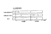
図8は、特許文献1に記載された均等化装置を概略的に示す説明図であり、均等化対象となる単位電池51の正極は抵抗R51、スイッチSW51を介して測定装置52の端子T51に接続され、負極は抵抗R52、スイッチSW52を介して測定装置52の端子T52に接続されている。また、2つの端子T51,T52間には、スイッチSW53と抵抗R53の直列接続回路が設けられている。そして、電圧均等化時には、各スイッチSW51,SW52を共にオンとし、且つ、スイッチSW53をオンすることにより、放電抵抗R53に放電電流を流して単位電池51の電力を消費して、該単位電池51の電圧を低下させる。
FIG. 8 is an explanatory diagram schematically showing the equalization apparatus described in
また、スイッチSW53の診断時には、各スイッチSW51,SW52を共にオンとし、この状態で、スイッチSW53をオフとした場合の端子間電圧、及びスイッチSW53をオンとした場合の端子間電圧を測定装置52で測定し、この測定結果に基づいて、均等化スイッチSW53が正常であるか否かを判定する。即ち、スイッチSW53のオフ時には、測定装置52では、単位電池51の両端電圧が検出され、スイッチSW53のオン時には、抵抗R51〜R53の分圧比に応じた電圧が検出されるので、これらの検出電圧に基づいて、均等化スイッチSW53が正常に作動しているか否かを判定することができる。
At the time of diagnosis of the switch SW53, both the switches SW51 and SW52 are turned on. In this state, the voltage between the terminals when the switch SW53 is turned off and the voltage between the terminals when the switch SW53 is turned on are measured. It is determined whether or not the equalization switch SW53 is normal based on the measurement result. That is, when the switch SW53 is off, the
しかしながら、上述した特許文献1の均等化装置では、均等化スイッチSW53をオンとした状態、及びオフとした場合の2つの状態で電圧を検出する必要があるので、故障診断時に要する工程数が多いという問題がある。また、均等化スイッチSW53が正常に作動しているか否かを診断することができるものの、均等化スイッチSW53を作動させるための駆動装置(図示省略)に異常が発生している場合には、これを検出することができないという欠点がある。このため、均等化スイッチSW53が正常に作動しているにも関わらず、異常であるものと誤検出するという問題が発生することがある。
However, in the equalization apparatus disclosed in
本発明は、このような従来の課題を解決するためになされたものであり、その目的とするところは、組電池を構成する各電池ブロックの電圧を均等化する均等化回路に異常が発生した場合に、迅速、且つ確実にこれを検出することが可能な組電池の電圧均等化装置を提供することにある。 The present invention has been made to solve such a conventional problem, and the object of the present invention is that an abnormality has occurred in the equalization circuit that equalizes the voltages of the battery blocks constituting the assembled battery. It is an object of the present invention to provide an assembled battery voltage equalization apparatus capable of detecting this quickly and reliably.
上記目的を達成するため、本願請求項1に記載の発明は、1以上の単位電池からなる電池ブロックを複数個直列接続して、該直列接続の両端に所望の電圧を発生させる組電池に設けられ、前記各電池ブロック毎の出力電圧を均等化する電圧均等化装置において、前記各電池ブロックの正極、負極間に設けられ、放電抵抗を経由した各電池ブロックの正極、負極間の接続、遮断を切り替える均等化スイッチと、均等化開始指令が与えられた際に、前記各均等化スイッチの接続、遮断を決定する第1の状態信号(例えば「1」)または第2の状態信号(例えば「0」)のビット列からなる均等化制御信号を生成し、該均等化制御信号を、対応する前記均等化スイッチにそれぞれ出力して、該均等化スイッチの接続、遮断を制御する均等化制御手段と、前記各電池ブロックの、前記均等化スイッチと前記放電抵抗との接続点に生じる電圧に基づく第1の状態信号または第2の状態信号のビット列からなる均等化検出信号を取得し、且つ、前記均等化制御信号を取得し、前記均等化検出信号、及び前記均等化制御信号に基づいて、前記各均等化スイッチの作動状態を診断する均等化診断手段と、前記均等化開始指令が与えられた際に前記第1の状態信号または第2の状態信号のうち一方の信号を出力し、均等化終了指令が与えられた際に前記第1の状態信号または第2の状態信号のうち他方の信号を出力するラッチ回路と、を備え、前記均等化診断手段は、前記各均等化スイッチに対応する前記均等化検出信号と前記均等化制御信号とを対比し、且つ、前記ラッチ回路の出力信号であるラッチ信号を考慮して、前記各電池ブロックでの均等化処理が正常に実行されているか否かを判定することを特徴とする。
In order to achieve the above object, the invention described in
請求項2に記載の発明は、前記均等化制御手段は、一の電池ブロックについて、均等化を実行する場合に第1の状態信号、実行しない場合に第2の状態信号となる均等化制御信号を出力し、前記均等化検出信号は、前記一の電池ブロックに対応する均等化スイッチが接続された際に第1の状態信号とされ、遮断された際に第2の状態信号とされ、前記均等化診断手段は、前記一の電池ブロックに対応する均等化スイッチについて、前記均等化検出信号と前記均等化制御信号が一致する場合には、この均等化スイッチの動作は正常であり、前記均等化検出信号と前記均等化制御信号が不一致の場合には、この均等化スイッチの動作は異常であると判定することを特徴とする。 The invention according to claim 2 is characterized in that the equalization control means is an equalization control signal that becomes a first state signal when equalization is performed and a second state signal when equalization is not performed. The equalization detection signal is a first state signal when an equalization switch corresponding to the one battery block is connected, and a second state signal when the equalization switch is cut off. When the equalization detection signal coincides with the equalization control signal for the equalization switch corresponding to the one battery block, the equalization diagnosis means operates normally and the equalization switch When the equalization detection signal and the equalization control signal do not match, it is determined that the operation of the equalization switch is abnormal.
請求項3に記載の発明は、前記ラッチ信号は、前記均等化開始指令が与えられた際に第1の状態信号とされ、前記均等化終了指令が与えられた際に第2の状態信号とされ、前記均等化診断手段は、一の電池ブロックについて、前記ラッチ信号が第1の状態信号のときに、前記均等化検出信号、及び前記均等化制御信号が共に第1の状態信号である場合に、この均等化スイッチの動作は正常であると判定し、前記ラッチ信号が第2の状態信号のときに、前記均等化検出信号、及び前記均等化制御信号の少なくとも一方が第1の状態信号である場合に、この均等化スイッチの動作は異常であると判定することを特徴とする。
According to a third aspect of the present invention, the latch signal is a first state signal when the equalization start command is given, and a second state signal when the equalization end command is given. And the equalization diagnosis means is configured such that the equalization detection signal and the equalization control signal are both the first state signal when the latch signal is the first state signal for one battery block. In addition, when it is determined that the operation of the equalization switch is normal and the latch signal is the second state signal, at least one of the equalization detection signal and the equalization control signal is the first state signal. In this case, the operation of the equalization switch is determined to be abnormal.
本発明に係る電圧均等化装置では、均等化制御信号、及び均等化検出信号に基づいて、各電池ブロックにて均等化処理が正常に実行されているか否かを診断することができるので、多くの工程を必要とせず、且つ高精度に均等化処理の異常を検出することができる。 In the voltage equalization apparatus according to the present invention, it is possible to diagnose whether the equalization process is normally executed in each battery block based on the equalization control signal and the equalization detection signal. It is possible to detect the abnormality in the equalization process with high accuracy without the need for this step.
[第1実施形態の説明]
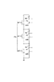
以下、本発明の実施形態を図面に基づいて説明する。図1は、本発明の第1実施形態に係る組電池の電圧均等化装置、及び該電圧均等化装置に接続される組電池の構成を示すブロックである。図1に示すように、組電池23は、例えば電気自動車に設けられる二次電池として用いられ、互いに直列接続された3個の単位電池BT1〜BT3(例えば、リチウムイオン電池)を備えている。なお、本実施形態では、説明を容易にするため3個の単位電池BT1〜BT3を示しているが、単位電池の個数が1個、2個、或いは4個以上であっても良い。
[Description of First Embodiment]
Hereinafter, embodiments of the present invention will be described with reference to the drawings. FIG. 1 is a block diagram showing a configuration of a battery pack voltage equalizing apparatus according to the first embodiment of the present invention and a battery pack connected to the voltage equalizing apparatus. As shown in FIG. 1, the assembled
また、図1に示す電圧均等化装置は、上位システムより与えられる均等化開始指令、或いは均等化終了指令に基づいて、均等化制御を実行するか否かを示す「1」(第1の状態信号)、或いは「0」(第2の状態信号)のラッチ信号を出力するラッチ回路13と、均等化開始指令、及び均等化終了指令に基づいて「1」、「0」のビット列からなる均等化制御信号を出力する均等化制御部15と、ラッチ回路13より出力されるラッチ信号、均等化制御部15より出力される均等化制御信号、及び後述する均等化検出信号に基づいて、電圧の均等化処理が正常に実行されているか否かを診断する均等化診断部14と、を備えている。
Further, the voltage equalization apparatus shown in FIG. 1 indicates “1” (first state) indicating whether or not the equalization control is executed based on the equalization start command or the equalization end command given from the host system. Signal) or a
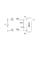
ラッチ回路13は、反転回路NOT4と、アンド回路AND1、及びオア回路OR1を備えており、均等化開始指令が入力された場合には出力信号を「1」(Hレベル)にラッチし、均等化終了指令が入力された場合には出力信号を「0」(Lレベル)にラッチする。そして、該ラッチ回路13より出力される「1」、「0」からなるラッチ信号は、均等化診断部14の端子「C」に供給される。
The
図2は、ラッチ回路13の出力信号の変化を示す説明図であり、均等化開始指令が「0」から「1」切り替わった時点で、ラッチ信号は「0」から「1」に変化し、その後、均等化開始指令が「0」となっても、ラッチ信号の「1」は維持される。そして、均等化終了指令が「0」から「1」に切り替わった時点で、ラッチ信号は「1」から「0」に変化する。その後、均等化終了指令が「0」となっても、ラッチ信号の「0」は維持されるように動作する。
FIG. 2 is an explanatory diagram showing a change in the output signal of the
図1に示す均等化制御部15は、単位電池BT1〜BT3の個数に応じたビット列となる均等化制御信号を出力するものであり、出力電圧が過多であると判定された単位電池(電圧の測定手法については説明を省略)に対応するビットを「1」(第1の状態信号)とし、出力電圧が正常であると判定された単位電池に対応するビットを「0」(第2の状態信号)とするビット列の均等化制御信号を出力する。例えば、電圧測定の結果、単位電池BT2の出力電圧が正常であり、単位電池BT1及びBT3の出力電圧が過多であると判定されている場合には、BT1,BT2,BT3の順に、「1,0,1」のビット列となる均等化制御信号を出力する。
The
この均等化制御信号は、一旦レジスタ17に記憶され、その後、各単位電池BT1〜BT3に設けられる均等化スイッチSW1〜SW3(後述)に出力される。具体的には、均等化スイッチSW1,SW3には、オンを指示する「1」のビット信号が出力され、均等化スイッチSW2には、オフを指示する「0」のビット信号が出力される。また、レジスタ17に記憶された均等化制御信号「1,0,1」は均等化診断部14の端子「B」に供給される。
The equalization control signal is temporarily stored in the
一方、単位電池BT1の正極と負極(グランド)との間には、放電抵抗R1と均等化スイッチSW1の直列接続回路が設けられ、放電抵抗R1と均等化スイッチSW1との接続点P1は、反転回路NOT1を経由してレジスタ16に接続されている。従って、接続点P1の電圧がHレベルである場合には、反転回路NOT1の出力信号はLレベル(これを「0」とする)となり、接続点P1の電圧がLレベルである場合には、反転回路NOT1の出力信号はHレベル(これを「1」とする)となり、これらの信号がレジスタ16に供給される。
On the other hand, a series connection circuit of the discharge resistor R1 and the equalization switch SW1 is provided between the positive electrode and the negative electrode (ground) of the unit battery BT1, and the connection point P1 between the discharge resistor R1 and the equalization switch SW1 is inverted. It is connected to the
また、単位電池BT2の正極と負極(BT1の正極)との間には、放電抵抗R2と均等化スイッチSW2の直列接続回路が設けられ、放電抵抗R2と均等化スイッチSW2との接続点P2は、レベルシフト回路11、及び反転回路NOT2を経由してレジスタ16に接続されている。レベルシフト回路11は、接続点P2に生じる電圧を、単位電池BT2の負極を基準とした電圧に変換する回路である。従って、接続点P2の電圧がHレベルである場合には、反転回路NOT2の出力信号は「0」となり、接続点P2の電圧がLレベルである場合には、反転回路NOT2の出力信号は「1」となる。
Further, a series connection circuit of the discharge resistor R2 and the equalization switch SW2 is provided between the positive electrode and the negative electrode (BT1 positive electrode) of the unit battery BT2, and a connection point P2 between the discharge resistor R2 and the equalization switch SW2 is Are connected to the
更に、単位電池BT3の正極と負極(BT2の正極)との間には、放電抵抗R3と均等化スイッチSW3の直列接続回路が設けられ、放電抵抗R3と均等化スイッチSW3との接続点P3は、レベルシフト回路12、及び反転回路NOT3を経由してレジスタ16に接続されている。レベルシフト回路12は、接続点P3に生じる電圧を、単位電池BT3の負極を基準とした電圧に変換する回路である。従って、接続点P3の電圧がHレベルである場合には、反転回路NOT3の出力信号は「0」となり、接続点P3の電圧がLレベルである場合には、反転回路NOT3の出力信号は「1」となる。
Further, a series connection circuit of a discharge resistor R3 and an equalization switch SW3 is provided between the positive electrode and the negative electrode (positive electrode of BT2) of the unit battery BT3, and a connection point P3 between the discharge resistor R3 and the equalization switch SW3 is Are connected to the
レジスタ16は、各反転回路NOT1〜NOT3より出力される「0」または「1」からなる3個のビット列からなる均等化検出信号を一旦記憶し(この例では、「1,0,1」)、この均等化検出信号を均等化診断部14に出力する。この均等化検出信号は、均等化診断部14の端子「A」に供給される。
The
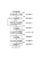
次に、上述した本実施形態に係る電圧均等化装置の動作を、図5に示すフローチャートを参照して説明する。初めに、ラッチ回路13に均等化開始指令が入力されたか否かを判定し(ステップS11)、均等化開始指令が入力されない場合には(ステップS11でNO)、ステップS18に処理を進める。他方、均等化開始指令が入力された場合には(ステップS11でYES)、均等化制御部15は、均等化対象となる単位電池に対応するビットを「1」とするビット列の均等化制御信号を生成し、これをレジスタ17に出力する(ステップS12)。例えば、単位電池BT1,BT3が均等化の対象である場合には、「1,0,1」のビット列となる均等化制御信号を出力する。
Next, the operation of the voltage equalizing apparatus according to this embodiment described above will be described with reference to the flowchart shown in FIG. First, it is determined whether or not an equalization start command is input to the latch circuit 13 (step S11). If an equalization start command is not input (NO in step S11), the process proceeds to step S18. On the other hand, when the equalization start command is input (YES in step S11), the
この均等化制御信号は、均等化診断部14の端子「B」に供給されると共に(ステップS13)、各均等化スイッチSW1〜SW3に供給される。そして、各均等化スイッチSW1〜SW3は、均等化制御信号に応じてオン、オフが切り替えられる(ステップS14)。この例では、均等化スイッチSW1,SW3がオンとされ、均等化スイッチSW2はオフとされる。 The equalization control signal is supplied to the terminal “B” of the equalization diagnosis unit 14 (step S13) and is also supplied to the equalization switches SW1 to SW3. And each equalization switch SW1-SW3 is switched on and off according to the equalization control signal (step S14). In this example, equalization switches SW1 and SW3 are turned on, and equalization switch SW2 is turned off.
その結果、各単位電池BT1,BT3は、それぞれ放電抵抗R1,R3を介して正極と負極が導通するので、放電抵抗R1,R3に放電電流が流れて電力が消費され、各単位電池BT1,BT3の電圧は通常の電圧値まで低下する。即ち、各単位電池BT1〜BT3の均等化処理が実行される。 As a result, each of the unit batteries BT1 and BT3 is electrically connected to the positive electrode and the negative electrode through the discharge resistors R1 and R3, so that a discharge current flows through the discharge resistors R1 and R3 and power is consumed. The voltage drops to the normal voltage value. That is, the equalization process of each unit battery BT1 to BT3 is executed.
次いで、各均等化スイッチSW1〜W3と各放電抵抗R1〜R3の接続点P1〜P3に発生する電圧値に応じた「1」、「0」のビット信号がレジスタ16に供給され、該レジスタ16では、これらの信号を各均等化スイッチSW1〜SW3に応じたビット列の均等化検出信号として、均等化診断部14に出力する。その結果、均等化診断部14の端子「A」に均等化検出信号が供給される(ステップS15)。
Next, bit signals “1” and “0” corresponding to voltage values generated at the connection points P1 to P3 of the equalization switches SW1 to W3 and the discharge resistors R1 to R3 are supplied to the
本実施形態では、均等化スイッチSW1はオンとなるので、接続点P1の電圧はグランド電圧を示す「0」となり、これを反転した「1」がレジスタ16に供給される。また、均等化スイッチSW2はオフとなるので、接続点P2の電圧は単位電池BT2の正極と同一の電圧を示す「1」となり、これを反転した「0」がレジスタ16に供給される。更に、均等化スイッチSW3はオンとなるので、接続点P3の電圧は単位電池BT3の負極と同一の電圧を示す「0」となり、これを反転した「1」がレジスタ16に供給される。
In this embodiment, since the equalization switch SW1 is turned on, the voltage at the connection point P1 becomes “0” indicating the ground voltage, and “1” obtained by inverting this is supplied to the
従って、レジスタ16より出力される均等化検出信号のビット列は「1,0,1」となり、このビット列が均等化診断部14の端子「A」に供給されることになる。
Accordingly, the bit string of the equalization detection signal output from the
そして、均等化診断部14は、端子「A」に供給される均等化検出信号、及び端子「B」に供給される均等化制御信号に基づいて、均等化処理が正常に実行されているか否かを診断する(ステップS16)。
Then, the
一方、ステップS11でNO判定の場合には、電源投入時または診断タイミングであるか否かを判断する(ステップS18)。即ち、均等化診断部14では、均等化の実行時以外にも、電源投入時、及び所定の時間間隔に設定される診断タイミングで均等化が正常に実行されているか否かを判断する。
On the other hand, if NO is determined in step S11, it is determined whether the power is turned on or the diagnosis timing is reached (step S18). That is, the
そして、電源投入時、及び診断タイミングのいずれでもない場合には(ステップS18でNO)、本処理を終了する。また、電源投入時、或いは診断タイミングである場合には(ステップS18でYES)、均等化診断部14は、レジスタ17に記憶されているビット信号を取得する(ステップS19)。更に、レジスタ16に記憶されているビット信号を取得する(ステップS20)。
Then, when it is not at the time of turning on the power or at the diagnosis timing (NO in step S18), this processing is terminated. Further, when the power is turned on or at the diagnosis timing (YES in step S18), the
その後、前述したように均等化診断部14は、ステップS16の処理により、端子「A」に供給される均等化検出信号、及び端子「B」に供給される均等化制御信号に基づいて、均等化処理が正常に実行されているか否かを診断する。
Thereafter, as described above, the
以下、均等化診断部14による診断処理について、図3に示す真理値表を参照して説明する。
Hereinafter, the diagnosis processing by the
図3は、端子「A」に入力される均等化検出信号(これを「入力A」という)、及び端子「B」に入力される均等化制御信号(これを「入力B」という)の状態と、診断結果の関係を示す真理値表である。図示のように、入力A、入力Bが共に「0」、または共に「1」の場合(即ち、双方のビット信号が一致した場合)には、均等化の動作は正常であると判断し、入力A、入力Bのうち一方が「0」、他方が「1」である場合(即ち、双方のビット信号が不一致の場合)には、均等化の動作は異常であると判断する。 FIG. 3 shows the state of the equalization detection signal (this is called “input A”) input to the terminal “A” and the equalization control signal (this is called “input B”) input to the terminal “B”. And a truth table showing the relationship between diagnosis results. As shown in the figure, when both the input A and the input B are “0” or both “1” (that is, when both bit signals match), it is determined that the equalization operation is normal, If one of the inputs A and B is “0” and the other is “1” (that is, if both bit signals do not match), it is determined that the equalization operation is abnormal.
即ち、均等化制御信号が出力されているにも関わらず均等化スイッチがオンとされない場合、或いは均等化制御信号が出力されていないにも関わらず、均等化スイッチがオンとされた場合に、均等化の動作は異常であると判断する。 That is, when the equalization switch is not turned on even though the equalization control signal is output, or when the equalization switch is turned on although the equalization control signal is not output, It is determined that the equalization operation is abnormal.
そして、均等化制御部14は、この診断結果に応じた出力信号を後段に設けられる警報装置(図示省略)等に出力し(ステップS17)、均等化の動作に異常が発生していることを操作者に報知する。
Then, the
このようにして、本発明の第1実施形態に係る組電池の電圧均等化装置では、均等化制御部15より出力される各単位電池BT1〜BT3の均等化制御信号と、各単位電池BT1〜BT3より出力される均等化検出信号に基づいて、均等化の動作が正常であるか否かを診断している。即ち、均等化診断部14の入力A、入力Bのビット信号の一致、不一致を検出することにより、均等化の動作が正常であるか否かを診断している。
In this way, in the battery pack voltage equalization apparatus according to the first embodiment of the present invention, the equalization control signal of each unit cell BT1 to BT3 output from the
従って、均等化の動作指示を受けているにも関わらず均等化が実施されないことや、均等化の動作指示を受けていないにも関わらず均等化が実施される等の異常が発生した場合に、これを即時に認識して操作者に通知することができる。 Therefore, when an abnormality such as the fact that the equalization is not performed even though the equalization operation instruction is received, or the equalization is performed even though the equalization operation instruction is not received occurs. This can be immediately recognized and notified to the operator.
その結果、従来のように、均等化スイッチをオンとした場合とオフとした場合の電圧値の相違を比較する等の、面倒な操作を必要とせずに、均等化制御部15から各均等化スイッチSW1〜SW3に至るまでの回路が正常に作動しているか否かを診断することができる。
As a result, each
また、第1実施形態では、一つの単位電池毎にそれぞれ均等化スイッチを設け、各単位電池の出力電圧が過多である場合に、均等化スイッチをオンとして個々の単位電池の出力電圧を均等化するので、組電池23を構成するそれぞれの単位電池の出力電圧を一定に保持することができる。
In the first embodiment, an equalization switch is provided for each unit cell, and when the output voltage of each unit battery is excessive, the equalization switch is turned on to equalize the output voltage of each unit cell. Therefore, the output voltage of each unit battery constituting the assembled
[第2実施形態の説明]
次に、本発明の第2実施形態について説明する。第2実施形態に係る組電池の電圧均等化装置は、図1に示した回路と同一の構成であり、均等化診断部14による診断処理の手順のみが相違する。即ち、第1実施形態では、均等化診断部14に供給される均等化検出信号、及び均等化制御信号に基づいて、均等化の動作が正常であるか否かを診断する例について示したが、第2実施形態では、これに加えて端子「C」に供給されるラッチ信号を含めて均等化処理が正常に実行されているか否かの診断を行う。以下、第2実施形態に係る電圧均等化装置の処理動作について、図4に示す真理値表、及び図6に示すフローチャートを参照して説明する。
[Description of Second Embodiment]
Next, a second embodiment of the present invention will be described. The assembled battery voltage equalization apparatus according to the second embodiment has the same configuration as the circuit shown in FIG. 1, and only the procedure of the diagnosis process by the
図4は、均等化診断部14に供給される入力A、入力B、及び入力C(ラッチ信号)の状態と、診断結果の関係を示す真理値表である。図示のように、この真理値表では入力A〜入力Cの各状態に基づいて、均等化装置に故障が発生しているか否かを決めている。即ち、入力Cが「0」のときには、入力A、B、Cの順に「0,0,0」の場合には正常、「0,1,0」の場合には複合的な故障、「1,0,0」の場合には均等化スイッチのショート故障、「1,1,0」の場合には複合的な故障であると判断する。
FIG. 4 is a truth table showing the relationship between the status of the input A, input B, and input C (latch signal) supplied to the
また、入力Cが「1」のときには、入力Aのビット信号と入力Bのビット信号が一致した場合には均等化の動作は正常であると判断し、不一致の場合には均等化装置は故障であると判断する。この判断は、入力A、B、Cの順に「0,1,1」の場合には均等化スイッチのオープン故障、「1,0,1」の場合には複合的な故障、「1,1,1」の場合には正常であると判断する。但し、「0,0,1」の場合には、ビットを限定して判断することになる。つまり、ラッチ回路13の出力信号である入力Cが「1」であっても、均等化対象とされていない単位電池BT2に対しては入力A、入力Bが共に「0」のときに正常となるので、ビットに応じて、正常、異常を判断することになる。
When the input C is “1”, if the bit signal of the input A and the bit signal of the input B match, it is determined that the equalization operation is normal. It is judged that. This determination is made in the order of inputs A, B, and C in the case of “0, 1, 1”, an open failure of the equalization switch, and in the case of “1, 0, 1”, a complex failure, “1, 1 , 1 ”, it is determined to be normal. However, in the case of “0, 0, 1”, the determination is made by limiting the bits. That is, even if the input C, which is the output signal of the
次に、図6に示すフローチャートを参照して、第2実施形態に係る電圧均等化装置の動作について説明する。 Next, the operation of the voltage equalizing apparatus according to the second embodiment will be described with reference to the flowchart shown in FIG.
初めに、均等化診断部14は、ラッチ回路13より出力されるラッチ信号(出力ビット)を取得する(ステップS31)。即ち、上位装置から均等化開始指令が与えられた場合には、ラッチ回路13より「1」のビット信号が出力されて均等化診断部14の入力Cに供給され、上位装置から均等化終了指令が与えられた場合には、ラッチ回路13より「0」のビット信号が出力されて均等化診断部14の入力Cに供給される。
First, the
次いで、均等化診断部14は、ラッチ回路13の出力ビットが「1」であるか否かを判断し(ステップS32)、「1」である場合にはステップS33に処理を進め、「0」である場合にはステップS34に処理を進める。
Next, the
ステップS33において、均等化制御部15は、均等化対象とする単位電池に対応するビットを「1」とするビット信号からなる均等化制御信号を生成して出力する。例えば、単位電池BT1,BT3を均等化し、単位電池BT2を均等化しない場合には、この均等化制御信号は「1,0,1」となる。
In step S <b> 33, the
ステップS34において、均等化診断部14は、均等化制御部15より出力されるビット信号(均等化制御信号)を取得する。即ち、均等化制御部15より出力される均等化制御信号は、均等化診断部14の端子「B」に供給され、均等化診断部14はこれを取得する。また、ラッチ回路13出力ビットが「0」である場合には、均等化制御部15は「0,0,0」を出力するので、均等化診断部14の端子「B」には「0,0,0」の均等化制御信号が供給される。
In step S <b> 34, the
更に、均等化制御信号は、各均等化スイッチSW1〜SW3に供給される。そして、各均等化スイッチSW1〜SW3は、均等化制御信号に応じて、オン、オフが切り替えられる(ステップS35)。この例では、均等化スイッチSW1,SW3がオンとされ、均等化スイッチSW2はオフとされる。 Further, the equalization control signal is supplied to the equalization switches SW1 to SW3. And each equalization switch SW1-SW3 is switched on and off according to the equalization control signal (step S35). In this example, equalization switches SW1 and SW3 are turned on, and equalization switch SW2 is turned off.
その結果、各単位電池BT1,BT3は、それぞれ放電抵抗R1,R3を介して正極と負極が導通するので、放電抵抗R1,R3に放電電流が流れて電力が消費され、各単位電池BT1,BT3の電圧は通常の電圧値まで低下する。即ち、各単位電池BT1〜BT3の均等化処理が実行される。 As a result, each of the unit batteries BT1 and BT3 is electrically connected to the positive electrode and the negative electrode through the discharge resistors R1 and R3, so that a discharge current flows through the discharge resistors R1 and R3 and power is consumed. The voltage drops to the normal voltage value. That is, the equalization process of each unit battery BT1 to BT3 is executed.
次いで、各均等化スイッチSW1〜W3と各放電抵抗R1〜R3の接続点P1〜P3に発生する電圧値に応じた「1」、「0」のビット信号がレジスタ16に供給され、該レジスタ16では、これらの信号を各均等化スイッチSW1〜SW3に応じたビット列の均等化検出信号として、均等化診断部14に出力する。その結果、均等化診断部14の端子「A」に均等化検出信号が供給される(ステップS36)。
Next, bit signals “1” and “0” corresponding to voltage values generated at the connection points P1 to P3 of the equalization switches SW1 to W3 and the discharge resistors R1 to R3 are supplied to the
そして、図4に示した真理値表、及び均等化診断部14の各入力端子「A」「B」「C」より取得される各ビット信号に基づいて、前述した第1実施形態と同様に、均等化の動作が正常であるか否かを診断する(ステップS37)。
Then, based on the truth table shown in FIG. 4 and each bit signal acquired from each of the input terminals “A”, “B”, and “C” of the
その後、この診断結果を、後段に設けられる警報装置(図示省略)等に出力して(ステップS38)、均等化の動作に異常が発生していることを操作者に報知する。 Thereafter, the diagnosis result is output to an alarm device (not shown) or the like provided in the subsequent stage (step S38) to notify the operator that an abnormality has occurred in the equalization operation.
このようにして、本発明の第2実施形態に係る電圧均等化装置では、均等化制御部15より出力される各単位電池BT1〜BT3の均等化制御信号と、各単位電池BT1〜BT3より出力される均等化検出信号、及びラッチ回路13より出力されるラッチ信号に基づいて、均等化の動作が正常に行われているか否かを診断している。即ち、ラッチ信号が「0」或いは「1」の場合において、均等化診断部14の入力A、入力Bのビット信号の一致、不一致を検出することにより、均等化の動作が正常であるか否かを診断している。
Thus, in the voltage equalization apparatus according to the second embodiment of the present invention, the equalization control signal of each unit battery BT1 to BT3 output from the
従って、前述した第1実施形態と同様に、均等化の動作指示を受けているにも関わらず均等化が実施されないことや、均等化の動作指示を受けていないにも関わらず均等化が実施される等の異常が発生した場合に、これを即時に認識して作業者に通知することができる。 Accordingly, as in the first embodiment described above, equalization is not performed even when an equalization operation instruction is received, or equalization is performed even when an equalization operation instruction is not received. When an abnormality such as being generated occurs, this can be immediately recognized and notified to the operator.
その結果、従来のように、均等化スイッチをオンとした場合とオフとした場合の電圧値の相違を検出する等の、面倒な操作を必要とせずに、均等化制御部15から各均等化スイッチSW1〜SW3に至るまでの回路が正常に作動しているか否かを診断することができる。
As a result, each
ここで、前述した第1、第2実施形態では、組電池23に設けられた3個の単位電池BT1〜BT3を均等化する例について説明したが、複数の直列接続された単位電池毎に出力電圧を均等化するように構成しても良い。即ち、図7に示すように、複数の組電池からなる電池ブロックBT11,BT12,BT13を直列接続して組電池23aを構成し、各電池ブロックBT11〜BT13毎にそれぞれ電圧を測定し、電圧が高い場合に均等化スイッチSW1〜SW3をオンとして各電池ブロックBT11〜BT13毎の出力電圧を均等化する構成としても可能である。この場合、各電池ブロックBT11〜BT13に設けられる単位電池の個数は同一であっても良いし、同一で無くても良い。
Here, in the first and second embodiments described above, the example in which the three unit batteries BT1 to BT3 provided in the assembled
以上、本発明の組電池の電圧均等化装置を図示の実施形態に基づいて説明したが、本発明はこれに限定されるものではなく、各部の構成は、同様の機能を有する任意の構成のものに置き換えることができる。 As mentioned above, although the voltage equalization apparatus of the assembled battery of this invention was demonstrated based on embodiment of illustration, this invention is not limited to this, The structure of each part is arbitrary structures which have the same function. Can be replaced with something.
例えば、上述した各実施形態では、図1に示したように、各接続点P1〜P3の後段側に反転回路NOT1〜NOT3を設ける例について説明したが、これらの反転回路NOT1〜NOT3を割愛し、均等化診断部14内における判定処理で「1」、「0」の論理を反転させることで、同様の結果を得ることも可能である。具体的には、図3,図4に示した真理値表の「入力A」の信号の「1」、「0」を反転させて診断結果を取得すれば良い。このように、上述の各実施形態において、「1」、「0」のビット信号を反転させ、これに合わせて論理演算を反転させることで、実質的に同一の処理を行うことが可能である。
For example, in each of the above-described embodiments, as illustrated in FIG. 1, the example in which the inverting circuits NOT1 to NOT3 are provided on the subsequent stage side of the connection points P1 to P3 has been described, but the inverting circuits NOT1 to NOT3 are omitted. Similar results can be obtained by inverting the logic of “1” and “0” in the determination process in the
また、本実施形態では、電気自動車の二次電池として用いられる組電池を均等化する例について説明したが、車両以外に搭載される組電池についても適用することができる。 Moreover, although this embodiment demonstrated the example which equalizes the assembled battery used as a secondary battery of an electric vehicle, it is applicable also to the assembled battery mounted in addition to a vehicle.
本発明は、組電池に設けられる各単位電池の出力電圧を均等化する回路に異常が発生した場合に、いち早くこれを検出する上で極めて有用である。 The present invention is extremely useful for quickly detecting an abnormality in a circuit that equalizes the output voltage of each unit battery provided in an assembled battery.
11,12 レベルシフト回路
13 ラッチ回路
14 均等化診断部(均等化診断手段)
15 均等化制御部(均等化制御手段)
16,17 レジスタ
21,22 レベルシフト回路
23,23a 組電池
BT1〜BT3 単位電池
BT11〜BT13 電池ブロック
R1〜R3 放電抵抗
SW1〜SW3 均等化スイッチ
NOT1〜NOT4 反転回路
BT1〜BT3 単位電池
OR1 オア回路
AND1 アンド回路
11, 12
15 Equalization control unit (equalization control means)
16, 17
AND1 AND circuit
Claims (3)
前記各電池ブロックの正極、負極間に設けられ、放電抵抗を経由した各電池ブロックの正極、負極間の接続、遮断を切り替える均等化スイッチと、
均等化開始指令が与えられた際に、前記各均等化スイッチの接続、遮断を決定する第1の状態信号または第2の状態信号のビット列からなる均等化制御信号を生成し、該均等化制御信号を、対応する前記均等化スイッチにそれぞれ出力して、該均等化スイッチの接続、遮断を制御する均等化制御手段と、
前記各電池ブロックの、前記均等化スイッチと前記放電抵抗との接続点に生じる電圧に基づく第1の状態信号または第2の状態信号のビット列からなる均等化検出信号を取得し、且つ、前記均等化制御信号を取得し、前記均等化検出信号、及び前記均等化制御信号に基づいて、前記各均等化スイッチの作動状態を診断する均等化診断手段と、
前記均等化開始指令が与えられた際に前記第1の状態信号または第2の状態信号のうち一方の信号を出力し、均等化終了指令が与えられた際に前記第1の状態信号または第2の状態信号のうち他方の信号を出力するラッチ回路と、を備え、
前記均等化診断手段は、前記各均等化スイッチに対応する前記均等化検出信号と前記均等化制御信号とを対比し、且つ、前記ラッチ回路の出力信号であるラッチ信号を考慮して、前記各電池ブロックでの均等化処理が正常に実行されているか否かを判定すること
を特徴とする組電池の電圧均等化装置。 Voltage equalization that is provided in an assembled battery in which a plurality of battery blocks including one or more unit cells are connected in series and generates a desired voltage at both ends of the series connection, and equalizes the output voltage of each battery block. In the device
An equalization switch that is provided between the positive electrode and the negative electrode of each battery block, and switches between connection and disconnection between the positive electrode and the negative electrode of each battery block via a discharge resistor,
When an equalization start command is given, an equalization control signal composed of a bit string of the first state signal or the second state signal that determines connection / cutoff of each equalization switch is generated, and the equalization control An equalization control means for outputting a signal to each of the corresponding equalization switches to control connection and disconnection of the equalization switches;
An equalization detection signal consisting of a bit string of a first state signal or a second state signal based on a voltage generated at a connection point between the equalization switch and the discharge resistor of each battery block is acquired, and the equalization An equalization diagnosis means for obtaining an equalization control signal and diagnosing an operation state of each equalization switch based on the equalization detection signal and the equalization control signal ;
When the equalization start command is given, one of the first status signal and the second status signal is output, and when the equalization end command is given, the first status signal or the second status signal is output. A latch circuit that outputs the other of the two status signals ,
The equalization diagnosis means compares the equalization detection signal corresponding to each equalization switch with the equalization control signal, and considers each latch signal that is an output signal of the latch circuit. A voltage equalizing apparatus for an assembled battery, wherein it is determined whether or not the equalization processing in the battery block is normally executed.
前記均等化検出信号は、前記一の電池ブロックに対応する均等化スイッチが接続された際に第1の状態信号とされ、遮断された際に第2の状態信号とされ、
前記均等化診断手段は、前記一の電池ブロックに対応する均等化スイッチについて、前記均等化検出信号と前記均等化制御信号が一致する場合には、この均等化スイッチの動作は正常であり、前記均等化検出信号と前記均等化制御信号が不一致の場合には、この均等化スイッチの動作は異常であると判定することを特徴とする請求項1に記載の組電池の電圧均等化装置。 The equalization control means outputs, with respect to one battery block, an equalization control signal that becomes a first state signal when equalization is executed, and becomes a second state signal when it is not executed,
The equalization detection signal is a first state signal when an equalization switch corresponding to the one battery block is connected, and a second state signal when the equalization switch is cut off.
When the equalization detection signal and the equalization control signal coincide with each other for the equalization switch corresponding to the one battery block, the equalization diagnosis means operates normally. 2. The assembled battery voltage equalization apparatus according to claim 1, wherein when the equalization detection signal and the equalization control signal do not match, the operation of the equalization switch is determined to be abnormal .
前記均等化診断手段は、一の電池ブロックについて、
前記ラッチ信号が第1の状態信号のときに、前記均等化検出信号、及び前記均等化制御信号が共に第1の状態信号である場合に、この均等化スイッチの動作は正常であると判定し、
前記ラッチ信号が第2の状態信号のときに、前記均等化検出信号、及び前記均等化制御信号の少なくとも一方が第1の状態信号である場合に、この均等化スイッチの動作は異常であると判定することを特徴とする請求項2に記載の組電池の電圧均等化装置。 The latch signal is a first state signal when the equalization start command is given, and a second state signal when the equalization end command is given,
The equalization diagnosis means is for one battery block.
When the latch signal is the first state signal and the equalization detection signal and the equalization control signal are both the first state signal, it is determined that the operation of the equalization switch is normal. ,
The operation of the equalization switch is abnormal when at least one of the equalization detection signal and the equalization control signal is the first state signal when the latch signal is the second state signal. battery pack voltage equalizer of claim 2 you and judging.
Priority Applications (5)
| Application Number | Priority Date | Filing Date | Title |
|---|---|---|---|
| JP2010159441A JP5571485B2 (en) | 2010-07-14 | 2010-07-14 | Voltage equalization device for battery pack |
| PCT/JP2011/065888 WO2012008448A1 (en) | 2010-07-14 | 2011-07-12 | Assembled-battery voltage equalization apparatus |
| EP11806778.4A EP2595275B1 (en) | 2010-07-14 | 2011-07-12 | Assembled-battery voltage equalization apparatus |
| CN201180034720.4A CN103119827B (en) | 2010-07-14 | 2011-07-12 | Assembled-battery voltage equalization apparatus |
| US13/809,714 US20130162213A1 (en) | 2010-07-14 | 2011-07-12 | Voltage equalizer for battery pack |
Applications Claiming Priority (1)
| Application Number | Priority Date | Filing Date | Title |
|---|---|---|---|
| JP2010159441A JP5571485B2 (en) | 2010-07-14 | 2010-07-14 | Voltage equalization device for battery pack |
Publications (2)
| Publication Number | Publication Date |
|---|---|
| JP2012023848A JP2012023848A (en) | 2012-02-02 |
| JP5571485B2 true JP5571485B2 (en) | 2014-08-13 |
Family
ID=45469445
Family Applications (1)
| Application Number | Title | Priority Date | Filing Date |
|---|---|---|---|
| JP2010159441A Active JP5571485B2 (en) | 2010-07-14 | 2010-07-14 | Voltage equalization device for battery pack |
Country Status (5)
| Country | Link |
|---|---|
| US (1) | US20130162213A1 (en) |
| EP (1) | EP2595275B1 (en) |
| JP (1) | JP5571485B2 (en) |
| CN (1) | CN103119827B (en) |
| WO (1) | WO2012008448A1 (en) |
Families Citing this family (18)
| Publication number | Priority date | Publication date | Assignee | Title |
|---|---|---|---|---|
| CN102593909A (en) * | 2012-03-02 | 2012-07-18 | 宁德新能源科技有限公司 | Reliability detecting system for battery balancing circuit |
| JP5932569B2 (en) * | 2012-08-24 | 2016-06-08 | ルネサスエレクトロニクス株式会社 | Semiconductor device and battery voltage monitoring device |
| JP6200139B2 (en) * | 2012-09-21 | 2017-09-20 | 矢崎総業株式会社 | Equalization equipment |
| JP5920291B2 (en) * | 2013-08-02 | 2016-05-18 | 株式会社デンソー | Battery pack equalization device |
| CN106160034B (en) * | 2015-03-27 | 2019-06-18 | 海马汽车有限公司 | A kind of battery balanced control device and method |
| CN104901380A (en) * | 2015-06-16 | 2015-09-09 | 北京亿利智慧能源科技有限公司 | Battery pack equalizing control method of multistage equalizing unit |
| CN104967182A (en) * | 2015-07-20 | 2015-10-07 | 苏州衡久电池科技有限公司 | Fast balanced-type protection management method for two-wheeler lithium battery |
| DE102016202761A1 (en) | 2016-02-23 | 2017-08-24 | Continental Automotive Gmbh | Battery system with a voltage compensation circuit, method for detecting a fault condition of the voltage compensation circuit and the cell voltage measurement |
| JP6565746B2 (en) | 2016-03-11 | 2019-08-28 | 株式会社デンソー | Voltage detector |
| CN105633491B (en) * | 2016-03-22 | 2018-02-27 | 深圳市清友能源技术有限公司 | A kind of passive equalizing circuit of battery management system |
| JP6539618B2 (en) * | 2016-07-21 | 2019-07-03 | 矢崎総業株式会社 | Battery monitoring system |
| CN106786944B (en) | 2016-12-31 | 2020-12-18 | 华为技术有限公司 | Sampling circuit, equalization circuit and system of single batteries of series battery pack |
| JP2018117438A (en) * | 2017-01-17 | 2018-07-26 | 太陽誘電株式会社 | Power source module with lithium ion capacitor |
| KR102150147B1 (en) * | 2017-05-24 | 2020-09-01 | 주식회사 엘지화학 | Apparatus and method for balancing battery module |
| US11398647B2 (en) * | 2017-08-01 | 2022-07-26 | Lg Energy Solution, Ltd. | Battery management system |
| JP7226249B2 (en) * | 2019-11-01 | 2023-02-21 | トヨタ自動車株式会社 | BATTERY CONTROL DEVICE AND ABNORMALITY DETECTION METHOD |
| CN113054706A (en) * | 2021-03-18 | 2021-06-29 | 中国第一汽车股份有限公司 | Balance monitoring control system and method for power battery |
| CN116559634B (en) * | 2023-07-11 | 2023-09-12 | 杭州华塑科技股份有限公司 | Circuit fault detection method and device, storage medium and electronic equipment |
Family Cites Families (9)
| Publication number | Priority date | Publication date | Assignee | Title |
|---|---|---|---|---|
| US5965996A (en) * | 1997-12-11 | 1999-10-12 | Vectrix Corporation | Electrical scooter having an equalization circuit for charging multiple batteries |
| JP4605952B2 (en) * | 2001-08-29 | 2011-01-05 | 株式会社日立製作所 | Power storage device and control method thereof |
| JP4092580B2 (en) * | 2004-04-30 | 2008-05-28 | 新神戸電機株式会社 | Multi-series battery control system |
| CN101199094B (en) * | 2006-04-11 | 2011-01-05 | 三菱电机株式会社 | Electric power storage system |
| JP5076812B2 (en) * | 2006-12-18 | 2012-11-21 | 日産自動車株式会社 | Abnormality diagnosis device |
| JP5127383B2 (en) * | 2007-09-28 | 2013-01-23 | 株式会社日立製作所 | Battery integrated circuit and vehicle power supply system using the battery integrated circuit |
| JP5224095B2 (en) * | 2007-12-27 | 2013-07-03 | 株式会社Gsユアサ | Battery management device for battery pack |
| KR101414494B1 (en) * | 2008-03-17 | 2014-07-04 | 삼성전자주식회사 | Memory device and memory data read method |
| JP5486780B2 (en) * | 2008-07-01 | 2014-05-07 | 株式会社日立製作所 | Battery system |
-
2010
- 2010-07-14 JP JP2010159441A patent/JP5571485B2/en active Active
-
2011
- 2011-07-12 WO PCT/JP2011/065888 patent/WO2012008448A1/en active Application Filing
- 2011-07-12 EP EP11806778.4A patent/EP2595275B1/en active Active
- 2011-07-12 US US13/809,714 patent/US20130162213A1/en not_active Abandoned
- 2011-07-12 CN CN201180034720.4A patent/CN103119827B/en active Active
Also Published As
| Publication number | Publication date |
|---|---|
| EP2595275A4 (en) | 2014-03-26 |
| US20130162213A1 (en) | 2013-06-27 |
| EP2595275A1 (en) | 2013-05-22 |
| EP2595275B1 (en) | 2016-05-11 |
| JP2012023848A (en) | 2012-02-02 |
| WO2012008448A1 (en) | 2012-01-19 |
| CN103119827B (en) | 2015-07-08 |
| CN103119827A (en) | 2013-05-22 |
Similar Documents
| Publication | Publication Date | Title |
|---|---|---|
| JP5571485B2 (en) | Voltage equalization device for battery pack | |
| JP5169491B2 (en) | Battery pack monitoring device and battery breakage detection method | |
| JP5076812B2 (en) | Abnormality diagnosis device | |
| JP5224095B2 (en) | Battery management device for battery pack | |
| JP4466628B2 (en) | Voltage detector | |
| JP5110154B2 (en) | Voltage detection device and voltage detection system | |
| JP5326973B2 (en) | Battery monitoring device | |
| US20110121837A1 (en) | Battery pack and method of sensing voltage of battery pack | |
| JP2010091520A (en) | Battery module abnormality detection circuit, and detection method therefor | |
| CN102903983A (en) | Battery cell monitoring circuit, battery cell module, automobile with battery cell module | |
| JP5900431B2 (en) | Battery monitoring device and battery unit | |
| JP2011078165A (en) | Voltage monitoring apparatus | |
| JP2010271267A (en) | Battery monitoring device | |
| JP2013242324A (en) | Battery monitoring device | |
| CN110879350A (en) | Detection method of battery equalization circuit and battery management system | |
| JP2012021868A (en) | Voltage detector for battery pack | |
| JP2011038876A (en) | Voltage measuring instrument for a plurality of battery packs | |
| JP2008064520A (en) | Voltage measuring instrument | |
| JP2018107920A (en) | Controller of battery module | |
| JP2015097461A (en) | Battery pack voltage detector | |
| JP6236775B2 (en) | Detection device | |
| JP5602114B2 (en) | Battery management device, battery management system | |
| KR20220049950A (en) | Relay diagnosis apparatus, relay diagnosis method, and electric vehicle | |
| JP2015102336A (en) | Battery monitoring device | |
| CN111371139A (en) | State diagnosis circuit and method for equalization circuit |
Legal Events
| Date | Code | Title | Description |
|---|---|---|---|
| A621 | Written request for application examination |
Free format text: JAPANESE INTERMEDIATE CODE: A621 Effective date: 20130619 |
|
| A131 | Notification of reasons for refusal |
Free format text: JAPANESE INTERMEDIATE CODE: A131 Effective date: 20140415 |
|
| A521 | Request for written amendment filed |
Free format text: JAPANESE INTERMEDIATE CODE: A523 Effective date: 20140529 |
|
| TRDD | Decision of grant or rejection written | ||
| A01 | Written decision to grant a patent or to grant a registration (utility model) |
Free format text: JAPANESE INTERMEDIATE CODE: A01 Effective date: 20140617 |
|
| A61 | First payment of annual fees (during grant procedure) |
Free format text: JAPANESE INTERMEDIATE CODE: A61 Effective date: 20140626 |
|
| R150 | Certificate of patent or registration of utility model |
Ref document number: 5571485 Country of ref document: JP Free format text: JAPANESE INTERMEDIATE CODE: R150 |
|
| R250 | Receipt of annual fees |
Free format text: JAPANESE INTERMEDIATE CODE: R250 |
|
| R250 | Receipt of annual fees |
Free format text: JAPANESE INTERMEDIATE CODE: R250 |
|
| R250 | Receipt of annual fees |
Free format text: JAPANESE INTERMEDIATE CODE: R250 |
|
| R250 | Receipt of annual fees |
Free format text: JAPANESE INTERMEDIATE CODE: R250 |
|
| R250 | Receipt of annual fees |
Free format text: JAPANESE INTERMEDIATE CODE: R250 |
|
| R250 | Receipt of annual fees |
Free format text: JAPANESE INTERMEDIATE CODE: R250 |
|
| S531 | Written request for registration of change of domicile |
Free format text: JAPANESE INTERMEDIATE CODE: R313531 |
|
| R350 | Written notification of registration of transfer |
Free format text: JAPANESE INTERMEDIATE CODE: R350 |
|
| R250 | Receipt of annual fees |
Free format text: JAPANESE INTERMEDIATE CODE: R250 |
|
| R250 | Receipt of annual fees |
Free format text: JAPANESE INTERMEDIATE CODE: R250 |