JP5551663B2 - Direct RF modulation transmitter - Google Patents
Direct RF modulation transmitter Download PDFInfo
- Publication number
- JP5551663B2 JP5551663B2 JP2011187410A JP2011187410A JP5551663B2 JP 5551663 B2 JP5551663 B2 JP 5551663B2 JP 2011187410 A JP2011187410 A JP 2011187410A JP 2011187410 A JP2011187410 A JP 2011187410A JP 5551663 B2 JP5551663 B2 JP 5551663B2
- Authority
- JP
- Japan
- Prior art keywords
- signal
- transistor
- voltage
- gate
- data
- Prior art date
- Legal status (The legal status is an assumption and is not a legal conclusion. Google has not performed a legal analysis and makes no representation as to the accuracy of the status listed.)
- Expired - Fee Related
Links
- 238000005096 rolling process Methods 0.000 claims 1
- 230000005540 biological transmission Effects 0.000 description 17
- 238000010586 diagram Methods 0.000 description 14
- 238000006243 chemical reaction Methods 0.000 description 11
- 230000008859 change Effects 0.000 description 8
- 238000000034 method Methods 0.000 description 6
- 230000008569 process Effects 0.000 description 6
- 230000000694 effects Effects 0.000 description 5
- 238000005070 sampling Methods 0.000 description 3
- 230000007704 transition Effects 0.000 description 3
- 238000004891 communication Methods 0.000 description 2
- 239000004065 semiconductor Substances 0.000 description 2
- 230000003321 amplification Effects 0.000 description 1
- 230000008901 benefit Effects 0.000 description 1
- 230000000052 comparative effect Effects 0.000 description 1
- 230000008878 coupling Effects 0.000 description 1
- 238000010168 coupling process Methods 0.000 description 1
- 238000005859 coupling reaction Methods 0.000 description 1
- 230000007423 decrease Effects 0.000 description 1
- 229910044991 metal oxide Inorganic materials 0.000 description 1
- 150000004706 metal oxides Chemical class 0.000 description 1
- 238000003199 nucleic acid amplification method Methods 0.000 description 1
- 230000009467 reduction Effects 0.000 description 1
- 238000000926 separation method Methods 0.000 description 1
Images


Landscapes
- Transmitters (AREA)
Description
本発明は、直接RF変調送信器に関する。 The present invention relates to a direct RF modulation transmitter.
現在、複数の無線通信規格や複数の周波数のバンドに対応することができる携帯型の通信端末装置(以下、本明細書では携帯端末と記す)がある。複数の規格に対応することをマルチモード対応といい、複数の周波数のバンドに対応することをマルチバンド対応という。
このようなマルチモードマルチバンド対応端末の送信に係る構成として、デジタルベースバンド信号をアナログ信号に変換(デジタル/アナログ変換)する際に、同時にRF送信キャリア周波数への周波数変換も行い、デジタル信号から直接RF周波数に変調する送信器が近年知られている。このような送信器は、例えば、特許文献1に記載されている。
Currently, there is a portable communication terminal device (hereinafter referred to as a portable terminal in the present specification) that can support a plurality of wireless communication standards and a plurality of frequency bands. Supporting a plurality of standards is called multi-mode support, and supporting a plurality of frequency bands is called multi-band support.
As a configuration related to the transmission of such a multi-mode multi-band compatible terminal, when converting a digital baseband signal into an analog signal (digital / analog conversion), frequency conversion to an RF transmission carrier frequency is also performed at the same time. Transmitters that directly modulate to RF frequencies are known in recent years. Such a transmitter is described in
特許文献1に記載された送信器では、広く知られた電流制御型デジタル/アナログ変換回路におけるトランジスタの縦積み回路の一部に、ギルバートセルミキサに類似した構成のRF周波数変換回路を組み込んでいる。このような構成によれば、デジタル/アナログ変換器とRF周波数変換器、あるいはRF変調器を独立した回路とし、デジタル/アナログ変換とRF周波数変換とを複合化して同時に行うことができる。
In the transmitter described in
特許文献1に記載された送信器は、デジタル/RF変換器(Digital to RF converter)、直接RF変換器(Direct RF converter)、あるいは、それらによって構成される直接RF変調送信器(Direct RF Modulation Transmitter)等と呼ばれることがある。このような構成を送信器に用いると、従来型の分離動作する送信器において必要とされる、デジタル/アナログ変換器とRF周波数変換器との間のアナログベースバンドフィルタ回路を省略できる等の利点がある。
The transmitter described in
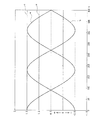
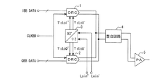
図11は、上記した直接RF変調送信器の構成を例示した図である。図11に示した直接RF変調送信器は、2つのデジタル/RF変換器(図中にDRCと記す)1、2、2分周器3、整合回路4、パワーアンプ(図中にPAと記す)5とから構成される。
2分周器3には、周波数掛算用のRF信号(以下、送信ローカルRF信号と記す)Loin+、送信ローカルRF信号Loin+の位相が反転された送信ローカルRF信号Loin−が外部から供給されている。2分周器3は、送信ローカルRF信号Loin+、Loin−を入力し、90度位相の異なる二対の差動ローカル信号TxLoI+、TxLoI−、TxLoQ+、TxLoQ−を生成し、デジタル/RF変換器1、2に各々出力する。
FIG. 11 is a diagram illustrating the configuration of the direct RF modulation transmitter described above. The direct RF modulation transmitter shown in FIG. 11 includes two digital / RF converters (denoted as DRC in the figure) 1, 2, a frequency divider 3, a matching circuit 4, and a power amplifier (denoted as PA in the figure). ) 5.
The frequency divider 3 is externally supplied with an RF signal for frequency multiplication (hereinafter referred to as a transmission local RF signal) Loin + and a transmission local RF signal Loin- in which the phase of the transmission local RF signal Loin + is inverted. . The frequency divider 3 receives the transmission local RF signals Loin + and Loin−, generates two pairs of differential local signals TxLoI +, TxLoI−, TxLoQ +, and TxLoQ− that are 90 degrees out of phase, 2 and 2 respectively.
図11に示した例では、2分周器3によって0度と90度との差動ローカル信号を生成するため、送信ローカルRF信号Loin+、Loin−の周波数は目的とする送信キャリア波の周波数の2倍になる。差動ローカル信号TxLoI+、TxLoI−、TxLoQ+、TxLoQ−の周波数は送信キャリア波の周波数となる。差動ローカル信号TxLoI+、TxLoI−と、TxLoQ+、TxLoQ−との間には、90度の位相差がある。 In the example shown in FIG. 11, since the differential local signal of 0 degrees and 90 degrees is generated by the frequency divider 3, the frequency of the transmission local RF signals Loin + and Loin− is the frequency of the target transmission carrier wave. Doubled. The frequencies of the differential local signals TxLoI +, TxLoI−, TxLoQ +, and TxLoQ− are the frequencies of the transmission carrier wave. There is a phase difference of 90 degrees between the differential local signals TxLoI + and TxLoI− and TxLoQ + and TxLoQ−.
デジタル/RF変換器1、2には、いわゆるIQ直交変調器と同じ形式の位相関係で差動ローカル信号TxLoI+、TxLoI−と、TxLoQ+、TxLoQ−が供給される。このことにより、直接RF変調送信器が構成される。すなわち、デジタル/RF変換器1には、I(In-Phase:同相)デジタルベースバンド信号(図中にIBBDATAと記す)が入力される。また、デジタル/RF変換器2には、Q(Quadrature:直交)デジタルベースバンド信号(図中にQBBDATAと記す)が入力される。
The digital /
また、デジタル/RF変換器1、2には、サンプリングクロック信号(図中にCLKBBと記す)が入力される。デジタル/RF変換器1、2は、いずれもデジタル/アナログ変換機能とベースバンド信号をRF信号に周波数変換する周波数掛算機能とを統合した機能を有する信号変換回路である。このような機能により、デジタル/RF変換器1は、サンプリングクロック信号、Iデジタルベースバンド信号、差動ローカル信号から出力差動信号を出力する。また、デジタル/RF変換器2は、サンプリングクロック信号、Qデジタルベースバンド信号、差動ローカル信号から出力差動信号を出力する。デジタル/RF変換器1、2から出力された出力差動信号は、加算され、その後、整合回路4を通して送信キャリア波をデジタルベースバンド信号で変調した信号(以下、送信キャリア波変調信号と記す)として出力される。
The digital /
整合回路4は、送信キャリア波の周波数を中心周波数とするバンドパス型のゲイン特性を有する回路であり、容量素子やインダクタ素子等の受動素子で構成されている。なお、図11に示した直接RF変調送信器では、デジタル/RF変換器1、2が電流を出力することを想定していて、デジタル/RF変換器1が出力した出力差動信号と、デジタル/RF変換器2が出力した出力差動信号との加算は、信号経路を直接結合することによって実現される。
The matching circuit 4 is a circuit having a band-pass gain characteristic with the frequency of the transmission carrier wave as a center frequency, and is configured by passive elements such as a capacitive element and an inductor element. In the direct RF modulation transmitter shown in FIG. 11, it is assumed that the digital /
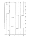
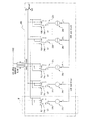
図12は、上記した特許文献1に記載されているデジタル/RF変換器1、2の構成を示した回路図である。デジタル/RF変換器1、2は、同じ構成を有している。このため、図12中にはデジタル/RF変換器1、2の構成にあたる部分を単に「DRC」と示す。また、図12の説明においても、デジタル/RF変換器1、2を区別せず、単にデジタル/RF変換器と記す。
FIG. 12 is a circuit diagram showing the configuration of the digital /
デジタル/RF変換器は、LSB(Least Significant Bit)側の信号を処理するブロックと、MSB(Most Significant Bit)側の信号を処理するブロックと、を少なくとも備えている。LSB側のブロックは、ユニットブロックがバイナリで重み付けされた電流源280、281、…28kと、ギルバートセル型に配置されたローカル信号用スイッチ220、221、…22kと、データ信号用スイッチ240、241、…24kとで構成されている。1つの電流源と、この電流源に対応して配置された1組のローカル信号用スイッチ、データ信号用スイッチを、以降ユニットブロックとも記す。図12では、1つのユニットブロックに符号u´を付して示す。
The digital / RF converter includes at least a block for processing a signal on the LSB (Least Significant Bit) side and a block for processing a signal on the MSB (Most Significant Bit) side. The block on the LSB side includes
また、MSB(Most Significant Bit)側のブロックは、同じ値に重み付けされた電流源290と、ギルバートセル型に配置されたローカル信号用スイッチ230とデータ信号用スイッチ260とが必要なビット分並列に接続された構成を有している。このような構成により、特許文献1に記載された直接RF変調送信器では、デジタル/アナログ変換と周波数掛算とを同時に行うことができる。なお、図12に示した例では、デジタル/RF変換器の外部に設けられた外部負荷によって全ユニットブロックの電流出力が電圧変換されることとなっている。
Further, the MSB (Most Significant Bit) side block includes a
図13は、デジタル/RF変換器の一般的な動作を説明するための図である。このような回路には、RF信号、デジタルベースバンド信号が入力される。入力されたRF信号は、デジタルベースバンド信号によって変調されて出力される。変調された信号は、デジタルベースバンド信号が切り替わるタイミングで送信キャリア波の位相を反転した信号となる。 FIG. 13 is a diagram for explaining a general operation of the digital / RF converter. An RF signal and a digital baseband signal are input to such a circuit. The input RF signal is modulated by a digital baseband signal and output. The modulated signal is a signal obtained by inverting the phase of the transmission carrier wave at the timing when the digital baseband signal is switched.
図14は、図12に示したデジタル/RF変換器のユニットブロックをN型のMOS(Metal Oxide Semiconductor)トランジスタを使って構成した例を示した図である。図14に示したデジタル/RF変換器は、MOSトランジスタ141〜147を含んでいる。MOSトランジスタ147は、定電流源を構成しており、ゲート電圧が適切にバイアスされることによって定電流を生成している。MOSトランジスタ147によって生成された電流は、MOSトランジスタ141〜146によって構成される、いわゆるギルバートセル型のミキサ回路に供給される。
FIG. 14 is a diagram showing an example in which the unit block of the digital / RF converter shown in FIG. 12 is configured using an N-type MOS (Metal Oxide Semiconductor) transistor. The digital / RF converter shown in FIG. 14 includes MOS transistors 141-147. The
図14に示した構成のデジタル/RF変換器では、送信キャリア波の周波数で振動する差動入力信号LO+、LO−によって周波数変換された、デジタルベースバンド信号VLN+、VLN−に応じた電流が、差動出力電流IN、IXNとして出力される。
ここで入力信号LO+、LO−が入力される差動対を構成するMOSトランジスタ145、146のゲート幅Wについて説明する。
In the digital / RF converter having the configuration shown in FIG. 14, the current corresponding to the digital baseband signals V LN + and V LN− frequency-converted by the differential input signals LO + and LO− oscillating at the frequency of the transmission carrier wave. Are output as differential output currents I N and I XN .
Here, the gate width W of the
全てのユニットブロックにおいて、MOSトランジスタ145、146のゲート長Lを同じにし、図12に示したLSB側のMOSトランジスタのゲート幅WをW0、電流値をI0とする。このとき、LSB+1ビット目のユニットブロックを流れる電流の電流値が2倍となるため、電流値は2×I0となる。このとき、MOSのバイアス状態を揃えるためには、MOSトランジスタ145、146のゲート幅Wを2×W0とする。
In all the unit blocks, the
ここで、5ビットのデジタル/RF変換器を、全てバイナリ型で構成した場合のMOSトランジスタ145、146のゲート面積の総和は、W0+2×W0+4×W0+8×W0+16×W0=31×W0となる。図11に示したデジタル/RF変換器1、2のユニットブロックに図14の回路を適用したとき、MOSトランジスタ145、146には、図11の2分周器3から出力される差動ローカル信号TxLoI+、TxLoI−、TxLoQ+、TxLoQ−のうちのいずれかを出力する端子と接続される。このため、MOSトランジスタ145、146は、2分周器3にとっては容量性の負荷と見なされる。負荷の大きさは、MOSトランジスタ145、146のゲート面積に比例して増大する。
Here, the total gate area of the
高周波回路における2分周器では、容量性負荷の増大は、一般的に消費電流の増大を招く。このため、図11に示した直接RF変調送信器では、容量性負荷を小さくできるため、MOSトランジスタ145、146のゲート面積は小さいほど好ましい。
次に、図14に示したユニットブロックで必要な電源電圧Vddについて説明する。この説明では、差動入力信号LO+、LO−のうち、入力信号LO+は正、入力信号LO−は負の状態であるとする。また、デジタルベースバンド信号VLN+、VLN−のうち、デジタルベースバンド信号VLN+は正、デジタルベースバンド信号VLN−は負の状態であるとする。すなわち、以下の説明では、MOSトランジスタ147で発生した定電流が、MOSトランジスタ145、141を経由して出力に流れる場合を想定している。
In the frequency divider in the high frequency circuit, an increase in capacitive load generally causes an increase in current consumption. For this reason, in the direct RF modulation transmitter shown in FIG. 11, the capacitive load can be reduced. Therefore, the gate areas of the
Next, the power supply voltage Vdd necessary for the unit block shown in FIG. 14 will be described. In this description, it is assumed that the input signal LO + is positive and the input signal LO− is negative among the differential input signals LO + and LO−. Of the digital baseband signals V LN + and V LN− , the digital baseband signal V LN + is positive and the digital baseband signal V LN− is negative. That is, in the following description, it is assumed that a constant current generated in the
上記した状態において、MOSトランジスタ141、145、147各々の閾値電圧をVtnとし、MOSトランジスタ141のオーバードライブ電圧をVov1´、MOSトランジスタ145のオーバードライブ電圧をVov5´、MOSトランジスタ147のオーバードライブ電圧をVov7´とする。ここでオーバードライブ電圧とはMOSトランジスタのゲート・ソース間電圧から閾値電圧を引いた電圧であり、MOSトランジスタが飽和領域で動作するためには、ソース・ドレイン間電圧がオーバードライブ電圧以上であることが必要である。
In the above state, the threshold voltages of the
高速動作が必要なアナログ回路において、MOSトランジスタはトランスコンダクタンスが高く、増幅動作に向いた飽和領域で動作させることが望ましい。ここで、図14に示したユニットブロックにおいて、シングルエンドのゼロ−ピーク電圧振幅がV0必要なとき、MOSトランジスタ141,145,147が飽和領域で動作するための必要最低限の電源電圧Vdd´は、数式(1)で示される。
Vdd´ > Vo+Vov1´+Vov5´+Vov7´ …式(1)
ここで、出力電圧は電源電圧Vdd´を中心として電源電圧Vdd´+V0からVdd´−V0の間で変化すると想定している。定電流源用のMOSトランジスタ147の電流値をI0とすると、このユニットブロックで消費される消費電力はVdd´×I0となる。携帯型の送信器等では、その消費電力が蓄電池の放電時間に影響を与えるため、小さいほど好ましい。図14に示したユニットブロックの消費電力は、MOSトランジスタ141、145、157のオーバードライブ電圧を小さくすることによって数式上は削減可能である。
In an analog circuit that requires high-speed operation, a MOS transistor has a high transconductance and is preferably operated in a saturation region suitable for an amplification operation. Here, in the unit block shown in FIG. 14, when the single-ended zero-peak voltage amplitude is V0, the minimum necessary power supply voltage Vdd ′ for operating the
Vdd '> Vo + Vov1' + Vov5 '+ Vov7' (1)
Here, it is assumed that the output voltage changes between the power supply voltage Vdd ′ + V0 and Vdd′−V0 around the power supply voltage Vdd ′. If the current value of the constant current
しかしながら、オーバードライブ電圧を小さくするためには、MOSトランジスタのゲート幅Wとゲート長Lの比であるW/L値を大きく設計する必要がある。しかし、定電流源用のMOSトランジスタ147では、サイズのばらつき抑止や熱雑音低減の観点からオーバードライブ電圧を小さくすることは好ましくない。MOSトランジスタの141、142、143、144、145、146に関しては、通常は、Lはプロセスの最小値で設計されることを考慮すると、ゲート幅Wを大きくすることになる。ゲート幅Wの拡大は、W×Lで示されるMOSトランジスタのゲート面積の増大を招く。
However, in order to reduce the overdrive voltage, it is necessary to design a large W / L value, which is the ratio of the gate width W to the gate length L of the MOS transistor. However, in the
ゲート面積の増大は、その前段回路(例えば2分周器)の容量性負荷が増大し、デジタル/RF変換器の消費電流増大を招くため好ましくない。つまり、従来技術では、低電源電圧化による低消費電力化と、前段回路への容量負荷軽減による低消費電流化による低消費電力化とがトレードオフの関係にある。
本発明は、以上の点に鑑みてなされたものであり、消費電力をより省力化することができる直接RF変調送信器を提供することを目的とする。
An increase in the gate area is not preferable because the capacitive load of the preceding circuit (for example, the frequency divider 2) increases and causes an increase in current consumption of the digital / RF converter. That is, in the prior art, there is a trade-off relationship between lower power consumption by lowering power supply voltage and lower power consumption by lowering current consumption by reducing capacitive load on the previous circuit.
The present invention has been made in view of the above points, and an object thereof is to provide a direct RF modulation transmitter capable of further saving power consumption.
本発明の直接RF変調送信器は、1ビットのデジタルベースバンドデータの正転データと当該正転データの反転データとを入力し、第1RF信号と当該第1RF信号と位相が180度異なる第2RF信号とを入力し、前記正転データおよび前記反転データが前記第1RF信号および前記第2RF信号によって周波数変換された第1電圧信号と当該第1電圧信号の差動信号である第2電圧信号とを出力する受動ミキサ回路と、定電流源と、前記定電流源によって生成された定電流を、前記受動ミキサ回路から出力された前記第1電圧信号、第2電圧信号に応じて第1出力信号と、当該第1電圧信号の差動信号である第2出力信号とに変換する差動対素子と、を有するユニットブロックを複数個含み、複数ビットの前記デジタルベースバンドデータからなるデジタルベースバンド信号によって前記第1RF信号及び前記第2RF信号を変調し、前記各ユニットブロックからの出力信号を加算すること特徴とすることを特徴とする。 Direct RF modulator transmitter of the present invention inputs the inverted data of the forward data and those positive inversion data of 1-bit digital baseband data, the 1RF signals and those said 1RF signals and a phase difference of 180 degrees enter the second 2RF signal, the forward data and said inverted second data is a differential signal of a first voltage signal and those first voltage signal frequency-converted by said first 1RF signal and the second 2RF signal A passive mixer circuit that outputs a voltage signal, a constant current source, and a constant current generated by the constant current source according to the first voltage signal and the second voltage signal output from the passive mixer circuit. A plurality of unit blocks each having a single output signal and a differential pair element that converts a second output signal that is a differential signal of the first voltage signal, and a plurality of bits of the digital baseband data. Modulating the first 1RF signal and the second 2RF signal by a digital baseband signal consisting of, characterized by, wherein adding the output signals from the respective unit blocks.
また、本発明の直接RF変調送信器は、上記した発明において、前記受動ミキサ回路が、ソースに前記1ビットのデジタルベースバンドデータの正転データが入力され、ゲートに前記第1RF信号が入力され、ドレインが前記差動対を構成する第5トランジスタ(例えば図1に示したMOSトランジスタ105)のゲートに接続される第1トランジスタ(例えば図1に示したMOSトランジスタ101)と、ソースに前記1ビットのデジタルベースバンドデータの正転データが入力され、ゲートに前記第2RF信号が入力され、ドレインが前記差動対を構成する第6トランジスタ(例えば図1に示したMOSトランジスタ106)のゲートに接続される第2トランジスタ(例えば図1に示したMOSトランジスタ102)と、ソースに前記1ビットのデジタルベースバンドデータの反転データが入力され、ゲートに前記第2RF信号が入力され、ドレインが前記第5トランジスタのゲートに接続される第3トランジスタ(例えば図1に示したMOSトランジスタ103)と、ソースに前記1ビットのデジタルベースバンドデータの反転データが入力され、ゲートに前記第1RF信号が入力され、ドレインが前記第6トランジスタのゲートに接続される第4トランジスタ(例えば図1に示したMOSトランジスタ104)と、を含むことが望ましい。
The direct RF modulation transmitter according to the present invention is the direct RF modulation transmitter according to the above-described invention, wherein the passive mixer circuit receives the normal data of the 1-bit digital baseband data as a source and the first RF signal as a gate. The first transistor (for example, the
また、本発明の直接RF変調送信器は、上記した発明において、前記定電流源が、前記第5トランジスタのソースと前記第6トランジスタのソースの共通接点に接続されることが望ましい。
また、本発明の直接RF変調送信器は、上記した発明において、前記第1トランジスタ、前記第2トランジスタ、前記第3トランジスタ、前記第4トランジスタが、N型MOSトランジスタで構成されることが望ましい。
In the direct RF modulation transmitter according to the aspect of the invention described above, it is preferable that the constant current source is connected to a common contact point between the source of the fifth transistor and the source of the sixth transistor.
In the direct RF modulation transmitter according to the present invention, it is preferable that the first transistor, the second transistor, the third transistor, and the fourth transistor are N-type MOS transistors in the above-described invention.
また、本発明の直接RF変調送信器は、上記した発明において、前記第1トランジスタ、前記第2トランジスタ、前記第3トランジスタ、前記第4トランジスタが、P型MOSトランジスタで構成されることが望ましい。 In the direct RF modulation transmitter according to the present invention, it is preferable that the first transistor, the second transistor, the third transistor, and the fourth transistor are P-type MOS transistors in the above-described invention.
上記した本発明の直接RF変調送信器は、パッシブミキサと差動対の組み合わせ回路をギルバートセルの替わりに用いることで、低電源電圧化による低消費電力化と、前段回路への容量負荷軽減による低消費電流化による低消費電力化を両立させることができる。そのため、このような送信器を半導体集積回路で実現した場合、消費電力を従来に比べ少なくすることができる。
以上のことから、本発明によれば、消費電力をいっそう省力化することができる直接RF変調送信器を提供することができる。
The above-described direct RF modulation transmitter of the present invention uses a combination circuit of a passive mixer and a differential pair instead of a Gilbert cell, thereby reducing power consumption by lowering the power supply voltage and reducing capacitive load on the previous circuit. Low power consumption can be achieved by reducing current consumption. Therefore, when such a transmitter is realized by a semiconductor integrated circuit, power consumption can be reduced as compared with the conventional one.
From the above, according to the present invention, it is possible to provide a direct RF modulation transmitter capable of further saving power consumption.
(第1実施形態)
以下、本発明の直接RF変調送信器の第1実施形態、第2実施形態、第3実施形態を説明する。
・回路構成
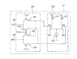
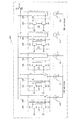
図1は、第1実施形態の直接RF変調送信器の回路構成を説明するための図であって、直接RF変調送信器に含まれるデジタル/RF変換器の1つのユニットブロックu1を示している。なお、ユニットブロックとは、直接RF変調送信器に含まれるデジタル/RF変換器を構成する1つの電流源と、この電流源に対応して設けられた複数のスイッチとを含むユニットを指す。
(First embodiment)
Hereinafter, a first embodiment, a second embodiment, and a third embodiment of the direct RF modulation transmitter of the present invention will be described.
Circuit Configuration FIG. 1 is a diagram for explaining a circuit configuration of the direct RF modulation transmitter according to the first embodiment. One unit block u1 of the digital / RF converter included in the direct RF modulation transmitter is illustrated. Show. The unit block refers to a unit including one current source constituting a digital / RF converter included in the direct RF modulation transmitter and a plurality of switches provided corresponding to the current source.
ユニットブロックu1は、MOSトランジスタ101、102、103、104、105、106、107を含んでいる。第1実施形態では、MOSトランジスタ101〜107は、N型MOSトランジスタである。MOSトランジスタ101〜104は、受動ミキサ回路100を構成する。また、MOSトランジスタ105〜107は、電流出力回路150を構成する。
The unit block u1 includes
MOSトランジスタ101、102のソースは、端子108に接続されている。また、MOSトランジスタ103、104のソースは端子109に接続されている。端子108は、受動ミキサ回路100に1ビットベースバンドデータDを入力する。端子109は、受動ミキサ回路100に1ビットベースバンドデータDの反転データDNを入力する。
また、受動ミキサ回路100のMOSトランジスタ101、104のゲートには、差動ローカル信号TxLoI+が入力される。MOSトランジスタ102、103のゲートには、差動ローカル信号TxLoI−が入力される。差動ローカル信号TxLoI+、TxLoI−は、送信キャリア波の周波数で振動する。
The sources of the
The differential local signal TxLoI + is input to the gates of the
MOSトランジスタ105、106は、ソース同士が接続されて差動対を構成する。MOSトランジスタのドレイン105、106には、MOSトランジスタ107のドレインが接続されている。MOSトランジスタ107のゲートには電圧Vbが供給され、電圧Vbに対応する量の電流がMOSトランジスタ105、106に供給される。このようなMOSトランジスタ107は、定電流源として機能する。
The
MOSトランジスタ105のゲートには、受動ミキサ回路100のMOSトランジスタ101、103のドレインから出力される出力電圧Vpが入力される。MOSトランジスタ106のゲートには、MOSトランジスタ104、102のドレインから出力される出力電圧Vnが入力される。
MOSトランジスタ105、106は、MOSトランジスタ107から供給された一定の電流を、出力端子110、111に振り分ける。出力端子110、111に振り分けられた電流は、ユニットブロックu1の外部で電流負荷回路に入力され、電圧に変換される。この結果、MOSトランジスタ105のドレインと接続する出力端子110には出力電圧Vonがかかる。また、MOSトランジスタ106のドレインと接続する出力端子111には出力電圧Vopがかかる。
The output voltage Vp output from the drains of the
The
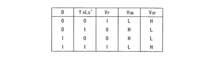
図2は、1ビットベースバンドデータD、差動ローカル信号TxLoI+、出力電圧Vp、出力電圧Von、Vopを示した図である。図2に示したように、出力電圧Vpは、入力される1ビットベースバンドデータDと、差動ローカル信号TxLoI+の極性にしたがって「1」または「0」の値をとる。1ビットベースバンドデータDは、受動ミキサ回路100において、差動ローカル信号TxLoI+、TxLoI−によって周波数変換されたとみなすことができる。
FIG. 2 is a diagram showing 1-bit baseband data D, differential local signal TxLoI +, output voltage Vp, output voltages Von, and Vop. As shown in FIG. 2, the output voltage Vp takes a value of “1” or “0” according to the input 1-bit baseband data D and the polarity of the differential local signal TxLoI +. The 1-bit baseband data D can be regarded as frequency-converted by the differential local signals TxLoI + and TxLoI− in the
・電源電圧
第1実施形態の直接RF変調送信器において、電流出力回路150を構成する全てのMOSトランジスタが飽和領域で動作するための必要最低限の電源電圧Vddは、数式(2)で表される。
Vdd >Vo+Vov5+Vov7 …式(2)
式(2)において、Vov5はMOSトランジスタ105のオーバードライブ電圧を指す。また、Vov7は、MOSトランジスタ107のオーバードライブ電圧を指す。また、受動ミキサ回路100の出力電圧Vpの極性がハイであり、Vnの極性がローであり、ユニットブロックの出力においてシングルエンドのゼロ−ピーク電圧振幅V0が必要であるものとした。
Power supply voltage In the direct RF modulation transmitter according to the first embodiment, the minimum power supply voltage Vdd required for all the MOS transistors constituting the
Vdd> Vo + Vov5 + Vov7 (2)
In Equation (2), Vov5 indicates the overdrive voltage of the
上記した式(2)と、図14に示した従来のユニットブロックの電源電圧を示す式(1)とを比較すると、第1実施形態のユニットブロックに必要な電源電圧Vddは、従来のユニットブロックに必要な電源電圧Vdd´よりもVov1´だけ小さいことが分かる。なお、図1に示したMOSトランジスタ107が、図14に示したMOSトランジスタ147と同じ設計条件、同じプロセス条件で製造されたものとする。図1に示したMOSトランジスタ105,106が図14に示したMOSトランジスタ145、146と同じ設計条件、同じプロセス条件で製造されたものとする。
さらに、第1実施形態では、受動ミキサ回路100の電源、グランド間に電流が流れる経路が無いため、受動ミキサ回路100では電流が消費されない。このため、図1に示したユニットブロックを含む第1実施形態の直接RF変調送信器は、従来の直接RF変調送信器と比較していっそうの低電源電圧化による低消費電力化が可能である。
Comparing the above equation (2) with equation (1) showing the power supply voltage of the conventional unit block shown in FIG. 14, the power supply voltage Vdd required for the unit block of the first embodiment is It can be seen that Vov1 'is smaller than the power supply voltage Vdd' required for the above. It is assumed that the
Furthermore, in the first embodiment, since there is no path for current to flow between the power supply and ground of the
・前段回路への影響(第1実施形態の効果)
次に、ユニットブロックを含むデジタル/RF変換器の前段回路(例えば2分周器)に対する、第1実施形態の影響について説明する。
図1に示した受動ミキサ回路100を構成するMOSトランジスタ101〜104は、そのゲート、ソース間電圧が十分高くなってオーバードライブ電圧が正になると、ソース、ドレイン間が電気的に接続される。そして、ソース、ドレイン間の電圧が等しくするように動作する。このような動作は、受動ミキサ回路100を構成するMOSトランジスタ101〜104が、正のオーバードライブ電圧のときに、基本的に三極管領域において動作することを意味する。
・ Effects on the previous circuit (effects of the first embodiment)
Next, the influence of the first embodiment on the pre-stage circuit (for example, a frequency divider of 2) of the digital / RF converter including the unit block will be described.
The
受動ミキサ回路100に入力される1ビットベースバンドデータD、反転データDNは、差動ローカル信号TxLo+、TxLo−によって周波数変換される。周波数変換された信号は、差動対を構成するMOSトランジスタ105、106のゲートに入力される。MOSトランジスタ105のゲートに出力される出力電圧Vpの変化速度は、トランジスタ101もしくはトランジスタ103のオーバードライブ電圧が正の場合の抵抗成分と、トランジスタ105のゲートの容量成分によって制限される。
The 1-bit baseband data D and the inverted data DN input to the
式(3)は、所望の周波数をf、MOSトランジスタ101、103のゲート幅をW、ゲート長をL、トランジスタ101、103のオーバードライブ電圧が負から正に遷移するときの、ソース、ドレイン電圧をVds、MOSトランジスタ105のゲート容量CL、キャリアの移動度をμ、単位面積当たりのゲート容量をCoxとしたときの、必要なW/L比の最小値を示している。ここでfは送信キャリア周波数よりも高い周波数を設定することが望ましい。
W/L=2・π・CL・f/(μ・Cox・Vds) …式(3)
Equation (3) is the source and drain voltages when the desired frequency is f, the gate width of the
W / L = 2 · π · CL · f / (µ · Cox · Vds) Equation (3)
MOSトランジスタのゲート容量は、ゲート幅Wとゲート長LとCoxから計算され、式(4)に示される。図14に示したMOSトランジスタ145のゲート幅Wを20[um]、ゲート長Lを0.13[um]、キャリア移動度μを100[uA/V2]、Coxを10[fF/um2]とする。このとき、MOSトランジスタ145のゲート容量CLは、式(4)から26[fF]と算出される。この結果は、前段回路からの信号LO+が26[fF]の容量を駆動することを意味する。
CL=Cox・W・L 式(4)
次に、図1の差動対を構成するMOSトランジスタ105が、図14のトランジスタ145と同一サイズ、同じ単位面積当たりのゲート容量Coxを有し、MOSトランジスタ105と図14に示したMOSトランジスタ145とはゲート容量CLが等しいとする。さらに、図1に示したMOSトランジスタ107と図14に示したMOSトランジスタ147は同一値の定電流を生成するものとする。
The gate capacity of the MOS transistor is calculated from the gate width W, the gate length L, and Cox, and is shown in Equation (4). The gate width W of the
CL = Cox · W · L Formula (4)
Next, the
このとき、第1実施形態の受動ミキサ回路100を構成するトランジスタ101のW/Lの最小値は、f=2[GHz]、Vds=0.1[V]とすると、W/L=32.67と計算される。ここでL=0.13[um]とすると、W=4.25[um]となり、トランジスタ101のゲート容量は、Cox=10[fF/um2]とすると、5.52[fF]となる。
At this time, if the minimum value of W / L of the
一般に、1つの受動ミキサ回路100を構成するトランジスタ101〜104は、全て同じゲート幅とゲート長とを有するように設計される。これにより、前段の回路からのローカル差動信号TxLo+は、MOSトランジスタ101のゲート容量と、MOSトランジスタ104のゲート容量の合計値である11.04[fF]を駆動する。
以上のことから、第1実施形態の直接RF変調送信器は、そのユニットブロックの前段回路が駆動すべき容量が、従来技術よりも小さくなる。このため、第1実施形態の直接RF変調送信器は、従来よりも低い消費電力で駆動することができるようになる。
In general, the
From the above, in the direct RF modulation transmitter according to the first embodiment, the capacity to be driven by the preceding circuit of the unit block is smaller than that in the prior art. For this reason, the direct RF modulation transmitter of the first embodiment can be driven with lower power consumption than in the prior art.
(第2実施形態)
・回路構成
図3は、本発明の第2実施形態の直接RF変調送信器の、ユニットブロックu2を説明するための図である。ユニットブロックu2は、MOSトランジスタ201、202、203、204、205、206を含んでいる。MOSトランジスタ201〜204は、P型MOSトランジスタであって、受動ミキサ回路200を構成する。MOSトランジスタ205、206は、NMOSトランジスタである。
(Second Embodiment)
Circuit Configuration FIG. 3 is a diagram for explaining the unit block u2 of the direct RF modulation transmitter according to the second embodiment of the present invention. The unit block u2 includes
さらに、ユニットブロックu2は、MOSトランジスタ205、206のソースに接続される定電流源207を含んでいる。MOSトランジスタ205、206、定電流源207は、電流出力回路250を構成する。
MOSトランジスタ201、202のソースは、端子208に接続されている。また、MOSトランジスタ203、204のソースは端子209に接続されている。端子208は、受動ミキサ回路200に1ビットベースバンドデータDを入力する。端子209は、受動ミキサ回路200に1ビットベースバンドデータDの反転データDNを入力する。
The unit block u2 further includes a constant
The sources of the
また、受動ミキサ回路200のMOSトランジスタ201、204のゲートには、差動ローカル信号TxLoI+が入力される。MOSトランジスタ202、203のゲートには、差動ローカル信号TxLoI−が入力される。差動ローカル信号TxLoI+、TxLoI−は、送信キャリア波の周波数で振動する。このとき、受動ミキサ回路200の出力電圧Vp、Vnは、入力される1ビットベースバンドデータDと差動ローカル信号TxLo+の極性から、図2に示した表の極性に従って出力される。
The differential local signal TxLoI + is input to the gates of the
図2に示したように、受動ミキサ回路200において、1ビットベースバンドデータDは、差動ローカル信号TxLo+、TxLo−によって周波数変換されるものとみなせる。受動ミキサ回路200の出力電圧Vpは、差動対を構成するMOSトランジスタ205のゲートに入力される。出力電圧Vnは、差動対を構成するMOSトランジスタ206のゲートに入力される。MOSトランジスタ205、206は、定電流源207によって生成された定電流を、出力端子210、211に振り分ける。このとき、定電流源207は適切にバイアスされている。
出力端子210、211に振り分けられた電流は、ユニットブロックu2の外部で電流負荷回路に入力され、電圧に変換される。
As shown in FIG. 2, in the
The current distributed to the
・電源電圧
第2実施形態の直接RF変調送信器の電流出力回路250は、図1に示したMOSトランジスタ107に代えて、定電流源207を設けた点でのみ第1実施形態と相違する。電流出力回路250は第1実施形態の電流出力回路150と同様に動作するため、その説明を省くものとする。
Power Supply Voltage The
・前段回路への影響
次に、ユニットブロックを含むデジタル/RF変換器の前段回路(例えば2分周器)に対する、第2実施形態の影響について説明する。
先ず、図3に示したMOSトランジスタ201のゲート幅Wとゲート長LのW/L比を、式(3)を使って計算する。差動対を構成するMOSトランジスタ205、206は、図1に示したMOSトランジスタ105、106と同一の設計条件、プロセス条件によって製造されているものとする。また、受動ミキサ回路200を構成するMOSトランジスタ201のVds=−0.1[V]、キャリア移動度μ=−40[uA/V2]とする。この他の条件は、第1実施形態のMOSトランジスタ101のW/L比を計算するにあたって式(3)に入力されたものと同じであるものとする。
Influence on the front-stage circuit Next, the influence of the second embodiment on the front-stage circuit (for example, the frequency divider 2) of the digital / RF converter including the unit block will be described.
First, the W / L ratio between the gate width W and the gate length L of the
このような計算により、MOSトランジスタ201のW/L比は、81.68となる。ここでL=0.13[um]とするとW=10.62[um]となる。また、MOSトランジスタ201の単位面積当たりのゲート容量Cox=10[fF/um2]とすると、MOSトランジスタ201のゲート容量CLは、式(4)から13.80[fF]となる。したがって、第2実施形態では、前段回路から入力される差動ローカル信号TxLo+が駆動する容量は、27.6[fF]となる。この値は図14に示した入力信号LO+が26[fF]駆動する容量とほぼ等しい。本計算はf=2[GHz]として計算を行ったが、より低い周波数を想定した場合、必要なW/L値が小さくなるため、ゲート容量の値をより小さくすることが可能である。
By such calculation, the W / L ratio of the
・定電流源への影響
次に、受動ミキサ回路200の出力電圧変化の挙動が、受動ミキサ回路200と接続される電流出力回路250に与える影響を説明する。
(1)第1実施形態について(比較例)
第2実施形態と比較するため、先ず、受動ミキサ回路100を構成するMOSトランジスタに、NMOSトランジスタを使った第1実施形態における定電流源への影響について説明する。
NMOSトランジスタがスイッチとしてオン状態となる条件は、式(5)によって表される。
Vgs−Vtn>0 式(5)
Influence on Constant Current Source Next, the influence of the behavior of the output voltage change of the
(1) About 1st Embodiment (comparative example)
For comparison with the second embodiment, first, the influence on the constant current source in the first embodiment in which an NMOS transistor is used as the MOS transistor constituting the
The condition that the NMOS transistor is turned on as a switch is expressed by Expression (5).
Vgs−Vtn> 0 Formula (5)
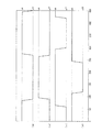
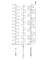
ここで、VgsはMOSトランジスタのゲート、ソース間電圧であり、Vtnは閾値電圧である。Vtn=0.5とし、図1に示した1ビットデジタル信号D、反転データDN、差動ローカル信号TxLo+、TxLo−の電圧が図4のように変化したとする。図4の縦軸は信号の電圧レベルを示し、横軸は時間を示している。曲線aは差動ローカル信号TxLo+を示し、曲線bは差動ローカル信号TxLo−を示している。直線cは1ビットデジタル信号Dを示し、直線dは反転データDNを示している。 Here, Vgs is a gate-source voltage of the MOS transistor, and Vtn is a threshold voltage. Assume that Vtn = 0.5, and the voltages of the 1-bit digital signal D, the inverted data DN, and the differential local signals TxLo + and TxLo− shown in FIG. 1 have changed as shown in FIG. The vertical axis in FIG. 4 indicates the voltage level of the signal, and the horizontal axis indicates time. A curve a indicates the differential local signal TxLo +, and a curve b indicates the differential local signal TxLo−. A straight line c represents the 1-bit digital signal D, and a straight line d represents the inverted data DN.
図4に示すように各信号の電圧レベルが変化する場合、MOSトランジスタ101〜104は、図5に示すようにオン、オフされる。図5(a)はMOSトランジスタ101のオン、オフ状態を示す。図5の縦軸は各MOSトランジスタのオン、オフ状態を示し、横軸は時間を示す。図5(b)はMOSトランジスタ102のオン、オフ状態を、(c)はMOSトランジスタ103のオン、オフ状態を、(d)はMOSトランジスタ104のオン、オフ状態をそれぞれ示している。図5(a)〜(d)において、ハイ区間がMOSトランジスタのオンを表し、ロー区間がMOSトランジスタのオフを表す。
When the voltage level of each signal changes as shown in FIG. 4, the
図6は、図5に示したようにMOSトランジスタ101〜104がオン、オフ動作したときの、受動ミキサ回路100の出力電圧Vp、Vnの変化を示している。図6の縦軸は出力電圧のレベルであり、横軸は時間である。図6において、プロット「□」は出力電圧Vpを示している。また、プロット「×」は出力電圧Vnを示している。
出力電圧Vpは、MOSトランジスタ101がオン、MOSトランジスタ103がオフの場合、1ビットベースバンドデータDにしたがう電圧となる。また、MOSトランジスタ101がオフ、MOSトランジスタ103がオンの場合、反転データDNにしたがう電圧となる。また、MOSトランジスタ101がオン、MOSトランジスタ103がオンの場合、1ビットベースバンド信号にしたがう電圧と、反転データDNにしたがう電圧の中間電圧となる。さらに、MOSトランジスタ101がオフ、MOSトランジスタ103がオフになる状態は、差動ローカル信号TxLo+、TxLo−の動作点を適切にバイアスすることによって回避される。
FIG. 6 shows changes in the output voltages Vp and Vn of the
The output voltage Vp is a voltage according to the 1-bit baseband data D when the
出力電圧Vnは、MOSトランジスタ102がオン、MOSトランジスタ104がオフの場合、1ビットベースバンドデータDにしたがう電圧となる。また、MOSトランジスタ102がオフ、MOSトランジスタ104がオンの場合、反転データDNにしたがう電圧となる。また、MOSトランジスタ102がオン、MOSトランジスタ104がオンの場合、1ビットベースバンド信号にしたがう電圧と、反転データDNにしたがう電圧の中間電圧となる。さらに、MOSトランジスタ102がオフ、MOSトランジスタ104がオフになる状態は、差動ローカル信号TxLo+、TxLo−の動作点を適切にバイアスすることによって回避される。
The output voltage Vn is a voltage according to the 1-bit baseband data D when the
NMOSトランジスタで構成された受動ミキサ回路100は、図4に示した入力状態のとき、ソース電圧の低いMOSトランジスタ103、104の方が、MOSトランジスタ101、102よりもオン状態に遷移し易い。このため図6に示した入力電圧Vp、Vnのように、ハイ電圧出力(図6の縦軸1.5)よりもロー電圧出力(図6の縦軸1.0)の時間が長くなり、瞬間的にVpがロー電圧でVnもロー電圧という状況が発生し得る。
In the
出力電圧Vp、Vnは、受動ミキサ回路100の後段に設置される電流出力回路150のMOSトランジスタ105、106のゲート電圧になる。このため、出力電圧Vp、Vnが共にロー電圧になる、という状況は、定電流源として機能するMOSトランジスタ107のドレイン電圧を瞬間的に低下させる場合がある。MOSトランジスタ107のドレイン電圧が瞬間的に低下すると、MOSトランジスタ107の状態は、瞬間的に飽和領域から三極間領域に遷移する。このとき、MOSトランジスタ107から出力される電流の値は、本来期待されている値から外れる可能性がある。電流値が期待値から瞬間的にずれることは、出力における歪みとなることもある。
The output voltages Vp and Vn are the gate voltages of the
(2)第2実施形態について(第2実施形態の効果)
次に、図3に示した受動ミキサ回路200の出力の電圧変化の挙動が、電流出力回路250のMOSトランジスタ205、206と定電流源207に与える影響を説明する。
受動ミキサ回路200を構成するMOSトランジスタ201〜204は、PMOSトランジスタである。PMOSトランジスタがスイッチとしてオン状態となる条件は、式(6)によって与えられる。式(6)において、Vgsはトランジスタのゲート、ソース間電圧であり、VtpはPMOSトランジスタの閾値電圧である。
Vgs−Vtp <0 …式(6)
(2) Second Embodiment (Effects of Second Embodiment)
Next, the influence of the voltage change behavior of the output of the
The
Vgs−Vtp <0 Equation (6)
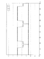
図7は、図3に示したユニットブロックu2における、1ビットベースバンドデータD、反転データDN、差動ローカル信号TxLo+、TxLo−の電圧の変化の状態を示した図である。図7の縦軸は、各信号の電圧レベルを示し、横軸は時間を示している。図7中に示した曲線aは差動ローカル信号TxLo+を示し、曲線bは差動ローカル信号TxLo−を示している。直線cは1ビットデジタル信号Dを示し、直線dは反転データDNを示している。なお、図7に示した状態では、閾値電圧Vtpが、−0.5Vであるものとする。 FIG. 7 is a diagram illustrating a state of voltage change of the 1-bit baseband data D, the inverted data DN, and the differential local signals TxLo + and TxLo− in the unit block u2 illustrated in FIG. The vertical axis in FIG. 7 indicates the voltage level of each signal, and the horizontal axis indicates time. A curve a shown in FIG. 7 indicates the differential local signal TxLo +, and a curve b indicates the differential local signal TxLo−. A straight line c represents the 1-bit digital signal D, and a straight line d represents the inverted data DN. In the state shown in FIG. 7, the threshold voltage Vtp is assumed to be −0.5V.
図7に示すように各信号の電圧レベルが変化する場合、MOSトランジスタ201〜204は、図8に示すようにオン、オフされる。図8の縦軸は各MOSトランジスタのオン、オフ状態を示し、横軸は時間を示す。図8(a)はMOSトランジスタ201のオン、オフ状態を示す。図8(b)はMOSトランジスタ202のオン、オフ状態を、(c)はMOSトランジスタ203のオン、オフ状態を、(d)はMOSトランジスタ204のオン、オフ状態をそれぞれ示している。図8(a)〜(d)において、ハイ区間がMOSトランジスタのオンを表し、ロー区間がMOSトランジスタのオフを表す。
When the voltage level of each signal changes as shown in FIG. 7, the
図9は、図3に示したMOSトランジスタ201〜204が図8に示したようにオン、オフ動作したときの、受動ミキサ回路200の出力電圧Vp、Vnの変化を示している。図9の縦軸は出力電圧のレベルであり、横軸は時間である。図9において、プロット「□」は出力電圧Vpを示している。また、プロット「×」は出力電圧Vnを示している。
出力電圧Vpは、MOSトランジスタ201がオン、MOSトランジスタ203がオフの場合、1ビットベースバンドデータDにしたがう電圧となる。また、MOSトランジスタ201がオフ、MOSトランジスタ203がオンの場合、反転データDNにしたがう電圧となる。また、MOSトランジスタ201がオン、MOSトランジスタ203がオンの場合、1ビットベースバンド信号にしたがう電圧と、反転データDNにしたがう電圧の中間電圧となる。さらに、MOSトランジスタ201がオフ、MOSトランジスタ203がオフになる状態は、差動ローカル信号TxLo+、TxLo−の動作点を適切にバイアスすることによって回避される。
FIG. 9 shows changes in the output voltages Vp and Vn of the
The output voltage Vp is a voltage according to the 1-bit baseband data D when the
PMOSトランジスタで構成された受動ミキサ回路200は、図7に示した入力状態のとき、ソース電圧の高いMOSトランジスタ201、202の方が、MOSトランジスタ203、204よりもオン状態に遷移し易い。このため図9に示した出力電圧Vp、Vnのように、ロー電圧出力よりもハイ電圧出力の時間が長くなる。そのため、受動ミキサ回路200をNMOSトランジスタで構成した場合と異なり、Vpがロー電圧でVnもロー電圧という状況は、瞬間的であっても発生しない。このため定電流源207の状態が瞬間的に飽和領域から三極間領域に遷移し、定電流源207から出力される電流が、本来期待されている値から外れることを防ぐことができる。
In the
(第3実施形態)
・回路構成
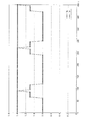
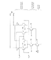
図10は、本発明の第3実施形態を説明するための図であって、実施形態3の直接RF変調送信器に含まれる、デジタル/RF変換器(図中、DRCと記す)の回路図である。デジタル/RF変換器は、LSB(Least Significant Bit)側の信号を処理するブロックと、MSB(Most Significant Bit)側の信号を処理するブロックとを備えている。LSB側のブロックは、ユニットブロックがバイナリで重み付けされた電流源300、301、…30kと、NMOSトランジスタで構成された差動対340、341、…34kと、ローカル信号用とデータ信号を周波数掛算するためのNMOSトランジスタで構成されたミキサ回路320、321、…32kと、で構成されている。
(Third embodiment)
Circuit Configuration FIG. 10 is a diagram for explaining a third embodiment of the present invention, and is a digital / RF converter (denoted as DRC in the figure) included in the direct RF modulation transmitter of the third embodiment. FIG. The digital / RF converter includes a block that processes a signal on the LSB (Least Significant Bit) side and a block that processes a signal on the MSB (Most Significant Bit) side. The block on the LSB side is a unit of binary weighted
また、MSB(Most Significant Bit)側のブロックは、同じ値に重み付けされた電流源310と、NMOSトランジスタで構成された差動対350と、ローカル信号用とデータ信号をミキシングするためのNMOSトランジスタで構成されたミキサ回路330とが必要なビット分並列に接続された構成を有している。このような構成により、実施形態3のデジタル/RF変換器を有した直接RF変調送信器では、デジタル/アナログ変換と周波数掛算とを同時に行うことができる。なお、図10に示した例では、デジタル/RF変換器の外部に設けられた外部負荷によって全ユニットブロックの電流出力が電圧変換されることとなっている。
The MSB (Most Significant Bit) block includes a
ミキサ回路320、321、…32k、ミキサ回路320と差動対340、341、…304k、差動対350で構成される各回路は、第1実施形態で示したユニットブロックそのものである。
また、ミキサ回路320、321、…32k、ミキサ回路320を第2実施形態で説明した、PMOSトランジスタで構成された受動ミキサ回路に置き換えたデジタル/RF変換器回路を有した直接RF変調送信器においても、デジタル/アナログ変換と周波数掛算とを同時に行うことができる。
図10に示した第1実施形態、第2実施形態のユニットブロックに相当する構成から得られた電流は、図10に示すように、加算されて外部に出力される。
32k, the
In addition, in the direct RF modulation transmitter having a digital / RF converter circuit in which the
The currents obtained from the configurations corresponding to the unit blocks of the first and second embodiments shown in FIG. 10 are added and output to the outside as shown in FIG.
・電源電圧と前段回路への影響(実施形態3の効果)
図10に示した実施形態3のデジタル/RF変換器回路は、第1実施形態もしくは第2実施形態に記載のユニットブロックにより構成される。このため、第1実施形態、第2の実施形態において説明した通り、従来技術と比較し、低電圧化による低消費化に加え、前段回路の消費電流低減による低消費電力化が可能である。
・ Effect on power supply voltage and previous circuit (Effect of Embodiment 3)
The digital / RF converter circuit of the third embodiment shown in FIG. 10 is configured by the unit block described in the first embodiment or the second embodiment. Therefore, as described in the first embodiment and the second embodiment, it is possible to reduce the power consumption by reducing the current consumption of the previous circuit, in addition to the reduction of the power consumption by reducing the voltage, as compared with the prior art.
本発明の直接RF変調送信器は、消費電力が小さいため、特に携帯型の機器に適用することに適している。 Since the direct RF modulation transmitter of the present invention has low power consumption, it is particularly suitable for application to a portable device.
MOSトランジスタ 101〜107、201〜206
受動ミキサ回路 100、200
端子 108、109、208、209
出力端子 110、111、210、211
電流出力回路 150、250
定電流源 207、300〜30K、310
ミキサ回路 320〜32K、330
差動対 340〜34K、350
デジタル/RF変換器(DRC)1、2
2分周器 3
整合回路 4
パワーアンプ(PA) 5
ローカル信号用スイッチ 220〜22k、230
データ信号用スイッチ 240〜24k、260
定電流源 280〜28K、290
MOSトランジスタ 141〜147
MOS transistors 101-107, 201-206
Constant
Mixer circuit 320-32K, 330
Differential pair 340-34K, 350
Digital / RF converter (DRC) 1, 2
Divider by 2 3
Matching circuit 4
Power amplifier (PA) 5
Local signal switch 220-22k, 230
Data signal switch 240-24k, 260
Constant current source 280-28K, 290
MOS transistors 141-147
Claims (5)
定電流源と、
前記定電流源によって生成された定電流を、前記受動ミキサ回路から出力された前記第1電圧信号、第2電圧信号に応じて第1出力信号と、当該第1電圧信号の差動信号である第2出力信号とに変換する差動対素子と、
を有するユニットブロックを複数個含み、
複数ビットの前記デジタルベースバンドデータからなるデジタルベースバンド信号によって前記第1RF信号及び前記第2RF信号を変調し、前記各ユニットブロックからの出力信号を加算すること特徴とする直接RF変調送信器。 Inputs the inverted data of the forward data and those positive inversion data of 1-bit digital baseband data, the 1RF signals and those said 1RF signal and the phase inputs and 180 degrees different from the first 2RF signal, the positive and a passive mixer circuit outputting a second voltage signal is a differential signal of the rolling data and the inverted data is first voltage signal and those first voltage signal frequency-converted by said first 1RF signal and the second 2RF signal ,
A constant current source;
The constant current generated by the constant current source is a first output signal according to the first voltage signal and the second voltage signal output from the passive mixer circuit, and a differential signal of the first voltage signal. A differential pair element for converting to a second output signal;
A plurality of unit blocks having
A direct RF modulation transmitter, wherein the first RF signal and the second RF signal are modulated by a digital baseband signal composed of a plurality of bits of the digital baseband data, and an output signal from each unit block is added.
ソースに前記1ビットのデジタルベースバンドデータの正転データが入力され、ゲートに前記第1RF信号が入力され、ドレインが前記差動対を構成する第5トランジスタのゲートに接続される第1トランジスタと、
ソースに前記1ビットのデジタルベースバンドデータの正転データが入力され、ゲートに前記第2RF信号が入力され、ドレインが前記差動対を構成する第6トランジスタのゲートに接続される第2トランジスタと、
ソースに前記1ビットのデジタルベースバンドデータの反転データが入力され、ゲートに前記第2RF信号が入力され、ドレインが前記第5トランジスタのゲートに接続される第3トランジスタと、
ソースに前記1ビットのデジタルベースバンドデータの反転データが入力され、ゲートに前記第1RF信号が入力され、ドレインが前記第6トランジスタのゲートに接続される第4トランジスタと、
を含むこと特徴とする請求項1に記載の直接RF変調送信器。 The passive mixer circuit is:
A first transistor in which normal data of the 1-bit digital baseband data is input to a source, the first RF signal is input to a gate, and a drain is connected to a gate of a fifth transistor constituting the differential pair; ,
A non-inverting data of the 1-bit digital baseband data is input to a source; the second RF signal is input to a gate; and a drain is connected to a gate of a sixth transistor forming the differential pair; ,
A third transistor in which inverted data of the 1-bit digital baseband data is input to a source, the second RF signal is input to a gate, and a drain is connected to a gate of the fifth transistor;
A fourth transistor in which inverted data of the 1-bit digital baseband data is input to a source, the first RF signal is input to a gate, and a drain is connected to a gate of the sixth transistor;
The direct RF modulation transmitter of claim 1, comprising:
Priority Applications (1)
| Application Number | Priority Date | Filing Date | Title |
|---|---|---|---|
| JP2011187410A JP5551663B2 (en) | 2011-08-30 | 2011-08-30 | Direct RF modulation transmitter |
Applications Claiming Priority (1)
| Application Number | Priority Date | Filing Date | Title |
|---|---|---|---|
| JP2011187410A JP5551663B2 (en) | 2011-08-30 | 2011-08-30 | Direct RF modulation transmitter |
Publications (2)
| Publication Number | Publication Date |
|---|---|
| JP2013051494A JP2013051494A (en) | 2013-03-14 |
| JP5551663B2 true JP5551663B2 (en) | 2014-07-16 |
Family
ID=48013255
Family Applications (1)
| Application Number | Title | Priority Date | Filing Date |
|---|---|---|---|
| JP2011187410A Expired - Fee Related JP5551663B2 (en) | 2011-08-30 | 2011-08-30 | Direct RF modulation transmitter |
Country Status (1)
| Country | Link |
|---|---|
| JP (1) | JP5551663B2 (en) |
Family Cites Families (3)
| Publication number | Priority date | Publication date | Assignee | Title |
|---|---|---|---|---|
| US6980779B2 (en) * | 2003-11-20 | 2005-12-27 | Nokia Corporation | RF transmitter using digital-to-RF conversion |
| JP2009049585A (en) * | 2007-08-16 | 2009-03-05 | Renesas Technology Corp | Differential amplifier circuit, mixer circuit and receiver |
| US8615205B2 (en) * | 2007-12-18 | 2013-12-24 | Qualcomm Incorporated | I-Q mismatch calibration and method |
-
2011
- 2011-08-30 JP JP2011187410A patent/JP5551663B2/en not_active Expired - Fee Related
Also Published As
| Publication number | Publication date |
|---|---|
| JP2013051494A (en) | 2013-03-14 |
Similar Documents
| Publication | Publication Date | Title |
|---|---|---|
| US10008984B2 (en) | Apparatus and method for dynamically biased baseband current amplifier | |
| JPWO2012176250A1 (en) | Differential switch drive circuit and current steering type digital-to-analog converter | |
| US9503022B2 (en) | Balanced up-conversion mixer | |
| US20120256676A1 (en) | Mixer circuit | |
| US7463869B2 (en) | Low noise high isolation transmit buffer gain control mechanism | |
| US7868695B2 (en) | Differential amplifier | |
| US8847662B2 (en) | Mixer and associated signal circuit | |
| CN103684267B (en) | signal mixing circuit | |
| JP6446192B2 (en) | Transmitting apparatus and transmitting method | |
| JP5551663B2 (en) | Direct RF modulation transmitter | |
| US9197174B2 (en) | Analog baseband filter for radio transceiver | |
| KR100799227B1 (en) | Cascode Structured Power Amplifier for Amplitude Modulation | |
| Zimmermann et al. | Design of an RF-DAC in 65nm CMOS for multistandard, multimode transmitters | |
| CN105720923A (en) | Switching circuit, integrated circuit, active mixer circuit and method thereof | |
| JP4580882B2 (en) | Semiconductor integrated circuit | |
| US20080242253A1 (en) | Frequency converter and radio receiver using the same | |
| JP2012114610A (en) | Electronic circuit | |
| JP5204902B2 (en) | Transfer gate circuit and power combiner circuit, power amplifier circuit, transmitter and communication device using the same | |
| JP2006074380A (en) | Frequency mixer | |
| JP4909862B2 (en) | Frequency conversion circuit and receiver | |
| CN110120785B (en) | Low-power consumption mixer | |
| US10382036B2 (en) | High voltage switch | |
| JP2013223118A (en) | Mixer circuit | |
| JP5602791B2 (en) | Transmitter | |
| JP5524913B2 (en) | Transmitter |
Legal Events
| Date | Code | Title | Description |
|---|---|---|---|
| A621 | Written request for application examination |
Free format text: JAPANESE INTERMEDIATE CODE: A621 Effective date: 20130328 |
|
| A977 | Report on retrieval |
Free format text: JAPANESE INTERMEDIATE CODE: A971007 Effective date: 20131111 |
|
| A131 | Notification of reasons for refusal |
Free format text: JAPANESE INTERMEDIATE CODE: A131 Effective date: 20131126 |
|
| A521 | Written amendment |
Free format text: JAPANESE INTERMEDIATE CODE: A523 Effective date: 20140127 |
|
| TRDD | Decision of grant or rejection written | ||
| A01 | Written decision to grant a patent or to grant a registration (utility model) |
Free format text: JAPANESE INTERMEDIATE CODE: A01 Effective date: 20140520 |
|
| A61 | First payment of annual fees (during grant procedure) |
Free format text: JAPANESE INTERMEDIATE CODE: A61 Effective date: 20140522 |
|
| R150 | Certificate of patent or registration of utility model |
Ref document number: 5551663 Country of ref document: JP Free format text: JAPANESE INTERMEDIATE CODE: R150 |
|
| S531 | Written request for registration of change of domicile |
Free format text: JAPANESE INTERMEDIATE CODE: R313531 |
|
| R350 | Written notification of registration of transfer |
Free format text: JAPANESE INTERMEDIATE CODE: R350 |
|
| LAPS | Cancellation because of no payment of annual fees |