JP5516947B2 - Current sensor - Google Patents
Current sensor Download PDFInfo
- Publication number
- JP5516947B2 JP5516947B2 JP2009279415A JP2009279415A JP5516947B2 JP 5516947 B2 JP5516947 B2 JP 5516947B2 JP 2009279415 A JP2009279415 A JP 2009279415A JP 2009279415 A JP2009279415 A JP 2009279415A JP 5516947 B2 JP5516947 B2 JP 5516947B2
- Authority
- JP
- Japan
- Prior art keywords
- core
- magnetic
- current
- current sensor
- current value
- Prior art date
- Legal status (The legal status is an assumption and is not a legal conclusion. Google has not performed a legal analysis and makes no representation as to the accuracy of the status listed.)
- Expired - Fee Related
Links
Images


Landscapes
- Measuring Instrument Details And Bridges, And Automatic Balancing Devices (AREA)
Description
本発明は、電流センサに関する。 The present invention relates to a current sensor.
車両に搭載される電気接続箱には、電流経路となるバスバーに流れる電流の大きさを検出するための電流センサが設置される場合がある。この電流センサとしては、磁気比例式の電流センサが用いられる場合が多い。 An electric connection box mounted on a vehicle may be provided with a current sensor for detecting the magnitude of a current flowing in a bus bar serving as a current path. As this current sensor, a magnetic proportional current sensor is often used.
磁気比例式の電流センサとは、電流経路となる導体が挿通されている磁性体コアのギャップ中にホール素子等の磁電変換素子を配置するとともに、その磁電変換素子によってギャップ中の磁界の強さを電圧信号に変換することで導体に流れる電流の大きさを検出するものである。 A magnetic proportional current sensor is a magnetic element in which a magnetic element such as a Hall element is arranged in a gap of a magnetic core through which a conductor serving as a current path is inserted, and the strength of the magnetic field in the gap by the magnetoelectric element. Is converted into a voltage signal to detect the magnitude of the current flowing through the conductor.
磁気比例式の電流センサは、例えば、ハイブリッドカーや電気自動車のバッテリとインバータとの間に流れる電流を検出するために用いられる。また、車両に搭載された鉛バッテリの充放電電流を検出するための手段としても用いられる(特許文献1を参照)。 The magnetic proportional current sensor is used, for example, to detect a current flowing between a battery of a hybrid car or an electric car and an inverter. Moreover, it is used also as a means for detecting the charging / discharging electric current of the lead battery mounted in the vehicle (refer patent document 1).
また、従来、互いに磁気特性の異なる磁性材料で形成された第1コア及び第2コアを備えており、第1コア及び第2コアに形成されたギャップ中に磁電変換素子をそれぞれ配置した電流センサが知られている(特許文献2を参照)。この電流センサによれば、電流の大きさに合わせて第1コア及び第2コアを使い分けることが可能である。例えば、電流値がある基準値よりも小さい場合には、第1コアによって電流値を検出することが可能であり、電流値がある基準値よりも大きい場合は、第2コアによって電流値を検出することが可能である。これにより、導体に流れる電流の電流値をより広範囲にかつ精密に検出することが可能となる。 Conventionally, a current sensor that includes a first core and a second core formed of magnetic materials having different magnetic characteristics, and in which magnetoelectric conversion elements are respectively disposed in gaps formed in the first core and the second core. Is known (see Patent Document 2). According to this current sensor, it is possible to selectively use the first core and the second core according to the magnitude of the current. For example, when the current value is smaller than a certain reference value, the current value can be detected by the first core, and when the current value is larger than a certain reference value, the current value is detected by the second core. Is possible. As a result, the current value of the current flowing through the conductor can be detected in a wider range and more precisely.
しかし、上記した特許文献2に記載の電流センサでは、ケースの内部に第1コア及び第2コアを別々に組み付けなければならない。このため、磁性体コアをケースに組み付ける作業が煩雑であるという問題があった。 However, in the current sensor described in Patent Document 2 described above, the first core and the second core must be separately assembled inside the case. For this reason, there has been a problem that the work of assembling the magnetic core to the case is complicated.
本発明は上記のような事情に基づいて完成されたものであって、導体に流れる電流の大きさをより広範囲にかつ精密に検出することが可能になるとともに、磁性体コアをケースに組み付ける作業が容易になる電流センサを提供することを目的とする。 The present invention has been completed based on the above-described circumstances, and it is possible to detect the magnitude of the current flowing through the conductor in a wider range and with precision, and the work of assembling the magnetic core to the case An object of the present invention is to provide a current sensor that facilitates the above.
本発明の電流センサは、磁性体コアに挿通された導体に流れる電流の大きさを、前記磁性体コアのギャップ中に配置された磁電変換素子によって検出する電流センサであって、前記磁性体コアは、互いに磁気特性の異なる磁性材料で形成された第1コア及び第2コアからなり、前記第1コア及び前記2コアにはそれぞれギャップが形成されており、前記第1コア及び前記第2コアに形成されたギャップ中にはそれぞれ磁電変換素子が配置されており、前記第1コア及び前記第2コアは、ほぼ同一形状に形成されており、かつ、それらのギャップの位置が一致するようにして重ねられた状態で一体化されていることを特徴とする電流センサである。 The current sensor of the present invention is a current sensor for detecting the magnitude of a current flowing through a conductor inserted through a magnetic core by a magnetoelectric conversion element disposed in a gap of the magnetic core, wherein the magnetic core Comprises a first core and a second core formed of magnetic materials having different magnetic properties, and a gap is formed in each of the first core and the second core, and the first core and the second core Magnetoelectric conversion elements are arranged in the gaps formed in the first and second cores, respectively, and the first core and the second core are formed in substantially the same shape, and the positions of the gaps coincide with each other. It is the current sensor characterized by being integrated in the state where it piled up.
本発明の電流センサによれば、互いに異なる磁性材料で形成された第1コア及び第2コアを備えているために、導体に流れる電流の大きさをより広範囲にかつ精密に検出することが可能になる。また、本発明の電流センサによれば、第1コア及び第2コアが一体化されているために、第1コア及び第2コアを別々に組み付ける必要がなく、第1コア及び第2コアをケースに対して容易に組み付けることが可能となる。 According to the current sensor of the present invention, since the first core and the second core formed of different magnetic materials are provided, the magnitude of the current flowing through the conductor can be detected in a wider range and more precisely. become. Moreover, according to the current sensor of the present invention, since the first core and the second core are integrated, there is no need to separately assemble the first core and the second core, and the first core and the second core It can be easily assembled to the case.
本発明の電流センサにおいて、前記第1コアは、前記第2コアよりも透磁率の高い材料で形成されていることが好ましい。
このような構成によれば、電流値がある基準値よりも小さい場合には、第1コアによって電流値を検出することが可能であり、電流値がある基準値よりも大きい場合には、第2コアによって電流値を検出することが可能である。これにより、導体に流れる電流の大きさをより広範囲にかつ精密に検出することが可能になる。
In the current sensor according to the aspect of the invention, it is preferable that the first core is made of a material having higher magnetic permeability than the second core.
According to such a configuration, when the current value is smaller than a certain reference value, it is possible to detect the current value by the first core, and when the current value is larger than the certain reference value, The current value can be detected by two cores. As a result, the magnitude of the current flowing through the conductor can be detected in a wider range and accurately.
すなわち、透磁率の高い材料で形成されている第1コアは、電流値が小さい(磁界強度が弱い)場合であっても生じる磁束が多いので、電流値の検出感度が高く、電流値の小さい領域での使用に適しているが、磁気飽和しやすい。一方、透磁率の低い材料で形成されている第2コアは、電流値の検出感度は第1コアよりも若干劣るものの、電流値が大きい場合であっても磁気飽和しにくいために、電流値の大きい領域での使用に適している。したがって、第1コア及び第2コアを電流値の大きさに応じて適切に使い分けることによって、導体に流れる電流の大きさをより広範囲にかつ精密に検出することが可能になる。 That is, the first core formed of a material having high magnetic permeability generates a large amount of magnetic flux even when the current value is small (the magnetic field strength is weak), so that the detection sensitivity of the current value is high and the current value is small. Suitable for use in the area, but easily magnetically saturated. On the other hand, the second core formed of a material having a low magnetic permeability is slightly inferior to the first core in detection sensitivity of the current value. Suitable for use in large areas. Therefore, by appropriately using the first core and the second core according to the magnitude of the current value, it is possible to detect the magnitude of the current flowing through the conductor in a wider range and accurately.
本発明の電流センサにおいて、前記第1コア及び前記第2コアの間には、非磁性材料からなる非磁性層が介在していることが好ましい。
このような構成によれば、第1コア及び第2コアを磁気的に分離することが可能である。したがって、第1コア及び第2コアが磁束の漏れによって互いに干渉し合うことを防止することが可能であり、導体に流れる電流の大きさをより精密に検出することが可能となる。
In the current sensor of the present invention, it is preferable that a nonmagnetic layer made of a nonmagnetic material is interposed between the first core and the second core.
According to such a configuration, the first core and the second core can be magnetically separated. Therefore, it is possible to prevent the first core and the second core from interfering with each other due to magnetic flux leakage, and the magnitude of the current flowing through the conductor can be detected more precisely.
本発明によれば、導体に流れる電流の大きさをより広範囲にかつ精密に検出することが可能になるとともに、磁性体コアをケースに組み付ける作業が容易になる電流センサを提供することが可能となる。 According to the present invention, it is possible to provide a current sensor that can detect the magnitude of the current flowing through the conductor in a wider range and more accurately, and that facilitates the work of assembling the magnetic core to the case. Become.
以下、本発明の実施形態について図面を参照しながら詳細に説明する。
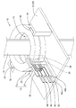
図1〜図4に示すように、本実施形態に係る電流センサ10は、磁性材料により形成された磁性体コア12を備えている。磁性体コア12は、その全体の形状が略円形状でかつ略「C」字状に形成されており、電流経路となる金属製のバスバー14の周囲を取り囲むようにして配置されている(図1参照)。言い換えると、バスバー14は、略C字状に形成された磁性体コア12の中心部13に挿通されている。このバスバー14が、本発明の「導体」に対応している。なお、図2〜図4では、バスバー14を省略している。
Hereinafter, embodiments of the present invention will be described in detail with reference to the drawings.
As illustrated in FIGS. 1 to 4, the
磁性体コア12は、第1コア16及び第2コア18によって構成されている。第1コア16及び第2コア18は、互いに磁気特性の異なる磁性材料によってほぼ同一形状に形成されている。
The
第1コア16及び第2コア18には、それぞれ、所定の大きさのギャップ20、22が形成されている。第1コア16及び第2コア18は、それらのギャップ20、22の位置が一致するようにして、重ねられた状態で一体化されている。
The
第1コア16のギャップ20中には、第1磁電変換素子24が配置されている。一方、第2コア18のギャップ22中には、第2磁電変換素子26が配置されている。第1磁電変換素子24及び第2磁電変換素子26は、例えばホール素子などの磁界の強さを電圧信号に変換することのできる素子によって構成されている。
A first
バスバー14に電流が流れることで発生した磁束は、第1コア16及び第2コア18に集束されるとともに、第1コア16及び第2コア18のギャップ20、22中には、磁界が発生する。
The magnetic flux generated by the current flowing through the
したがって、第1コア16のギャップ20中の磁界の強さを第1磁電変換素子24によって電圧信号に変換することによって、バスバー14に流れる電流の大きさを検出することが可能である。また、第2コア18のギャップ22中の磁界の強さを第2磁電変換素子26によって電圧信号に変換することによって、バスバー14に流れる電流の大きさを検出することが可能である。
Therefore, the magnitude of the current flowing through the
第1コア16は、例えばパーマロイなどの透磁率の高い磁性材料によって形成されている。一方、第2コア18は、例えば純鉄や珪素鋼材といった第1コア16の材料よりも透磁率が低いが飽和磁束密度 (Bs)が大きい磁性材料によって形成されている。
The
第1コア16及び第2コア18は、板状の磁性材料を例えばプレス機によって略C字状に打ち抜くことによって製造することが可能である。あるいは、粉末状の磁性材料を成形型内で圧縮成形したり、粉末状の磁性材料を成形型内で圧縮した後に焼結することによって製造することが可能である。
The
第1コア16及び第2コア18の間には、非磁性材料からなる非磁性層28が介在している。非磁性層28は、比透磁率が1もしくは1に近い非磁性材料、例えば銅などによって形成されている。第1コア16及び第2コア18は、それらの間に非磁性層28を介在させた状態で接着剤などによって積層一体化されている。
A
図1〜図4に示すように、電流センサ10は、磁性体コア12をその内部に収容する合成樹脂製のケース30を備えている。ケース30は、磁性体コア12がその上面側に取り付けられる底板部32と、底板部32の上面側に取り付けられた磁性体コア12の上方に被せられる図示しないキャップ部を備えている。底板部32には、バスバー14を挿通させるための略円形の挿通孔33が設けられている。
As shown in FIGS. 1 to 4, the
ケース30の底板部32の上面には、2本の柱状の固定部34が立設されている。一方、磁性体コア12の側面には、互いに180度離れた位置に2つの固定用リブ36が一体的に設けられている。固定用リブ36を固定部34の内面側に設けられた断面略コの字型の固定溝38に対して上方から嵌合させることによって、底板部32の上面側に磁性体コア12を回転不能な状態で固定することが可能となっている。
Two
また、ケース30の底板部32の上面には、略L字形状の板状部材からなる一対の基板固定部40a、40bが立設されている。一対の基板固定部40a、40bの間には、上記した第1磁電変換素子24及び第2磁電変換素子26が搭載されている基板42が上方から差し込まれて固定されている。
In addition, a pair of
図2に示すように、基板42には、上方から順番に、電源端子44、接地端子46、第1出力端子48、及び第2出力端子50が設けられている。電源端子44及び接地端子46は、それぞれ、基板42の表面に形成された回路を介して第1磁電変換素子24及び第2磁電変換素子26に電気的に接続されている。第1出力端子48は、基板42の表面に形成された回路を介して第1磁電変換素子24に電気的に接続されている。第2出力端子50は、基板42の表面に形成された回路を介して第2磁電変換素子26に電気的に接続されている。
As shown in FIG. 2, the
第1磁電変換素子24において発生した電圧信号は、基板42に搭載された増幅回路によって増幅された後に、第1出力端子48に出力される。第2磁電変換素子26において発生した電圧信号は、基板42に搭載された増幅回路によって増幅された後に、第2出力端子50に出力される。また、電源端子44には、第1磁電変換素子24及び第2磁電変換素子26に対して電気を供給する図示しない電源配線が接続される。接地端子46には、図示しない接地配線が接続される。
The voltage signal generated in the first
上記のように構成された電流センサ10の作用効果について説明する。
本実施形態の電流センサ10によれば、第1コア16及び第2コア18が一体化されているために、第1コア16及び第2コア18をケース30に対して別々に組み付ける必要がない。したがって、第1コア16及び第2コア18をケース30に対して組み付ける作業が容易になる。また2つの磁電変換素子(第1磁電変換素子24及び第2磁電変換素子26)を磁性体コア12に同時に位置合わせ出来るので組立性が向上する。
The effects of the
According to the
本実施形態の電流センサ10によれば、第1コア16及び第2コア18がほぼ同一形状に形成されており、かつ、それらが重ねられた状態で積層一体化されている。したがって、第1コア16及び第2コア18が異なる形状でかつ一体化されていない場合よりも、磁性体コア12を小さくすることが可能である。その結果、電流センサ10をより小型化することが可能である。
According to the
本実施形態の電流センサ10によれば、互いに磁気特性の異なる磁性材料により形成された第1コア16及び第2コア18を備えている。そして、第1コア16は、第2コア18よりも透磁率の高い材料で形成されている。
According to the
この場合、電流値(被測定電流)がある基準値よりも小さい場合には、第1コア16によって電流値を検出することが可能であり、電流値(被測定電流)がある基準値よりも大きい場合には、第2コア18によって電流値を検出することが可能である。これにより、バスバー14に流れる電流の大きさをより広範囲にかつ精密に検出することが可能になる。
In this case, when the current value (current to be measured) is smaller than a certain reference value, the current value can be detected by the
すなわち、透磁率の高い材料で形成されている第1コア16は、電流値が小さい(磁界強度が弱い)場合であっても生じる磁束が多いので、電流値の検出感度が高く、電流値の小さい領域での使用に適しているが、磁気飽和しやすい。一方、透磁率の低い材料で形成されている第2コア18は、電流値の検出感度は第1コア16よりも若干劣るものの、電流値が大きい場合であっても磁気飽和しにくいために、電流値の大きい領域での使用に適している。したがって、第1コア16及び第2コア18を電流値の大きさに応じて適切に使い分けることによって、バスバー14に流れる電流の大きさをより広範囲にかつ精密に検出することが可能になる。
That is, since the
このような第1コア16及び第2コア18の使い分けを実現するために、例えば、電流値(被測定電流)がある基準値よりも小さい場合には、第1出力端子48から出力される電圧信号のみを電流値を検出するための電圧信号として採用し、電流値(被測定電流)がある基準値よりも大きい場合には、第2出力端子50から出力される電圧信号のみを電流値を検出するための電圧信号として採用することのできる制御回路を電流センサ10に搭載してもよい。
In order to realize such proper use of the
本実施形態の電流センサ10によれば、第1コア16及び第2コア18の間に非磁性材料からなる非磁性層28が介在しているために、第1コア16及び第2コア18を磁気的に分離することが可能である。したがって、第1コア16及び第2コア18が磁束の漏れによって互いに干渉し合うことを防止することが可能であり、バスバー14に流れる電流の大きさをより精密に検出することが可能となる。
According to the
<他の実施形態>
本発明は上記記述及び図面によって説明した実施形態に限定されるものではなく、例えば次のような実施形態も本発明の技術的範囲に含まれ、さらに、下記以外にも要旨を逸脱しない範囲内で種々変更して実施することができる。
(1)上記実施形態では、電流センサ10によってバスバー14に流れる被測定電流の電流値を検出する例を示したが、バスバー14以外の導体に流れる被測定電流の電流値を検出する場合であっても本発明を適用することが可能である。例えば、電線に流れる被測定電流の電流値を検出する場合であっても本発明を適用することが可能である。
(2)上記実施形態では、磁性体コア12が略円形状に形成されている例を示したが、磁性体コア12が略矩形状に形成されている場合であっても本発明を適用することが可能である。
(3)上記実施形態では、第1コア16及び第2コア18の間に非磁性層28が介在している例を示したが、第1コア16及び第2コア18の間に非磁性層28が介在していない場合であっても本発明を適用することが可能である。
(4)図5、図6に示すように、磁性体コア12を固定するための固定用リブ36は、180°離れたところだけに設けるのではなく、非対称の位置に設けてもよい。例えば、非対称の位置にリブ36aを設け、第1コア16をリブ36aによって固定するとともに、第2コア18をリブ36によって固定してもよい。
<Other embodiments>
The present invention is not limited to the embodiments described with reference to the above description and drawings. For example, the following embodiments are also included in the technical scope of the present invention, and further, within the scope not departing from the gist of the invention other than the following. Various modifications can be made.
(1) In the above embodiment, the
(2) In the above embodiment, an example in which the
(3) In the above embodiment, the
(4) As shown in FIGS. 5 and 6, the fixing
10・・・電流センサ
12・・・磁性体コア
14・・・バスバー(導体)
16・・・第1コア
18・・・第2コア
20、22・・・ギャップ
24・・・第1磁電変換素子
26・・・第2磁電変換素子
28・・・非磁性層
10 ...
16 ...
Claims (3)
前記磁性体コアは、互いに磁気特性の異なる磁性材料で形成された第1コア及び第2コアからなり、前記第1コア及び前記2コアにはそれぞれギャップが形成されており、前記第1コア及び前記第2コアに形成されたギャップ中にはそれぞれ磁電変換素子が配置されており、
前記第1コア及び前記第2コアは、ほぼ同一形状に形成されており、かつ、それらのギャップの位置が一致するようにして重ねられた状態で一体化されていることを特徴とする電流センサ。 A current sensor for detecting a magnitude of a current flowing in a conductor inserted through the magnetic core by a magnetoelectric transducer disposed in a gap of the magnetic core;
The magnetic core includes a first core and a second core made of magnetic materials having different magnetic characteristics, and a gap is formed in each of the first core and the second core. Magnetoelectric transducers are respectively disposed in the gaps formed in the second core,
The first core and the second core are formed in substantially the same shape, and are integrated in a state of being overlapped so that the positions of the gaps coincide with each other. .
Priority Applications (1)
| Application Number | Priority Date | Filing Date | Title |
|---|---|---|---|
| JP2009279415A JP5516947B2 (en) | 2009-12-09 | 2009-12-09 | Current sensor |
Applications Claiming Priority (1)
| Application Number | Priority Date | Filing Date | Title |
|---|---|---|---|
| JP2009279415A JP5516947B2 (en) | 2009-12-09 | 2009-12-09 | Current sensor |
Publications (2)
| Publication Number | Publication Date |
|---|---|
| JP2011122880A JP2011122880A (en) | 2011-06-23 |
| JP5516947B2 true JP5516947B2 (en) | 2014-06-11 |
Family
ID=44286918
Family Applications (1)
| Application Number | Title | Priority Date | Filing Date |
|---|---|---|---|
| JP2009279415A Expired - Fee Related JP5516947B2 (en) | 2009-12-09 | 2009-12-09 | Current sensor |
Country Status (1)
| Country | Link |
|---|---|
| JP (1) | JP5516947B2 (en) |
Families Citing this family (7)
| Publication number | Priority date | Publication date | Assignee | Title |
|---|---|---|---|---|
| EP2660611A1 (en) * | 2012-04-30 | 2013-11-06 | LEM Intellectual Property SA | Electrical current transducer module |
| JP2014120559A (en) * | 2012-12-14 | 2014-06-30 | Kitagawa Kogyo Co Ltd | Magnetic material core |
| JP6188399B2 (en) * | 2013-04-24 | 2017-08-30 | 日置電機株式会社 | Current sensor |
| KR101715792B1 (en) * | 2014-11-03 | 2017-03-22 | (주)한국센서 | current sensor using multilayered magnetic core |
| JP2016109601A (en) * | 2014-12-09 | 2016-06-20 | 株式会社東海理化電機製作所 | Current sensor |
| JP6526553B2 (en) * | 2015-04-23 | 2019-06-05 | 日立化成株式会社 | Core hold unit for current sensor and method of manufacturing the same |
| JP6914395B1 (en) * | 2020-04-23 | 2021-08-04 | 三菱電機株式会社 | Power converter |
-
2009
- 2009-12-09 JP JP2009279415A patent/JP5516947B2/en not_active Expired - Fee Related
Also Published As
| Publication number | Publication date |
|---|---|
| JP2011122880A (en) | 2011-06-23 |
Similar Documents
| Publication | Publication Date | Title |
|---|---|---|
| JP5516947B2 (en) | Current sensor | |
| JP5524540B2 (en) | Current sensor | |
| CN102749491B (en) | There is the current sensor of magnetic core | |
| JP5879595B2 (en) | Current sensor | |
| JP6131588B2 (en) | Current sensor | |
| WO2013008462A1 (en) | Current sensor substrate and current sensor | |
| JP2008151743A (en) | Current sensor and method for forming the same | |
| JP2013539038A (en) | Battery current sensor | |
| JP2009270910A (en) | Electrical current detector | |
| WO2013175865A1 (en) | Current sensor | |
| JP4645520B2 (en) | Rotation angle detector | |
| JP2010112936A (en) | Current sensor and magnetic detection method | |
| JP2008145352A (en) | Current sensor and current detecting method | |
| JP5666324B2 (en) | Current sensor | |
| JP2011112559A (en) | Current sensor | |
| WO2016093059A1 (en) | Current sensor | |
| WO2014045559A1 (en) | Current sensor | |
| JP2012037377A (en) | Current sensor | |
| JP5086169B2 (en) | Current sensor and method of manufacturing current sensor | |
| JP2014185935A (en) | Current sensor | |
| WO2016021383A1 (en) | Current sensor | |
| JP5666192B2 (en) | Current sensor | |
| JP4459011B2 (en) | Current sensor | |
| CN203084058U (en) | Split type hall current sensor | |
| JP2012163401A (en) | Current sensor |
Legal Events
| Date | Code | Title | Description |
|---|---|---|---|
| A621 | Written request for application examination |
Free format text: JAPANESE INTERMEDIATE CODE: A621 Effective date: 20121015 |
|
| A977 | Report on retrieval |
Free format text: JAPANESE INTERMEDIATE CODE: A971007 Effective date: 20131205 |
|
| A131 | Notification of reasons for refusal |
Free format text: JAPANESE INTERMEDIATE CODE: A131 Effective date: 20131210 |
|
| TRDD | Decision of grant or rejection written | ||
| A01 | Written decision to grant a patent or to grant a registration (utility model) |
Free format text: JAPANESE INTERMEDIATE CODE: A01 Effective date: 20140306 |
|
| A61 | First payment of annual fees (during grant procedure) |
Free format text: JAPANESE INTERMEDIATE CODE: A61 Effective date: 20140319 |
|
| R150 | Certificate of patent or registration of utility model |
Ref document number: 5516947 Country of ref document: JP Free format text: JAPANESE INTERMEDIATE CODE: R150 |
|
| LAPS | Cancellation because of no payment of annual fees |