JP5486610B2 - Fabrication of gallium nitride devices with diamond layers - Google Patents
Fabrication of gallium nitride devices with diamond layers Download PDFInfo
- Publication number
- JP5486610B2 JP5486610B2 JP2011542361A JP2011542361A JP5486610B2 JP 5486610 B2 JP5486610 B2 JP 5486610B2 JP 2011542361 A JP2011542361 A JP 2011542361A JP 2011542361 A JP2011542361 A JP 2011542361A JP 5486610 B2 JP5486610 B2 JP 5486610B2
- Authority
- JP
- Japan
- Prior art keywords
- gan
- layer
- diamond
- diamond layer
- depositing
- Prior art date
- Legal status (The legal status is an assumption and is not a legal conclusion. Google has not performed a legal analysis and makes no representation as to the accuracy of the status listed.)
- Active
Links
- 239000010432 diamond Substances 0.000 title claims description 163
- 229910003460 diamond Inorganic materials 0.000 title claims description 162
- JMASRVWKEDWRBT-UHFFFAOYSA-N Gallium nitride Chemical compound [Ga]#N JMASRVWKEDWRBT-UHFFFAOYSA-N 0.000 title claims description 126
- 229910002601 GaN Inorganic materials 0.000 title claims description 109
- 238000004519 manufacturing process Methods 0.000 title claims description 10
- 238000000034 method Methods 0.000 claims description 81
- XUIMIQQOPSSXEZ-UHFFFAOYSA-N Silicon Chemical compound [Si] XUIMIQQOPSSXEZ-UHFFFAOYSA-N 0.000 claims description 25
- 238000000151 deposition Methods 0.000 claims description 24
- 239000010703 silicon Substances 0.000 claims description 22
- 229910052710 silicon Inorganic materials 0.000 claims description 20
- 239000000758 substrate Substances 0.000 claims description 18
- 239000000463 material Substances 0.000 claims description 14
- HBMJWWWQQXIZIP-UHFFFAOYSA-N silicon carbide Chemical compound [Si+]#[C-] HBMJWWWQQXIZIP-UHFFFAOYSA-N 0.000 claims description 10
- 229910010271 silicon carbide Inorganic materials 0.000 claims description 10
- 238000005229 chemical vapour deposition Methods 0.000 claims description 5
- 239000002245 particle Substances 0.000 claims description 4
- 239000002113 nanodiamond Substances 0.000 claims description 3
- QVGXLLKOCUKJST-UHFFFAOYSA-N atomic oxygen Chemical compound [O] QVGXLLKOCUKJST-UHFFFAOYSA-N 0.000 claims description 2
- 239000011521 glass Substances 0.000 claims description 2
- 229910052760 oxygen Inorganic materials 0.000 claims description 2
- 239000001301 oxygen Substances 0.000 claims description 2
- 229910052594 sapphire Inorganic materials 0.000 claims description 2
- 239000010980 sapphire Substances 0.000 claims description 2
- 238000002604 ultrasonography Methods 0.000 claims description 2
- 238000004050 hot filament vapor deposition Methods 0.000 description 11
- 238000005268 plasma chemical vapour deposition Methods 0.000 description 7
- KFZMGEQAYNKOFK-UHFFFAOYSA-N Isopropanol Chemical compound CC(C)O KFZMGEQAYNKOFK-UHFFFAOYSA-N 0.000 description 6
- 238000010586 diagram Methods 0.000 description 6
- 238000005530 etching Methods 0.000 description 6
- 230000008021 deposition Effects 0.000 description 5
- 229910052581 Si3N4 Inorganic materials 0.000 description 4
- VYPSYNLAJGMNEJ-UHFFFAOYSA-N Silicium dioxide Chemical compound O=[Si]=O VYPSYNLAJGMNEJ-UHFFFAOYSA-N 0.000 description 4
- 239000000853 adhesive Substances 0.000 description 4
- 230000001070 adhesive effect Effects 0.000 description 4
- 229910002704 AlGaN Inorganic materials 0.000 description 3
- 239000011248 coating agent Substances 0.000 description 3
- 238000000576 coating method Methods 0.000 description 3
- 238000009792 diffusion process Methods 0.000 description 3
- 239000012212 insulator Substances 0.000 description 2
- 238000001465 metallisation Methods 0.000 description 2
- 235000012239 silicon dioxide Nutrition 0.000 description 2
- 239000000377 silicon dioxide Substances 0.000 description 2
- HQVNEWCFYHHQES-UHFFFAOYSA-N silicon nitride Chemical compound N12[Si]34N5[Si]62N3[Si]51N64 HQVNEWCFYHHQES-UHFFFAOYSA-N 0.000 description 2
- 239000003990 capacitor Substances 0.000 description 1
- 230000000694 effects Effects 0.000 description 1
- 229920002120 photoresistant polymer Polymers 0.000 description 1
- 230000000704 physical effect Effects 0.000 description 1
- WFKWXMTUELFFGS-UHFFFAOYSA-N tungsten Chemical compound [W] WFKWXMTUELFFGS-UHFFFAOYSA-N 0.000 description 1
- 229910052721 tungsten Inorganic materials 0.000 description 1
- 239000010937 tungsten Substances 0.000 description 1
Images


Classifications
-
- H—ELECTRICITY
- H01—ELECTRIC ELEMENTS
- H01L—SEMICONDUCTOR DEVICES NOT COVERED BY CLASS H10
- H01L29/00—Semiconductor devices adapted for rectifying, amplifying, oscillating or switching, or capacitors or resistors with at least one potential-jump barrier or surface barrier, e.g. PN junction depletion layer or carrier concentration layer; Details of semiconductor bodies or of electrodes thereof ; Multistep manufacturing processes therefor
- H01L29/66—Types of semiconductor device ; Multistep manufacturing processes therefor
- H01L29/68—Types of semiconductor device ; Multistep manufacturing processes therefor controllable by only the electric current supplied, or only the electric potential applied, to an electrode which does not carry the current to be rectified, amplified or switched
- H01L29/76—Unipolar devices, e.g. field effect transistors
- H01L29/772—Field effect transistors
- H01L29/778—Field effect transistors with two-dimensional charge carrier gas channel, e.g. HEMT ; with two-dimensional charge-carrier layer formed at a heterojunction interface
- H01L29/7786—Field effect transistors with two-dimensional charge carrier gas channel, e.g. HEMT ; with two-dimensional charge-carrier layer formed at a heterojunction interface with direct single heterostructure, i.e. with wide bandgap layer formed on top of active layer, e.g. direct single heterostructure MIS-like HEMT
-
- H—ELECTRICITY
- H01—ELECTRIC ELEMENTS
- H01L—SEMICONDUCTOR DEVICES NOT COVERED BY CLASS H10
- H01L21/00—Processes or apparatus adapted for the manufacture or treatment of semiconductor or solid state devices or of parts thereof
- H01L21/02—Manufacture or treatment of semiconductor devices or of parts thereof
- H01L21/04—Manufacture or treatment of semiconductor devices or of parts thereof the devices having at least one potential-jump barrier or surface barrier, e.g. PN junction, depletion layer or carrier concentration layer
- H01L21/18—Manufacture or treatment of semiconductor devices or of parts thereof the devices having at least one potential-jump barrier or surface barrier, e.g. PN junction, depletion layer or carrier concentration layer the devices having semiconductor bodies comprising elements of Group IV of the Periodic System or AIIIBV compounds with or without impurities, e.g. doping materials
-
- H—ELECTRICITY
- H01—ELECTRIC ELEMENTS
- H01L—SEMICONDUCTOR DEVICES NOT COVERED BY CLASS H10
- H01L21/00—Processes or apparatus adapted for the manufacture or treatment of semiconductor or solid state devices or of parts thereof
- H01L21/02—Manufacture or treatment of semiconductor devices or of parts thereof
- H01L21/02104—Forming layers
- H01L21/02365—Forming inorganic semiconducting materials on a substrate
- H01L21/02367—Substrates
- H01L21/0237—Materials
- H01L21/02387—Group 13/15 materials
- H01L21/02389—Nitrides
-
- H—ELECTRICITY
- H01—ELECTRIC ELEMENTS
- H01L—SEMICONDUCTOR DEVICES NOT COVERED BY CLASS H10
- H01L21/00—Processes or apparatus adapted for the manufacture or treatment of semiconductor or solid state devices or of parts thereof
- H01L21/02—Manufacture or treatment of semiconductor devices or of parts thereof
- H01L21/02104—Forming layers
- H01L21/02365—Forming inorganic semiconducting materials on a substrate
- H01L21/02518—Deposited layers
- H01L21/02521—Materials
- H01L21/02524—Group 14 semiconducting materials
- H01L21/02527—Carbon, e.g. diamond-like carbon
-
- H—ELECTRICITY
- H01—ELECTRIC ELEMENTS
- H01L—SEMICONDUCTOR DEVICES NOT COVERED BY CLASS H10
- H01L21/00—Processes or apparatus adapted for the manufacture or treatment of semiconductor or solid state devices or of parts thereof
- H01L21/02—Manufacture or treatment of semiconductor devices or of parts thereof
- H01L21/02104—Forming layers
- H01L21/02365—Forming inorganic semiconducting materials on a substrate
- H01L21/02612—Formation types
- H01L21/02617—Deposition types
- H01L21/0262—Reduction or decomposition of gaseous compounds, e.g. CVD
-
- H—ELECTRICITY
- H01—ELECTRIC ELEMENTS
- H01L—SEMICONDUCTOR DEVICES NOT COVERED BY CLASS H10
- H01L29/00—Semiconductor devices adapted for rectifying, amplifying, oscillating or switching, or capacitors or resistors with at least one potential-jump barrier or surface barrier, e.g. PN junction depletion layer or carrier concentration layer; Details of semiconductor bodies or of electrodes thereof ; Multistep manufacturing processes therefor
- H01L29/02—Semiconductor bodies ; Multistep manufacturing processes therefor
- H01L29/12—Semiconductor bodies ; Multistep manufacturing processes therefor characterised by the materials of which they are formed
- H01L29/16—Semiconductor bodies ; Multistep manufacturing processes therefor characterised by the materials of which they are formed including, apart from doping materials or other impurities, only elements of Group IV of the Periodic System
- H01L29/1602—Diamond
-
- H—ELECTRICITY
- H01—ELECTRIC ELEMENTS
- H01L—SEMICONDUCTOR DEVICES NOT COVERED BY CLASS H10
- H01L29/00—Semiconductor devices adapted for rectifying, amplifying, oscillating or switching, or capacitors or resistors with at least one potential-jump barrier or surface barrier, e.g. PN junction depletion layer or carrier concentration layer; Details of semiconductor bodies or of electrodes thereof ; Multistep manufacturing processes therefor
- H01L29/02—Semiconductor bodies ; Multistep manufacturing processes therefor
- H01L29/12—Semiconductor bodies ; Multistep manufacturing processes therefor characterised by the materials of which they are formed
- H01L29/26—Semiconductor bodies ; Multistep manufacturing processes therefor characterised by the materials of which they are formed including, apart from doping materials or other impurities, elements provided for in two or more of the groups H01L29/16, H01L29/18, H01L29/20, H01L29/22, H01L29/24, e.g. alloys
- H01L29/267—Semiconductor bodies ; Multistep manufacturing processes therefor characterised by the materials of which they are formed including, apart from doping materials or other impurities, elements provided for in two or more of the groups H01L29/16, H01L29/18, H01L29/20, H01L29/22, H01L29/24, e.g. alloys in different semiconductor regions, e.g. heterojunctions
-
- H—ELECTRICITY
- H01—ELECTRIC ELEMENTS
- H01L—SEMICONDUCTOR DEVICES NOT COVERED BY CLASS H10
- H01L29/00—Semiconductor devices adapted for rectifying, amplifying, oscillating or switching, or capacitors or resistors with at least one potential-jump barrier or surface barrier, e.g. PN junction depletion layer or carrier concentration layer; Details of semiconductor bodies or of electrodes thereof ; Multistep manufacturing processes therefor
- H01L29/66—Types of semiconductor device ; Multistep manufacturing processes therefor
- H01L29/66007—Multistep manufacturing processes
- H01L29/66075—Multistep manufacturing processes of devices having semiconductor bodies comprising group 14 or group 13/15 materials
- H01L29/66227—Multistep manufacturing processes of devices having semiconductor bodies comprising group 14 or group 13/15 materials the devices being controllable only by the electric current supplied or the electric potential applied, to an electrode which does not carry the current to be rectified, amplified or switched, e.g. three-terminal devices
- H01L29/66409—Unipolar field-effect transistors
- H01L29/66431—Unipolar field-effect transistors with a heterojunction interface channel or gate, e.g. HFET, HIGFET, SISFET, HJFET, HEMT
-
- H—ELECTRICITY
- H01—ELECTRIC ELEMENTS
- H01L—SEMICONDUCTOR DEVICES NOT COVERED BY CLASS H10
- H01L29/00—Semiconductor devices adapted for rectifying, amplifying, oscillating or switching, or capacitors or resistors with at least one potential-jump barrier or surface barrier, e.g. PN junction depletion layer or carrier concentration layer; Details of semiconductor bodies or of electrodes thereof ; Multistep manufacturing processes therefor
- H01L29/66—Types of semiconductor device ; Multistep manufacturing processes therefor
- H01L29/66007—Multistep manufacturing processes
- H01L29/66075—Multistep manufacturing processes of devices having semiconductor bodies comprising group 14 or group 13/15 materials
- H01L29/66227—Multistep manufacturing processes of devices having semiconductor bodies comprising group 14 or group 13/15 materials the devices being controllable only by the electric current supplied or the electric potential applied, to an electrode which does not carry the current to be rectified, amplified or switched, e.g. three-terminal devices
- H01L29/66409—Unipolar field-effect transistors
- H01L29/66446—Unipolar field-effect transistors with an active layer made of a group 13/15 material, e.g. group 13/15 velocity modulation transistor [VMT], group 13/15 negative resistance FET [NERFET]
- H01L29/66462—Unipolar field-effect transistors with an active layer made of a group 13/15 material, e.g. group 13/15 velocity modulation transistor [VMT], group 13/15 negative resistance FET [NERFET] with a heterojunction interface channel or gate, e.g. HFET, HIGFET, SISFET, HJFET, HEMT
-
- H—ELECTRICITY
- H01—ELECTRIC ELEMENTS
- H01L—SEMICONDUCTOR DEVICES NOT COVERED BY CLASS H10
- H01L29/00—Semiconductor devices adapted for rectifying, amplifying, oscillating or switching, or capacitors or resistors with at least one potential-jump barrier or surface barrier, e.g. PN junction depletion layer or carrier concentration layer; Details of semiconductor bodies or of electrodes thereof ; Multistep manufacturing processes therefor
- H01L29/66—Types of semiconductor device ; Multistep manufacturing processes therefor
- H01L29/68—Types of semiconductor device ; Multistep manufacturing processes therefor controllable by only the electric current supplied, or only the electric potential applied, to an electrode which does not carry the current to be rectified, amplified or switched
- H01L29/76—Unipolar devices, e.g. field effect transistors
- H01L29/772—Field effect transistors
- H01L29/778—Field effect transistors with two-dimensional charge carrier gas channel, e.g. HEMT ; with two-dimensional charge-carrier layer formed at a heterojunction interface
-
- H—ELECTRICITY
- H01—ELECTRIC ELEMENTS
- H01L—SEMICONDUCTOR DEVICES NOT COVERED BY CLASS H10
- H01L29/00—Semiconductor devices adapted for rectifying, amplifying, oscillating or switching, or capacitors or resistors with at least one potential-jump barrier or surface barrier, e.g. PN junction depletion layer or carrier concentration layer; Details of semiconductor bodies or of electrodes thereof ; Multistep manufacturing processes therefor
- H01L29/02—Semiconductor bodies ; Multistep manufacturing processes therefor
- H01L29/12—Semiconductor bodies ; Multistep manufacturing processes therefor characterised by the materials of which they are formed
- H01L29/20—Semiconductor bodies ; Multistep manufacturing processes therefor characterised by the materials of which they are formed including, apart from doping materials or other impurities, only AIIIBV compounds
- H01L29/2003—Nitride compounds
Description
窒化ガリウム(GaN)は、その電気的および物理的特性のために、マイクロ波デバイスのような高周波(HF)デバイスに非常に適するものになっている。HFデバイスは、大量の熱を発生するので、デバイスの障害を回避するために、当該HFデバイスに熱拡散部(heat spreader)を付着させる必要がある。このような熱拡散部の1つにダイアモンドがある。GaN層上で用いられるダイアモンドを形成するために、ホット・フィラメント化学蒸着(CVD:chemical vapor deposition)プロセスが用いられている。一般に、これらのダイアモンド層は直接GaN層上に堆積されるのではなく、何らかの他の材料(例えば、シリコン、シリコン・カーバイド等)の上に堆積され、この材料が最終的にGaN層と共に処理される。 Gallium nitride (GaN) has become very suitable for high frequency (HF) devices such as microwave devices because of its electrical and physical properties. Since an HF device generates a large amount of heat, it is necessary to attach a heat spreader to the HF device in order to avoid failure of the device. One such thermal diffusion section is diamond. A hot filament chemical vapor deposition (CVD) process has been used to form the diamond used on the GaN layer. In general, these diamond layers are not deposited directly on the GaN layer, but are deposited on some other material (eg, silicon, silicon carbide, etc.) and this material is finally processed with the GaN layer. The
一態様における方法は、デバイスを製造するステップを含む。このデバイスは、窒化ガリウム(GaN)層と、この窒化ガリウム層上に配置されたダイアモンド層と、GaN層およびダイアモンド層と接触して配置されたゲート構造とを含む。 The method in one aspect includes manufacturing a device. The device includes a gallium nitride (GaN) layer, a diamond layer disposed on the gallium nitride layer, and a gate structure disposed in contact with the GaN layer and the diamond layer.
他の態様におけるデバイスは、窒化ガリウム(GaN)層と、GaN層上に配置されたダイアモンド層と、GaN層およびダイアモンド層と接触して配置されたゲート構造とを含む。 A device in another aspect includes a gallium nitride (GaN) layer, a diamond layer disposed on the GaN layer, and a gate structure disposed in contact with the GaN layer and the diamond layer.
更に別の態様における方法は、窒化ガリウム(GaN)の第1表面上にダイアモンド層を配置するステップと、ダイアモンド層の一部を除去して、GaNの第1表面を露出させるステップと、GaNの第1表面およびダイアモンド層に接触するゲート構造を形成するステップとを含む。 In yet another aspect, a method includes disposing a diamond layer on a first surface of gallium nitride (GaN), removing a portion of the diamond layer to expose the first surface of GaN, Forming a gate structure in contact with the first surface and the diamond layer.
ホット・フィラメント化学蒸着(CVD)プロセスは、窒化ガリウム(GaN)層上で用いられる1ミル未満のダイアモンド層を形成するために用いられてきた。熱拡散部として有効であるためには、ダイアモンド層は2ミルよりも大きくなければならない。更に、ホット・フィラメントCVDプロセスは、それ自体の本質により、黒っぽい色のダイアモンドを生成する。これは、例えば、タングステンのような、ホット・フィラメントCVDプロセスにおいて用いられる材料が混入されたためである。一般に、これらの「汚れた」ダイアモンド層が生成されると、純粋なダイアモンドよりも熱伝導率が低くなる。一般に、ホット・フィラメントCVDプロセスを用いたダイアモンド層の熱伝導率は、約800から1000ワット/メートル−ケルビン(W/m−K)である。 Hot filament chemical vapor deposition (CVD) processes have been used to form sub-mil diamond layers used on gallium nitride (GaN) layers. In order to be effective as a heat spreader, the diamond layer must be greater than 2 mils. Furthermore, the hot filament CVD process, due to its own nature, produces dark diamonds. This is because a material used in the hot filament CVD process, such as tungsten, is mixed in. In general, when these “dirty” diamond layers are produced, they have a lower thermal conductivity than pure diamond. Generally, the thermal conductivity of a diamond layer using a hot filament CVD process is about 800 to 1000 Watts / meter-Kelvin (W / m-K).
マイクロ波プラズマCVDプロセスは、ホット・フィラメントCVDプロセスよりも遙かに厚い4ミルのオーダーのダイアモンド層を、遙かに速い速度で生産することが知られている。更に、このダイアモンド層は、ホット・フィラメントCVDプロセスよりも純粋であり、1500W/m−Kよりも大きな熱伝導率を有するダイアモンド層を生産する。一例では、マイクロ波プラズマCVDプロセスを用いて生産されたダイアモンドの熱伝導率は、ホット・フィラメント・プロセスを用いて生産されたダイアモンドの熱伝導率の2倍となる。しかしながら、マイクロ波プラズマDVDプロセスを含むCVDプロセスは、GaN上への直接堆積に関しては比較的知られていない。例えば、ホット・フィラメントCVDを用いたダイアモンドの堆積は、通例、何らかの他の材料(例えば、シリコン、シリコン・カーバイド等)の上に行われ、この他の材料が最終的にGaN層と共に処理される。マイクロ波プラズマCVDプロセスを用いたGaN上へのダイアモンドの直接堆積は比較的知られていないので、GaN上に直接ダイアモンドを堆積させるためのプロセスを信頼性高くそして首尾良く開発し検査するコストは非常に高くなる。GaN上に直接ダイアモンドを堆積させるプロセスを開発するコストや出費を迂回する1つの方法は、マイクロ波プラズマCVDプロセスを用いたダイアモンドを、例えば、ホット・フィラメントCVDを用いて製造された劣等ダイアモンド層(inferior diamond layer)上に堆積させることである。 Microwave plasma CVD processes are known to produce diamond layers on the order of 4 mils that are much thicker than hot filament CVD processes at much faster rates. Furthermore, this diamond layer is purer than the hot filament CVD process and produces a diamond layer with a thermal conductivity greater than 1500 W / m-K. In one example, the thermal conductivity of a diamond produced using a microwave plasma CVD process is twice that of a diamond produced using a hot filament process. However, CVD processes including microwave plasma DVD processes are relatively unknown for direct deposition on GaN. For example, diamond deposition using hot filament CVD is typically performed on some other material (eg, silicon, silicon carbide, etc.), which is ultimately processed with the GaN layer. . Since the direct deposition of diamond on GaN using microwave plasma CVD process is relatively unknown, the cost of developing and testing a reliable and successful process for depositing diamond directly on GaN is very high To be high. One way to bypass the cost and expense of developing a process for depositing diamond directly on GaN is to use a diamond using a microwave plasma CVD process, eg, an inferior diamond layer manufactured using hot filament CVD ( inferior diamond layer).
本明細書において用いる場合、GaN層は、純粋のGaN、ドープGaN(doped GaN)、または他の元素と組み合わされたGaN(例えば、AlGaN)、あるいはそのあらゆる組み合わせを含むことができる。シリコン基板は、純粋なシリコン、ドープ・シリコン、二酸化シリコン、シリコン・カーバイド、またはシリコンと他の元素とのあらゆる組み合わせ、ならびにそのあらゆる組み合わせを含むことができる。 As used herein, a GaN layer can include pure GaN, doped GaN, or GaN combined with other elements (eg, AlGaN), or any combination thereof. The silicon substrate can include pure silicon, doped silicon, silicon dioxide, silicon carbide, or any combination of silicon and other elements, as well as any combination thereof.
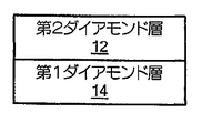
図1Aおよび図1Bを参照すると、一例において、デバイス(例えば、高周波デバイス、高電子移動度トランジスタ(HEMT)、マイクロ波デバイス等)を形成する際に用いるための構造10は、第2ダイアモンド層12、第2ダイアモンド層に隣接する第1ダイアモンド層14、そして第1ダイアモンド層に隣接するGaN層16を含む。この構成では、GaN層16によって生成された熱が、第1および第2ダイアモンド層12、14によって形成された熱拡散部を通過する。他の例では、デバイス(例えば、高周波デバイス、HEMTトランジスタ、マイクロ波デバイス等)を形成するために用いられる構造20は、構造10と同様であるが、第1ダイアモンド層とGaN層16との間に中間層22を含む。この中間層22が必要なのは、GaN上へのダイアモンドの直接製造が容易なプロセスではなく、予測可能性や一貫性が遙かに低いからである。中間層22は、単に第1ダイアモンド層14をGaN層に保持する接着性のあるものでよく、またはダイアモンドを容易に堆積させることができるシリコン型構造であってもよい。場合によっては、中間層22がダイアモンド層12、14よりも低い熱伝導率を有するために、中間層22がより多くの熱を保持することもある。即ち、別の言い方をすれば、GaN層16からの熱移転が中間層22によって妨げられることになる。つまり、中間層22を最小に抑えること、または構造10内に中間層を全く有さないことが好ましい。
Referring to FIGS. 1A and 1B, in one example, a
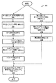
図2および図3Aから図3Dを参照すると、第1ダイアモンド層および第2ダイアモンド層を有するGaN層を製造するプロセスの1つが、プロセス100である。第1ダイアモンド層14(例えば、厚さが5から20ミクロンの層)を絶縁物上シリコン(SOI)基板122(102)(図3A)上に堆積させるために、ホット・フィラメントCVDプロセスが用いられる。絶縁体(図示せず)(例えば、二酸化シリコン)が、SOI基板122から除去されて、シリコン基板122’、例えば、(104)(図3B)を残す。第2ダイアモンド層12を第1ダイアモンド層14(108)(図3C)上に堆積させるために、マイクロ波プラズマCVDが用いられる。残留するSOI基板、つまり、シリコン基板122(112)(図3D)上にGaNを成長させる。
Referring to FIGS. 2 and 3A-3D, one of the processes for producing a GaN layer having a first diamond layer and a second diamond layer is
図4および図5Aから図5Hを参照すると、第1ダイアモンド層および第2ダイアモンド層を有するGaN層を製造する他のプロセスは、プロセス200である。第1基板230(202)(図5A)上に、GaN16を成長させる。一例では、第1基板は、シリコン・カーバイド、シリコン、またはサファイアとするとよい。シリコン層232(例えば、シリコン、シリコン・カーバイド等)を、GaN(204)(図5B)上に堆積させる。一例では、接着剤を用いて、シリコン層232をGaN16に付着させる。他の例では、GaN16上にシリコン層232を成長させる。他の例では、ガラスのような他の材料を、シリコン層232の代わりに用いることもできる。例えば、エッチングによって、第1基板230を除去し(208)、GaN/シリコン構造250(図5C)を残す。ダイアモンドの第1層14を第2基板234(212)(図5D)上に堆積させるために、ホット・フィラメントCVDを用いる。例えば、第2基板234は、厚さが500ミクロンのシリコン基板500である。第1ダイアモンド層14(218)(図5E)上に第2ダイアモンド層12を堆積させるために、マイクロ波プラズマCVDプロセスを用いる。例えば、エッチングによって(図5F)、第2基板234を除去する(218)。第1および第2ダイアモンド層12、14を、GaN/シリコン構造250(224)(図5G)に付着させる。例えば、接着剤を用いて、第1ダイアモンド層14をGaN16に付着させる。例えば、エッチングによって(図5H)、シリコン層232を除去する(228)。
Referring to FIGS. 4 and 5A-5H, another process for producing a GaN layer having a first diamond layer and a second diamond layer is
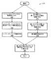
図6および図7Aから図7Fを参照すると、ダイアモンド層を有するGaN層を製造する更に別のプロセスは、プロセス300である。プロセス300は、第3ダイアモンド層316を、第1および第2ダイアモンド層14、12を有する第2GaN面304(例えば、下面)(図7F)とは逆側の第1GaN面302(例えば、上面)(図7F)上に堆積させることを除いて、プロセス200と同様である。例えば、処理ブロック202、204、および208は、プロセス200におけるものと同様に行われる。特には、第1基板230(202)(図7A)上にGaN16を成長させ、GaN16(204)(図7B)上にシリコン層232を堆積させ、例えば、エッチングによって第1基板230を除去し(208)、GaN/シリコン構造250(図7C)を残す。
With reference to FIG. 6 and FIGS. 7A-7F, yet another process for producing a GaN layer having a diamond layer is
シリコン/GaN構造250を溶液中に浸漬して、超音波を付す(302)。堆積(例えば、処理ブロック314)の前に表面を処理することによって、堆積中にダイアモンド層316がGaN16上に形成される可能性(chance)が高くなる。一例では、この溶液は、ダイアモンド粒子(例えば、ナノ−ダイアモンド粒子(10−9m))を含むイソプロピル・アルコール溶液である。
The silicon /
シリコン/GaN構造250(314)(図7D)上に、第3ダイアモンド層316を堆積させる。例えば、約600°Cから約650°Cの温度で、第3ダイアモンド層316をGaN250に堆積させるために、マイクロ波プラズマCVDプロセスを用いる。例えば、エッチング(図7E)によって、シリコン層232を除去する(228)。
A
プロセス・ブロック212、214、および218を用いて形成した第1および第2ダイアモンド層14、12を、残りのGaN/ダイアモンド構造に付着させて、ダイアモンド/GaN/ダイアモンド/ダイアモンド構造360(334)(図7F)を形成する。例えば、接着剤を用いて、第1ダイアモンド層14をGaN16に付着させる。第3ダイアモンド層316が堆積されている第1面302とは逆側の第2面304に、第1ダイアモンド層14を付着させる。ダイアモンド層12、14からは逆側の表面にダイアモンド層316を堆積させることによって、ダイアモンド/GaN/ダイアモンド/ダイアモンド構造360から形成されたデバイスから、熱を一層効果的に排除する。
First and second diamond layers 14, 12 formed using process blocks 212, 214, and 218 are attached to the remaining GaN / diamond structure to form diamond / GaN / diamond / diamond structure 360 (334) ( FIG. 7F) is formed. For example, the
図8および図9Aから図9Dを参照すると、ダイアモンド層を有するGaNを製造する更に別のプロセスは、プロセス370である。シリコン・カーバイド/GaN構造380(図9A)は、GaN層16と、当該GaN16の第2面に堆積されているシリコン・カーバイド層382とを含む。シリコン・カーバイド/GaN構造380を、ナノ−ダイアモンド粒子を有するイソプロピル・アルコール溶液(例えば、処理ブロック312において用いた溶液)に浸漬し、超音波を付す(372)。GaN16(図9B)上に第3ダイアモンド層316を堆積させる(374)。例えば、エッチングによってシリコン・カーバイド層382を除去する(376)(図9C)。例えば、処理ブロック212、214、および218を用いて、第1および第2ダイアモンド層14、12を形成する。第1および第2ダイアモンド層14、12をGaN/ダイアモンド350に付着させて、ダイアモンド/GaN/ダイアモンド/ダイアモンド構造360を形成する(334)(図9D)。
With reference to FIGS. 8 and 9A-9D, yet another process for producing GaN having a diamond layer is
図10を参照すると、高周波デバイス、高電子移動度トランジスタ(HEMT)、マイクロ波デバイス等のようなデバイスを製造するために、ダイアモンド/GaN/ダイアモンド/ダイアモンド構造360を用いることができる。例えば、ダイアモンド層316を直接デバイス内に一体化し、熱を除去するためだけでなく、例えば、容量に用いられる誘電体として機能するために用いることができる。例えば、ダイアモンドの誘電率は約5.7であり、GaNデバイスにおいて広く一般に用いられている窒化シリコンの誘電率である約7に近い。しかしながら、ダイアモンド・フィルムは、窒化シリコン・フィルムよりも熱伝導率が高い。場合によっては、ダイアモンド層316の一部を除去し(例えば、酸素プラズマを用いる)、GaN16の表面302を露出させることもある。
Referring to FIG. 10, a diamond / GaN / diamond /
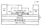
一例では、デバイス400(例えば、HEMTデバイス)は、ソース404、ドレイン406、およびゲート408(例えば、T−ゲート)を含み、これらはメタライゼーション工程において、GaN層16の面302上に堆積される。ゲート408は、ダイアモンド層の一部を除去することによってGaNを露出させた後に、ダイアモンド層316内に形成される。この例では、ダイアモンド層316の一部を除去することによって、ダイアモンド層を、各々幅Wを有する、2つのダイアモンド層316a、316bに分割する。この構成では、ダイアモンド層316a、316bは、誘電体層および熱拡散部として機能することができ、ゲート408から熱を除去する。場合によっては、ダイアモンド層316a、316bの幅が等しくなくてもよい場合もある。一例では、ゲート408の一部がダイアモンド層316a、316bと隣り合ってこれらと接触しており、ゲート408の他の部分が、ゲートとダイアモンド層316a、316bとの間にギャップ410a、410b(例えば、空気ギャップ)を形成する。一例では、ゲート408、ギャップ410a、410b、ダイアモンド層316a、316bが、容量構造を形成する。尚、当業者であれば、これらのギャップ410a、410bを形成するための様々な方法を知っているであろう。例えば、ゲート408を形成するメタライゼーションの前に、ダイアモンド層316の表面に、材料(例えば、フォトレジスト)があってもよい。ゲート408を形成した後、この材料を除去して、ギャップ410a、410bを形成する。他の例では、デバイス400はギャップ410a、410bを含まないので、ゲート408が直接ダイアモンド層316a、316bの表面上にある。更に別の例では、他の材料がギャップ410a、410bを充填してもよい。この材料は、容量に寄与してもしなくてもよい。
In one example, device 400 (eg, a HEMT device) includes a
図11および図12を参照すると、デバイス400’はデバイス400と同様であり、GaN層16が、AlGaN層412および純粋なGaN層416を含む。AlGaN412以外のGaN型材料をGaN層416に追加してもよい。また、GaN層416を、ドープGaNまたは他のGaN型材料と置き換えてもよい。第3ダイアモンド層316a、316bは、熱をゲートから拡散させることによって、ゲート408における温度を大幅に低下させるために用いられる。グラフ500は、デバイス400’を用いた熱の効果を、ダイアモンド層316aまたは316bの幅Wの関数として表す。ゲート408とソース404との間の距離Dは、1.875ミクロンであり、ダイアモンド層316a、316b間の距離Gは、0.25ミクロンである。曲線502は、0.05ミクロンのダイアモンド層を表し、曲線504は、0.25ミクロンのダイアモンド層を表す。0.25ミクロンのダイアモンド・コーティングによって、ダイアモンド層316a、316bを有さない場合よりも、出力電力の20%増大が可能となり、熱抵抗を15%(5W/mmにおいて>25°C)低減できる。0.05ミクロンのダイアモンド・コーティングによって、 ダイアモンド層316a、316bを有さない場合よりも、 熱抵抗を10%(5W/mmにおいて>25°C)低減できる。
Referring to FIGS. 11 and 12,
本明細書において説明したプロセスは、本明細書において説明した特定の実施形態に限定されるのではない。例えば、プロセスは、図2、図4、図6、および図8におけるプロセス工程の特定の処理順序に限定されるのではない。逆に、図2、図4、図6、および図8の処理工程は、そのいずれでも、以上に明記した結果を達成するために必要に応じて、並び替えること、組み合わせるまたは除去すること、並列または直列に実行することができる。 The processes described herein are not limited to the specific embodiments described herein. For example, the process is not limited to the specific processing order of the process steps in FIGS. 2, 4, 6, and 8. Conversely, any of the processing steps of FIGS. 2, 4, 6, and 8 may be reordered, combined or removed, and paralleled as necessary to achieve the results specified above. Or it can be done in series.
以上、一定の構成要素を所与の順序で有する例示的な生産物を有する特定の実施形態と結びつけて本発明について示し説明したが、本発明の範囲内で、構成要素の数がそれよりも多いまたは少ない他の実施形態、異なるタイプの構成要素を有する他の実施形態、そして種々の構成で結合されている実施形態も考えられることは言うまでもない。このような実施形態は、当業者には容易に明らかとなるであろう。本明細書において具体的に記載していない他の実施形態も、以下の特許請求の範囲に該当するものとする。 Although the present invention has been shown and described in connection with a particular embodiment having an exemplary product having certain components in a given order, within the scope of the present invention, the number of components is more than that. It goes without saying that many or fewer other embodiments, other embodiments having different types of components, and embodiments combined in various configurations are also conceivable. Such embodiments will be readily apparent to those skilled in the art. Other embodiments not specifically described in this specification shall fall within the scope of the following claims.
Claims (25)
前記GaN層上に配置された第1ダイアモンド層と、
前記GaN層および前記第1ダイアモンド層と接触して配置されたゲート構造と、
を備えているデバイスを製造するステップを含み、
該製造するステップが、
前記GaN層の第1表面上に第1ダイアモンド層を堆積させること、及び
前記GaN層の第1表面とは反対側となる、前記GaN層の第2表面上に第2ダイアモンド層を堆積させ、且つ、該第2ダイアモンド層に第3ダイアモンド層を堆積させて、前記第2ダイアモンド層および前記第3ダイアモンド層を前記第2表面上に付着させること、を含む、
方法。 A gallium nitride (GaN) layer;
A first diamond layer disposed on the GaN layer;
A gate structure disposed in contact with the GaN layer and the first diamond layer;
Manufacturing a device comprising:
The manufacturing step comprises:
Depositing a first diamond layer on the first surface of the GaN layer, and depositing a second diamond layer on the second surface of the GaN layer opposite to the first surface of the GaN layer ; and, depositing a third diamond layer on the second diamond layer, comprising Rukoto, the depositing the second diamond layer and the third diamond layer on the second surface,
Method.
前記ダイアモンド層の一部を除去して、前記GaNの第1表面を露出させるステップと、
前記GaNの第1表面および前記ダイアモンド層に接触するゲート構造を形成するステップと、
前記GaNの第1表面の反対側となる、前記GaNの第2表面に第2ダイアモンド層を付着させるステップと、
を備えている、方法。 Disposing a diamond layer on a first surface of gallium nitride (GaN);
Removing a portion of the diamond layer to expose the first surface of the GaN;
Forming a gate structure in contact with the first surface of the GaN and the diamond layer;
Depositing a second diamond layer on the second surface of the GaN, opposite the first surface of the GaN;
A method.
第1基板上にGaNを成長させるステップと、
前記GaN上に材料層を堆積させるステップと、
前記第1基板を除去するステップと、
を備えている、方法。 The method of claim 7, comprising:
Growing GaN on the first substrate;
Depositing a material layer on the GaN;
Removing the first substrate;
A method.
前記GaN層上に配置された第1ダイアモンド層と、
前記GaN層および前記第1ダイアモンド層と接触して配置されたゲート構造と、
第1熱伝導率を有し、前記GaN層の第2表面上に堆積された第2ダイアモンド層と、
前記第2ダイアモンド層上に堆積された第3ダイアモンド層と、を備えており、
前記ゲート構造および前記第1ダイアモンド層が、前記GaNの第2表面とは反対側となる、前記GaN層の第1表面上に堆積される、デバイス。 A gallium nitride (GaN) layer;
A first diamond layer disposed on the GaN layer;
A gate structure disposed in contact with the GaN layer and the first diamond layer;
A second diamond layer having a first thermal conductivity and deposited on the second surface of the GaN layer;
A third diamond layer deposited on the second diamond layer ,
The device, wherein the gate structure and the first diamond layer are deposited on a first surface of the GaN layer opposite the second surface of the GaN.
前記GaN層上に配置された第1ダイアモンド層と、
前記GaN層および前記第1ダイアモンド層と接触して配置されたゲート構造と、
第1熱伝導率を有し、前記GaN層の第2表面上に堆積された第2ダイアモンド層と、
前記第2ダイアモンド層と前記GaN層との間に堆積された中間層と、
前記第2ダイアモンド層上に堆積された第3ダイアモンド層と、
を備えており、
前記ゲートおよび前記第1ダイアモンド層が、前記GaNの第2表面とは反対側となる、前記GaN層の第1表面上に堆積され、
前記GaN層が、非ドープGaN、ドープGaN、または他の元素と組み合わせたGaNの内少なくとも1つを含む、デバイス。 A gallium nitride (GaN) layer;
A first diamond layer disposed on the GaN layer;
A gate structure disposed in contact with the GaN layer and the first diamond layer;
A second diamond layer having a first thermal conductivity and deposited on the second surface of the GaN layer;
An intermediate layer deposited between the second diamond layer and the GaN layer;
A third diamond layer deposited on the second diamond layer;
With
The gate and the first diamond layer are deposited on a first surface of the GaN layer opposite to the second surface of the GaN;
The device, wherein the GaN layer comprises at least one of undoped GaN, doped GaN, or GaN in combination with other elements.
Applications Claiming Priority (3)
| Application Number | Priority Date | Filing Date | Title |
|---|---|---|---|
| US12/341,115 | 2008-12-22 | ||
| US12/341,115 US7989261B2 (en) | 2008-12-22 | 2008-12-22 | Fabricating a gallium nitride device with a diamond layer |
| PCT/US2009/068180 WO2010075125A1 (en) | 2008-12-22 | 2009-12-16 | Fabricating a gallium nitride device with a diamond layer |
Publications (3)
| Publication Number | Publication Date |
|---|---|
| JP2012513675A JP2012513675A (en) | 2012-06-14 |
| JP2012513675A5 JP2012513675A5 (en) | 2012-08-30 |
| JP5486610B2 true JP5486610B2 (en) | 2014-05-07 |
Family
ID=41697881
Family Applications (1)
| Application Number | Title | Priority Date | Filing Date |
|---|---|---|---|
| JP2011542361A Active JP5486610B2 (en) | 2008-12-22 | 2009-12-16 | Fabrication of gallium nitride devices with diamond layers |
Country Status (5)
| Country | Link |
|---|---|
| US (2) | US7989261B2 (en) |
| JP (1) | JP5486610B2 (en) |
| KR (1) | KR101227925B1 (en) |
| TW (1) | TWI488991B (en) |
| WO (1) | WO2010075125A1 (en) |
Families Citing this family (23)
| Publication number | Priority date | Publication date | Assignee | Title |
|---|---|---|---|---|
| US8236386B2 (en) * | 2008-01-24 | 2012-08-07 | Wisys Technology Foundation | Nanowire and microwire fabrication technique and product |
| US7888171B2 (en) * | 2008-12-22 | 2011-02-15 | Raytheon Company | Fabricating a gallium nitride layer with diamond layers |
| US7989261B2 (en) | 2008-12-22 | 2011-08-02 | Raytheon Company | Fabricating a gallium nitride device with a diamond layer |
| US7892881B2 (en) * | 2009-02-23 | 2011-02-22 | Raytheon Company | Fabricating a device with a diamond layer |
| GB201121655D0 (en) * | 2011-12-16 | 2012-01-25 | Element Six Ltd | Substrates for semiconductor devices |
| GB201121666D0 (en) | 2011-12-16 | 2012-01-25 | Element Six Ltd | Synthetic diamond coated compound semiconductor substrates |
| US8575657B2 (en) | 2012-03-20 | 2013-11-05 | Northrop Grumman Systems Corporation | Direct growth of diamond in backside vias for GaN HEMT devices |
| US9331163B2 (en) * | 2013-08-30 | 2016-05-03 | The United States Of America, As Represented By The Secretary Of The Navy | Transistor with diamond gate |
| EP2930754A1 (en) * | 2014-04-11 | 2015-10-14 | Nxp B.V. | Semiconductor device |
| US10695872B2 (en) * | 2015-03-11 | 2020-06-30 | Lockheed Martin Corporation | Heat spreaders fabricated from metal nanoparticles |
| JP6759885B2 (en) * | 2016-09-06 | 2020-09-23 | 富士通株式会社 | Semiconductor devices and methods for manufacturing semiconductor devices |
| US9780181B1 (en) | 2016-12-07 | 2017-10-03 | Mitsubishi Electric Research Laboratories, Inc. | Semiconductor device with multi-function P-type diamond gate |
| US10332820B2 (en) | 2017-03-20 | 2019-06-25 | Akash Systems, Inc. | Satellite communication transmitter with improved thermal management |
| US10374553B2 (en) * | 2017-06-15 | 2019-08-06 | Akash Systems, Inc. | Microwave transmitter with improved information throughput |
| US10128107B1 (en) * | 2017-08-31 | 2018-11-13 | Rfhic Corporation | Wafers having III-Nitride and diamond layers |
| CN107731903A (en) * | 2017-09-14 | 2018-02-23 | 西安电子科技大学 | GaN device with high electron mobility and preparation method based on soi structure diamond compound substrate |
| CN108847392B (en) * | 2018-06-26 | 2019-12-03 | 苏州汉骅半导体有限公司 | Buddha's warrior attendant ground mass gallium nitride device manufacturing method |
| KR102602505B1 (en) * | 2018-09-19 | 2023-11-14 | 아카시 시스템즈, 인크. | Systems and methods for satellite communications |
| CN110211880B (en) * | 2019-07-05 | 2023-04-28 | 苏州汉骅半导体有限公司 | Manufacturing method of diamond-based gallium nitride HEMT structure |
| US11652146B2 (en) | 2020-02-07 | 2023-05-16 | Rfhic Corporation | Method of forming a semiconductor wafer containing a gallium-nitride layer and two diamond layers |
| CN112466943A (en) * | 2020-12-01 | 2021-03-09 | 西安电子科技大学 | GaN HEMT based on p-type diamond-doped heat dissipation layer and preparation method |
| EP4125113A1 (en) * | 2021-07-30 | 2023-02-01 | Imec VZW | Method for fabricating a gan based electronic device |
| CN117646275A (en) * | 2024-01-30 | 2024-03-05 | 北京大学 | Preparation method of large-size high-thermal-conductivity III-nitride epitaxial material |
Family Cites Families (30)
| Publication number | Priority date | Publication date | Assignee | Title |
|---|---|---|---|---|
| US5284709A (en) * | 1987-03-30 | 1994-02-08 | Crystallume | Diamond materials with enhanced heat conductivity |
| JP2961812B2 (en) | 1990-05-17 | 1999-10-12 | 住友電気工業株式会社 | Semiconductor device |
| US5726463A (en) * | 1992-08-07 | 1998-03-10 | General Electric Company | Silicon carbide MOSFET having self-aligned gate structure |
| JPH07321317A (en) * | 1994-05-25 | 1995-12-08 | Sony Corp | Mis field effect transistor and its manufacture |
| JP3116731B2 (en) * | 1994-07-25 | 2000-12-11 | 株式会社日立製作所 | Lattice-mismatched stacked crystal structure and semiconductor device using the same |
| US6063187A (en) * | 1997-08-13 | 2000-05-16 | City University Of Hong Kong | Deposition method for heteroepitaxial diamond |
| US5962345A (en) * | 1998-07-13 | 1999-10-05 | Taiwan Semiconductor Manufacturing Company, Ltd. | Method to reduce contact resistance by means of in-situ ICP |
| US6255712B1 (en) * | 1999-08-14 | 2001-07-03 | International Business Machines Corporation | Semi-sacrificial diamond for air dielectric formation |
| JP2003086608A (en) * | 2001-09-14 | 2003-03-20 | Toshiba Corp | Field effect transistor and manufacturing method therefor |
| JP2003261399A (en) * | 2002-03-11 | 2003-09-16 | Shin Etsu Chem Co Ltd | Base material for depositing diamond film, and diamond film |
| JP4381666B2 (en) * | 2002-09-10 | 2009-12-09 | 新日本無線株式会社 | Manufacturing method of semiconductor device |
| US20060113546A1 (en) * | 2002-10-11 | 2006-06-01 | Chien-Min Sung | Diamond composite heat spreaders having low thermal mismatch stress and associated methods |
| JP4835157B2 (en) * | 2003-11-25 | 2011-12-14 | 住友電気工業株式会社 | Diamond n-type semiconductor, manufacturing method thereof, semiconductor device, and electron-emitting device |
| US20050139838A1 (en) * | 2003-12-26 | 2005-06-30 | Matsushita Electric Industrial Co., Ltd. | Semiconductor device and method for manufacturing semiconductor device |
| JP2005210105A (en) | 2003-12-26 | 2005-08-04 | Matsushita Electric Ind Co Ltd | Semiconductor device and manufacturing method thereof |
| JP4547548B2 (en) * | 2004-06-22 | 2010-09-22 | 学校法人慶應義塾 | Micro diamond electrode manufacturing method |
| US7394103B2 (en) * | 2004-09-13 | 2008-07-01 | Uchicago Argonne, Llc | All diamond self-aligned thin film transistor |
| US7288803B2 (en) * | 2004-10-01 | 2007-10-30 | International Rectifier Corporation | III-nitride power semiconductor device with a current sense electrode |
| GB0505752D0 (en) * | 2005-03-21 | 2005-04-27 | Element Six Ltd | Diamond based substrate for gan devices |
| GB0508889D0 (en) | 2005-04-29 | 2005-06-08 | Element Six Ltd | Diamond transistor and method of manufacture thereof |
| JP2007157829A (en) * | 2005-12-01 | 2007-06-21 | Matsushita Electric Ind Co Ltd | Semiconductor device |
| WO2007122507A1 (en) | 2006-04-24 | 2007-11-01 | Berg Soeren | Hybrid wafers |
| JP5273635B2 (en) * | 2006-08-25 | 2013-08-28 | 独立行政法人産業技術総合研究所 | High-efficiency indirect transition type semiconductor ultraviolet light-emitting device |
| JP5072862B2 (en) | 2006-12-07 | 2012-11-14 | 株式会社東芝 | Semiconductor device and manufacturing method of semiconductor device |
| US7565038B2 (en) * | 2007-01-31 | 2009-07-21 | Alcatel-Lucent Usa Inc. | Thermo-optic waveguide apparatus |
| US8455920B2 (en) | 2007-05-23 | 2013-06-04 | International Rectifier Corporation | III-nitride heterojunction device |
| WO2009073866A1 (en) * | 2007-12-07 | 2009-06-11 | The Government Of The United States Of America, As Represented By The Secretary Of The Navy | Gate after diamond transistor |
| US7989261B2 (en) | 2008-12-22 | 2011-08-02 | Raytheon Company | Fabricating a gallium nitride device with a diamond layer |
| US7888171B2 (en) * | 2008-12-22 | 2011-02-15 | Raytheon Company | Fabricating a gallium nitride layer with diamond layers |
| US7892881B2 (en) * | 2009-02-23 | 2011-02-22 | Raytheon Company | Fabricating a device with a diamond layer |
-
2008
- 2008-12-22 US US12/341,115 patent/US7989261B2/en active Active
-
2009
- 2009-12-16 KR KR1020117015678A patent/KR101227925B1/en active IP Right Grant
- 2009-12-16 JP JP2011542361A patent/JP5486610B2/en active Active
- 2009-12-16 WO PCT/US2009/068180 patent/WO2010075125A1/en active Application Filing
- 2009-12-17 TW TW098143373A patent/TWI488991B/en active
-
2011
- 2011-06-10 US US13/157,653 patent/US8174024B2/en active Active
Also Published As
| Publication number | Publication date |
|---|---|
| TWI488991B (en) | 2015-06-21 |
| US7989261B2 (en) | 2011-08-02 |
| US20110241018A1 (en) | 2011-10-06 |
| JP2012513675A (en) | 2012-06-14 |
| KR20110099721A (en) | 2011-09-08 |
| WO2010075125A1 (en) | 2010-07-01 |
| TW201035362A (en) | 2010-10-01 |
| US8174024B2 (en) | 2012-05-08 |
| US20100155900A1 (en) | 2010-06-24 |
| KR101227925B1 (en) | 2013-01-30 |
Similar Documents
| Publication | Publication Date | Title |
|---|---|---|
| JP5486610B2 (en) | Fabrication of gallium nitride devices with diamond layers | |
| JP5554784B2 (en) | Fabrication of gallium nitride layers with diamond layers | |
| JP6286780B2 (en) | Electronic devices for radio frequency or power applications and processes for manufacturing such devices | |
| JP2012513675A5 (en) | ||
| TWI293650B (en) | Controlling the properties and uniformity of a silicon nitride film by controlling the film forming precursors | |
| JP2004335715A (en) | Method for forming silicon oxide layer | |
| US20120235118A1 (en) | Nitride gate dielectric for graphene mosfet | |
| JP2010238982A (en) | Compound semiconductor device, and method of manufacturing the same | |
| Lin et al. | A versatile low-resistance ohmic contact process with ohmic recess and low-temperature annealing for GaN HEMTs | |
| TW201101390A (en) | Fabricating a device with a diamond layer | |
| JP5685020B2 (en) | Manufacturing method of semiconductor device | |
| CN1801464A (en) | Semiconductor device and manufacture method thereof | |
| US10916447B2 (en) | Semiconductor device and method for manufacturing semiconductor device | |
| JP2008306027A (en) | Manufacturing method of semiconductor device | |
| KR100969608B1 (en) | The method for reducing a leakage current of the nitride compound semiconductor device | |
| KR20070120093A (en) | Narrow semiconductor trench structure | |
| JP6783463B2 (en) | Diamond semiconductor device, logic device using it, and manufacturing method of diamond semiconductor device | |
| TWI608116B (en) | A graphene field effect transistor and the manufacturing method thereof | |
| Nayfeh et al. | Formation of Single Tiers of Bridging Silicon Nanowires for Transistor Applications Using Vapor–Liquid–Solid Growth from Short Silicon‐on‐Insulator Sidewalls | |
| CN111446289B (en) | Gallium nitride device structure based on graphene covering layer and preparation method thereof | |
| CN102832127B (en) | Metal source and drain SOI MOS transistor and forming method thereof | |
| JPWO2020003436A1 (en) | Semiconductor devices and methods for manufacturing semiconductor devices | |
| JP2006210810A (en) | Semiconductor device, method for producing semiconductor substrate, and process for manufacturing semiconductor device | |
| JPH10313012A (en) | Manufacture of semiconductor device |
Legal Events
| Date | Code | Title | Description |
|---|---|---|---|
| A521 | Request for written amendment filed |
Free format text: JAPANESE INTERMEDIATE CODE: A523 Effective date: 20120710 |
|
| A977 | Report on retrieval |
Free format text: JAPANESE INTERMEDIATE CODE: A971007 Effective date: 20130523 |
|
| A131 | Notification of reasons for refusal |
Free format text: JAPANESE INTERMEDIATE CODE: A131 Effective date: 20130527 |
|
| A521 | Request for written amendment filed |
Free format text: JAPANESE INTERMEDIATE CODE: A523 Effective date: 20130826 |
|
| TRDD | Decision of grant or rejection written | ||
| A01 | Written decision to grant a patent or to grant a registration (utility model) |
Free format text: JAPANESE INTERMEDIATE CODE: A01 Effective date: 20140123 |
|
| A61 | First payment of annual fees (during grant procedure) |
Free format text: JAPANESE INTERMEDIATE CODE: A61 Effective date: 20140221 |
|
| R150 | Certificate of patent or registration of utility model |
Ref document number: 5486610 Country of ref document: JP Free format text: JAPANESE INTERMEDIATE CODE: R150 |
|
| R250 | Receipt of annual fees |
Free format text: JAPANESE INTERMEDIATE CODE: R250 |
|
| R250 | Receipt of annual fees |
Free format text: JAPANESE INTERMEDIATE CODE: R250 |
|
| R250 | Receipt of annual fees |
Free format text: JAPANESE INTERMEDIATE CODE: R250 |
|
| R250 | Receipt of annual fees |
Free format text: JAPANESE INTERMEDIATE CODE: R250 |
|
| R250 | Receipt of annual fees |
Free format text: JAPANESE INTERMEDIATE CODE: R250 |
|
| R250 | Receipt of annual fees |
Free format text: JAPANESE INTERMEDIATE CODE: R250 |
|
| R250 | Receipt of annual fees |
Free format text: JAPANESE INTERMEDIATE CODE: R250 |
|
| R250 | Receipt of annual fees |
Free format text: JAPANESE INTERMEDIATE CODE: R250 |