JP5482279B2 - Electro-optical device and electronic apparatus - Google Patents
Electro-optical device and electronic apparatus Download PDFInfo
- Publication number
- JP5482279B2 JP5482279B2 JP2010032143A JP2010032143A JP5482279B2 JP 5482279 B2 JP5482279 B2 JP 5482279B2 JP 2010032143 A JP2010032143 A JP 2010032143A JP 2010032143 A JP2010032143 A JP 2010032143A JP 5482279 B2 JP5482279 B2 JP 5482279B2
- Authority
- JP
- Japan
- Prior art keywords
- layer
- conductive layer
- electro
- optical device
- substrate
- Prior art date
- Legal status (The legal status is an assumption and is not a legal conclusion. Google has not performed a legal analysis and makes no representation as to the accuracy of the status listed.)
- Expired - Fee Related
Links
Images


Description
本発明は、例えば液晶装置等の電気光学装置、及び該電気光学装置を備えた、例えば液晶プロジェクター等の電子機器の技術分野に関する。 The present invention relates to a technical field of an electro-optical device such as a liquid crystal device and an electronic apparatus such as a liquid crystal projector including the electro-optical device.
この種の電気光学装置は、基板上に、画素電極、該画素電極の選択的な駆動を行うための走査線、データ線、及び画素スイッチング用素子としてのTFT(Thin Film Transistor)を備え、アクティブマトリクス駆動可能に構成される。このような電気光学装置では、互いに隣り合う画素電極間の隙間から光源光が漏れ出ることを防止するため、画素電極間の隔たりに遮光膜を形成して、非開口領域(即ち、画素毎に表示に寄与する光が出射しない領域)が形成されている。 This type of electro-optical device includes a pixel electrode, a scanning line for selectively driving the pixel electrode, a data line, and a TFT (Thin Film Transistor) as a pixel switching element on a substrate, and is active. It is configured to be capable of matrix driving. In such an electro-optical device, in order to prevent light source light from leaking from the gap between adjacent pixel electrodes, a light-shielding film is formed in the gap between the pixel electrodes, and a non-open region (that is, for each pixel). Regions where light contributing to display is not emitted) are formed.
しかしながら、光源光の一部は、電気光学装置内に形成された素子、配線等によって屈折、散乱又は反射されることにより、少なからず非開口領域から漏れ、表示画像のコントラスト比を低下させてしまう。このため、例えば特許文献1及び2では、位相差フィルム及び光学補償板を設けることによって、表示画像のコントラスト比を向上させる技術が開示されている。また特許文献3では、基板上の導電パターンの断面を逆テーパ状に形成することで、導電パターンの側壁での反射を防ぎ、表示画像のコントラスト比を向上させる技術が開示されている。
However, a part of the light source light is refracted, scattered, or reflected by elements, wirings, etc. formed in the electro-optical device, so that it leaks from the non-opening region and lowers the contrast ratio of the display image. . For this reason, for example,
しかしながら、特許文献1及び2に開示された技術では、液晶パネルに位相差フィルム及び光学補償板を組み込む必要があり、装置の構成が複雑になってしまう。よって、製造方法が技術的に難しくなったり、製造コストの増大を招いてしまうそれがある。また、特許文献3に開示された技術では、基板上の導電性パターンの断面を逆テーパ状に形成する際に技術的な困難を伴う。具体的には、導電パターンを逆テーパ状に形成する際のエッチング角度を、非開口領域からの光漏れを最小に抑えるために最適な値に調整する必要があるが、この値は、個々の電気光学装置によって異なるため、その選定が技術的に難しい。また、導電パターンへのエッチングを逆テーパ状に行おうとすると、エッチング工程が複雑化してしまう。更に、逆テーパ状だと、その上に形成される膜の品質或いは付き回りにも悪影響を与えかねない。このように、上述の技術は、実践上の様々な不都合が生じてしまうという技術的問題点を有している。
However, in the techniques disclosed in
本発明は、例えば上述した問題点に鑑みなされたものであり、表示画像のコントラスト比を向上させることにより、高品位な画像表示が可能な電気光学装置及びそのような電気光学装置を用いた電子機器を提供することを課題とする。 The present invention has been made in view of, for example, the above-described problems. An electro-optical device capable of displaying a high-quality image by improving a contrast ratio of a display image, and an electronic device using such an electro-optical device. It is an object to provide a device.
本発明の一態様の電気光学装置は、画素電極と、前記画素電極が配列された画素領域に配置された導電層と、前記導電層を挟んで基板と対向するように配置される保護層と、前記導電層より光反射率の低い材料を含んでおり、前記導電層及び前記保護層を挟んで前記基板に対向するように配置される反射防止膜と、前記反射防止膜を挟んで前記基板に対向するように配置される絶縁膜と、前記絶縁膜から前記基板に向かう方向から見て、前記絶縁膜の前記導電層及び前記保護膜と重なる位置に形成されたコンタクトホールと、を含み、前記反射防止膜は、前記導電層の端面及び前記保護層の端面を少なくとも部分的に覆い、前記方向から見て、前記コンタクトホールは、データ線と重なることを特徴とする。
上記の本発明に係る電気光学装置は、画素電極と、前記画素電極が配列された画素領域に配置された導電層と、前記導電層を挟んで基板と対向するように配置される保護層と、前記導電層より光反射率の低い材料を含んでおり、前記導電層及び前記保護層を挟んで前記基板に対向するように配置される反射防止膜と、前記反射防止膜を挟んで前記基板に対向するように配置される絶縁膜と、前記絶縁膜から前記基板に向かう方向から見て、前記絶縁膜の前記導電層及び前記保護膜と重なる位置に形成されたコンタクトホールと、を含み、前記反射防止膜は、前記導電層の端面及び前記保護層の端面を少なくとも部分的に覆うことを特徴とする。
本発明の別の一態様の電気光学装置は、前記コンタクトホールに配置される電極をさらに含み、前記電極は前記反射防止膜又は前記保護層と電気的に接続されることを特徴とする。
本発明のさらに別の一態様の電気光学装置は、前記導電層の端面と前記保護層の端面とは連続していることを特徴とする。
上記の本発明に係る本発明の電気光学装置は、基板上に、画素毎に設けられた画素電極と、前記画素電極が配列された画素領域において、電気光学動作を行うための配線、電極及び電子素子の少なくとも一部を構成する導電層と、前記導電層の上層に形成された保護層と、前記導電層より光反射率の低い材料を含んでおり、前記導電層及び前記保護層の上層に形成されると共に、前記導電層及び前記保護層の端面を少なくとも部分的に覆う反射防止膜と、前記反射防止膜の上層に形成された絶縁膜と、前記絶縁膜における前記導電層及び前記保護層と平面的に重なる位置に、前記反射防止膜又は前記保護層を露出させるように形成されたコンタクトホールとを備える。
An electro-optical device according to one embodiment of the present invention includes a pixel electrode, a conductive layer disposed in a pixel region in which the pixel electrode is arranged, and a protective layer disposed so as to face the substrate with the conductive layer interposed therebetween. An antireflection film that includes a material having a light reflectance lower than that of the conductive layer and is disposed to face the substrate with the conductive layer and the protective layer interposed therebetween, and the substrate with the antireflection film interposed therebetween. An insulating film disposed so as to face the substrate, and a contact hole formed at a position overlapping the conductive layer and the protective film of the insulating film when viewed from the direction from the insulating film toward the substrate, The antireflection film at least partially covers an end face of the conductive layer and an end face of the protective layer, and the contact hole overlaps with a data line when viewed from the direction.
The electro-optical device according to the present invention includes a pixel electrode, a conductive layer disposed in a pixel region in which the pixel electrode is arranged, and a protective layer disposed so as to face the substrate with the conductive layer interposed therebetween. An antireflection film that includes a material having a light reflectance lower than that of the conductive layer and is disposed to face the substrate with the conductive layer and the protective layer interposed therebetween, and the substrate with the antireflection film interposed therebetween. An insulating film disposed so as to face the substrate, and a contact hole formed at a position overlapping the conductive layer and the protective film of the insulating film when viewed from the direction from the insulating film toward the substrate, The antireflection film may cover at least partially an end face of the conductive layer and an end face of the protective layer.
The electro-optical device according to another aspect of the present invention further includes an electrode disposed in the contact hole, and the electrode is electrically connected to the antireflection film or the protective layer.
The electro-optical device according to another aspect of the invention is characterized in that the end face of the conductive layer and the end face of the protective layer are continuous.
The electro-optical device of the present invention according to the present invention includes a pixel electrode provided for each pixel on a substrate, wiring for performing an electro-optical operation in a pixel region in which the pixel electrode is arranged, an electrode, A conductive layer constituting at least a part of the electronic element; a protective layer formed on an upper layer of the conductive layer; and a material having a light reflectance lower than that of the conductive layer, the upper layer of the conductive layer and the protective layer And an antireflection film that at least partially covers end surfaces of the conductive layer and the protective layer, an insulating film formed on an upper layer of the antireflection film, and the conductive layer and the protection in the insulating film A contact hole formed so as to expose the antireflection film or the protective layer at a position overlapping the layer in a plane.
本発明の電気光学装置によれば、その動作時には、例えば基板上に形成されたデータ線から画素電極への画像信号の供給が制御され、所謂アクティブマトリクス方式による画像表示が可能となる。尚、画像信号は、例えば、データ線及び画素電極間に電気的に接続されたスイッチング素子であるトランジスタが走査線から供給される走査信号に応じてオンオフされることによって、所定のタイミングでデータ線からトランジスタを介して画素電極に供給される。画素電極は、例えばITO(Indium Tin Oxide)等の透明導電材料からなる透明電極であり、データ線及び走査線の交差に対応して、基板上において表示領域となるべき領域にマトリクス状に複数設けられる。 According to the electro-optical device of the present invention, during the operation, for example, supply of an image signal from a data line formed on the substrate to the pixel electrode is controlled, and so-called active matrix image display is possible. The image signal is generated at a predetermined timing by turning on / off a transistor, which is a switching element electrically connected between the data line and the pixel electrode, according to a scanning signal supplied from the scanning line. To the pixel electrode via the transistor. The pixel electrode is a transparent electrode made of a transparent conductive material such as ITO (Indium Tin Oxide), for example, and a plurality of pixel electrodes are provided in a matrix form in a region to be a display region on the substrate corresponding to the intersection of the data line and the scanning line. It is done.
走査線、データ線及びトランジスタは、表示の妨げとならないように、各画素の開口領域ではなく、非開口領域内に設けられる。尚、ここでの「開口領域」とは、画素毎に表示に実際に寄与する光が出射する領域など、各画素において電気光学素子或いは電気光学物質による電気光学動作が実際に行なわれる領域をいう。また「非開口領域」は、画素毎の開口領域を互いに隔てる領域であり、画素毎に表示に寄与する光が出射しない領域など、各画素において電気光学素子或いは電気光学物質による電気光学動作が実際に行なわれない領域をいう。 The scanning line, the data line, and the transistor are provided not in the opening area of each pixel but in the non-opening area so that display is not hindered. Here, the “opening region” refers to a region where an electro-optic operation by an electro-optic element or an electro-optic material is actually performed in each pixel, such as a region where light that actually contributes to display is emitted for each pixel. . In addition, the “non-opening region” is a region that separates the opening region of each pixel from each other, and in each pixel, an electro-optical operation using an electro-optical element or an electro-optical material is actually performed in each pixel. An area that is not performed.
本発明では、電気光学動作を行うための配線、電極及び電子素子の少なくとも一部を構成する導電層が、画素電極が配列された画素領域に形成されている。導電層は、例えばデータ線や走査線であってもよいし、画素電極の電圧保持特性を向上させるための付加容量を構成する一対の容量電極の一方として構成してもよい。導電層は、例えばAl(アルミニウム)等の比較的導電性の高い材料を含んで形成される。 In the present invention, a conductive layer constituting at least part of wiring, electrodes, and electronic elements for performing an electro-optical operation is formed in a pixel region in which pixel electrodes are arranged. The conductive layer may be, for example, a data line or a scanning line, or may be configured as one of a pair of capacitor electrodes that form an additional capacitor for improving the voltage holding characteristics of the pixel electrode. The conductive layer is formed including a material having relatively high conductivity such as Al (aluminum).
導電層の上層には、導電層を保護する保護層が形成される。保護層は、例えば導電性を有すると共に比較的酸化し難いTiN(チタンナイトライド)等を含んで構成されている。導電層及び保護層は、平面的に見て、少なくとも一部又は全部が非開口領域内に配置されている。尚、導電層及び保護層は、光を反射又は吸収する遮光膜から構成され、非開口領域を少なくとも部分的に又は冗長的に規定してもよい。 A protective layer for protecting the conductive layer is formed on the conductive layer. The protective layer includes, for example, TiN (titanium nitride) that has conductivity and is relatively difficult to oxidize. The conductive layer and the protective layer are at least partially or entirely disposed in the non-opening region as viewed in a plan view. The conductive layer and the protective layer may be formed of a light shielding film that reflects or absorbs light, and the non-opening region may be defined at least partially or redundantly.
本発明では更に、上述した導電層及び保護層の上層に反射防止膜が形成されている。反射防止膜は、例えばTiNやW(タングステン)等の導電層より光反射率の低い材料を含んでおり、導電層及び保護層の端面を少なくとも部分的に覆うように形成される。 In the present invention, an antireflection film is further formed on the conductive layer and the protective layer. The antireflection film contains a material having a light reflectance lower than that of the conductive layer such as TiN or W (tungsten), and is formed so as to at least partially cover the end faces of the conductive layer and the protective layer.
ここで特に、導電層及び保護層の端面は、動作時に入射される光源光を反射してしまうことによって光漏れを生じ易い箇所である。よって、仮に何らの対策も講じないとすれば、光漏れに起因して表示画像のコントラストが低下し、画質の低下を引き起こしてしまうおそれがある。 Here, in particular, the end surfaces of the conductive layer and the protective layer are places where light leakage is likely to occur due to reflection of light source light incident during operation. Therefore, if no countermeasure is taken, the contrast of the display image is lowered due to light leakage, and there is a possibility that the image quality is lowered.
しかるに本発明では特に、導電層及び保護層の端面を覆うように反射防止膜が形成されている。よって、導電層及び保護層の端面における光の反射が抑制され、光漏れの発生を低減させることができる。尚、反射防止膜は、導電層及び保護層の端面全てを覆うように形成されてもよいし、光漏れを生じ易い部分でのみ端面を覆うようしてもよい。 However, in the present invention, in particular, the antireflection film is formed so as to cover the end faces of the conductive layer and the protective layer. Therefore, reflection of light at the end faces of the conductive layer and the protective layer is suppressed, and the occurrence of light leakage can be reduced. The antireflection film may be formed so as to cover all the end surfaces of the conductive layer and the protective layer, or may cover the end surfaces only in a portion where light leakage is likely to occur.
反射防止膜の上層には絶縁膜が形成され、絶縁膜における導電層及び保護層と平面的に重なる位置には、反射防止膜又は保護層を露出させるようにコンタクトホールが形成される。即ち、コンタクトホールは、絶縁膜を貫通して反射防止膜まで達するように、或いは絶縁膜及び反射防止膜を貫通して保護層にまで達するように設けられている。このコンタクトホールによれば、反射防止膜及び保護層を介して導電層との電気的接続を実現できる。 An insulating film is formed on the antireflection film, and a contact hole is formed in the insulating film so as to expose the antireflection film or the protective layer at a position overlapping the conductive layer and the protective layer in a plane. That is, the contact hole is provided so as to reach the antireflection film through the insulating film, or to reach the protective layer through the insulating film and the antireflection film. According to this contact hole, electrical connection with the conductive layer can be realized through the antireflection film and the protective layer.
本発明では、導電層の上層に反射防止膜及び保護層が設けられているため、コンタクトホールを形成する際のマージンが確保できるため、より好適に装置を製造することができる。例えば、コンタクトホールを形成する際のエッチングに高い精度が求められなくなるので、より容易に導電層と他の層との電気的接続を実現できる。 In the present invention, since the antireflection film and the protective layer are provided above the conductive layer, a margin for forming the contact hole can be secured, so that the device can be manufactured more suitably. For example, since high accuracy is not required for etching when forming a contact hole, electrical connection between the conductive layer and another layer can be realized more easily.
以上説明したように、本発明の電気光学装置によれば、導電層を反射防止膜及び保護層で覆うことによって、装置の製造を容易なものとすることが可能である。更に、導電層及び保護層の端面を反射防止膜で覆うことによって、表示領域における光漏れの発生を抑制することができる。その結果、高いコントラスト比を有する高品位な画像表示を実現可能である。 As described above, according to the electro-optical device of the present invention, the device can be easily manufactured by covering the conductive layer with the antireflection film and the protective layer. Furthermore, by covering the end surfaces of the conductive layer and the protective layer with an antireflection film, the occurrence of light leakage in the display region can be suppressed. As a result, a high-quality image display having a high contrast ratio can be realized.
本発明の電気光学装置の一態様では、前記導電層及び前記保護層は同時にパターニングされることで、前記基板上で平面的に見て、互いに同じ領域に形成されている。 In one aspect of the electro-optical device of the present invention, the conductive layer and the protective layer are simultaneously patterned so that they are formed in the same region as viewed in plan on the substrate.
この態様によれば、導電層及び保護層は、夫々を構成する2つの膜が形成された後に同時にパターニングされることで、互いに同じ領域に形成される。尚、ここでの「同時」とは、導電層及び保護層が完全に同時にパターニングされることを意味するものではなく、導電層及び保護層が、同一の工程によってパターニングされることを意味している。具体的には、導電層の上層に保護層を形成した後に、導電層及び保護層がまとめてエッチングされる。 According to this aspect, the conductive layer and the protective layer are formed in the same region by patterning at the same time after the two films constituting each are formed. Here, “simultaneously” does not mean that the conductive layer and the protective layer are patterned at the same time, but means that the conductive layer and the protective layer are patterned by the same process. Yes. Specifically, after forming a protective layer on the conductive layer, the conductive layer and the protective layer are etched together.
ここで仮に、導電層をパターニングした後に保護層をパターニングしたとすると(即ち、導電層及び保護層を夫々別々にパターニングしたとすると)、導電層と保護層との界面に酸化膜系の絶縁膜が形成され、この絶縁膜の存在に起因して導電層及び保護層の抵抗値が高くなってしまうおそれがある。 If the protective layer is patterned after the conductive layer is patterned (that is, if the conductive layer and the protective layer are patterned separately), an oxide-based insulating film is formed at the interface between the conductive layer and the protective layer. And the resistance value of the conductive layer and the protective layer may increase due to the presence of the insulating film.
本態様では、導電層及び保護層を一緒にパターニングし、2つの層を互いに同じ領域に形成することにより、上述した高抵抗化を防止することができる。よって、表示画像の品質を更に向上させることが可能である。 In this embodiment, the above-described increase in resistance can be prevented by patterning the conductive layer and the protective layer together and forming the two layers in the same region. Therefore, the quality of the display image can be further improved.
本発明の電気光学装置の他の態様では、前記導電層は、第1の方向に延びる第1部分及び前記第1の方向と交わる第2の方向に延びる第2部分を有し、前記反射防止膜は、前記第1部分及び前記第2部分が互いに交差する交差領域において前記導電層及び前記保護層の端面を覆うように形成されている。 In another aspect of the electro-optical device according to the aspect of the invention, the conductive layer includes a first portion extending in a first direction and a second portion extending in a second direction intersecting the first direction, and the antireflection The film is formed so as to cover end surfaces of the conductive layer and the protective layer in an intersecting region where the first portion and the second portion intersect each other.
この態様によれば、導電層には、第1の方向に延びる第1部分と第2の方向に延びる第2部分が有されている。第1部分と第2部分は、同層として形成されていてもよいし、例えば走査線及びデータ線のように、互いに異なる層として形成されていてもよい。 According to this aspect, the conductive layer has the first portion extending in the first direction and the second portion extending in the second direction. The first portion and the second portion may be formed as the same layer, or may be formed as different layers such as a scanning line and a data line.
ここで特に、第1部分及び第2部分が互いに交差する交差領域は、端面における光の反射によって光漏れが発生し易い箇所である。よって、交差領域において導電層及び保護層の端面を反射防止膜で覆うようにすれば、極めて効率的に光漏れを抑制することができる。従って、好適に表示画像の品質を高めることが可能である。 Here, in particular, the intersection region where the first portion and the second portion intersect with each other is a portion where light leakage is likely to occur due to light reflection at the end face. Therefore, if the end surfaces of the conductive layer and the protective layer are covered with the antireflection film in the intersection region, light leakage can be suppressed extremely efficiently. Therefore, it is possible to suitably improve the quality of the display image.
本発明の電子機器は上記課題を解決するために、上述した本発明の電気光学装置(但し、その各種態様も含む)を備える。 In order to solve the above problems, an electronic apparatus according to the present invention includes the above-described electro-optical device according to the present invention (including various aspects thereof).
本発明の電子機器によれば、上述した本発明に係る電気光学装置を具備してなるので、高品質な表示を行うことが可能な、投射型表示装置、テレビ、携帯電話、電子手帳、ワードプロセッサー、ビューファインダー型又はモニタ直視型のビデオテープレコーダー、ワークステーション、テレビ電話、POS端末、タッチパネルなどの各種電子機器を実現できる。また、本発明の電子機器として、例えば電子ペーパーなどの電気泳動装置等も実現することも可能である。 According to the electronic apparatus of the present invention, since the electro-optical device according to the present invention described above is included, a projection display device, a television set, a mobile phone, an electronic notebook, a word processor capable of performing high-quality display. Various electronic devices such as a viewfinder type or a monitor direct view type video tape recorder, a workstation, a videophone, a POS terminal, and a touch panel can be realized. In addition, as an electronic apparatus of the present invention, for example, an electrophoretic device such as electronic paper can be realized.
本発明の作用及び他の利得は次に説明する発明を実施するための形態から明らかにされる。 The effect | action and other gain of this invention are clarified from the form for implementing invention demonstrated below.
以下では、本発明の実施形態について図を参照しつつ説明する。 Hereinafter, embodiments of the present invention will be described with reference to the drawings.
<電気光学装置>
本実施形態に係る電気光学装置の構成について、図1から図7を参照して説明する。尚、以下の実施形態では、本発明の電気光学装置の一例である駆動回路内蔵型のTFTアクティブマトリクス駆動方式の液晶装置を例にとる。
<Electro-optical device>
The configuration of the electro-optical device according to the present embodiment will be described with reference to FIGS. 1 to 7. In the following embodiments, a TFT active matrix driving type liquid crystal device with a built-in driving circuit, which is an example of the electro-optical device of the present invention, is taken as an example.
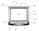
図1及び図2において、本実施形態に係る電気光学装置では、TFTアレイ基板10と対向基板20とが対向配置されている。TFTアレイ基板10は、例えば石英基板、ガラス基板等の透明基板や、シリコン基板等である。対向基板20は、例えば石英基板、ガラス基板等の透明基板である。TFTアレイ基板10と対向基板20との間には、液晶層50が封入されている。液晶層50は、例えば一種又は数種類のネマティック液晶を混合した液晶からなり、一対の配向膜間で所定の配向状態をとる。
1 and 2, in the electro-optical device according to the present embodiment, a
TFTアレイ基板10と対向基板20とは、複数の画素電極が設けられた画像表示領域10aの周囲に位置するシール領域に設けられたシール材52により、相互に接着されている。
The
シール材52は、両基板を貼り合わせるための、例えば紫外線硬化樹脂、熱硬化樹脂等からなり、製造プロセスにおいてTFTアレイ基板10上に塗布された後、紫外線照射、加熱等により硬化させられたものである。シール材52中には、TFTアレイ基板10と対向基板20との間隔(即ち、基板間ギャップ)を所定値とするためのグラスファイバー或いはガラスビーズ等のギャップ材が散布されている。尚、ギャップ材を、シール材52に混入されるものに加えて若しくは代えて、画像表示領域10a又は画像表示領域10aの周辺に位置する周辺領域に、配置するようにしてもよい。
The sealing
シール材52が配置されたシール領域の内側に並行して、画像表示領域10aの額縁領域を規定する遮光性の額縁遮光膜53が、対向基板20側に設けられている。尚、このような額縁遮光膜53の一部又は全部は、TFTアレイ基板10側に内蔵遮光膜として設けられてもよい。
A light-shielding frame light-shielding
周辺領域のうち、シール材52が配置されたシール領域の外側に位置する領域には、データ線駆動回路101及び外部回路接続端子102がTFTアレイ基板10の一辺に沿って設けられている。走査線駆動回路104は、この一辺に隣接する2辺に沿い、且つ、額縁遮光膜53に覆われるようにして設けられている。更に、このように画像表示領域10aの両側に設けられた二つの走査線駆動回路104間をつなぐため、TFTアレイ基板10の残る一辺に沿い、且つ、額縁遮光膜53に覆われるようにして複数の配線105が設けられている。
A data
TFTアレイ基板10上における対向基板20の4つのコーナー部に対向する領域には、両基板間を上下導通材で接続するための上下導通端子106が配置されている。これらにより、TFTアレイ基板10と対向基板20との間で電気的な導通をとることができる。
In a region facing the four corners of the
図2において、TFTアレイ基板10上には、駆動素子である画素スイッチング用のTFTや走査線、データ線等の配線が作り込まれた積層構造が形成される。この積層構造の詳細な構成については図2では図示を省略してあるが、この積層構造の上に、ITO等の透明材料からなる画素電極9aが、画素毎に所定のパターンで島状に形成されている。
In FIG. 2, on the
画素電極9aは、対向電極21に対向するように、TFTアレイ基板10上の画像表示領域10aに形成されている。TFTアレイ基板10における液晶層50の面する側の表面、即ち画素電極9a上には、配向膜16が画素電極9aを覆うように形成されている。
The
対向基板20におけるTFTアレイ基板10との対向面上には、遮光膜23が形成されている。遮光膜23は、例えば対向基板20における対向面上に平面的に見て、格子状に形成されている。対向基板20において、遮光膜23によって非開口領域が規定され、遮光膜23によって区切られた領域が、例えばプロジェクター用のランプや直視用のバックライトから出射された光を透過させる開口領域となる。尚、遮光膜23をストライプ状に形成し、該遮光膜23と、TFTアレイ基板10側に設けられたデータ線等の各種構成要素とによって、非開口領域を規定するようにしてもよい。
A
遮光膜23上には、ITO等の透明材料からなる対向電極21が複数の画素電極9aと対向するように形成されている。また遮光膜23上には、画像表示領域10aにおいてカラー表示を行うために、開口領域及び非開口領域の一部を含む領域に、図2には図示しないカラーフィルターが形成されるようにしてもよい。対向基板20の対向面上における、対向電極21上には、配向膜22が形成されている。
On the
尚、図1及び図2に示したTFTアレイ基板10上には、上述したデータ線駆動回路101、走査線駆動回路104等の駆動回路に加えて、画像信号線上の画像信号をサンプリングしてデータ線に供給するサンプリング回路、複数のデータ線に所定電圧レベルのプリチャージ信号を画像信号に先行して各々供給するプリチャージ回路、製造途中や出荷時の当該電気光学装置の品質、欠陥等を検査するための検査回路等を形成してもよい。
In addition to the above-described drive circuits such as the data
次に、本実施形態に係る電気光学装置の画素部の電気的な構成について、図3を参照して説明する。ここに図3は、本実施形態に係る電気光学装置の画像表示領域を構成するマトリクス状に形成された複数の画素における各種素子、配線等の等価回路図である。 Next, an electrical configuration of the pixel portion of the electro-optical device according to the present embodiment will be described with reference to FIG. FIG. 3 is an equivalent circuit diagram of various elements, wirings, and the like in a plurality of pixels formed in a matrix forming the image display area of the electro-optical device according to this embodiment.
図3において、画像表示領域10aを構成するマトリクス状に形成された複数の画素の各々には、画素電極9a及びTFT30が形成されている。TFT30は、画素電極9aに電気的に接続されており、本実施形態に係る電気光学装置の動作時に画素電極9aをスイッチング制御する。画像信号が供給されるデータ線6aは、TFT30のソースに電気的に接続されている。データ線6aに書き込む画像信号S1、S2、・・・、Snは、この順に線順次に供給しても構わないし、相隣接する複数のデータ線6a同士に対して、グループ毎に供給するようにしてもよい。
In FIG. 3, a
TFT30のゲートには、走査線3aが電気的に接続されており、本実施形態に係る電気光学装置は、所定のタイミングで、走査線3aにパルス的に走査信号G1、G2、・・・、Gmを、この順に線順次で印加するように構成されている。画素電極9aは、TFT30のドレインに電気的に接続されており、スイッチング素子であるTFT30を一定期間だけそのスイッチを閉じることにより、データ線6aから供給される画像信号S1、S2、・・・、Snが所定のタイミングで書き込まれる。画素電極9aを介して電気光学物質の一例としての液晶に書き込まれた所定レベルの画像信号S1、S2、・・・、Snは、対向基板に形成された対向電極との間で一定期間保持される。
The
液晶層50(図2参照)を構成する液晶は、印加される電圧レベルにより分子集合の配向や秩序が変化することにより、光を変調し、階調表示を可能とする。例えば、ノーマリーホワイトモードであれば、各画素の単位で印加された電圧に応じて入射光に対する透過率が減少し、ノーマリーブラックモードであれば、各画素の単位で印加された電圧に応じて入射光に対する透過率が増加され、全体として電気光学装置からは画像信号に応じたコントラストをもつ光が出射される。 The liquid crystal constituting the liquid crystal layer 50 (see FIG. 2) modulates light and enables gradation display by changing the orientation and order of the molecular assembly depending on the applied voltage level. For example, in the normally white mode, the transmittance for incident light is reduced according to the voltage applied in units of each pixel. In the normally black mode, the transmittance is applied in units of each pixel. As a result, the transmittance for incident light is increased, and light having a contrast corresponding to an image signal is emitted from the electro-optical device as a whole.
ここで保持された画像信号がリークすることを防ぐために、画素電極9aと対向電極21(図2参照)との間に形成される液晶容量と並列に蓄積容量70が付加されている。蓄積容量70は、画像信号の供給に応じて各画素電極9aの電位を一時的に保持する保持容量として機能する容量素子である。蓄積容量70の一方の電極は、画素電極9aと並列してTFT30のドレインに電気的に接続され、他方の電極は、定電位となるように、電位固定の容量線300に電気的に接続されている。蓄積容量70によれば、画素電極9aにおける電位保持特性が向上し、コントラスト向上やフリッカーの低減といった表示特性の向上が可能となる。
In order to prevent the image signal held here from leaking, a
次に、本実施形態に係る電気光学装置に特有の層構造について、図4から図7を参照して説明する。ここに図4は、実施形態に係る電気光学装置における交差領域の具体的な構成を示す平面図であり、図5は、図4のA−A´線断面図である。また図6は、実施形態に係る導電層の製造工程を示す工程断面図であり、図7は、比較例に係る導電層の構成を示す断面図である。尚、図4以降の図では、説明の便宜上、装置を構成する各層のうち本実施形態に関わりの深い層のみを図示し、その他の層については適宜図示を省略している。 Next, a layer structure unique to the electro-optical device according to the present embodiment will be described with reference to FIGS. FIG. 4 is a plan view showing a specific configuration of the intersecting region in the electro-optical device according to the embodiment, and FIG. 5 is a cross-sectional view taken along the line AA ′ of FIG. FIG. 6 is a process cross-sectional view illustrating the manufacturing process of the conductive layer according to the embodiment, and FIG. 7 is a cross-sectional view illustrating the configuration of the conductive layer according to the comparative example. In FIG. 4 and subsequent figures, for convenience of explanation, only the layers deeply related to the present embodiment are shown among the layers constituting the apparatus, and the other layers are omitted as appropriate.
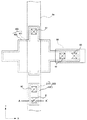
図4において、本実施形態に係る電気光学装置は、データ線6a及びデータ線6aと同層に形成された第3中継層90と、第1中継層200及び第1中継層200と同層に形成された第2中継層400とを備えて構成されている。データ線6a及び第3中継層90、並びに第1中継層200及び第2中継層400は、夫々遮光性を有する材料を含んでおり、画素領域における非開口領域を規定している。
4, the electro-optical device according to the present embodiment includes the
データ線6aは、コンタクトホール81を介して、下層側の第1中継層200と電気的に接続されている。第1中継層200は、コンタクトホール82を介して、下層側の導電層(例えば、TFT30を構成する半導体層のソース領域)に電気的に接続されている。
The
第2中継層は、コンタクトホール83を介して、下層側の導電層(例えば、TFT30を構成する半導体層のドレイン領域)に電気的に接続されている。また第2中継層は、コンタクトホール84を介して、上層側の第3中継層90と電気的に接続されている。第3中継層90は、コンタクトホール85を介して、上層側の導電層(例えば、画素電極)と電気的に接続されている。
The second relay layer is electrically connected to the lower conductive layer (for example, the drain region of the semiconductor layer constituting the TFT 30) via the
ここで特に、第1中継層200は、導電層210と、導電層210を上層側から覆うように形成された反射防止層220とを備えている。また、第1中継層200と同層に形成された第2中継層400も同様に、導電層410と、導電層410を上層側から覆うように形成された反射防止層420とを備えている。
Here, in particular, the
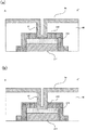
図5において、導電層210は、第1の層211及び第1の層211の上層に積層された第2の層212から構成されている。第1の層211は、本発明の「導電層」の一例であり、例えばアルミニウム等の比較的導電性の高い材料を含んで構成されている。第2の層212は、本発明の「保護層」の一例であり、例えば導電性を有すると共に比較的酸化し難いTiN(チタンナイトライド)等を含んで構成されている。反射防止層220は、本発明の「反射防止膜」の一例であり、例えばTiNやW(タングステン)等の導電層より光反射率の低い材料を含んでいる。反射防止層220は特に、第1の層211及び第2の層212の端面(即ち、縦方向に切り立った部分)を覆うように形成されている。
In FIG. 5, the
図5(a)において、データ線6aは、反射防止層220より層間絶縁膜40を介して上層に形成されており、層間絶縁膜40を貫通するように形成されたコンタクトホール81を介して、反射防止膜220と電気的に接続されている。或いは図5(b)に示すように、データ線6aは、層間絶縁膜40及び反射防止層220を貫通するように形成されたコンタクトホール81を介して、保護層212と電気的に接続されてもよい。
In FIG. 5A, the
ここで特に、本願発明者の研究によれば、第1の層211及び第2の層212の端面は、動作時に入射される光源光を反射してしまうことによって光漏れを生じ易い箇所である。よって、仮に何らの対策も講じないとすれば、光漏れに起因して表示画像のコントラストが低下し、画質の低下を引き起こしてしまうおそれがある。
In particular, according to the study of the present inventor, the end surfaces of the
しかるに本実施形態に係る電気光学装置では特に、第1の層211及び第2の層212の端面を覆うように反射防止層220が形成されている。よって、第1の層211及び第2の層212の端面における光の反射が抑制され、光漏れの発生を低減させることができる。尚、本実施形態に係る反射防止層220は、第1の層211及び第2の層212の端面全てを覆うように形成されているが、光漏れを生じ易い部分でのみ端面を覆うように形成されてもよい。
However, in the electro-optical device according to this embodiment, the
図6において、第1の層211及び第2の層212は、夫々を構成する2つの膜が形成された後に一緒にパターニングされることで、互いに同じ領域に形成される。具体的には、第1の層211の上層に第2の層212を形成した後に、第1の層211及び第2の層212がまとめてエッチングされる。その後、第1の層211及び第2の層212の上層に反射防止層220が形成されることで、図5に示すような構成とされる。
In FIG. 6, the
図7に示すように、仮に第1の層211の上層に第2の層212が形成されていないとすると、アルミニウム等で構成された第1の層211と、チタンナイトライド等で構成された反射防止膜220との界面に酸化膜系の絶縁膜が形成され、第1中継層200全体としての抵抗値が高くなってしまうおそれがある。
As shown in FIG. 7, if the
これに対し、本実施形態に係る電気光学装置は、図6で示すように第1の層211の上層に第2の層212が形成されるため、上述した酸化膜の形成を防止することができる。よって、酸化膜が形成されることに起因する高抵抗化を防止することができる。従って、表示画像の品質を更に向上させることが可能である。
On the other hand, since the
また第2の層212は、上層側のコンタクトホール81を形成する際の保護層としても機能する。具体的には、図5に示すように、コンタクトホール81は、反射防止膜220又は第2の層212が露出するように形成されればよいため、形成する際のマージンが確保できる。即ち、コンタクトホール81を形成する際のエッチングに高い精度が求められなくなる。
The
以上説明したように、本実施形態に係る電気光学装置によれば、第1の層211を第2の層212で覆うことによって、装置の製造を容易なものとすることが可能であると共に、高抵抗化を防止することができる。更に、第1の層211及び第2の層212の端面を反射防止膜で覆うことによって、表示領域における光漏れの発生を抑制することができる。その結果、高いコントラスト比を有する高品位な画像表示を実現可能である。
As described above, according to the electro-optical device according to this embodiment, the
尚、本実施形態では、第1中継層200(図4参照)を例にとり説明したが、同様に構成された第2中継層400においても、上述した効果は得られる。また、第1中継層200及び第2中継層400以外の導電層(例えば、走査線3aやデータ線6a)等を、同様の層構造とすることも可能である。
In the present embodiment, the first relay layer 200 (see FIG. 4) has been described as an example. However, the above-described effects can be obtained also in the
<電子機器>
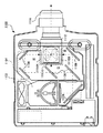
次に、上述した電気光学装置である液晶装置を各種の電子機器に適用する場合について説明する。ここに図8は、プロジェクターの構成例を示す平面図である。以下では、この液晶装置をライトバルブとして用いたプロジェクターについて説明する。
<Electronic equipment>
Next, the case where the liquid crystal device which is the above-described electro-optical device is applied to various electronic devices will be described. FIG. 8 is a plan view showing a configuration example of the projector. Hereinafter, a projector using the liquid crystal device as a light valve will be described.
図8に示されるように、プロジェクター1100内部には、ハロゲンランプ等の白色光源からなるランプユニット1102が設けられている。このランプユニット1102から射出された投射光は、ライトガイド1104内に配置された4枚のミラー1106及び2枚のダイクロイックミラー1108によってRGBの3原色に分離され、各原色に対応するライトバルブとしての液晶パネル1110R、1110B及び1110Gに入射される。
As shown in FIG. 8, a
液晶パネル1110R、1110B及び1110Gの構成は、上述した液晶装置と同等であり、画像信号処理回路から供給されるR、G、Bの原色信号でそれぞれ駆動されるものである。そして、これらの液晶パネルによって変調された光は、ダイクロイックプリズム1112に3方向から入射される。このダイクロイックプリズム1112においては、R及びBの光が90度に屈折する一方、Gの光が直進する。従って、各色の画像が合成される結果、投射レンズ1114を介して、スクリーン等にカラー画像が投写されることとなる。
The configurations of the
ここで、各液晶パネル1110R、1110B及び1110Gによる表示像について着目すると、液晶パネル1110Gによる表示像は、液晶パネル1110R、1110Bによる表示像に対して左右反転することが必要となる。
Here, paying attention to the display images by the
尚、液晶パネル1110R、1110B及び1110Gには、ダイクロイックミラー1108によって、R、G、Bの各原色に対応する光が入射するので、カラーフィルターを設ける必要はない。
Since light corresponding to the primary colors R, G, and B is incident on the
尚、図8を参照して説明した電子機器の他にも、モバイル型のパーソナルコンピュータや、携帯電話、液晶テレビや、ビューファインダー型、モニタ直視型のビデオテープレコーダー、カーナビゲーション装置、ページャー、電子手帳、電卓、ワードプロセッサー、ワークステーション、テレビ電話、POS端末、タッチパネルを備えた装置等が挙げられる。そして、これらの各種電子機器に適用可能なのは言うまでもない。 In addition to the electronic device described with reference to FIG. 8, a mobile personal computer, a mobile phone, an LCD TV, a viewfinder type, a monitor direct view type video tape recorder, a car navigation device, a pager, an electronic device Examples include notebooks, calculators, word processors, workstations, videophones, POS terminals, and devices with touch panels. Needless to say, the present invention can be applied to these various electronic devices.
また、本発明は上述の各実施形態で説明した液晶装置以外にも反射型液晶装置(LCOS)、プラズマディスプレイ(PDP)、電界放出型ディスプレイ(FED、SED)、有機ELディスプレイ、デジタルマイクロミラーデバイス(DMD)、電気泳動装置等にも適用可能である。 In addition to the liquid crystal devices described in the above embodiments, the present invention includes a reflective liquid crystal device (LCOS), a plasma display (PDP), a field emission display (FED, SED), an organic EL display, and a digital micromirror device. (DMD), electrophoresis apparatus and the like are also applicable.
本発明は、上述した実施形態に限られるものではなく、特許請求の範囲及び明細書全体から読み取れる発明の要旨或いは思想に反しない範囲で適宜変更可能であり、そのような変更を伴う電気光学装置、及び該電気光学装置を備えた電子機器もまた本発明の技術的範囲に含まれるものである。 The present invention is not limited to the above-described embodiments, and can be appropriately changed without departing from the spirit or idea of the invention that can be read from the claims and the entire specification, and an electro-optical device with such a change. In addition, an electronic apparatus including the electro-optical device is also included in the technical scope of the present invention.
3a…走査線、6a…データ線、9a…画素電極、10…TFTアレイ基板、10a…画像表示領域、20…対向基板、30…TFT、40…層間絶縁膜、50…液晶層、70…蓄積容量、81,82,83,84,85…コンタクトホール、90…第3中継層、200…第1中継層、210…導電層、211…第1の層、212…第2の層、220…反射防止層、400…第2中継層、410…導電層、420…反射防止層 3a ... Scanning line, 6a ... Data line, 9a ... Pixel electrode, 10 ... TFT array substrate, 10a ... Image display area, 20 ... Counter substrate, 30 ... TFT, 40 ... Interlayer insulating film, 50 ... Liquid crystal layer, 70 ... Storage Capacity, 81, 82, 83, 84, 85 ... contact hole, 90 ... third relay layer, 200 ... first relay layer, 210 ... conductive layer, 211 ... first layer, 212 ... second layer, 220 ... Antireflection layer, 400 ... second relay layer, 410 ... conductive layer, 420 ... antireflection layer
Claims (6)
前記画素電極が配列された画素領域に配置された導電層と、
前記導電層を挟んで基板と対向するように配置される保護層と、
前記導電層より光反射率の低い材料を含んでおり、前記導電層及び前記保護層を挟んで前記基板に対向するように配置される反射防止膜と、
前記反射防止膜を挟んで前記基板に対向するように配置される絶縁膜と、
前記絶縁膜から前記基板に向かう方向から見て、前記絶縁膜の前記導電層及び前記保護膜と重なる位置に形成されたコンタクトホールと、
を含み、
前記反射防止膜は、前記導電層の端面及び前記保護層の端面を少なくとも部分的に覆い、
前記方向から見て、前記コンタクトホールは、データ線と重なることを特徴とする電気光学装置。 A pixel electrode;
A conductive layer disposed in a pixel region in which the pixel electrodes are arranged;
A protective layer disposed to face the substrate across the conductive layer;
An antireflection film including a material having a light reflectance lower than that of the conductive layer, and disposed so as to face the substrate with the conductive layer and the protective layer interposed therebetween;
An insulating film disposed to face the substrate across the antireflection film;
A contact hole formed at a position overlapping the conductive layer and the protective film of the insulating film when viewed from the direction from the insulating film toward the substrate;
Including
The antireflection film at least partially covers an end face of the conductive layer and an end face of the protective layer ;
The electro-optical device , wherein the contact hole overlaps with the data line when viewed from the direction .
前記電極は前記反射防止膜又は前記保護層と電気的に接続されることを特徴とする請求項1に記載の電気光学装置。 An electrode disposed in the contact hole;
The electro-optical device according to claim 1, wherein the electrode is electrically connected to the antireflection film or the protective layer.
前記反射防止膜は、前記第1部分及び前記第2部分が互いに交差する交差領域において前記導電層及び前記保護層の端面を覆うように形成されていることを特徴とする請求項1から4のいずれか一項に記載の電気光学装置。 The conductive layer has a first portion extending in a first direction and a second portion extending in a second direction intersecting the first direction;
The antireflection film is formed so as to cover end surfaces of the conductive layer and the protective layer in an intersecting region where the first portion and the second portion intersect each other. The electro-optical device according to any one of the above.
Priority Applications (1)
| Application Number | Priority Date | Filing Date | Title |
|---|---|---|---|
| JP2010032143A JP5482279B2 (en) | 2010-02-17 | 2010-02-17 | Electro-optical device and electronic apparatus |
Applications Claiming Priority (1)
| Application Number | Priority Date | Filing Date | Title |
|---|---|---|---|
| JP2010032143A JP5482279B2 (en) | 2010-02-17 | 2010-02-17 | Electro-optical device and electronic apparatus |
Publications (3)
| Publication Number | Publication Date |
|---|---|
| JP2011170007A JP2011170007A (en) | 2011-09-01 |
| JP2011170007A5 JP2011170007A5 (en) | 2013-03-21 |
| JP5482279B2 true JP5482279B2 (en) | 2014-05-07 |
Family
ID=44684223
Family Applications (1)
| Application Number | Title | Priority Date | Filing Date |
|---|---|---|---|
| JP2010032143A Expired - Fee Related JP5482279B2 (en) | 2010-02-17 | 2010-02-17 | Electro-optical device and electronic apparatus |
Country Status (1)
| Country | Link |
|---|---|
| JP (1) | JP5482279B2 (en) |
Family Cites Families (5)
| Publication number | Priority date | Publication date | Assignee | Title |
|---|---|---|---|---|
| JP3912064B2 (en) * | 2001-09-21 | 2007-05-09 | セイコーエプソン株式会社 | ELECTRO-OPTICAL DEVICE, MANUFACTURING METHOD THEREOF, AND ELECTRONIC DEVICE |
| JP4506133B2 (en) * | 2002-10-31 | 2010-07-21 | セイコーエプソン株式会社 | Electro-optical device and electronic apparatus |
| JP2005148387A (en) * | 2003-11-14 | 2005-06-09 | Seiko Epson Corp | Method for manufacturing electrooptical device, electrooptical device, and electronic equipment provided with the same |
| JP2005333042A (en) * | 2004-05-21 | 2005-12-02 | Sony Corp | Electrooptical display device and method for manufacturing same |
| JP4123245B2 (en) * | 2004-08-20 | 2008-07-23 | セイコーエプソン株式会社 | Electro-optical device and electronic apparatus |
-
2010
- 2010-02-17 JP JP2010032143A patent/JP5482279B2/en not_active Expired - Fee Related
Also Published As
| Publication number | Publication date |
|---|---|
| JP2011170007A (en) | 2011-09-01 |
Similar Documents
| Publication | Publication Date | Title |
|---|---|---|
| JP5589359B2 (en) | Electro-optical device and electronic apparatus | |
| JP5217752B2 (en) | Electro-optical device and electronic apparatus | |
| JP5211985B2 (en) | Electro-optical device and electronic apparatus | |
| JP5287100B2 (en) | Electro-optical device and electronic apparatus | |
| JP5488136B2 (en) | Electro-optical device, electronic device, and transistor | |
| JP5187067B2 (en) | Electro-optical device and electronic apparatus | |
| JP5499736B2 (en) | Electro-optical device and electronic apparatus | |
| JP5278129B2 (en) | Electro-optical device and electronic apparatus | |
| JP5445115B2 (en) | Electro-optical device and electronic apparatus | |
| JP2010096966A (en) | Electro-optical apparatus, method for manufacturing same, and electronic device | |
| JP6048553B2 (en) | Electro-optical device and electronic apparatus | |
| JP5200720B2 (en) | Electro-optical device, electronic apparatus, and method of manufacturing electro-optical device | |
| JP5233618B2 (en) | Electro-optical device and electronic apparatus | |
| JP2007212819A (en) | Electro-optical device, substrate for electro-optical device, manufacturing method of electro-optical device, and electronic equipment | |
| JP2009069247A (en) | Electro-optical apparatus, manufacturing method thereof, electronic equipment, and wiring structure | |
| JP5182116B2 (en) | Electro-optical device and electronic apparatus | |
| JP2010191408A (en) | Electro-optical device and electronic apparatus | |
| JP5470894B2 (en) | Electro-optical device and electronic apparatus | |
| JP5482279B2 (en) | Electro-optical device and electronic apparatus | |
| JP2011180524A (en) | Electro-optical device and electronic equipment | |
| JP2011075773A (en) | Electro-optical apparatus and electric apparatus | |
| JP2010186118A (en) | Electro-optical device and electronic apparatus | |
| JP5804113B2 (en) | Electro-optical device and electronic apparatus | |
| JP2010160308A (en) | Electrooptical apparatus and electronic device | |
| JP2011186283A (en) | Electrooptical device and electronic apparatus |
Legal Events
| Date | Code | Title | Description |
|---|---|---|---|
| A521 | Written amendment |
Free format text: JAPANESE INTERMEDIATE CODE: A523 Effective date: 20130201 |
|
| A621 | Written request for application examination |
Free format text: JAPANESE INTERMEDIATE CODE: A621 Effective date: 20130201 |
|
| A977 | Report on retrieval |
Free format text: JAPANESE INTERMEDIATE CODE: A971007 Effective date: 20130829 |
|
| A131 | Notification of reasons for refusal |
Free format text: JAPANESE INTERMEDIATE CODE: A131 Effective date: 20130903 |
|
| A521 | Written amendment |
Free format text: JAPANESE INTERMEDIATE CODE: A523 Effective date: 20131028 |
|
| TRDD | Decision of grant or rejection written | ||
| A01 | Written decision to grant a patent or to grant a registration (utility model) |
Free format text: JAPANESE INTERMEDIATE CODE: A01 Effective date: 20140121 |
|
| A61 | First payment of annual fees (during grant procedure) |
Free format text: JAPANESE INTERMEDIATE CODE: A61 Effective date: 20140203 |
|
| R150 | Certificate of patent or registration of utility model |
Ref document number: 5482279 Country of ref document: JP Free format text: JAPANESE INTERMEDIATE CODE: R150 |
|
| S531 | Written request for registration of change of domicile |
Free format text: JAPANESE INTERMEDIATE CODE: R313531 |
|
| R350 | Written notification of registration of transfer |
Free format text: JAPANESE INTERMEDIATE CODE: R350 |
|
| LAPS | Cancellation because of no payment of annual fees |