JP5477179B2 - 電気泳動表示装置および電子機器 - Google Patents
電気泳動表示装置および電子機器 Download PDFInfo
- Publication number
- JP5477179B2 JP5477179B2 JP2010131896A JP2010131896A JP5477179B2 JP 5477179 B2 JP5477179 B2 JP 5477179B2 JP 2010131896 A JP2010131896 A JP 2010131896A JP 2010131896 A JP2010131896 A JP 2010131896A JP 5477179 B2 JP5477179 B2 JP 5477179B2
- Authority
- JP
- Japan
- Prior art keywords
- electrode
- branch
- pixel
- substrate
- width
- Prior art date
- Legal status (The legal status is an assumption and is not a legal conclusion. Google has not performed a legal analysis and makes no representation as to the accuracy of the status listed.)
- Expired - Fee Related
Links
Images


Classifications
-
- G—PHYSICS
- G09—EDUCATION; CRYPTOGRAPHY; DISPLAY; ADVERTISING; SEALS
- G09G—ARRANGEMENTS OR CIRCUITS FOR CONTROL OF INDICATING DEVICES USING STATIC MEANS TO PRESENT VARIABLE INFORMATION
- G09G3/00—Control arrangements or circuits, of interest only in connection with visual indicators other than cathode-ray tubes
- G09G3/20—Control arrangements or circuits, of interest only in connection with visual indicators other than cathode-ray tubes for presentation of an assembly of a number of characters, e.g. a page, by composing the assembly by combination of individual elements arranged in a matrix no fixed position being assigned to or needed to be assigned to the individual characters or partial characters
- G09G3/34—Control arrangements or circuits, of interest only in connection with visual indicators other than cathode-ray tubes for presentation of an assembly of a number of characters, e.g. a page, by composing the assembly by combination of individual elements arranged in a matrix no fixed position being assigned to or needed to be assigned to the individual characters or partial characters by control of light from an independent source
- G09G3/3433—Control arrangements or circuits, of interest only in connection with visual indicators other than cathode-ray tubes for presentation of an assembly of a number of characters, e.g. a page, by composing the assembly by combination of individual elements arranged in a matrix no fixed position being assigned to or needed to be assigned to the individual characters or partial characters by control of light from an independent source using light modulating elements actuated by an electric field and being other than liquid crystal devices and electrochromic devices
- G09G3/344—Control arrangements or circuits, of interest only in connection with visual indicators other than cathode-ray tubes for presentation of an assembly of a number of characters, e.g. a page, by composing the assembly by combination of individual elements arranged in a matrix no fixed position being assigned to or needed to be assigned to the individual characters or partial characters by control of light from an independent source using light modulating elements actuated by an electric field and being other than liquid crystal devices and electrochromic devices based on particles moving in a fluid or in a gas, e.g. electrophoretic devices
- G09G3/3446—Control arrangements or circuits, of interest only in connection with visual indicators other than cathode-ray tubes for presentation of an assembly of a number of characters, e.g. a page, by composing the assembly by combination of individual elements arranged in a matrix no fixed position being assigned to or needed to be assigned to the individual characters or partial characters by control of light from an independent source using light modulating elements actuated by an electric field and being other than liquid crystal devices and electrochromic devices based on particles moving in a fluid or in a gas, e.g. electrophoretic devices with more than two electrodes controlling the modulating element
-
- G—PHYSICS
- G09—EDUCATION; CRYPTOGRAPHY; DISPLAY; ADVERTISING; SEALS
- G09G—ARRANGEMENTS OR CIRCUITS FOR CONTROL OF INDICATING DEVICES USING STATIC MEANS TO PRESENT VARIABLE INFORMATION
- G09G2300/00—Aspects of the constitution of display devices
- G09G2300/04—Structural and physical details of display devices
- G09G2300/0421—Structural details of the set of electrodes
- G09G2300/0426—Layout of electrodes and connections
-
- G—PHYSICS
- G09—EDUCATION; CRYPTOGRAPHY; DISPLAY; ADVERTISING; SEALS
- G09G—ARRANGEMENTS OR CIRCUITS FOR CONTROL OF INDICATING DEVICES USING STATIC MEANS TO PRESENT VARIABLE INFORMATION
- G09G2300/00—Aspects of the constitution of display devices
- G09G2300/08—Active matrix structure, i.e. with use of active elements, inclusive of non-linear two terminal elements, in the pixels together with light emitting or modulating elements
- G09G2300/0809—Several active elements per pixel in active matrix panels
- G09G2300/0814—Several active elements per pixel in active matrix panels used for selection purposes, e.g. logical AND for partial update
Description
意図しない粒子が共通電極側に残ってしまうと表示ムラが生じてしまう。
本発明によれば、全ての帯電粒子に対して電界が作用してそれらの移動を制御することができ、意図しない粒子が第2電極側に残ることが防止されて、表示ムラが生じるのを抑制することが可能になる。
本発明によれば、各枝部どうしの間でリーク電流が発生しない長さであれば、第1の枝部の幅を第2の枝部の幅の1/3以上の長さに設定しても良く、これによって、全ての帯電粒子に対して電界が作用してそれらの移動を制御することができ、意図しない粒子が共通電極側に残ることが防止されて、表示ムラが生じるのを抑制することが可能になる。
本発明によれば、全ての帯電粒子に対して電界が作用してそれらの移動を制御することができ、意図しない粒子が第2電極側に残ることが防止されて、表示ムラが生じるのを抑制することが可能になる。
本発明によれば、低消費電力で駆動でき、かつ、表示ムラのない高品位な表示部を備えた電子機器が得られる。
図1に示すように、電気泳動表示装置100の表示部5には、複数の画素40がマトリクス状に配列されている。表示部5の周辺には、走査線駆動回路61およびデータ線駆動回路62が配置されている。走査線駆動回路61およびデータ線駆動回路62は、それぞれコントローラー(不図示)と接続されている。コントローラーは、上位装置から供給される画像データや同期信号に基づき、走査線駆動回路61およびデータ線駆動回路62を総合的に制御する。
図2に示すように、本実施形態の電気泳動表示装置100では、1つの画素40内に2つの選択トランジスタTR1,TR2および2つの画素電極35A,35Bが設けられている。各画素40における画素回路は、電気光学材料としての電気泳動層32と、この電気泳動層32に電圧を供給するためのスイッチング動作を行う選択トランジスタTR1,TR2と、これら選択トランジスタTR1,TR2にそれぞれ接続される画素電極35A,35Bと、共通電極37とを含んでそれぞれ構成されている。2つの選択トランジスタTR1,TR2で画素電極35A,35Bへの印加電圧を独立に制御することでクロストークのない画像表示を行うことができる。
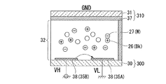
図3に示すように、電気泳動表示装置100は、素子基板300(第1基板)と対向基板310(第2基板)との間に、3粒子系の電気泳動層32が設けられた構成を備えている。電気泳動層32は、透明な分散媒21(T)中にプラスに帯電した黒色の正帯電粒子26(Bk)、マイナスに帯電した白色の負帯電粒子27(W)と、赤色の無帯電粒子28(R)とが保持されてなる。帯電した粒子(正帯電粒子26(Bk)、負帯電粒子27(W))は、電気泳動層32中において電気泳動粒子として振る舞う。観測者は第2基板31側から表示を観察するものとする。
このような対向基板310は、各画素領域を区画する隔壁13を介して素子基板300上に対向配置されている。
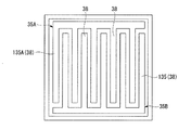
図4に示すように、画素電極35Aおよび画素電極35Bは、走査線66A,66Bに沿って延在する幹部36と、当該幹部36によって連結された複数の枝部38とを有してなり、互いの枝部38が噛み合うようにして配置されている。つまり、画素電極35Aの枝部38の両側に、画素電極35Bの枝部38が存在する状態となっている。画素電極35A,35Bの形状を櫛歯形状にすることで、画素電極35A,35B間で粒子が移動しやすいようになっている。
素子基板300の具体的な構成については、図5に示すように、厚さ0.6mmのガラス基板からなる第1基板30の表面上に厚さ300nmのアルミニウム(Al)からなるゲート電極41eを覆うようにして第1基板30の表面全体に酸化シリコン膜からなるゲート絶縁膜41bが形成され、ゲート電極41eの直上に厚さ50nmのa−IGZO(In、Ga、Znの酸化物)からなる半導体層41aが形成されている。
また、各画素電極35A,35Bに印加される正の電圧のうち絶対値が最大となる電圧を電圧VH(以下、正の最大値とも称する)、負の電圧のうち絶対値が最大となる電圧を電圧VL(以下、負の最大値とも称する)とする。
なお、「電極に電圧を印加する」とは、「電極に対して、グランド電位との間で当該電圧を生じさせるような電位を供給する」ことと同義である。
黒表示にする場合は、画素電極35Aおよび画素電極35Bにそれぞれプラス電圧VHを印加し、共通電極37にマイナス電圧VLを印加する。すると、この電圧VHに対応する電位と共通電極37のグランド電位との電位差(電圧)に起因する電界によって、プラスに帯電した正帯電粒子26(Bk)が全て共通電極37側へと移動して、マイナスに帯電した複数の負帯電粒子27(W)が画素電極35Aおよび画素電極35B上に吸着した状態となる。外部から入射した光は共通電極37上に分布する正帯電粒子26(Bk)にて散乱され、黒色となって共通電極37側から出光する。
黒表示から白表示に切り替える場合、図6(a)に示した状態から電圧を印加することになる。白表示に切り替えるために、画素電極35Aおよび画素電極35Bにそれぞれマイナス電圧VLを印加し、共通電極37にプラス電圧VHを印加する。すると、画素電極35B上の全ての負帯電粒子27(W)が共通電極37側へと移動して、今度は、正帯電粒子26(Bk)が画素電極35Aおよび画素電極35B上に吸着した状態となる。外部から入射した光は共通電極37上に分布する負帯電粒子27(W)にて散乱され、白色となって共通電極37側から出光する。
白表示から赤表示に切り替える場合、図6(b)に示した状態から電圧を印加することになる。赤表示に切り替えるために、画素電極35Aにプラス電圧VHを印加し、画素電極35Bにマイナス電圧VLを印加し、共通電極37には画素電極35Aに印加したプラス電圧VHと画素電極35Bに印加したマイナス電圧VLとの中間の電圧VM(VL<VM<VH)を印加する。すると、画素電極35A上に負帯電粒子27(W)が吸着し、画素電極35B上に正帯電粒子26(Bk)が吸着する。外部から入射した光は分散媒21(T)中を浮遊する赤色の無帯電粒子28(R)にて散乱され、赤色となって共通電極37側から出光する。
ここで、粒子27(W)による白表示には、入射光が粒子により複数回散乱されることが必要なため、電気泳動層32内の3次元的な深さ方向の分布も必要になる。上記した視認される面積とは、粒子の2次元、3次元的分布を含めて実際に視認される実効的な面積をさす。
以上説明したように、正帯電粒子26(Bk)、負帯電粒子27(W)の移動量および分布範囲を制御することによって、各画素における明度の制御が可能である。
例えば、画素電極35Aの枝部38上における共通電極37側に分布している粒子に対しては、当該枝部38の両側に配置されている画素電極35Bの枝部38,38のうちのいずれかの電界が作用することとなる。
したがって、本実施形態の構成によれば、1画素内における画素電極35A,35B間の境界長さを低減させることで画素電極35A,35B間に発生するリーク電流を低減しつつ、画素回路の端部でも良好な表示を得ることができる。
また、カプセル型の電気泳動材料を用いても良い。
次に、上記各実施形態の電気泳動表示装置を電子機器に適用した場合について説明する。
図8は、本発明の電気泳動表示装置を適用した電子機器の具体例を説明する斜視図である。
図8(a)は、電子機器の一例である電子ブックを示す斜視図である。この電子ブック1000は、ブック形状のフレーム1001と、このフレーム1001に対して回動自在に設けられた(開閉可能な)カバー1002と、操作部1003と、本発明の電気泳動表示装置によって構成された表示部1004と、を備えている。
なお、本発明の電気泳動表示装置を適用可能な電子機器の範囲はこれに限定されず、帯電粒子の移動に伴う視覚上の色調の変化を利用した装置を広く含むものである。
Claims (4)
- 第1基板および第2基板と、
前記第1基板および前記第2基板との間に配置され、第1の色の粒子と、第2の色の粒子と、分散媒と、を有する電気泳動層と、
前記第1基板の前記電気泳動層側に画素ごとに島状に形成されかつ互いに独立に駆動される第1電極および第2電極と、
前記第2基板の前記電気泳動層側に形成され前記第1電極および前記第2電極の総面積よりも広い第3面積を有する共通電極と、を備え、
前記第1電極および前記第2電極は、複数の枝部と前記複数の枝部を連結する幹部とにより平面視櫛歯形状を呈してなり、互いの前記枝部がかみ合うようにして配置され、
前記第1電極および前記第2電極における一方向に配列された前記複数の枝部のうち、画素領域縁部に位置する第1の前記枝部がそれ以外の第2の前記枝部よりも細い幅とされ、
前記幹部が前記第2の枝部よりも細い幅とされ、
前記第1の枝部及び前記幹部の幅が、前記第2の枝部の幅の1/2以下であり、
前記画素領域縁部に位置する前記枝部の幅方向中央部分の直上にまで隣り合う異なる電極の前記枝部からの電界が及ぶように構成されていることを特徴とする電気泳動表示装置。 - 前記第1の枝部の幅が、前記第2の枝部の幅の1/3以上であることを特徴とする請求項1に記載の電気泳動表示装置。
- 複数の前記第2の枝部の配置間隔と、前記第1の枝部と当該第1の枝部に隣り合う前記第2の枝部との配置間隔とが等しいことを特徴とする請求項1または2に記載の電気泳動表示装置。
- 請求項1から3のいずれか一項に記載の電気泳動表示装置を備えたことを特徴とする電子機器。
Priority Applications (2)
| Application Number | Priority Date | Filing Date | Title |
|---|---|---|---|
| JP2010131896A JP5477179B2 (ja) | 2010-06-09 | 2010-06-09 | 電気泳動表示装置および電子機器 |
| US13/155,046 US8896520B2 (en) | 2010-06-09 | 2011-06-07 | Electrophoretic display apparatus and electronics device |
Applications Claiming Priority (1)
| Application Number | Priority Date | Filing Date | Title |
|---|---|---|---|
| JP2010131896A JP5477179B2 (ja) | 2010-06-09 | 2010-06-09 | 電気泳動表示装置および電子機器 |
Publications (3)
| Publication Number | Publication Date |
|---|---|
| JP2011257596A JP2011257596A (ja) | 2011-12-22 |
| JP2011257596A5 JP2011257596A5 (ja) | 2013-06-27 |
| JP5477179B2 true JP5477179B2 (ja) | 2014-04-23 |
Family
ID=45095911
Family Applications (1)
| Application Number | Title | Priority Date | Filing Date |
|---|---|---|---|
| JP2010131896A Expired - Fee Related JP5477179B2 (ja) | 2010-06-09 | 2010-06-09 | 電気泳動表示装置および電子機器 |
Country Status (2)
| Country | Link |
|---|---|
| US (1) | US8896520B2 (ja) |
| JP (1) | JP5477179B2 (ja) |
Families Citing this family (7)
| Publication number | Priority date | Publication date | Assignee | Title |
|---|---|---|---|---|
| JP5601469B2 (ja) * | 2010-12-01 | 2014-10-08 | セイコーエプソン株式会社 | 電気泳動表示装置の駆動方法、電気泳動表示装置、及び電子機器 |
| US20130063411A1 (en) * | 2011-09-14 | 2013-03-14 | Shenzhen China Star Optoelectronics Technology Co., Ltd. | Ips pixel unit, liquid crystal display and image control method |
| CN102654980B (zh) * | 2012-01-09 | 2015-01-14 | 京东方科技集团股份有限公司 | 电子纸显示器件及驱动方法 |
| KR102028981B1 (ko) * | 2013-01-31 | 2019-10-08 | 엘지디스플레이 주식회사 | 박막 트랜지스터 기판 및 그 제조 방법 |
| WO2017026480A1 (ja) * | 2015-08-11 | 2017-02-16 | シャープ株式会社 | 光学装置 |
| CN113694364A (zh) * | 2021-09-29 | 2021-11-26 | 广州市荔湾区骨伤科医院 | 一种可更换药方且兼有理疗效果的中药热庵包袋 |
| CN114267301B (zh) * | 2021-12-23 | 2022-11-25 | 北京奕斯伟计算技术股份有限公司 | 电子纸像素驱动电路和漏电流优化方法及装置 |
Family Cites Families (10)
| Publication number | Priority date | Publication date | Assignee | Title |
|---|---|---|---|---|
| JPS61100787A (ja) * | 1984-10-23 | 1986-05-19 | 日本電気株式会社 | 透明磁器表示装置 |
| US5345251A (en) * | 1993-01-11 | 1994-09-06 | Copytele, Inc. | Electrophoretic display panel with interleaved cathode and anode |
| TWI270835B (en) * | 2002-10-29 | 2007-01-11 | Matsushita Electric Ind Co Ltd | Display device and generation method of image display particle |
| JP4894285B2 (ja) * | 2006-02-10 | 2012-03-14 | 富士ゼロックス株式会社 | 画像表示媒体、及びそれを備える画像表示装置 |
| JP2007310265A (ja) * | 2006-05-22 | 2007-11-29 | Brother Ind Ltd | 電気泳動表示装置 |
| JP2008203676A (ja) * | 2007-02-21 | 2008-09-04 | Epson Imaging Devices Corp | 液晶表示装置 |
| JP5218959B2 (ja) | 2007-06-01 | 2013-06-26 | 株式会社リコー | 電気泳動表示装置、表示方法、電気泳動表示素子の製造方法、及び電気泳動表示装置の製造方法 |
| JP5286738B2 (ja) | 2007-10-16 | 2013-09-11 | セイコーエプソン株式会社 | 電気泳動表示シート、電気泳動表示装置および電子機器 |
| JP2010020197A (ja) * | 2008-07-14 | 2010-01-28 | Kobayashi Create Co Ltd | 画像形成装置 |
| US8120838B2 (en) * | 2010-05-19 | 2012-02-21 | Au Optronics Corporation | Electrophoretic display device |
-
2010
- 2010-06-09 JP JP2010131896A patent/JP5477179B2/ja not_active Expired - Fee Related
-
2011
- 2011-06-07 US US13/155,046 patent/US8896520B2/en not_active Expired - Fee Related
Also Published As
| Publication number | Publication date |
|---|---|
| US20110304654A1 (en) | 2011-12-15 |
| JP2011257596A (ja) | 2011-12-22 |
| US8896520B2 (en) | 2014-11-25 |
Similar Documents
| Publication | Publication Date | Title |
|---|---|---|
| JP5477179B2 (ja) | 電気泳動表示装置および電子機器 | |
| JP5075541B2 (ja) | ディスプレイ装置 | |
| JP4930561B2 (ja) | 電気泳動表示パネル | |
| US20110285756A1 (en) | Electrophoretic display device, driving method therefor, and electronic apparatus | |
| US20110248909A1 (en) | Electrophoretic display device and electronic apparatus | |
| TWI406068B (zh) | 陣列基板及具有此陣列基板之顯示器裝置 | |
| KR101512519B1 (ko) | 전기 영동 표시 장치 및 전기 영동 표시 장치의 제조 방법 | |
| KR20110107591A (ko) | 전기 영동 표시 장치 및 그 구동 방법 | |
| CN104793414B (zh) | 液晶显示面板 | |
| JP2017090683A (ja) | 表示装置 | |
| US8767281B2 (en) | Flat panel display apparatus | |
| KR20150137218A (ko) | 액정표시장치 및 이의 제조 방법 | |
| CN109416490B (zh) | 液晶显示面板、液晶显示装置及操作液晶显示面板的方法 | |
| KR101200939B1 (ko) | 어레이 기판 | |
| US9459502B2 (en) | Liquid crystal display device | |
| KR101712544B1 (ko) | 전기 영동 표시 장치 | |
| JP6630068B2 (ja) | 液晶表示装置 | |
| JP2011237581A (ja) | 電気泳動表示装置および電子機器 | |
| TWI534517B (zh) | 液晶顯示面板 | |
| KR20130000900A (ko) | 액정표시장치 및 그 제조 방법 | |
| KR101950820B1 (ko) | 박막 트랜지스터 기판 및 그의 제조 방법 | |
| JP2011237582A (ja) | 電気泳動表示装置、電子機器 | |
| JP2010237333A (ja) | 表示装置 | |
| KR101232149B1 (ko) | 액정표시소자 및 그 제조방법 | |
| CN103472635B (zh) | 阵列基板及其制造方法和显示装置 |
Legal Events
| Date | Code | Title | Description |
|---|---|---|---|
| RD04 | Notification of resignation of power of attorney |
Free format text: JAPANESE INTERMEDIATE CODE: A7424 Effective date: 20120203 |
|
| A521 | Written amendment |
Free format text: JAPANESE INTERMEDIATE CODE: A523 Effective date: 20130514 |
|
| A621 | Written request for application examination |
Free format text: JAPANESE INTERMEDIATE CODE: A621 Effective date: 20130514 |
|
| A131 | Notification of reasons for refusal |
Free format text: JAPANESE INTERMEDIATE CODE: A131 Effective date: 20131119 |
|
| A977 | Report on retrieval |
Free format text: JAPANESE INTERMEDIATE CODE: A971007 Effective date: 20131120 |
|
| A521 | Written amendment |
Free format text: JAPANESE INTERMEDIATE CODE: A523 Effective date: 20131218 |
|
| TRDD | Decision of grant or rejection written | ||
| A01 | Written decision to grant a patent or to grant a registration (utility model) |
Free format text: JAPANESE INTERMEDIATE CODE: A01 Effective date: 20140114 |
|
| A61 | First payment of annual fees (during grant procedure) |
Free format text: JAPANESE INTERMEDIATE CODE: A61 Effective date: 20140127 |
|
| R150 | Certificate of patent or registration of utility model |
Ref document number: 5477179 Country of ref document: JP Free format text: JAPANESE INTERMEDIATE CODE: R150 |
|
| LAPS | Cancellation because of no payment of annual fees |