JP5457216B2 - Substrate support apparatus, substrate transfer apparatus, and electrical device manufacturing method - Google Patents
Substrate support apparatus, substrate transfer apparatus, and electrical device manufacturing method Download PDFInfo
- Publication number
- JP5457216B2 JP5457216B2 JP2010020734A JP2010020734A JP5457216B2 JP 5457216 B2 JP5457216 B2 JP 5457216B2 JP 2010020734 A JP2010020734 A JP 2010020734A JP 2010020734 A JP2010020734 A JP 2010020734A JP 5457216 B2 JP5457216 B2 JP 5457216B2
- Authority
- JP
- Japan
- Prior art keywords
- substrate
- connecting plate
- hole
- support member
- chamber
- Prior art date
- Legal status (The legal status is an assumption and is not a legal conclusion. Google has not performed a legal analysis and makes no representation as to the accuracy of the status listed.)
- Active
Links
- 239000000758 substrate Substances 0.000 title claims description 323
- 238000004519 manufacturing process Methods 0.000 title claims description 29
- 210000000078 claw Anatomy 0.000 claims description 43
- 230000007246 mechanism Effects 0.000 claims description 25
- 230000008878 coupling Effects 0.000 claims description 13
- 238000010168 coupling process Methods 0.000 claims description 13
- 238000005859 coupling reaction Methods 0.000 claims description 13
- 230000005291 magnetic effect Effects 0.000 description 81
- 239000010410 layer Substances 0.000 description 78
- 239000000463 material Substances 0.000 description 21
- 238000010438 heat treatment Methods 0.000 description 16
- 230000032258 transport Effects 0.000 description 14
- 239000010408 film Substances 0.000 description 10
- 239000011241 protective layer Substances 0.000 description 9
- 238000000034 method Methods 0.000 description 8
- 125000006850 spacer group Chemical group 0.000 description 8
- 230000008569 process Effects 0.000 description 6
- 229910045601 alloy Inorganic materials 0.000 description 5
- 239000000956 alloy Substances 0.000 description 5
- 238000010586 diagram Methods 0.000 description 5
- 238000001816 cooling Methods 0.000 description 3
- 239000013078 crystal Substances 0.000 description 3
- 239000011521 glass Substances 0.000 description 3
- 230000005389 magnetism Effects 0.000 description 3
- 239000002184 metal Substances 0.000 description 3
- 229910052751 metal Inorganic materials 0.000 description 3
- 238000003825 pressing Methods 0.000 description 3
- 239000010409 thin film Substances 0.000 description 3
- 229910004298 SiO 2 Inorganic materials 0.000 description 2
- VYPSYNLAJGMNEJ-UHFFFAOYSA-N Silicium dioxide Chemical compound O=[Si]=O VYPSYNLAJGMNEJ-UHFFFAOYSA-N 0.000 description 2
- MCMNRKCIXSYSNV-UHFFFAOYSA-N Zirconium dioxide Chemical compound O=[Zr]=O MCMNRKCIXSYSNV-UHFFFAOYSA-N 0.000 description 2
- 229910052804 chromium Inorganic materials 0.000 description 2
- 238000009940 knitting Methods 0.000 description 2
- 230000005415 magnetization Effects 0.000 description 2
- 230000003287 optical effect Effects 0.000 description 2
- 229910052763 palladium Inorganic materials 0.000 description 2
- 229910052697 platinum Inorganic materials 0.000 description 2
- 229910052707 ruthenium Inorganic materials 0.000 description 2
- 230000007723 transport mechanism Effects 0.000 description 2
- 229910000838 Al alloy Inorganic materials 0.000 description 1
- OKTJSMMVPCPJKN-UHFFFAOYSA-N Carbon Chemical compound [C] OKTJSMMVPCPJKN-UHFFFAOYSA-N 0.000 description 1
- 229910018979 CoPt Inorganic materials 0.000 description 1
- 229910019586 CoZrTa Inorganic materials 0.000 description 1
- 229910001111 Fine metal Inorganic materials 0.000 description 1
- 229910001030 Iron–nickel alloy Inorganic materials 0.000 description 1
- 239000000654 additive Substances 0.000 description 1
- 230000000996 additive effect Effects 0.000 description 1
- 230000015572 biosynthetic process Effects 0.000 description 1
- 230000003139 buffering effect Effects 0.000 description 1
- 229910052799 carbon Inorganic materials 0.000 description 1
- 239000000969 carrier Substances 0.000 description 1
- 239000000919 ceramic Substances 0.000 description 1
- 238000005229 chemical vapour deposition Methods 0.000 description 1
- 229910052681 coesite Inorganic materials 0.000 description 1
- 239000002131 composite material Substances 0.000 description 1
- 239000000470 constituent Substances 0.000 description 1
- 239000000356 contaminant Substances 0.000 description 1
- 229910052906 cristobalite Inorganic materials 0.000 description 1
- 230000007423 decrease Effects 0.000 description 1
- 238000009826 distribution Methods 0.000 description 1
- 230000005294 ferromagnetic effect Effects 0.000 description 1
- 239000003302 ferromagnetic material Substances 0.000 description 1
- 230000004907 flux Effects 0.000 description 1
- -1 for example Substances 0.000 description 1
- 229910052742 iron Inorganic materials 0.000 description 1
- CPLXHLVBOLITMK-UHFFFAOYSA-N magnesium oxide Inorganic materials [Mg]=O CPLXHLVBOLITMK-UHFFFAOYSA-N 0.000 description 1
- 239000004570 mortar (masonry) Substances 0.000 description 1
- 229910052759 nickel Inorganic materials 0.000 description 1
- 239000002245 particle Substances 0.000 description 1
- 230000002093 peripheral effect Effects 0.000 description 1
- 238000007747 plating Methods 0.000 description 1
- 230000001681 protective effect Effects 0.000 description 1
- 239000011347 resin Substances 0.000 description 1
- 229920005989 resin Polymers 0.000 description 1
- 238000005204 segregation Methods 0.000 description 1
- 239000000377 silicon dioxide Substances 0.000 description 1
- 235000012239 silicon dioxide Nutrition 0.000 description 1
- 238000004544 sputter deposition Methods 0.000 description 1
- 239000010935 stainless steel Substances 0.000 description 1
- 229910001220 stainless steel Inorganic materials 0.000 description 1
- 229910052682 stishovite Inorganic materials 0.000 description 1
- 238000003860 storage Methods 0.000 description 1
- 229910052905 tridymite Inorganic materials 0.000 description 1
Images


Classifications
-
- H—ELECTRICITY
- H01—ELECTRIC ELEMENTS
- H01L—SEMICONDUCTOR DEVICES NOT COVERED BY CLASS H10
- H01L21/00—Processes or apparatus adapted for the manufacture or treatment of semiconductor or solid state devices or of parts thereof
- H01L21/67—Apparatus specially adapted for handling semiconductor or electric solid state devices during manufacture or treatment thereof; Apparatus specially adapted for handling wafers during manufacture or treatment of semiconductor or electric solid state devices or components ; Apparatus not specifically provided for elsewhere
- H01L21/677—Apparatus specially adapted for handling semiconductor or electric solid state devices during manufacture or treatment thereof; Apparatus specially adapted for handling wafers during manufacture or treatment of semiconductor or electric solid state devices or components ; Apparatus not specifically provided for elsewhere for conveying, e.g. between different workstations
- H01L21/67739—Apparatus specially adapted for handling semiconductor or electric solid state devices during manufacture or treatment thereof; Apparatus specially adapted for handling wafers during manufacture or treatment of semiconductor or electric solid state devices or components ; Apparatus not specifically provided for elsewhere for conveying, e.g. between different workstations into and out of processing chamber
- H01L21/67742—Mechanical parts of transfer devices
Description
本発明は、例えば、ハードディスク(磁気記憶媒体)用の基板等を支持する基板支持装置及び基板搬送装置、電気デバイスの製造方法に関するものである。 The present invention relates to a substrate support device, a substrate transport device, and an electrical device manufacturing method for supporting, for example, a substrate for a hard disk (magnetic storage medium).
従来、中央にセンター孔を有する基板(例えば、ハードディスク用基板)を鉛直姿勢で搬送するため、このセンター孔にV溝を備えた基板支持装置を挿入して基板を支持し、搬送ロボットによって基板支持装置ごと基板を搬送している。ところが、このように鉛直姿勢で支持された基板を、基板ホルダーに設けられた装着孔に装着する際に搬送ロボットによって装着孔の固定爪に過剰に押し付けてしまい、基板の外周部が固定爪によって傷付けられることがある。 Conventionally, in order to transport a substrate having a center hole in the center (for example, a hard disk substrate) in a vertical position, a substrate support device having a V-groove is inserted into the center hole to support the substrate, and the substrate is supported by a transport robot. The substrate is transported together with the device. However, the substrate supported in such a vertical posture is excessively pressed against the fixing claw of the mounting hole by the transfer robot when the substrate is mounted in the mounting hole provided in the substrate holder, and the outer periphery of the substrate is pushed by the fixing claw. May be hurt.
このような課題を解決するため、特許文献1(特開2001−89851号公報には、基板保持部に緩衝機構を介装して基板を支持する基板支持装置が提案されている。 In order to solve such a problem, Patent Document 1 (Japanese Patent Laid-Open No. 2001-89851) proposes a substrate support device that supports a substrate by interposing a buffer mechanism on the substrate holding portion.
近年の基板の材質及び寸法の多様化により緩衝機構の更なる柔軟性が必要となってきた。具体的には、基板の材質として、固定爪より柔らかい材質の基板を用いた場合、基板の外周部に傷を付けずに基板ホルダーに装着するためには、更に弾性を有する緩衝機構が必要となってきた。また、基板寸法が小さくなるにつれて基板質量が軽くなり、基板装着の緩衝機構は基板質量に適した柔軟性、即ち、より柔らかい弾性を有する緩衝機構が必要となってきた。 Due to the diversification of the material and dimensions of the substrate in recent years, further flexibility of the buffer mechanism has become necessary. Specifically, when a substrate made of a material softer than the fixed claw is used as the substrate material, a buffer mechanism having further elasticity is required to attach the substrate to the substrate holder without damaging the outer periphery of the substrate. It has become. Further, as the substrate size becomes smaller, the substrate mass becomes lighter, and the buffer mechanism for mounting the substrate has required a buffer mechanism having flexibility suitable for the substrate mass, that is, a softer elasticity.
そこで、本発明の目的は、緩衝効果をより向上させることが可能な基板支持装置及びそれを用いた基板搬送装置を提供することにある。 SUMMARY OF THE INVENTION An object of the present invention is to provide a substrate support device capable of further improving the buffering effect and a substrate transport device using the same.
本発明の第1の側面は、基板に設けられたセンター孔に基板保持部を挿入し、前記基板保持部で前記基板を鉛直姿勢で支持する基板支持装置に係り、該基板支持装置は、前記基板保持部に連結された第1の連結板と、前記第1の連結板に対向して配置され、前記基板を基板ホルダーに搬送する搬送ロボットに連結される第2の連結板と、前記第2の連結板に対して前記第1の連結板が水平方向及び重力方向に移動することができるように前記第1の連結板と前記第2の連結板との間に配置された緩衝部材と、前記第1の連結板と前記第2の連結板とが互いに離間する方向へ動くことを規制する支持部材と、を備え、前記支持部材は、前記緩衝部材の復元力によって引っ張られた状態で、前記第1の連結板と前記第2の連結板との間に配置されている。 According to a first aspect of the present invention, there is provided a substrate support device in which a substrate holding portion is inserted into a center hole provided in a substrate, and the substrate holding portion supports the substrate in a vertical posture. A first connecting plate connected to a substrate holding unit; a second connecting plate disposed opposite to the first connecting plate and connected to a transfer robot for transferring the substrate to a substrate holder; A buffer member disposed between the first connecting plate and the second connecting plate so that the first connecting plate can move in a horizontal direction and a gravitational direction with respect to the two connecting plates; , and a supporting member for restricting said first connecting plate and the second connecting plate move away from each other, the support member is in a state of being pulled by the restoring force of the cushioning member , Disposed between the first connecting plate and the second connecting plate. There.
本発明の第2の側面は、基板搬送装置に係り、該基板搬送装置は、前記基板支持装置と、前記基板支持装置に連結され、前記基板を前記基板ホルダーに搬送する搬送ロボットとを有する。 According to a second aspect of the present invention, there is provided a substrate transfer apparatus, which includes the substrate support apparatus and a transfer robot connected to the substrate support apparatus and transferring the substrate to the substrate holder.
本発明の第3の側面は、基板搬送装置、少なくとも1つの成膜チャンバを含む複数のチャンバ、及び、キャリアを備えた製造装置を用いて電気デバイスを製造する製造方法に係り、該製造方法は、前記基板搬送装置は、基板支持装置および搬送ロボットを含み、基板を基板ホルダーに搬送するように構成され、前記基板支持装置は、前記基板に設けられたセンター孔に基板保持部を挿入し、前記基板保持部で前記基板を鉛直姿勢で支持するように構成され、かつ、前記基板保持部に連結された第1の連結板と、前記第1の連結板に対向して配置され、前記搬送ロボットに連結される第2の連結板と、前記第2の連結板に対して前記第1の連結板が水平方向及び重力方向に移動することができるように前記第1の連結板と前記第2の連結板との間に配置された緩衝部材と、前記第1の連結板と前記第2の連結板とが互いに離間する方向へ動くことを規制するために、前記緩衝部材の復元力によって引っ張られた状態で、前記第1の連結板と前記第2の連結板との間に配置された支持部材とを含み、前記キャリアは、前記基板ホルダーを保持して前記複数のチャンバ間を搬送するように構成され、前記製造方法は、前記基板搬送装置から前記キャリアに基板を搬送する工程と、前記キャリアを前記成膜チャンバに搬送して、前記基板に成膜を行なう工程を含む。 According to a third aspect of the present invention, there is provided a manufacturing method for manufacturing an electric device using a substrate transport apparatus, a plurality of chambers including at least one film forming chamber, and a manufacturing apparatus including a carrier. The substrate transport device includes a substrate support device and a transport robot, and is configured to transport the substrate to a substrate holder. The substrate support device inserts a substrate holding portion into a center hole provided in the substrate, The substrate holding unit is configured to support the substrate in a vertical posture, and is arranged to face the first connecting plate, the first connecting plate connected to the substrate holding unit, and the transport A second connecting plate connected to the robot, and the first connecting plate and the first connecting plate so that the first connecting plate can move in a horizontal direction and a gravitational direction with respect to the second connecting plate. With two connecting plates And placed cushioning member, to the a first connecting plate and the second connecting plate is restricted from moving away from each other, in a state of being pulled by the restoring force of the cushioning member, wherein A support member disposed between the first connecting plate and the second connecting plate , wherein the carrier is configured to hold the substrate holder and convey the plurality of chambers, The manufacturing method includes a step of transporting a substrate from the substrate transport apparatus to the carrier, and a step of transporting the carrier to the film forming chamber and forming a film on the substrate.
本発明によれば、基板を基板ホルダーに装着する際に基板にかかる外力を軽減でき、固定爪より柔らかい材質の基板を装着する場合でも基板の外周への損傷や破損を確実に防止することができる。 According to the present invention, the external force applied to the substrate when the substrate is mounted on the substrate holder can be reduced, and even when a substrate made of a material softer than the fixed claw is mounted, damage or breakage to the outer periphery of the substrate can be reliably prevented. it can.
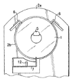
次に、発明を実施するための形態について図面を参照して詳細に説明する。図1は基板を保持する基板ホルダーの構成を示す図である。なお、図1は基板が装着された状態の基板ホルダーの正面図を示す。図1に示すように基板ホルダー2aは、基板1を装着するための基板装着孔2bと、基板装着孔2bの中で基板1を支持するための2つの固定爪6とを備えている。また、基板ホルダー2aは基板1を基板装着孔2bに装着したり、装着孔2bから取り外したりするための可動爪7と、可動爪7を駆動する可動爪駆動機構(以下、駆動機構という)12とを備えている。
Next, embodiments for carrying out the invention will be described in detail with reference to the drawings. FIG. 1 is a diagram showing a configuration of a substrate holder for holding a substrate. FIG. 1 is a front view of the substrate holder with the substrate mounted thereon. As shown in FIG. 1, the
基板1は図1に示すように中央にセンター孔を有する円盤状のハードディスク用基板でありうる。基板搬送ロボット(以下、搬送ロボットという)3の操作によりV溝を有する基板保持部5が基板1のセンター孔に挿入され、基板1は基板保持部5により鉛直姿勢で支持した状態で搬送される。本実施形態では、ハードディスク用基板を例に挙げて説明するが、本発明はこれに限ることなく、センター孔を基板保持部で支持する全ての基板の支持や搬送に使用することができる。
The
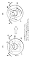
次に、図1及び図2A〜2Cを参照して搬送ロボット3により基板1を基板ホルダー2aに装着する工程を説明する。図2Aは本発明の実施形態に係る基板搬送装置により基板1を鉛直姿勢で基板カセット9から取り出す状態、図2Bは搬送ロボット3を旋回して基板1を基板ホルダー2a側に移動させた状態を示す。図2Cは基板1を基板ホルダー2aの基板装着孔2bへ渡す状態を示す。
Next, a process of mounting the
まず、図2Aに示すように搬送ロボット3は、その先端に設けられた基板保持部5を、基板カセット9に格納された基板1のセンター孔に挿入することによって、基板1を支持する。搬送ロボット3は基板1を支持したまま、図2Bに示すように基板ホルダー2aの向きに旋回することによって、基板1を移動させる。この際、図1に示す基板ホルダー2aの可動爪7は駆動機構12により押し下げられている。
First, as shown in FIG. 2A, the
次いで、図2Cに示すように搬送ロボット3は基板1を基板ホルダー2aに向けて移動させ、基板1を基板装着孔2bに挿入する。続いて、搬送ロボット3は基板1を基板装着孔2bの上側の固定爪6に押し当て、最後に駆動機構12により押し下げられている可動爪7の押し下げを解除し、可動爪7を上方に押し上げることで固定爪6と可動爪7により基板1が支持され、基板1の装着を完了する。なお、図2A〜2Cは基板の搬送工程を説明する図であるため、構造の詳細は省略している。
Next, as shown in FIG. 2C, the
図3は本発明の実施形態に係る基板支持装置の一実施形態を示す側断面図、図4は図3のX−X線における断面を分解して示す断面分解図である。図3では図1や図2A〜2Cと同一部分には同一符号を付している。本実施形態の基板支持装置は、基板ホルダー2aに基板1を装着するために搬送ロボット3により基板1を固定爪6に押し当てる時に基板1が傷付けられるのを防止するための緩衝機構を備えている。この緩衝機構は、上記特開2001−89851号公報に記載された緩衝機構を更に改良し、基板1を基板ホルダー2aに装着する際に基板1にかかる外力を軽減し、基板1への損傷や破損を確実に防止するものである。
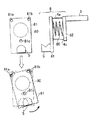
FIG. 3 is a side sectional view showing an embodiment of the substrate supporting apparatus according to the embodiment of the present invention, and FIG. 4 is an exploded sectional view showing a section taken along line XX of FIG. In FIG. 3, the same parts as those in FIG. 1 and FIGS. The substrate support apparatus of the present embodiment includes a buffer mechanism for preventing the
基板支持装置8は図3、図4に示すように第1の連結板81がV溝を有する基板保持部5に固定され、第1の連結板81に対向して第2の連結板82が配置されている。第2の連結板82は搬送ロボット3のアームの先端に固定されている。第1の連結板81と第2の連結板82とは複数の線状(紐状)の支持部材4a、4b、4cで接続され、第1、第2の連結板81、82の間には弾性を有する緩衝部材80が配置されている。
As shown in FIGS. 3 and 4, the
複数の支持部材4a、4b、4cは、同じ長さで強い強度と非弾性(又は弱弾性)を有し、第1、第2の連結板81、82の間に緩衝部材80を配置することにより、第1、第2の連結板81、82は緩衝部材80の弾性力(バネの復元力)により引っ張り力を受ける。そのため、図3に示すように、第1、第2の連結板81、82は、複数の支持部材4a、4b、4cにより、互いに離隔する方向への動きが規制され、複数の支持部材4a、4b、4cは、各々引っ張られた状態で2つの連結板81、82を接続することになり、この状態でバランスが保たれる。
The plurality of
図4に示すように第1の連結板81には第1穴81a、第2穴81b及び第3穴81cが形成され、第2の連結板82にはこれら第1穴81a、第2穴81b及び第3穴81cにそれぞれ対向して第4穴82a、第5穴82b及び第6穴82cが形成されている。第1の連結板81と第2の連結板82とは、同じ長さの線状(紐状)の第1支持部材4a、第2支持部材4b及び第3支持部材4cによって接続されている。
As shown in FIG. 4, the first connecting
即ち、第1支持部材4aの両端には、それぞれ第1の連結板81、第2の連結板82に係止される係止部が設けられている。第1支持部材4aの一端は第1の連結板81の第1穴81aに、他端は連結板82の第4穴82aに挿入され、第1支持部材4aの両端の係止部を各連結板の側面に係止させることで第1、第2の連結板81、82の間に第1支持部材4aが接続されている。
That is, locking portions that are locked to the first connecting
同様に、第2支持部材4bの両端には係止部が設けられ、第2支持部材4bの一端は連結板81の第2穴81bに、他端は連結板82の第5穴82bに挿入され、第2支持部材4bの両端に取り付けられる係止部が各連結板の側面に係止させている。この構造により第1、第2の連結板の間に第2支持部材4bが接続されている。
Similarly, locking portions are provided at both ends of the
同様に、第3支持部材4cの両端には係止部が設けられ、第3支持部材4cの一端は連結板81の第3穴81cに、他端は連結板82の第6穴82cに挿入され、第3支持部材4cの両端に取り付けられる係止部が各連結板の側面に係止させている。この構造により、第1、第2の連結板81、82の間に第3支持部材4cが接続されている。なお、基板保持部5は第1の連結板81の第1穴81a、第2穴81b及び第3穴81cを結ぶ三角形の中心に位置するように配置されている。
Similarly, locking portions are provided at both ends of the
このような第1、第2の連結板81、82を接続する線状(紐状)の支持部材や緩衝部材等を用いた支持構造は、基板1を基板ホルダーに装着する際に搬送ロボット3からの過剰な押し付け力を逃がし、基板保持部5に保持された基板1の破損や損傷を防止する。これら第1、第2の連結板81、82と少なくとも3つ以上の支持部材4a、4b、4cとの接続構造は詳しく後述する。
Such a support structure using a linear (string-like) support member, a buffer member, or the like for connecting the first and second connecting
なお、図3及び図4では第1の連結板81、第2の連結板82を設けたが、基板保持部5と第1の連結板81とを一体で構成し、搬送ロボット3と第2の連結板82とを一体で構成してもよい(例えば特許文献1の図3参照)。また、緩衝部材80としては、弾性を有する部材であれば良く、好ましくはコイルバネを好適に用いることができる。
3 and 4, the first connecting
更に、第1支持部材4a、第2支持部材4b及び第3支持部材4cは、弱弾性を有する弱弾性の部材でも良いが、好ましくは非弾性の非弾性部材を用いるのが良い。本実施形態では、例えば、多数のステンレス製ワイヤー細線を編むことにより、1本の紐状で非弾性を有する支持部材を作製している。
Further, the
この構造では、強い強度を確保できると共に自由に折り曲げ可能な紐状の非弾性の支持部材が得られる。ここで、支持部材の非弾性とは、外力を取り去ったら再び元の状態に回復しない性質を言い、この例では多数の金属細線を編むことで作製した紐状の支持部材を用いている。もちろん、支持部材は上述のように緩衝部材80の弾性力により互いに離隔する方向に力を受ける第1、第2の連結板81、82の動きを規制するものであるため、ある程度の弾性を有する弱弾性の支持部材を用いても良い。また、3つの支持部材4a、4b及び4cを用いたが、少なくとも3つ以上の支持部材があれば良い。
With this structure, it is possible to obtain a string-like inelastic support member that can ensure strong strength and can be bent freely. Here, the inelasticity of the support member means a property that does not return to the original state again when the external force is removed. In this example, a string-like support member produced by knitting a number of fine metal wires is used. Of course, since the support member regulates the movement of the first and second connecting
図5A〜5Cは第1、第2の連結板81、82を少なくとも3つ以上の線状(紐状)の支持部材で接続する構造を説明する図である。図5Aは第1の連結板81に設けられた第1穴81aの拡大斜視図である。第1の連結板81の側面には、第1支持部材4aを第1穴81aに通すための切り込み85が形成されている。
5A to 5C are diagrams illustrating a structure in which the first and second connecting
図5Bは第1の連結板81に第1支持部材4aを接続する構造を示す。第1支持部材4aを連結板81に係止するための係止部50は、ボルト状固定具52aと雌ネジ部51aから構成されている。ボルト状固定具52aの雄ネジ部は、第1の連結板81に形成された雌ネジにネジ込まれる。雌ネジ部51aはボルト状固定具52aの雄ネジ部に噛合している。ボルト状固定具52aの中央には貫通孔が形成され、更に、ボルト状固定具52aには、当該貫通孔に第1支持部材4aを通すための切り込み(不図示)が形成されている。ボルト状固定具52aは、第1の連結板81に対して軸方向に位置が調整可能であり、第1、第2の連結板81、82の間隔を調整する調整機構を備えている。
FIG. 5B shows a structure for connecting the
雌ネジ部51aにも第1支持部材4aを通すための切り込み(不図示)が形成され、雌ネジ部51aを回転させることで第1支持部材4aをボルト状固定具52aの貫通孔に通すことができる。図5Bに示すように、第1支持部材4aは、その端部に球状部(係止部)40aを有し、球状部40aがボルト状固定具52aの端部の凹部に係止して第1支持部材4aの一端を第1の連結板81に接続する構造である。なお、本実施形態では、第1支持部材4aの端部は球面状に形成したものを使用したが、本発明は、これに限定されるものではなく、例えば、すり鉢状や円錐状など他の構造でも構わない。その他の支持部材も同様である。
A cut (not shown) for passing the
このようにボルト状固定具52aの切り込み、雌ネジ51aの切り込み、第1の連結板81の側面に形成された切り込み85を揃えることにより図5Cに示すように第1支持部材4aをボルト状固定具52aの貫通孔と第1穴81aに通すことができる。第1の連結板81の第1穴81aは第1支持部材4aが移動することができる程度の直径(遊び)を有する。これは、図6Bに示すように基板1を基板装着孔2bに装着する時に基板支持装置8が撓んでも支持部材4a、4b、4cが連結板81、82の貫通孔の中である程度の移動が可能となり、基板装着動作に支障がないようにするためである。第1、第2の連結板81、82のその他の貫通穴も同様である。その後、雌ネジ部51aを第1の連結板81側に締め付けることで第1支持部材4aの接続が完了する。
Thus, the
一方、第1支持部材4aの他端にも同様に球状部(係止部)40aが形成され、第2の連結板82の側面にも第4穴82aに第1支持部材4aを通すための切り込みが形成されている。第2の連結板82には切り込みを形成するだけでボルト状固定具等は配置しなくても良い。そして、第1支持部材4aの他端側をその切り込みから第2の連結板82の第4穴82aに通すことで、第1支持部材4aの他端側の球状部(係止部)40aを第2の連結板82に係止させる。なお、第2の連結板82にも第1支持部材4aの他端側の球状部40aと係合する凹部が形成されている。
On the other hand, a spherical portion (locking portion) 40a is similarly formed at the other end of the
こうして第1支持部材4aを第1、第2の連結板81、82の間に接続することができる。第2支持部材4b及び第3支持部材4cも全く同様の構造で2つの連結板の間に接続する。その場合、第1の連結板81と第2の連結板82との間には緩衝部材80が配置されているため、その復元力により第1、第2、第3支持部材4a、4b、4cは、第1、第2の連結板81、82の間に引っ張られた状態で接続されることになる。
Thus, the
ここで、ボルト状固定具52aの位置は、上述のように、第1の連結板81に対して調整機構により軸方向に調整可能である。この調整機構により第1、第2の連結板81、82の間隔を調整し、緩衝部材80の復元力を調整可能である。もちろん、全てのボルト状固定具52aの場合も同様である。
Here, the position of the bolt-shaped
ここで、調整機構は、図5B、図5Cに示すように、ボルト状固定具52aを第1の連結板81に対してネジ機構により軸方向に進退する構造とすることができる(第1の連結板81の第1穴81aの雌ねじ部にボルト状固定具52aの雄ねじ部がネジ込まれる構造)。一方、雌ネジ部51aはボルト状固定具52aの雄ねじ部に噛合しており、雌ネジ部51aを図5Bにおいて緩める方向に回転させると、ボルト状固定具52aはフリーとなって軸方向に進退することが可能となる。
Here, as shown in FIG. 5B and FIG. 5C, the adjustment mechanism can have a structure in which the bolt-shaped
この状態で、第1の連結板81に対するボルト状固定具52aの軸方向の位置を調整する。この調整が完了すると、雌ネジ部51aを第1の連結板81側に締め付け、この状態ではボルト状固定具52aは固定された状態となり、全ての調整作業が完了する。その他のボルト状固定具52aの調整も同様である。
In this state, the axial position of the bolt-shaped
このように第1の連結板81に対してボルト状固定具52aの軸方向の位置を調整することで、第1の連結板81と第2の連結板82の距離を調整することが可能である。即ち、支持部材の一方の球状部と他方の球状部との長さは、予め定められているため、ボルト状固定具52aの雄ネジ部を緩める方向に第1の連結板81に対するボルト状固定具52aの軸方向の位置を調整すれば、第1の連結板81と第2の連結板82との距離は短くなる。逆に、ボルト状固定具52aの雄ネジ部を締める方向に第1の連結板81に対するボルト状固定具52aの軸方向の位置を調整すれば、第1の連結板81と第2の連結板82との距離は長くなる。
Thus, the distance between the first connecting
なお、ボルト状固定具52a等を含む係止部50を第1の連結板81側に配置する例を説明したが、連結板81、82のうち少なくとも一方の連結板に配置すればよい。また、第1、第2の連結板の少なくとも一方にボルト状固定具52a等を含む係止部50を配置しているが、これらボルト状固定具52a等を含む係止部50はなくても良く、第1、第2の連結板の側面に支持部材の球状部と係合する凹部を形成しておいても良い。但し、図3に示す基板支持装置は、第1、第2の連結板81、82の両方にボルト状固定具52a等を含む係止部50を配置した例を示す。
In addition, although the example which arrange | positions the latching | locking
次に、図6A、6B及び図7A、7Bを参照して本発明の実施形態に係る基板支持装置を用いて基板1を基板ホルダー2aに装着する動作を説明する。図6Aは搬送ロボット3で基板1を基板ホルダー2a側に移動させた状態を示す。図6Bは基板1を基板ホルダー2aの基板装着孔2bへ受け渡す状態を示す。
Next, with reference to FIGS. 6A and 6B and FIGS. 7A and 7B, an operation of mounting the
図7A、7Bは本発明の実施形態に係る基板支持装置により基板ホルダー2aの固定爪6に基板1を押し当てる動作を説明する図である。図6A、6B、図7A、7Bでは図1乃至図4と同一部分には同一符号を付している。
7A and 7B are views for explaining the operation of pressing the
まず、上述のように搬送ロボット3により基板カセット9から基板1を取り出し、基板1を鉛直姿勢で基板保持部5に保持した状態で、図6Aに示すように搬送ロボット3により基板1を基板ホルダー2a側に移動させる。ここまでは、図2A、図2Bの説明と同様である。
First, the
次いで、図6Bに示すように搬送ロボット3により基板保持部5に鉛直姿勢で保持された基板1を基板装着孔2bへ挿入し、その後、基板1を基板保持部材5で支持した状態で持ち上げ、基板1の外周を基板装着孔2b内の固定爪6に押し付ける。この時、駆動機構12により可動爪7は押し下げられている。その際、図7Aに示すように2個の固定爪6に基板1が同時に当たらなかった場合、2個の固定爪6のうち片方の固定爪6に当たっている状態で基板1を固定爪6に押し当てると、図7Bに示すように基板保持部5が矢印方向に回転する。
Next, as shown in FIG. 6B, the
つまり、2つの連結板81、82は3つ以上の支持部材4a、4b、4cで接続され、2つの連結板81、82の間に緩衝部材80が配置されているため、先に当った固定爪6と基板1との接触点を支点に基板保持部5が回転し、基板1が回転し又は横方向に動くことになる。緩衝部材80は上下方向だけでなく左右方向或いはネジレに対して弾性機能を備えているため、基板1は適度な力で2つの固定爪6に押し付けられ、基板1の外周面に傷を付けることがない。即ち、基板1にかかる外力が低減され、固定爪6より柔らかい基板であっても基板への損傷や破損を防止でき、安定して基板1を基板ホルダー2aに装着することが可能となる。
That is, the two connecting
基板1が基板装着孔2b内で2つの固定爪6に押し当てられると、駆動機構12により押し下げられていた可動爪7が解除され、図6Bに示すように可動爪7は矢印方向に可動して基板1を下方向から支持する。このようにして基板1は基板装着孔2b内で2つの固定爪6と1つの可動爪7によって支持され、基板1の基板ホルダー2aへの装着が完了する。
When the
本実施形態では、上述のように基板1にかかる外力を低減できるため、基板の損傷や破損を確実に防止することができる。そのため、高スループットで成膜処理等を行えるばかりでなく、基板を受け渡す位置精度及び基板支持爪の弾性や材質の許容範囲を広くすることができる。更に、基板支持装置を複数連結することも可能となる。また、緩衝部材80等の機構により高温プロセスによる基板ホルダーの熱膨張や加工・組立による誤差を吸収できるため、基板の受け渡しの精密な位置調整が不要となり、簡単に搬送機構の調整を行うことが可能となる。
In this embodiment, since the external force applied to the
なお、上述の実施形態では、第1の連結板81において第1穴81a、第2穴81b及び第3穴81cを結ぶ三角形の中心に位置するように基板保持部5を設けたが、図8に示すように、第3穴81cの下方に位置するように基板保持部5を設けてもよい。こうすることで、搬送ロボットによって、上述した実施形態と同じ回転角だけ回転しても、基板保持部5の移動量を大きくすることができ、ロボットによる少ない回転で基板の片当りを容易に補正することができる。
In the above-described embodiment, the
以下、本発明の実施形態にかかる電気デバイスの製造装置及び電気デバイスの製造方法によって製造される電気デバイスの一例である磁気記録媒体について説明する。なお、本明細書において、「磁気記録媒体」という用語は、情報の記録、読み取りに磁気のみを用いるハードディスク、フロッピー(登録商標)ディスク等の光ディスク等に限定されない。例えば、磁気と光を併用するMO(Magneto Optical)等の光磁気記録媒体、磁気と熱を併用する熱アシスト型の記録媒体も含むものとする。 Hereinafter, a magnetic recording medium which is an example of an electric device manufactured by an electric device manufacturing apparatus and an electric device manufacturing method according to an embodiment of the present invention will be described. In this specification, the term “magnetic recording medium” is not limited to a hard disk that uses only magnetism for recording and reading information, an optical disk such as a floppy (registered trademark) disk, and the like. For example, a magneto-optical recording medium such as MO (Magneto Optical) using both magnetism and light, and a heat-assisted recording medium using both magnetism and heat are also included.
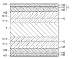
図9は、本発明の実施形態にかかる磁気記録媒体の製造装置及び磁気記録媒体の製造方法によって製造される磁気記録媒体(薄膜積層体)の一例を示す模式的な断面図である。本実施形態においては、磁気記録媒体として、垂直記録媒体に改良を加えたECC(Exchange−coupled composite)媒体を例示的に説明するが、本発明の趣旨はこの例に限定されない。例えば、一般的な垂直記録媒体、長手記録媒体、ビットパターンドメディア、熱アシスト型の記録媒体であってもよい。 FIG. 9 is a schematic cross-sectional view showing an example of a magnetic recording medium (thin film laminate) manufactured by the magnetic recording medium manufacturing apparatus and the magnetic recording medium manufacturing method according to the embodiment of the present invention. In this embodiment, an ECC (Exchange-Coupled Composite) medium obtained by improving a perpendicular recording medium will be described as an example of the magnetic recording medium. However, the gist of the present invention is not limited to this example. For example, a general perpendicular recording medium, a longitudinal recording medium, a bit patterned medium, and a heat-assisted recording medium may be used.
図9に示すように、磁気記録媒体は、例えば、基板1と、基板1の両面又は片面上に順次積層された第1軟磁性層101aと、スペーサー層102と、第2軟磁性層101bと、シード層103と、磁性層104と、交換結合制御層105と、第3軟磁性層106と、保護層107とから構成されている。
As shown in FIG. 9, the magnetic recording medium includes, for example, a
基板1の材料としては、磁気記録媒体用基板として一般的に用いられているガラス、NiPメッキ膜が形成されたAl合金、セラミックス、可曉性樹脂、Si等の非磁性材料を用いることができる。本実施形態における基板1は、中心に孔を有する円板状部材であるが、これに限定されるものではなく、例えば、矩形部材であってもよい。
As a material of the
基板1の上に形成される第1軟磁性層101aは、磁気記録に用いる磁気ヘッドからの磁束を制御して記録・再生特性を向上するために形成される層であるが、省略することもできる。第1軟磁性層101aの構成材料としては、例えば、CoZrNb、CoZrTa、FeCoBCrを直上の膜に合わせて使用することができる。
The first soft
スペーサー層102の材料としては、例えば、Ru、及びCrを使用することができる。スペーサー層102の上に形成される第2軟磁性層101bは、第1軟磁性層101aと同様である。第1軟磁性層101a、スペーサー層102、及び第2軟磁性層101bにより、軟磁性下地膜(Soft underlayer)が構成される。
As a material of the
軟磁性下地膜の上に形成されているシード層103は、磁性層104の結晶配向性、結晶粒径、粒径分布、粒界偏析を好適に制御するために磁性層104の直下に形成される層である。シード層103の材料としては、例えば、MgO、Cr、Ru、Pt,及びPdを使用することができる。
The
磁気記録層5は、Ku値の大きな磁性層104と、交換結合制御層105と、Ku値の小さな第3軟磁性層106とを含む。
The
シード層103の上に形成されている、Ku値の大きな磁性層104は、磁気記録層5の全体のKu値を担う層であり、Ku値ができるだけ大きい材料を使用する。磁性層104の材料としては、磁化容易軸が基板面に対して垂直な材料であって、強磁性粒子が酸化物の非磁性粒界成分によって分離された構造であるものを使用することができる。例えば、CoPtCr−SiO2、CoPt−SiO2など、少なくともCoPtを含む強磁性材料に、酸化物を添加したものを使用することができる。また、他の材料として、Co50Pt50、Fe50Pt50、及びCo50−yFeyPt50を使用してもよい。
The
磁性層104の上に形成されている交換結合制御層105は、結晶質の金属若しくは合金と、酸化物とを含む。結晶質の金属或いは合金の材料としては、例えば、Pt、Pd、或いはそれらの合金を使用することができる。また、結晶質の合金としては、例えば、Co、Ni、Feから選ばれた元素と非磁性の金属との合金も使用することができる。
The exchange
磁性層104と第3軟磁性層106との交換結合力の強さは、交換結合制御層105の膜厚を変化させることにより、最も簡単に制御することができる。交換結合制御層105の膜厚は、例えば、0.5〜2.0nmとする。
The strength of the exchange coupling force between the
交換結合制御層105の上に形成されている第3軟磁性層106は、磁化反転磁界を低減させる役割を主に担うため、Ku値ができるだけ小さい材料を使用する。第3軟磁性層106の材料としては、例えば、Co、NiFe、及びCoNiFeを使用することができる。
Since the third soft
第3軟磁性層106の上に形成されている保護層107は、ヘッドと媒体表面の接触による損傷を防ぐために形成される。保護層107の材料としては、例えば、C、SiO2、ZrO2等の単一成分またはそれぞれを主成分とし、これに添加元素を含有させたものを使用することができる。
The
次に、本発明の実施形態にかかる磁気記録媒体の製造方法で用いる薄膜形成装置(以下、「磁気記録媒体製造装置」ともいう)について説明する。図10は、本発明の実施形態にかかる磁気記録媒体製造装置の一例を示す模式図である。 Next, a thin film forming apparatus (hereinafter also referred to as “magnetic recording medium manufacturing apparatus”) used in the method for manufacturing a magnetic recording medium according to an embodiment of the present invention will be described. FIG. 10 is a schematic diagram showing an example of a magnetic recording medium manufacturing apparatus according to an embodiment of the present invention.
図10に示すように、磁気記録媒体製造装置においては、キャリア2に基板1(図9)を搭載するためのロードロックチャンバ810、キャリア2から基板1の回収を行うためのアンロードロックチャンバ820、複数のチャンバ201、202、203、204、205、206、207、208、209、210、211、212、213、214、215、216、217、218が方形の輪郭に沿って配置されている。また、ロードロックチャンバ810、チャンバ201〜218、アンロードロックチャンバ820に沿って搬送路が形成されている。搬送路には、基板1を搭載可能な、複数のキャリア2が設けられている。各チャンバにおいて基板1の処理に要する処理時間(タクトタイム)は、予め決められており、この処理時間(タクトタイム)が経過すると、キャリア2に搭載された基板1が、順次、次のチャンバに搬送されるように構成されている。
As shown in FIG. 10, in the magnetic recording medium manufacturing apparatus, a
なお、キャリア2は、複数のチャンバ間に渡って基板ホルダー2aを搬送する搬送機構を備えている。図1に示すように、基板ホルダー2aは、基板1を装着するための基板装着孔2bと、基板装着孔2bに基板1を支持するための2つの固定爪6とを含む。
The
磁気記録媒体製造装置が1時間あたり約1000枚の基板を処理するためには、1つのチャンバにおけるタクトタイムは、約5秒以下、望ましくは約3.6秒以下となる。 In order for the magnetic recording medium manufacturing apparatus to process about 1000 substrates per hour, the tact time in one chamber is about 5 seconds or less, preferably about 3.6 seconds or less.
ロードロックチャンバ810、アンロードロックチャンバ820、チャンバ201、202、203、204、205、206、207、208、209、210、211、212、213、214、215、216、217、218の各々は、専用又は兼用の排気系によって排気可能な真空チャンバである。ロードロックチャンバ810、アンロードロックチャンバ820、チャンバ201、202、203、204、205、206、207、208、209、210、211、212、213、214、215、216、217、218の各々の境界部分には、ゲートバルブ(不図示)が設けられている。
Each of the
なお、ロードロックチャンバ810及びアンロードロックチャンバ820には、それぞれ基板保持部5を有する搬送ロボット3が設けられている。
Each of the
具体的には、磁気記録媒体製造装置のチャンバ201は、基板1に第1軟磁性層101aを形成するためのチャンバである。方向転換チャンバ202は、キャリア2の搬送方向を転換するためのチャンバである。チャンバ203は、第1軟磁性層101aの上にスペーサー層102を形成するためのチャンバである。チャンバ204は、スペーサー層102の上に第2軟磁性層101bを形成するためのチャンバである。チャンバ205は、第2軟磁性層101bの上にシード層103を形成するためのチャンバである。方向転換チャンバ206は、キャリア2の搬送方向を転換するためのチャンバである。チャンバ207(第1加熱チャンバ)及びチャンバ208(第2加熱チャンバ)は、基板1を予め加熱するためのプレヒート用のチャンバである。なお、チャンバ209において、シード層103を形成することも可能である。
Specifically, the
チャンバ210及び211は、シード層103の上に磁性層104を形成するためのスパッタ装置として機能することが可能なチャンバである。方向転換チャンバ212は、キャリア2の方向を転換するためのチャンバである。冷却チャンバ213は、基板1を冷却するためのチャンバである。チャンバ214は、磁性層104の上に交換結合制御層105を形成するためのチャンバである。チャンバ215は、交換結合制御層105の上に第3軟磁性層106を形成するためのチャンバである。方向転換チャンバ216は、キャリア2の方向を転換するためのチャンバである。チャンバ217、及び218は、保護層107を形成するためのチャンバである。
The
次に、図9、図11を参照して、本発明の実施形態にかかる磁気記録媒体製造装置を用いた磁気記録媒体の製造方法について説明する。 Next, a method for manufacturing a magnetic recording medium using the magnetic recording medium manufacturing apparatus according to the embodiment of the present invention will be described with reference to FIGS.
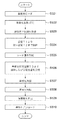
ステップS501において、ロードロックチャンバ810に基板を搬入し、図3に示す搬送ロボット3により、基板1をキャリア2に搭載して基板をロードする。ここで、ロードロックチャンバ810は、前述したように、搬送ロボット3により基板1を固定爪6に押し当てる時に基板1が傷付けられるのを防止するための緩衝機構を備えているため、基板1を基板ホルダー2aに装着する際に基板1にかかる外力を軽減し、基板1への損傷や破損を確実に防止することができる。
In step S501, the substrate is loaded into the
次にステップS502において、ロードロックチャンバ810内で、基板に付着した汚染物質や水分を取り除くため、基板を所定の温度T1(約100度)まで加熱する。
Next, in step S502, the substrate is heated to a predetermined temperature T1 (about 100 degrees) in the
ステップS503において、軟磁性下地膜(Soft underlayer)を形成する。具体的には、チャンバ201で第1軟磁性層101aを形成し、チャンバ203でスペーサー層102(厚さは0.7〜2nm)を形成し、チャンバ204で第2軟磁性層101bを形成する。
In step S503, a soft underlayer is formed. Specifically, the first soft
ステップS504においては、チャンバ207(第1加熱チャンバ)及びチャンバ208(第2加熱チャンバ)に基板を順次搬送して、ステップS502で加熱された温度T1(約100度)より高い温度T2(約400℃〜700℃)まで、基板を加熱する。これは、この後、磁性層104を形成する際に、磁気記録層5の磁気異方性を高めるための準備工程である。磁気記録媒体製造装置において、スループットの向上のため、一つのチャンバ内の処理時間(タクトタイム)は制限されている。この限られた時間内に、磁性層104を形成するためのチャンバ210、211において、磁性層104の磁気異方性を高めるために必要な温度まで、加熱するのは難しい。そのため、磁気記録媒体製造装置は、プレヒート(予備加熱)用として、チャンバ207(第1加熱チャンバ)及びチャンバ208(第2加熱チャンバ)とを備えている。磁気記録媒体製造装置において、チャンバ207(第1加熱チャンバ)及びチャンバ208(第2加熱チャンバ)は、予備加熱器として機能する。
In step S504, the substrate is sequentially transferred to the chamber 207 (first heating chamber) and the chamber 208 (second heating chamber), and the temperature T2 (about 400 degrees) higher than the temperature T1 (about 100 degrees) heated in step S502. The substrate is heated up to a temperature of from 700C to 700C. This is a preparatory step for increasing the magnetic anisotropy of the
磁性層104を形成するためのチャンバ210まで基板を搬送するまでに、基板の温度が低下してしまうことを考慮して、チャンバ207(第1加熱チャンバ)及びチャンバ208(第2加熱チャンバ)では、チャンバ210で磁気異方性を高めるために必要な温度以上に加熱(予備加熱)しておく必要がある。しかし、加熱しすぎると、ガラス製の基板は、塑性変形を起こし、基板がキャリア2から落下するなどの問題を引き起こす危険性がある。そのため、チャンバ207(第1加熱チャンバ)及びチャンバ208(第2加熱チャンバ)では、ガラス製の基板が塑性変形を起こさない程度の温度、例えば600℃、までの加熱する。
Considering that the temperature of the substrate decreases before the substrate is transferred to the
ステップS505において、磁性層104の結晶特性を好適に制御するため、シード層103を形成する。なお、シード層103の形成は、ステップS504の加熱工程の前に、チャンバ205で行ってもよい。
In step S505, the
ステップS506において、磁性層104を形成するためのチャンバ210、211に基板を搬送して、基板を所定の温度T3(約400℃〜600℃)まで加熱しながら磁性層104を形成する。ここでは、前述したようにチャンバ210において、基板を均一に加熱しながら磁性層104の形成を行う。
In step S506, the substrate is transferred to
ステップS507において、冷却チャンバ213に基板を順次搬送して、保護層107の形成に最適な温度まで、基板を冷却する。保護層107の材料としてカーボンを使用する場合、例えば、約200℃以下まで、基板を冷却する必要がある。
In step S <b> 507, the substrate is sequentially transferred to the
その後、ステップS508において、搬送ロボット3を備えたチャンバ216にキャリアを搬送して、図7や図8で説明したように、基板1を回転させる。ここで、チャンバ216は、前述したように、搬送ロボット3により基板1を固定爪6に押し当てる時に基板1が傷付けられるのを防止するための緩衝機構を備えているため、基板1を基板ホルダー2aから取り外して回転する際に基板1にかかる外力を軽減し、基板1への損傷や破損を確実に防止することができる。
Thereafter, in step S508, the carrier is transferred to the
その後、ステップS509において、CVD用のチャンバ217及びチャンバ218に基板を搬送して、CVD法により、保護層107を形成する。
Thereafter, in step S509, the substrate is transferred to the
なお、磁性層104と保護層107との間に、チャンバ214で極薄の交換結合制御層105を形成してもよい。また、基板を冷却した後で、かつ保護層107を形成する前に、チャンバ215において第3軟磁性層106を形成してもよい。
Note that an ultrathin exchange
そして、ステップS510において、アンロードロックチャンバ820において、キャリア2から基板を取り外し、基板をアンロードする。ここで、アンロードロックチャンバ820は、前述したように、搬送ロボット3により基板1を固定爪6に押し当てる時に基板1が傷付けられるのを防止するための緩衝機構を備えているため、基板1を基板ホルダー2aから取り外す際に基板1にかかる外力を軽減し、基板1への損傷や破損を確実に防止することができる。
In step S510, in the unload
1 基板
2a 基板ホルダー
2b 基板装着孔
3 搬送ロボット
4a 第1支持部材
4b 第2支持部材
4c 第3支持部材
5 基板保持部
6 固定爪
7 可動爪
8 基板支持装置
9 基板カセット
12 駆動機構
40a 球状部(係止部)
50 係止部
51a 雌ネジ部
52a ボルト状固定具
80 緩衝部材
81 第1の連結板
81a、81b、81c 第1穴、第2穴、第3穴
82 第2の連結板
82a、82b、82c 第4穴、第5穴、第6穴
85 切り込み
2 キャリア
810 ロードロックチャンバ
820 アンロードロックチャンバ
100 基板
101a 第1軟磁性層
102 スペーサー層
101b 第2軟磁性層
103 シード層
104 磁性膜
105 交換結合制御層
106 第3軟磁性層
107 保護膜
201〜218 チャンバ
DESCRIPTION OF
50
Claims (9)
前記基板保持部に連結された第1の連結板と、
前記第1の連結板に対向して配置され、前記基板を基板ホルダーに搬送する搬送ロボットに連結される第2の連結板と、
前記第2の連結板に対して前記第1の連結板が水平方向及び重力方向に移動することができるように前記第1の連結板と前記第2の連結板との間に配置された緩衝部材と、
前記第1の連結板と前記第2の連結板とが互いに離間する方向へ動くことを規制する支持部材と、を備え、
前記支持部材は、前記緩衝部材の復元力によって引っ張られた状態で、前記第1の連結板と前記第2の連結板との間に配置されていることを特徴とする基板支持装置。 A substrate support device for inserting a substrate holding portion into a center hole provided in the substrate, and supporting the substrate in a vertical posture by the substrate holding portion,
A first connecting plate connected to the substrate holder;
A second connecting plate disposed opposite to the first connecting plate and connected to a transfer robot for transferring the substrate to a substrate holder;
A buffer disposed between the first connecting plate and the second connecting plate so that the first connecting plate can move in a horizontal direction and a gravitational direction with respect to the second connecting plate. Members,
And a supporting member for restricting said first connecting plate and the second connecting plate move away from each other,
Said support member, said in a state of being pulled by the restoring force of the cushioning member, the substrate supporting device, characterized that you have been arranged between the first connecting plate and the second connecting plate.
前記第1の連結板、前記第2の連結板、前記ボルト状固定具及び前記雌ネジ部の切り込みを合わせることで、前記支持部材が前記第1の連結板および前記第2の連結板の貫通孔及び前記ボルト状固定具の貫通孔に挿入されていることを特徴とする請求項5に記載の基板支持装置。 A bolt-shaped fixture having a through hole and a notch for inserting the support member into the through-hole in at least one of the first coupling plate and the second coupling plate, and a male thread portion of the bolt-shaped fixture And an internal thread portion having a notch that meshes with
By aligning the notches of the first connecting plate, the second connecting plate, the bolt-shaped fixture, and the female screw portion, the support member penetrates the first connecting plate and the second connecting plate. The substrate support device according to claim 5 , wherein the substrate support device is inserted into a hole and a through hole of the bolt-shaped fixture.
前記搬送ロボットにより前記基板支持装置の前記基板保持部で支持された前記基板を前記基板装着孔に挿入し、且つ、前記基板を前記固定爪に押し当て、前記基板が前記固定爪に押し当てられた後、前記可動爪を前記基板に押し当てることによって前記基板が前記基板ホルダーの前記基板装着孔に装着されることを特徴とする請求項7に記載の基板搬送装置。 The substrate holder is provided with a substrate mounting hole for mounting the substrate, the substrate mounting hole is provided with a fixed claw for supporting the substrate and a movable claw for mounting or removing the substrate,
The substrate supported by the substrate holding part of the substrate support device is inserted into the substrate mounting hole by the transfer robot, and the substrate is pressed against the fixed claw, and the substrate is pressed against the fixed claw. The substrate transfer apparatus according to claim 7 , wherein after the movable claw is pressed against the substrate, the substrate is mounted in the substrate mounting hole of the substrate holder.
前記基板搬送装置は、基板支持装置および搬送ロボットを含み、基板を基板ホルダーに搬送するように構成され、
前記基板支持装置は、前記基板に設けられたセンター孔に基板保持部を挿入し、前記基板保持部で前記基板を鉛直姿勢で支持するように構成され、かつ、前記基板保持部に連結された第1の連結板と、
前記第1の連結板に対向して配置され、前記搬送ロボットに連結される第2の連結板と、
前記第2の連結板に対して前記第1の連結板が水平方向及び重力方向に移動することができるように前記第1の連結板と前記第2の連結板との間に配置された緩衝部材と、
前記第1の連結板と前記第2の連結板とが互いに離間する方向へ動くことを規制するために、前記緩衝部材の復元力によって引っ張られた状態で、前記第1の連結板と前記第2の連結板との間に配置された支持部材とを含み、
前記キャリアは、前記基板ホルダーを保持して前記複数のチャンバ間を搬送するように構成され、
前記製造方法は、
前記基板搬送装置から前記キャリアに基板を搬送する工程と、
前記キャリアを前記成膜チャンバに搬送して、前記基板に成膜を行なう工程を含む、ことを特徴とする製造方法。 A manufacturing method for manufacturing an electrical device using a substrate transport apparatus, a plurality of chambers including at least one film forming chamber, and a manufacturing apparatus including a carrier,
The substrate transfer device includes a substrate support device and a transfer robot, and is configured to transfer a substrate to a substrate holder,
The substrate support device is configured to insert a substrate holding portion into a center hole provided in the substrate, and to support the substrate in a vertical posture by the substrate holding portion, and is connected to the substrate holding portion. A first connecting plate;
A second connecting plate disposed opposite to the first connecting plate and connected to the transfer robot;
A buffer disposed between the first connecting plate and the second connecting plate so that the first connecting plate can move in a horizontal direction and a gravitational direction with respect to the second connecting plate. Members,
To regulate said first connecting plate and the second connecting plate move away from each other, in a state of being pulled by the restoring force of the cushioning member, wherein said first connecting plate first A support member disposed between the two connecting plates ,
The carrier is configured to convey the plurality of chambers while holding the substrate holder,
The manufacturing method includes:
Transporting a substrate from the substrate transport apparatus to the carrier;
A manufacturing method comprising the steps of transporting the carrier to the film forming chamber and forming a film on the substrate.
Priority Applications (3)
| Application Number | Priority Date | Filing Date | Title |
|---|---|---|---|
| JP2010020734A JP5457216B2 (en) | 2009-02-27 | 2010-02-01 | Substrate support apparatus, substrate transfer apparatus, and electrical device manufacturing method |
| US12/706,901 US8770906B2 (en) | 2009-02-27 | 2010-02-17 | Substrate support apparatus and substrate transport apparatus having shock absorption |
| CN201010126048.9A CN101901603A (en) | 2009-02-27 | 2010-02-26 | Substrate support apparatus, substrate transport apparatus, and electrical device manufacturing method |
Applications Claiming Priority (3)
| Application Number | Priority Date | Filing Date | Title |
|---|---|---|---|
| JP2009045597 | 2009-02-27 | ||
| JP2009045597 | 2009-02-27 | ||
| JP2010020734A JP5457216B2 (en) | 2009-02-27 | 2010-02-01 | Substrate support apparatus, substrate transfer apparatus, and electrical device manufacturing method |
Publications (3)
| Publication Number | Publication Date |
|---|---|
| JP2010222700A JP2010222700A (en) | 2010-10-07 |
| JP2010222700A5 JP2010222700A5 (en) | 2013-03-14 |
| JP5457216B2 true JP5457216B2 (en) | 2014-04-02 |
Family
ID=42667178
Family Applications (1)
| Application Number | Title | Priority Date | Filing Date |
|---|---|---|---|
| JP2010020734A Active JP5457216B2 (en) | 2009-02-27 | 2010-02-01 | Substrate support apparatus, substrate transfer apparatus, and electrical device manufacturing method |
Country Status (3)
| Country | Link |
|---|---|
| US (1) | US8770906B2 (en) |
| JP (1) | JP5457216B2 (en) |
| CN (1) | CN101901603A (en) |
Families Citing this family (3)
| Publication number | Priority date | Publication date | Assignee | Title |
|---|---|---|---|---|
| US9070730B2 (en) * | 2011-10-07 | 2015-06-30 | Varian Semiconductor Equipment Associates, Inc. | Method and apparatus for removing a vertically-oriented substrate from a cassette |
| JP5892783B2 (en) * | 2011-12-21 | 2016-03-23 | キヤノンアネルバ株式会社 | Substrate support device and substrate transfer device |
| CN113066742B (en) * | 2021-03-18 | 2023-11-10 | 浙江芯能光伏科技股份有限公司 | Automatic conveying equipment for producing solar polycrystalline silicon wafers |
Family Cites Families (10)
| Publication number | Priority date | Publication date | Assignee | Title |
|---|---|---|---|---|
| US4086870A (en) * | 1977-06-30 | 1978-05-02 | International Business Machines Corporation | Novel resist spinning head |
| US5457368A (en) * | 1993-03-09 | 1995-10-10 | University Of Utah Research Foundation | Mechanical/electrical displacement transducer |
| JPH07278820A (en) * | 1994-04-13 | 1995-10-24 | Anelva Corp | Supporting mechanism for substrate heating holder |
| US5851041A (en) * | 1996-06-26 | 1998-12-22 | Ontrak Systems, Inc. | Wafer holder with spindle assembly and wafer holder actuator |
| TW484184B (en) * | 1998-11-06 | 2002-04-21 | Canon Kk | Sample separating apparatus and method, and substrate manufacturing method |
| JP4365920B2 (en) * | 1999-02-02 | 2009-11-18 | キヤノン株式会社 | Separation method and semiconductor substrate manufacturing method |
| JP4307653B2 (en) * | 1999-09-17 | 2009-08-05 | キヤノンアネルバ株式会社 | Substrate support device and substrate transfer mechanism |
| DE19962170A1 (en) * | 1999-12-22 | 2001-07-12 | Steag Micro Tech Gmbh | Sub-beam holder |
| JP2001216689A (en) * | 2000-01-31 | 2001-08-10 | Anelva Corp | Substrate supporting mechanism and substrate supporting /rotating device |
| US20040177813A1 (en) * | 2003-03-12 | 2004-09-16 | Applied Materials, Inc. | Substrate support lift mechanism |
-
2010
- 2010-02-01 JP JP2010020734A patent/JP5457216B2/en active Active
- 2010-02-17 US US12/706,901 patent/US8770906B2/en active Active
- 2010-02-26 CN CN201010126048.9A patent/CN101901603A/en active Pending
Also Published As
| Publication number | Publication date |
|---|---|
| US20100221089A1 (en) | 2010-09-02 |
| JP2010222700A (en) | 2010-10-07 |
| US8770906B2 (en) | 2014-07-08 |
| CN101901603A (en) | 2010-12-01 |
Similar Documents
| Publication | Publication Date | Title |
|---|---|---|
| US11804242B2 (en) | Reader noise reduction using spin hall effects | |
| US8467148B2 (en) | Spin torque oscillator, magnetic recording head, magnetic head assembly and magnetic recording apparatus | |
| US7274538B2 (en) | Sensor with semi-permanently deformable element for active element adjustment | |
| US9728218B2 (en) | Magnetic recording medium for heat-assisted magnetic recording | |
| JP5529484B2 (en) | Substrate transport apparatus and magnetic recording medium manufacturing method | |
| US9093099B2 (en) | Perpendicular magnetic recording medium and method for manufacturing the same | |
| SG183737A1 (en) | Single-sided perpendicular magnetic recording medium | |
| JP5457216B2 (en) | Substrate support apparatus, substrate transfer apparatus, and electrical device manufacturing method | |
| US10311901B1 (en) | Anisotropy field induced self pinned recessed antiferromagnetic reader | |
| JP6303167B2 (en) | In-line film forming apparatus and method for manufacturing magnetic recording medium using the same | |
| JP2010106349A (en) | Sputtering device, thin-film-forming apparatus, and method for manufacturing magnetic recording medium | |
| US20100006420A1 (en) | Inline interlayer heater apparatus | |
| JP5336151B2 (en) | Thin film forming apparatus and method of manufacturing magnetic recording medium | |
| US9824711B1 (en) | Soft underlayer for heat assisted magnetic recording media | |
| US9984713B1 (en) | Heat assisted magnetic recording media with enhanced tuning exchange coupling | |
| US20080261081A1 (en) | Perpendicular magnetic recording medium and method of manufacturing the same | |
| Shams et al. | C-axis oriented Ba-ferrite thin film with perpendicular anisotropy deposited on Si/sub 3/N/sub 4/substrate | |
| US8208238B1 (en) | Apparatus for orienting soft-underlayer deposition | |
| JP5371731B2 (en) | Film forming method, substrate rotating apparatus, and vacuum processing apparatus | |
| US9343273B2 (en) | Substrate holders for uniform reactive sputtering | |
| JP5492453B2 (en) | Method for manufacturing magnetic recording medium | |
| JP2009289383A (en) | Manufacturing method of magnetic recording medium, and magnetic recording medium | |
| JP2007066477A (en) | Perpendicular magnetic recording medium and perpendicular magnetic recording device |
Legal Events
| Date | Code | Title | Description |
|---|---|---|---|
| A621 | Written request for application examination |
Free format text: JAPANESE INTERMEDIATE CODE: A621 Effective date: 20130116 |
|
| A521 | Request for written amendment filed |
Free format text: JAPANESE INTERMEDIATE CODE: A523 Effective date: 20130125 |
|
| A977 | Report on retrieval |
Free format text: JAPANESE INTERMEDIATE CODE: A971007 Effective date: 20130930 |
|
| A131 | Notification of reasons for refusal |
Free format text: JAPANESE INTERMEDIATE CODE: A131 Effective date: 20131004 |
|
| A521 | Request for written amendment filed |
Free format text: JAPANESE INTERMEDIATE CODE: A523 Effective date: 20131119 |
|
| TRDD | Decision of grant or rejection written | ||
| A01 | Written decision to grant a patent or to grant a registration (utility model) |
Free format text: JAPANESE INTERMEDIATE CODE: A01 Effective date: 20131220 |
|
| A61 | First payment of annual fees (during grant procedure) |
Free format text: JAPANESE INTERMEDIATE CODE: A61 Effective date: 20140109 |
|
| R150 | Certificate of patent or registration of utility model |
Ref document number: 5457216 Country of ref document: JP Free format text: JAPANESE INTERMEDIATE CODE: R150 |
|
| R250 | Receipt of annual fees |
Free format text: JAPANESE INTERMEDIATE CODE: R250 |
|
| R250 | Receipt of annual fees |
Free format text: JAPANESE INTERMEDIATE CODE: R250 |
|
| R250 | Receipt of annual fees |
Free format text: JAPANESE INTERMEDIATE CODE: R250 |
|
| R250 | Receipt of annual fees |
Free format text: JAPANESE INTERMEDIATE CODE: R250 |
|
| R250 | Receipt of annual fees |
Free format text: JAPANESE INTERMEDIATE CODE: R250 |
|
| R250 | Receipt of annual fees |
Free format text: JAPANESE INTERMEDIATE CODE: R250 |
|
| R250 | Receipt of annual fees |
Free format text: JAPANESE INTERMEDIATE CODE: R250 |
|
| R250 | Receipt of annual fees |
Free format text: JAPANESE INTERMEDIATE CODE: R250 |