JP5452190B2 - Current sensor and assembly method thereof - Google Patents
Current sensor and assembly method thereof Download PDFInfo
- Publication number
- JP5452190B2 JP5452190B2 JP2009271585A JP2009271585A JP5452190B2 JP 5452190 B2 JP5452190 B2 JP 5452190B2 JP 2009271585 A JP2009271585 A JP 2009271585A JP 2009271585 A JP2009271585 A JP 2009271585A JP 5452190 B2 JP5452190 B2 JP 5452190B2
- Authority
- JP
- Japan
- Prior art keywords
- case member
- main body
- body case
- magnetic
- fitting
- Prior art date
- Legal status (The legal status is an assumption and is not a legal conclusion. Google has not performed a legal analysis and makes no representation as to the accuracy of the status listed.)
- Active
Links
Images


Description
本発明は、電流センサ及びその組立方法に関し、より詳細には、電気機器を対象とする安全規格を考慮しつつ沿面距離の確保と、小型化や小占有面積化を図るように容易な組立を可能にした電流センサ及びその組立方法に関する。 The present invention relates to a current sensor and a method for assembling the current sensor. More particularly, the present invention relates to a current sensor and a method for assembling the current sensor. The present invention relates to an enabled current sensor and an assembling method thereof.
従来の電流センサは、産業用の汎用インバータやモータ制御機器、またはそのような機器内に配線された被測定電流導体に流れる電流を検出するために、略コ字状のコアと、このコアのギャップ部に配置された磁気センサとを備え、これらのコアや磁気センサなどの全体を絶縁樹脂で被覆して一体化を図り、磁気センサによりコアに生じる磁束変化を電流として検出するものが知られている(例えば、特許文献1参照)。 A conventional current sensor has a generally U-shaped core and a core of this core in order to detect a current flowing in a general-purpose inverter for industrial use, a motor control device, or a current conductor to be measured wired in such a device. It has a magnetic sensor arranged in the gap part, and these cores and magnetic sensors are covered with insulating resin to integrate them, and the magnetic sensor detects changes in magnetic flux generated in the core as current. (For example, refer to Patent Document 1).
また、これらのコアや磁気センサなどをケース部材や蓋部材によって挟持固定するためにコアや磁気センサなどを樹脂モールドして一体化したものも知られている(例えば、特許文献2参照)。 In addition, in order to sandwich and fix these cores, magnetic sensors, and the like with case members and lid members, a core, magnetic sensor, and the like are integrated by resin molding (see, for example, Patent Document 2).
近年、電流センサの小型化や薄型化を図るために、電気機器を対象とする安全規格を考慮しつつ、空間距離や沿面距離に着目した製品開発が求められている。電気部品要素を絶縁物で隔離することなく電気的絶縁を達成するためには、空間距離及び沿面距離(Clearance and Creepage Distance)の双方を確保する必要がある。空間距離(clearance)とは、2つの導電性部分間の空間を通る最短距離であり、沿面距離(creepage distance)とは、2つの導電性部分間の絶縁物の表面に沿った最短距離を意味している。絶縁を達成するために必要となるこれらの距離は、必要な絶縁の強度、動作電圧や想定される過電圧の程度、汚染度、絶縁物の耐トラッキング性などを含むいくつもの要因の影響を受けるため、電流センサの開発にも十分な配慮が必要になる。 In recent years, in order to reduce the size and thickness of current sensors, there has been a demand for product development that focuses on spatial distances and creepage distances while considering safety standards for electrical equipment. In order to achieve electrical insulation without isolating electrical component elements with an insulator, it is necessary to ensure both clearance and creepage distance. Clearance is the shortest distance through the space between two conductive portions, and creepage distance is the shortest distance along the surface of the insulator between the two conductive portions. doing. These distances required to achieve insulation are affected by a number of factors, including the required strength of insulation, the operating voltage and expected overvoltage level, the degree of contamination, and the tracking resistance of the insulation. Sufficient consideration is also required for the development of current sensors.
例えば、特許文献3に記載のものは、三層電線を用いずとも1次回路−2次回路間の沿面距離を確保して組立性を良好にした電流センサに関するもので、ボビン内に形成された筒状のコア脚挿通部内にコアの一方の脚を挿通し、コア脚挿通部の外側のコイル装着部の外周上にコイルのコイル本体を設け、また、コアの連結部側はボビンの側面の外側に位置させ、ボビンによってコイルとコアとの沿面距離を確保できるようにしたものである。
For example, the one described in
また、特許文献4に記載のものは、電流検出機構及びその組立方法に関するもので、沿面距離の確保に着目したものではないが、脱着可能な2つの被測定電流導体の接合部に配置され、該接合部の周囲を取り囲むように少なくとも1つの空隙部を有する磁性体コアと、空隙部に配置された磁気センサを備えて、電流検出機構の小型化や小占有面積化を図るように組立可能にしたものである。 Further, the one described in Patent Document 4 relates to a current detection mechanism and an assembly method thereof, and is not focused on ensuring a creepage distance, but is disposed at a joint between two detachable current conductors that can be attached and detached, Equipped with a magnetic core having at least one air gap so as to surround the joint and a magnetic sensor disposed in the air gap, the current detection mechanism can be assembled to reduce the size and area. It is a thing.
しかしながら、上述した特許文献1及び2に記載のものは、電流センサの構成要素全体を被覆したり、これらの構成要素を収納してパッケージ化を図り、そのパッケージ内を樹脂モールドしたりするため、一体化するための作業が煩雑であったりして、簡便化や小型化が図れないという問題があった。
However, in the above-described
また、上述した特許文献3のものは、沿面距離に着目して小型化を図っているものの、電流センサの部品点数の簡素化や組立の簡便化などについては更なる改善の余地が残されていた。
Moreover, although the thing of the
さらに、上述した特許文献4のものは、最小の部品点数で小型かつ容易な組立を実現した点でその意味は大きいものの、少ない構成要素により電流検出機構の組立をユーザが現場で容易にできることを可能にしたもので、電流センサとしての製品を、電気機器を対象とする安全規格を考慮しつつ沿面距離に着目した製品開発に資するものではなかった。したがって、電流センサ単体としての組立の簡便化や小型化を図るにはさらなる改善が求められていた。 Further, although the above-mentioned Patent Document 4 is significant in that it achieves a small and easy assembly with a minimum number of parts, it is easy for the user to assemble the current detection mechanism on site with a small number of components. This was not possible, and the product as a current sensor did not contribute to product development focusing on creepage distance while taking into account safety standards for electrical equipment. Therefore, further improvement has been demanded in order to simplify and miniaturize the assembly of the current sensor alone.
本発明は、このような状況に鑑みてなされたもので、その目的とするところは、電気機器を対象とする安全規格を考慮しつつ沿面距離の確保を行い、高電圧環境でも動作可能な、かつ小型化や小占有面積化を図るように容易な組立を可能にした電流センサ及びその組立方法を提供することにある。 The present invention has been made in view of such a situation, the purpose of which is to ensure the creepage distance while considering safety standards for electrical equipment, and can operate in a high voltage environment, It is another object of the present invention to provide a current sensor and an assembling method thereof that can be easily assembled so as to reduce the size and occupy a small area.
本発明は、このような目的を達成するためになされたもので、請求項1に記載の発明は、上面に嵌め込み可能な沿面距離を有する第1嵌合部を備え、該第1嵌合部の長手方向で前記上面と下面との間に第1空隙部が形成されている本体ケース部材と、該本体ケース部材の前記上面側に搭載される磁気センサと、被測定電流導体に接続され、前記磁気センサの対面位置で直交方向に配置される1次導体と、前記磁気センサと前記1次導体とを覆うように、下面に前記本体ケース部材の前記第1嵌合部に嵌め込み可能な沿面距離を有する第2嵌合部を備え、該第2嵌合部の長手方向で前記下面と上面との間に第2空隙部が形成されている蓋ケース部材と、前記1次導体を挟み込むように前記本体ケース部材と前記蓋ケース部材の前記第1及び第2空隙部に挿入固定される断面コ字状の磁性体コアとを備え、前記本体ケース部材と前記蓋ケース部材の前記第1及び第2嵌合部で前記沿面距離を確保するとともに、前記磁性体コアの前記断面コ字状にともなうギャップ部に配置された前記磁気センサにより前記磁性体コアに生じる磁束変化を電流として検出することを特徴とする。(実施例1,2)
The present invention has been made to achieve such an object, and the invention according to
また、請求項2に記載の発明は、請求項1に記載の発明において、前記1次導体が、前記本体ケース部材と前記蓋ケース部材とにより密接に挟持されるように、前記本体ケース部材が、複数の前記第1嵌合部を有し、前記1次導体が、前記本体ケース部材の前記第1嵌合部間に組み込まれていることを特徴とする。(実施例1)
The invention according to claim 2 is the invention according to
また、請求項3に記載の発明は、請求項1に記載の発明において、前記磁気センサが、前記本体ケース部材と前記蓋ケース部材とにより密接に挟持され、前記1次導体が、前記第1嵌合部及び前記第2嵌合部に接合配置されていることを特徴とする。(実施例2) According to a third aspect of the present invention, in the first aspect of the present invention, the magnetic sensor is tightly sandwiched between the main body case member and the lid case member, and the primary conductor is the first conductor. A fitting portion and the second fitting portion are joined and arranged. (Example 2)
また、請求項4に記載の発明は、請求項1,2又は3に記載の発明において、前記第1の嵌合部及び前記第2の嵌合部のいずれかが凸又は凹を有する矩形又は波状の形状であることを特徴とする。 According to a fourth aspect of the present invention, in the first, second, or third aspect of the invention, any one of the first fitting portion and the second fitting portion is a rectangular or convex shape. It is characterized by a wavy shape.
また、請求項5に記載の発明は、請求項1乃至4のいずれかに記載の発明において、前記本体ケース部材と前記蓋ケース部材の前記磁気センサの取付位置に取付溝を有することを特徴とする。 According to a fifth aspect of the present invention, in the invention according to any one of the first to fourth aspects, the main body case member and the lid case member have a mounting groove at a mounting position of the magnetic sensor. To do.
また、請求項6に記載の発明は、請求項1乃至5のいずれかに記載の発明において、前記本体ケース部材と前記蓋ケース部材の前記コアの後端位置に係止部を設けたことを特徴とする。
The invention according to
また、請求項7に記載の発明は、請求項6に記載の発明において、前記係止部が、突起又は突起と切欠部との組み合わせであることを特徴とする。
The invention according to claim 7 is the invention according to
また、請求項8に記載の発明は、請求項1乃至7のいずれかに記載の発明において、前記本体ケース部材の前記磁気センサの搭載部分に、該磁気センサのリード線の区分け部を設けたことを特徴とする。 According to an eighth aspect of the present invention, in the invention according to any one of the first to seventh aspects, a lead wire partitioning portion of the magnetic sensor is provided in the magnetic sensor mounting portion of the main body case member. It is characterized by that.
また、請求項9に記載の発明は、請求項1乃至8のいずれかに記載の発明において、前記蓋ケース部材に嵌合爪を設け、前記本体ケース部材に前記嵌合爪を受け入れる嵌合止めを設けたことを特徴とする。 According to a ninth aspect of the present invention, in the invention according to any one of the first to eighth aspects, the lid case member is provided with a fitting claw, and the main body case member receives the fitting claw. Is provided.
また、請求項10に記載の発明は、請求項1乃至9のいずれかに記載の発明において、前記磁性体コアの前記断面コ字状の形状が、断面U字状又は先端が狭められた断面C字状の形状を含むことを特徴とする。
The invention according to
また、請求項11に記載の発明は、請求項1乃至10のいずれかに記載の発明において、前記磁気センサが、ホールICであることを特徴とする。
The invention according to
また、請求項12に記載の発明は、請求項11に記載の発明において、前記磁気センサが、磁気検出素子と、該磁気検出素子からの検出信号を処理する信号処理回路とを備え、該信号処理回路には、前記磁気検出素子の検出特性のバラツキを低減するための不揮発性メモリ又は抵抗トリミングの調整可能な機能を有していることを特徴とする。 According to a twelfth aspect of the invention, in the invention of the eleventh aspect, the magnetic sensor includes a magnetic detection element and a signal processing circuit that processes a detection signal from the magnetic detection element. The processing circuit has a non-volatile memory or resistance trimming adjustable function for reducing variation in detection characteristics of the magnetic detection element.
また、請求項13に記載の発明は、上面に嵌め込み可能な沿面距離を有する第1嵌合部を備え、該第1嵌合部の長手方向で前記上面と下面との間に第1空隙部が形成されている本体ケース部材を準備するステップと、前記磁気センサの対面位置で直交方向に、被測定電流導体に接続される1次導体を配置するステップと、前記本体ケース部材の前記上面側に磁気センサを搭載するステップと、前記磁気センサと前記1次導体とを覆うように、下面に前記本体ケース部材の前記第1嵌合部に嵌め込み可能な沿面距離を有する第2の嵌合部を備え、該第2嵌合部の長手方向で前記下面と上面との間に第2空隙部が形成されている蓋ケース部材を前記本体ケース部材に嵌め込むステップと、前記1次導体を挟み込むように前記本体ケース部材と前記蓋ケース部材の前記第1及び第2空隙部に断面コ字状のコアを挿入固定するステップとを有し、前記本体ケース部材と前記蓋ケース部材の前記第1及び第2嵌合部で前記沿面距離を確保するとともに、前記コアの前記断面コ字状にともなうギャップ部に配置された前記磁気センサにより前記コアに生じる磁束変化を電流として検出することを特徴とする電流センサの組立方法である。(実施例1,2)
The invention according to
また、請求項14に記載の発明は、請求項13に記載の発明において、前記1次導体が、前記本体ケース部材と前記蓋ケース部材とにより密接に挟持されるように、前記本体ケース部材が、複数の前記第1嵌合部を有し、前記1次導体が、前記本体ケース部材の前記第1嵌合部間に組み込まれることを特徴とする。(実施例1)
The invention according to
また、請求項15に記載の発明は、請求項13に記載の発明において、前記磁気センサが、前記本体ケース部材と前記蓋ケース部材とにより密接に挟持され、前記1次導体が、前記第1嵌合部及び前記第2嵌合部に接合配置されることを特徴とする。(実施例2)
The invention according to
本発明によれば、1次導体を樹脂ケースで完全に覆ったもので磁性体コアや磁気センサとの沿面距離の確保を行い、高電圧環境でも動作可能な、かつ小型化や小占有面積化を図るように容易な組立を可能にした電流センサ及びその組立方法を実現することができる。 According to the present invention, the primary conductor is completely covered with a resin case to ensure a creepage distance from the magnetic core and the magnetic sensor, and can operate even in a high voltage environment, and can be reduced in size and occupied area. Thus, it is possible to realize a current sensor and an assembling method thereof that can be easily assembled.
また、磁気センサを樹脂ケースで完全に覆い、1次導体や磁性体コアから磁気センサの端子までの沿面距離を確保したので、実効電流の大きい大電流測定の場合でも動作可能な、かつ小型化や小占有面積化を図るように容易な組立を可能にした電流センサ及びその組立方法を実現することができる。 In addition, since the magnetic sensor is completely covered with a resin case, the creepage distance from the primary conductor and magnetic core to the magnetic sensor terminal is secured, so that it can operate even in the case of large current measurement with a large effective current and is downsized. In addition, a current sensor and an assembling method thereof that can be easily assembled so as to reduce the occupied area can be realized.
本発明の要旨に一つは、電気機器を対象とする安全規格を考慮しつつ沿面距離の確保することであるが、沿面距離が空間距離よりも大きいため、この発明では沿面距離のみ考慮すれば良いことになる。そこで、高電圧になる部分は被測定電流が流れる1次導体であり、これに対して、安全規格により保護すべき部位は、制御系GND端子で磁気センサの端子部がこれに相当する。 One of the gist of the present invention is to ensure the creepage distance while taking into account safety standards for electrical equipment. However, since the creepage distance is larger than the spatial distance, in the present invention, only the creepage distance is considered. It will be good. Therefore, the high voltage portion is the primary conductor through which the current to be measured flows. On the other hand, the portion to be protected according to safety standards corresponds to the control system GND terminal and the terminal portion of the magnetic sensor.
そのための工夫として、従来の磁気センサ全体をモールドする方式に比べ、樹脂ケースを活用した簡便な嵌合方式を見出したことにより、電流センサや磁性体コアに加わる応力を最小限に抑え、組立後のオフセット変動や温度ドリフトの少ない高精度電流センサを実現することができた。 As a contrivance, we found a simple fitting method using a resin case compared to the conventional method of molding the entire magnetic sensor, minimizing the stress applied to the current sensor and magnetic core, and after assembly A highly accurate current sensor with less offset fluctuation and temperature drift was realized.
また、樹脂ケースで各部品を固定する場合、嵌合部に沿って最短沿面距離を考慮する必要があるが、本発明では小型化を実現するため、実施形態1及び2で説明するように、嵌合部を矩形又は波状に形成し、沿面距離を長くすることで高電圧環境でも動作可能な小型電流センサを実現した。
In addition, when fixing each component with a resin case, it is necessary to consider the shortest creepage distance along the fitting portion, but in the present invention, in order to achieve miniaturization, as described in
以下、図面を参照して本発明の各実施形態について説明する。
[実施形態1]
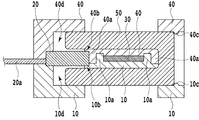
図1は、本発明に係る電流センサの実施形態1を説明するための斜視図で、図2は、図1のA−A線断面図である。本発明の実施形態1は、1次導体を樹脂ケースで完全に覆ったもので磁性体コアや磁気センサとの沿面距離の確保を行った例であり、磁性体コアのギャップが狭く磁気センサと磁性体コアとの距離確保が困難な場合に有効である。
Hereinafter, each embodiment of the present invention will be described with reference to the drawings.
[Embodiment 1]
FIG. 1 is a perspective view for explaining a first embodiment of a current sensor according to the present invention, and FIG. 2 is a cross-sectional view taken along line AA of FIG.
図中符号10は本体ケース部材(樹脂ケース)、10aは第1嵌合部、10bは磁気センサの取付溝、10cはコアの後端位置に設けられた係止部、10dは第1空隙部、20は磁気センサ、20aは磁気センサのリード線、30は被測定電流導体と接続される一次導体、40は蓋ケース部材(樹脂ケース)、40aは第2嵌合部、40bは磁気センサの位置決め溝、40cはコアの後端位置に設けられた係止部、40dは第2空隙部、50は磁性体コアを示している。
In the figure,
本発明の実施形態1の電流センサは、本体ケース部材10と磁気センサ20と一次導体30と蓋ケース部材40と磁性体コア50の5つの構成要素により簡便な組立可能に構成されている。この組立は、これらの構成要素を従来のような樹脂モールドや接着剤の使用を伴うことなく、嵌合又は接合のみによって実現されている。
The current sensor according to the first embodiment of the present invention is configured to be easily assembled by the five components of the main
本体ケース部材10は、上面に嵌め込み可能な沿面距離を有する第1嵌合部10aを備え、この第1嵌合部10aの長手方向で上面と下面との間に第1空隙部10dが形成され、第1嵌合部10aは凹凸部を有している。
The main
また、蓋ケース部材40は、下面に嵌め込み可能な沿面距離を有する第2嵌合部40aを備え、この第2嵌合部40aの長手方向で下面と上面との間に第2空隙部40dが形成され、第2嵌合部40aは凹凸部を有している。
The
これにより、本体ケース部材10の凹凸部と蓋ケース部材40の凹凸部とが互いに嵌め込まれるようになっている。なお、この凹凸部は、矩形又は波状の形状であることが望ましい。
Thereby, the uneven | corrugated | grooved part of the main
また、本体ケース部材10の磁気センサ20の搭載位置には取付溝10bが設けられ、同様に蓋ケース部材40の磁気センサ20の取付位置には取付溝40bが設けられ、これらの取付溝10b,40bにより磁気センサ20が、本体ケース部材10と蓋ケース部材40によって固定されるように構成されている。この磁気センサ20はホールICであることが望ましい。
Further, a mounting
また、磁気センサ20は、磁気検出素子と、この磁気検出素子からの検出信号を処理する信号処理回路とを備え、この信号処理回路には、磁気検出素子の検出特性のバラツキを低減するための不揮発性メモリ又は抵抗トリミングの調整可能な機能を有している。
In addition, the
1次導体30は、被測定電流導体に接続され、磁気センサ20の対面位置で直交方向に配置されるように、本体ケース部材10の2つの第1嵌合部10a間の凹部に嵌め込まれている。つまり、本体ケース部材10は、複数の第1嵌合部10a,10aを有し、1次導体30は、本体ケース部材10の第1嵌合部10a,10a間に組み込まれ、蓋ケース部材40によって押圧されるように構成されている。
The
断面コ字状の磁性体コア50は、1次導体30及び磁気センサ20を挟み込むように本体ケース部材10の第1空隙部10dと蓋ケース部材40の第2空隙部40dとに挿入固定されるように構成されている。また、この磁性体コア50の断面コ字状の形状は、断面U字状又は先端が狭められた断面C字状の形状を含んでいる。
The U-shaped
また、磁性体コア50の後端部、つまり、断面コ字状にともなうギャップ部の反対側の上下端部を止めるように、本体ケース部材10と蓋ケース部材40の磁性体コア50の後端位置には突起からなる係止部10c,40cが設けられている。
In addition, the rear end of the
このようにして、本体ケース部材10と蓋ケース部材40の第1及び第2嵌合部10a,40aで沿面距離を確保するとともに、磁性体コア50のギャップ部に配置された磁気センサ20により磁性体コア50に生じる磁束変化を電流として検出することが可能である。
In this manner, the creepage distance is ensured by the first and second
[実施形態2]
図3は、本発明に係る電流センサの実施形態2を説明するための斜視図で、図4は、図3のB−B線断面図である。本発明の実施形態2は、磁気センサを樹脂ケースで完全に覆ったもので、1次導体や磁性体コアから磁気センサの端子までの沿面距離を確保した例であり、実効電流の大きい大電流測定の場合、1次導体を厚くしなければならず、そのため磁性体コアと1次導体間の距離確保が難しい場合に有効である。
[Embodiment 2]
FIG. 3 is a perspective view for explaining a second embodiment of the current sensor according to the present invention, and FIG. 4 is a sectional view taken along line BB of FIG. Embodiment 2 of the present invention is an example in which the magnetic sensor is completely covered with a resin case, and a creeping distance from the primary conductor or magnetic core to the terminal of the magnetic sensor is ensured. In the case of measurement, the primary conductor must be thickened, which is effective when it is difficult to secure the distance between the magnetic core and the primary conductor.
上述した実施形態1との構成上の相違点は、実施形態2においては、磁気センサの全体が、本体ケース部材と蓋ケース部材とによって密接に挟持されている点の他に、本体ケース部材と蓋ケース部材との嵌合が1箇所のみであり、一次導体と磁性体コアとが空隙部を介して絶縁されている点である。 The difference in configuration from the first embodiment described above is that, in the second embodiment, in addition to the fact that the entire magnetic sensor is closely held between the main body case member and the lid case member, There is only one fitting with the lid case member, and the primary conductor and the magnetic core are insulated via the gap.
図中符号110は本体ケース部材(樹脂ケース)、110aは第1嵌合部、110bは磁気センサの取付溝、110cは磁性体コアの後端位置に設けられた係止部、110dは第1空隙部、120は磁気センサ、120aは磁気センサのリード線、130は被測定電流導体と接続される一次導体、140は蓋ケース部材(樹脂ケース)、140aは第2嵌合部、140bは磁気センサの位置決め溝、140cは磁性体コアの後端位置に設けられた係止部、140dは第2空隙部、150は磁性体コアを示している。
In the figure,
本発明の実施形態2の電流センサは、本体ケース部材110と磁気センサ120と一次導体130と蓋ケース部材140と磁性体コア150の5つの構成要素により簡便な組立可能に構成されている。この組立は、これらの構成要素を従来のような樹脂モールドや接着剤の使用を伴うことなく、嵌合又は接合のみによって実現されている。
The current sensor according to the second embodiment of the present invention is configured to be easily assembled by the five components of the main
本体ケース部材110は、上面に嵌め込み可能な沿面距離を有する第1嵌合部110aを備え、この第1嵌合部110aの長手方向で上面と下面との間に第1空隙部110dが形成され、第1嵌合部110aは凹凸部を有している。
The
また、蓋ケース部材140は、下面に嵌め込み可能な沿面距離を有する第2嵌合部140aを備え、この第2嵌合部140aの長手方向で下面と上面との間に第2空隙部140dが形成され、第2嵌合部140aは凹凸部を有している。
The
これにより、本体ケース部材110の凹凸部と蓋ケース部材140の凹凸部とが互いに嵌め込まれるようになっている。なお、この凹凸部は、矩形又は波状の形状でもよいことは、上述した実施形態1と同様である。
Thereby, the uneven part of the main
上述した実施形態1では、第1嵌合部10aと第2嵌合部40aとが複数組あったが、つまり、磁気センサ20と1次導体30との間に1組の嵌合部が設けられ、1次導体30と磁性体コアとの間にもう一組の嵌合部が設けられていたが、この実施形態2では磁気センサ120と1次導体130との間に1組の嵌合部が設けられているだけで、一次導体130と磁性体コア150との絶縁は空隙でなされている。
In the first embodiment described above, there are a plurality of sets of the first
また、本体ケース部材110の磁気センサ120の搭載位置には取付溝110bが設けられ、同様に蓋ケース部材140の磁気センサ120の取付位置には取付溝140bが設けられ、これらの取付溝110b,140bにより磁気センサ120が、本体ケース部材110と蓋ケース部材140によって密接に固定されるように構成されている。この磁気センサ120はホールICであることが望ましい。なお、磁気センサ120の構成については、上述した実施形態1の場合と同様である。
Further, the mounting
1次導体130は、被測定電流導体に接続され、磁気センサ120の対面位置で直交方向に配置されるように、第1嵌合部110aと第2嵌合部140aに接合配置されている。
The
断面コ字状の磁性体コア150は、1次導体130及び磁気センサ120を挟み込むように本体ケース部材110の第1空隙部110dと蓋ケース部材140の第2空隙部140dとに挿入固定されるように構成されている。この磁性体コアの形状については、上述した実施形態1の場合と同様である。また、磁性体コア150の後端部、つまり、断面コ字状にともなうギャップ部の反対側の上下端部を止めるように、本体ケース部材110と蓋ケース部材140の磁性体コア150の後端位置には突起の係止部110c,140cが設けられている。
The U-shaped
このようにして、本体ケース部材110と蓋ケース部材140の第1及び第2嵌合部110a,140aで沿面距離を確保するとともに、磁性体コア150のギャップ部に配置された磁気センサ120により磁性体コア150に生じる磁束変化を電流として検出することが可能である。
In this manner, the creepage distance is secured by the first and second
図5は、本発明の実施形態1又は2における磁性体コアと、蓋ケース部材及び本体ケース部材との係合手段の実施例1を説明するための断面図である。上述して本発明の実施形態1及び2における磁性体コアと、蓋ケース部材及び本体ケース部材との係合手段は、この実施例1の係合手段を用いている。
FIG. 5 is a cross-sectional view for explaining Example 1 of the engaging means of the magnetic core, the lid case member, and the main body case member in
磁性体コア50の後端部、つまり、断面コ字状のギャップ部201の反対側の上下端部を止めるように、本体ケース部材10と蓋ケース部材40の磁性体コア50の後端位置には突起からなる係止部10c,40cが設けられている。
At the rear end position of the
このような構成により、本体ケース部材10と蓋ケース部材40の磁性体コア50の後端部に少なくとも1箇所に突起を設けることで、磁性体コア50のケース部材内への挿入後に接着することなく磁性体コアを固定することができる。また、この突起を前述の上下端部以外の左右方向に設けても良い。この係止部は、フェライト製の磁性体コアなどの強度的に脆く、外力によりコアにひびや欠けが発生し易い材料の場合に都合が良い。なお、図3に示した本発明の実施形態2においても同様である。
With such a configuration, at least one protrusion is provided at the rear end portion of the
図6は、本発明の実施形態1又は2における磁性体コアと、蓋ケース部材及び本体ケース部材との係合手段の実施例2を説明するための断面図である。
FIG. 6 is a cross-sectional view for explaining Example 2 of the engaging means for the magnetic core, the lid case member, and the main body case member in
磁性体コア50の後端部に、断面コ字状のギャップ部201の反対側の上下端部を止めるように突起50aを設け、本体ケース部材10と蓋ケース部材40の磁性体コア50の後端位置には、磁性体コア50の突起50aを受け入れる切欠部40eが設けられている。
Protrusions 50 a are provided at the rear end of the
このような構成により、磁性体コアに加わるストレスが最後の一押しのみであるため、磁性体コアへのダメージが少なく、挿入作業が容易になる。この係止部は、微細加工が容易でかつ高い強度を有するケイ素鋼などの金属コアの場合に適している。なお、図3に示した本発明の実施形態2においても同様である。 With such a configuration, since the stress applied to the magnetic core is only the last push, the damage to the magnetic core is small and the insertion work is facilitated. This locking portion is suitable for a metal core such as silicon steel that is easy to finely process and has high strength. The same applies to Embodiment 2 of the present invention shown in FIG.
このように、上述した係止部の実施例1及び2において、接着工程を省くことで熱効果処置が不要になり、その結果、磁気センサへの熱ストレスを低減することができ、信頼性の向上が図れるとともに製造工程の短縮が図れる。 As described above, in the first and second embodiments of the locking portion described above, the thermal effect treatment becomes unnecessary by omitting the bonding step, and as a result, the thermal stress on the magnetic sensor can be reduced, and the reliability can be reduced. The improvement can be achieved and the manufacturing process can be shortened.
次に、本発明の電流センサの組立方法について以下に説明する。
図7(a)乃至(e)は、本発明に係る電流センサの組立方法を説明するための工程図で、図8は、本発明に係る電流センサの組立方法を説明するためのフローチャートを示す図である。なお、図2においては組み立て後の断面図が示されているが、この図7(a)乃至(e)においては、組立に必要な種々の構成要素を備えている。なお、以下の組立方法は、上述した実施形態1の場合について説明する。
Next, a method for assembling the current sensor of the present invention will be described below.
FIGS. 7A to 7E are process diagrams for explaining a current sensor assembling method according to the present invention, and FIG. 8 is a flowchart for explaining a current sensor assembling method according to the present invention. FIG. 2 shows a cross-sectional view after assembly. In FIGS. 7A to 7E, various components necessary for assembly are provided. In addition, the following assembly method demonstrates the case of
まず、上面に嵌め込み可能な沿面距離を有する第1嵌合部10aを備え、この第1嵌合部10aの長手方向で上面と下面との間に第1空隙部10dが形成されている本体ケース部材10を準備する(図8ステップS1)。
First, a main body case including a first
この本体ケース部材10は、磁性体コア50側の隅に上部右嵌合止め11と上部左嵌合止め12とを備え、磁気センサ20側の隅に下部左嵌合止め13と下部右嵌合止め14とを備えている。
The
また、本体ケース部材10の上面の一次導体30のカバー用溝16が設けられ、その溝16の表面に一次導体30の位置決め用ピン15が設けられており、この位置決め用ピン15と一次導体30に設けられた嵌着溝31とが嵌るようになっている。
Further, the
また、本体ケース部材10の上面において、溝16に隣接するようにして端部に蓋ケース部材40との位置合わせピン17が立設され、また、本体ケース部材10の上面において、この位置合わせピン17と磁気センサ20の取り付け側との間に磁気センサの位置決め溝18が設けられ、この磁気センサ20の取り付け側には磁気センサ20の複数のリード線20aに対応する複数の区分け溝19を設けて区分け部が形成されている。この区分け部によりケース内への塵の進入や、リード線間の短絡を防ぐことができる。
Further, on the upper surface of the main
次に、磁気センサ20の対面位置で直交方向に、被測定電流導体に接続される1次導体30を配置する(図7(a)及び図8ステップS2)。つまり、上述したように、本体ケース部材10に設けられた位置決め用ピン15と一次導体30に設けられた嵌着溝31とが嵌め合わされて嵌着される。
Next, the
次に、本体ケース部材10に設けられた位置決め溝18に磁気センサ20を搭載し(図7(b)及び図8ステップS3)、磁気センサ20のリード線20aは、区分け部を構成する複数の区分け溝19によって複数のリード線20aの各々は区分けされる。
Next, the
次に、磁気センサ20と1次導体30とを覆うように、下面に本体ケース部材10の第1嵌合部10aに嵌め込み可能な沿面距離を有する第2嵌合部40aを備え、この第2嵌合部40aの長手方向で下面と上面との間に第2空隙部40dが形成されている蓋ケース部材40を準備する(図8ステップS4)。
Next, a second
この蓋ケース部材40は、本体ケース部材10に設けられた、上部右嵌合止め11と上部左嵌合止め12と、下部左嵌合止め13と下部右嵌合止め14に対応するように、上部右嵌合爪41と上部左嵌合爪42と、下部左嵌合爪43と下部右嵌合爪44とを備えている。
The
また、蓋ケース部材40には、本体ケース部材10の上面に嵌着された一次導体30を覆うカバー用溝46が設けられ、また、本体ケース部材10の上面に設けられた位置合わせピン17に対応するように、位置合わせ溝47が設けられている。また、本体ケース部材10に設けられた磁気センサの位置決め溝18に対応した磁気センサの位置決め溝48が設けられている。
The
次に、蓋ケース部材40を本体ケース部材10に被せる(図7(c)及び図8ステップS5)。この場合、本体ケース部材10に設けられた上部右嵌合止め11が、蓋ケース部材40に設けられた上部右嵌合爪41と嵌合するように位置決めされ、上部左嵌合止め12が上部左嵌合爪42と、下部左嵌合止め13が下部左嵌合爪43と、下部右嵌合止め14が下部右嵌合爪44と、位置合わせピン17が位置合わせ溝47とそれぞれ嵌合するように位置決めされる。
Next, the
次に、1次導体30を挟み込むように本体ケース部材10と蓋ケース部材40の第1空隙部10dと第2空隙部40dに断面コ字状の磁性体コア50を挿入固定する(図7(d)及び図8ステップS6)。
Next, a U-shaped
なお、実施形態2における組立方法についても、上述した実施形態1の組立方法と同様に実施される。 The assembly method according to the second embodiment is also performed in the same manner as the assembly method according to the first embodiment described above.
10,110 本体ケース部材
10a,110a 第1嵌合部
10b,110b 磁気センサの取付溝
10c,110c コアの後端位置に設けられた係止部
10d,110d 第1空隙部
11 上部右嵌合止め
12 上部左嵌合止め
13 下部左嵌合止め
14 下部右嵌合止め
15 位置決め用ピン
16 本体ケース側のカバー用溝
17 位置合わせピン
18 本体ケース側の位置決め溝
19 区分け溝
20,120 磁気センサ
20a,120a 磁気センサのリード線
30,130 被測定電流導体と接続される一次導体
31 嵌着溝
40,140 蓋ケース部材
40a,140a 第2嵌合部
40b,140b 磁気センサの位置決め溝
40c,140c コアの後端位置に設けられた係止部
40d,140d 第2空隙部
40e,140e 切欠部
41 上部右嵌合爪
42 上部左嵌合爪
43 下部左嵌合爪
44 下部右嵌合爪
46 蓋ケース側のカバー用溝
47 本体ケース側の位置合わせ溝
48 蓋ケース側の位置決め溝
50,150 コア
50a,150a 突起
201 ギャップ部
10, 110 Main
Claims (15)
該本体ケース部材の前記上面側に搭載される磁気センサと、
被測定電流導体に接続され、前記磁気センサの対面位置で直交方向に配置される1次導体と、
前記磁気センサと前記1次導体とを覆うように、下面に前記本体ケース部材の前記第1嵌合部に嵌め込み可能な沿面距離を有する第2嵌合部を備え、該第2嵌合部の長手方向で前記下面と上面との間に第2空隙部が形成されている蓋ケース部材と、
前記1次導体を挟み込むように前記本体ケース部材と前記蓋ケース部材の前記第1及び第2空隙部に挿入固定される断面コ字状の磁性体コアとを備え、
前記本体ケース部材と前記蓋ケース部材の前記第1及び第2嵌合部で前記沿面距離を確保するとともに、前記磁性体コアの前記断面コ字状にともなうギャップ部に配置された前記磁気センサにより前記磁性体コアに生じる磁束変化を電流として検出することを特徴とする電流センサ。 A body case member comprising a first fitting portion having a creeping distance that can be fitted into the upper surface, wherein a first gap is formed between the upper surface and the lower surface in the longitudinal direction of the first fitting portion;
A magnetic sensor mounted on the upper surface side of the main body case member;
A primary conductor connected to the current conductor to be measured and arranged in an orthogonal direction at the facing position of the magnetic sensor;
A second fitting portion having a creeping distance that can be fitted into the first fitting portion of the main body case member on a lower surface so as to cover the magnetic sensor and the primary conductor; A lid case member in which a second gap is formed between the lower surface and the upper surface in the longitudinal direction;
A main body case member and a U-shaped magnetic core inserted into and fixed to the first and second gap portions of the lid case member so as to sandwich the primary conductor;
The magnetic sensor disposed in the gap portion of the magnetic core having the U-shaped cross section while securing the creepage distance at the first and second fitting portions of the main body case member and the lid case member. A current sensor that detects a change in magnetic flux generated in the magnetic core as a current.
前記磁気センサの対面位置で直交方向に、被測定電流導体に接続される1次導体を配置するステップと、
前記本体ケース部材の前記上面側に磁気センサを搭載するステップと、
前記磁気センサと前記1次導体とを覆うように、下面に前記本体ケース部材の前記第1嵌合部に嵌め込み可能な沿面距離を有する第2の嵌合部を備え、該第2嵌合部の長手方向で前記下面と上面との間に第2空隙部が形成されている蓋ケース部材を前記本体ケース部材に嵌め込むステップと、
前記1次導体を挟み込むように前記本体ケース部材と前記蓋ケース部材の前記第1及び第2空隙部に断面コ字状のコアを挿入固定するステップとを有し、
前記本体ケース部材と前記蓋ケース部材の前記第1及び第2嵌合部で前記沿面距離を確保するとともに、前記コアの前記断面コ字状にともなうギャップ部に配置された前記磁気センサにより前記コアに生じる磁束変化を電流として検出することを特徴とする電流センサの組立方法。 A body case member is provided that includes a first fitting portion having a creeping distance that can be fitted into the upper surface, and in which a first gap is formed between the upper surface and the lower surface in the longitudinal direction of the first fitting portion. Steps,
Disposing a primary conductor connected to a current conductor to be measured in an orthogonal direction at a facing position of the magnetic sensor;
Mounting a magnetic sensor on the upper surface side of the main body case member;
A second fitting portion having a creeping distance that can be fitted into the first fitting portion of the main body case member on the lower surface so as to cover the magnetic sensor and the primary conductor; Fitting a lid case member in which a second gap is formed between the lower surface and the upper surface in the longitudinal direction of the main body case member;
Inserting and fixing a U-shaped core in the first and second gaps of the body case member and the lid case member so as to sandwich the primary conductor,
The core is secured by the magnetic sensor disposed in the gap portion of the core with the first and second fitting portions of the main body case member and the lid case member, and at the gap portion with the U-shaped cross section of the core. A method for assembling a current sensor, wherein a change in magnetic flux generated in the current sensor is detected as a current.
Priority Applications (1)
| Application Number | Priority Date | Filing Date | Title |
|---|---|---|---|
| JP2009271585A JP5452190B2 (en) | 2009-11-30 | 2009-11-30 | Current sensor and assembly method thereof |
Applications Claiming Priority (1)
| Application Number | Priority Date | Filing Date | Title |
|---|---|---|---|
| JP2009271585A JP5452190B2 (en) | 2009-11-30 | 2009-11-30 | Current sensor and assembly method thereof |
Publications (2)
| Publication Number | Publication Date |
|---|---|
| JP2011112604A JP2011112604A (en) | 2011-06-09 |
| JP5452190B2 true JP5452190B2 (en) | 2014-03-26 |
Family
ID=44235036
Family Applications (1)
| Application Number | Title | Priority Date | Filing Date |
|---|---|---|---|
| JP2009271585A Active JP5452190B2 (en) | 2009-11-30 | 2009-11-30 | Current sensor and assembly method thereof |
Country Status (1)
| Country | Link |
|---|---|
| JP (1) | JP5452190B2 (en) |
Families Citing this family (3)
| Publication number | Priority date | Publication date | Assignee | Title |
|---|---|---|---|---|
| JP5948889B2 (en) * | 2012-01-20 | 2016-07-06 | 株式会社オートネットワーク技術研究所 | Current detector |
| JP2014035322A (en) * | 2012-08-10 | 2014-02-24 | Tokai Rika Co Ltd | Core holder and current sensor |
| JP2016099320A (en) * | 2014-11-26 | 2016-05-30 | アイシン精機株式会社 | Current sensor |
Family Cites Families (10)
| Publication number | Priority date | Publication date | Assignee | Title |
|---|---|---|---|---|
| JP2589275B2 (en) * | 1994-04-13 | 1997-03-12 | 東洋通信機株式会社 | Insulation cap for current detector |
| JPH1031038A (en) * | 1996-07-12 | 1998-02-03 | Togami Electric Mfg Co Ltd | Current sensor |
| JP2002243767A (en) * | 2001-02-21 | 2002-08-28 | Stanley Electric Co Ltd | Electric current detector |
| JP2002296305A (en) * | 2001-04-02 | 2002-10-09 | Jeco Co Ltd | Core for current sensor |
| JP3896590B2 (en) * | 2002-10-28 | 2007-03-22 | サンケン電気株式会社 | Current detector |
| EP1452878A1 (en) * | 2003-02-27 | 2004-09-01 | Liaisons Electroniques-Mecaniques Lem S.A. | Electric current sensor |
| US20070279053A1 (en) * | 2006-05-12 | 2007-12-06 | Taylor William P | Integrated current sensor |
| JP2008020404A (en) * | 2006-07-14 | 2008-01-31 | Asahi Kasei Electronics Co Ltd | Current detection mechanism and method of assembling the same |
| JP4424412B2 (en) * | 2007-11-21 | 2010-03-03 | 株式会社デンソー | Current sensor |
| EP2083277B1 (en) * | 2008-01-25 | 2011-01-05 | Liaisons Electroniques-Mecaniques Lem S.A. | Electrical current sensor |
-
2009
- 2009-11-30 JP JP2009271585A patent/JP5452190B2/en active Active
Also Published As
| Publication number | Publication date |
|---|---|
| JP2011112604A (en) | 2011-06-09 |
Similar Documents
| Publication | Publication Date | Title |
|---|---|---|
| JP5838210B2 (en) | Toroidal fluxgate current converter | |
| TWI445989B (en) | Electromagnetic coil structure having a flat conductive track, magnetic core and magneto electronic angle sensor | |
| CN107276258B (en) | Stator structure and rotary transformer | |
| WO2010110257A1 (en) | Bus bar device and fusible link unit | |
| US11187601B2 (en) | Sensor device | |
| JP2019009336A (en) | Noise reduction unit | |
| KR101795326B1 (en) | Connector with sensor | |
| CN108735459B (en) | Noise filter and noise reduction unit | |
| CN108808898B (en) | Stator and rotary transformer | |
| US10784037B2 (en) | Reactor having temperature sensor attached to terminal base unit | |
| JP5252207B2 (en) | Reactor and converter | |
| WO2012157362A1 (en) | Current detecting apparatus | |
| US20200280236A1 (en) | Stator, stator assembly, and transducer for converting between electrical energy and mechanical energy | |
| JP5452190B2 (en) | Current sensor and assembly method thereof | |
| CN109473255B (en) | Coil device | |
| JP5970164B2 (en) | Transformer module and DC-DC converter device | |
| JP2012237582A (en) | Current sensor | |
| JP6608864B2 (en) | Resolver | |
| WO2013153699A1 (en) | Electrical junction box and electrical current sensor | |
| KR200461696Y1 (en) | Current sensor | |
| US20160061865A1 (en) | Structure of mounting current sensor to battery cable | |
| JP6897329B2 (en) | Current sensor | |
| JP7418243B2 (en) | mold connector | |
| JP5228071B2 (en) | Molded transformer | |
| TWI411787B (en) | Current sensor |
Legal Events
| Date | Code | Title | Description |
|---|---|---|---|
| A621 | Written request for application examination |
Free format text: JAPANESE INTERMEDIATE CODE: A621 Effective date: 20121002 |
|
| RD02 | Notification of acceptance of power of attorney |
Free format text: JAPANESE INTERMEDIATE CODE: A7422 Effective date: 20121002 |
|
| RD04 | Notification of resignation of power of attorney |
Free format text: JAPANESE INTERMEDIATE CODE: A7424 Effective date: 20121002 |
|
| A977 | Report on retrieval |
Free format text: JAPANESE INTERMEDIATE CODE: A971007 Effective date: 20131212 |
|
| TRDD | Decision of grant or rejection written | ||
| A01 | Written decision to grant a patent or to grant a registration (utility model) |
Free format text: JAPANESE INTERMEDIATE CODE: A01 Effective date: 20131217 |
|
| A61 | First payment of annual fees (during grant procedure) |
Free format text: JAPANESE INTERMEDIATE CODE: A61 Effective date: 20131227 |
|
| R150 | Certificate of patent or registration of utility model |
Ref document number: 5452190 Country of ref document: JP Free format text: JAPANESE INTERMEDIATE CODE: R150 Free format text: JAPANESE INTERMEDIATE CODE: R150 |
|
| S531 | Written request for registration of change of domicile |
Free format text: JAPANESE INTERMEDIATE CODE: R313531 |
|
| R350 | Written notification of registration of transfer |
Free format text: JAPANESE INTERMEDIATE CODE: R350 |