JP5434719B2 - Optical filters and analytical instruments - Google Patents
Optical filters and analytical instruments Download PDFInfo
- Publication number
- JP5434719B2 JP5434719B2 JP2010063923A JP2010063923A JP5434719B2 JP 5434719 B2 JP5434719 B2 JP 5434719B2 JP 2010063923 A JP2010063923 A JP 2010063923A JP 2010063923 A JP2010063923 A JP 2010063923A JP 5434719 B2 JP5434719 B2 JP 5434719B2
- Authority
- JP
- Japan
- Prior art keywords
- substrate
- optical filter
- mirror
- surface portion
- electrode
- Prior art date
- Legal status (The legal status is an assumption and is not a legal conclusion. Google has not performed a legal analysis and makes no representation as to the accuracy of the status listed.)
- Active
Links
- 230000003287 optical effect Effects 0.000 title claims description 52
- 239000000758 substrate Substances 0.000 claims description 75
- 239000000463 material Substances 0.000 claims description 18
- 238000001039 wet etching Methods 0.000 claims description 10
- 239000011521 glass Substances 0.000 claims description 7
- 238000001312 dry etching Methods 0.000 claims description 6
- 238000004519 manufacturing process Methods 0.000 description 9
- KRHYYFGTRYWZRS-UHFFFAOYSA-N Fluorane Chemical compound F KRHYYFGTRYWZRS-UHFFFAOYSA-N 0.000 description 8
- 238000005530 etching Methods 0.000 description 7
- 238000000034 method Methods 0.000 description 7
- 238000006073 displacement reaction Methods 0.000 description 6
- 229910052751 metal Inorganic materials 0.000 description 6
- 239000002184 metal Substances 0.000 description 6
- 239000010936 titanium Substances 0.000 description 5
- VYPSYNLAJGMNEJ-UHFFFAOYSA-N Silicium dioxide Chemical compound O=[Si]=O VYPSYNLAJGMNEJ-UHFFFAOYSA-N 0.000 description 4
- 239000007864 aqueous solution Substances 0.000 description 4
- 229910052804 chromium Inorganic materials 0.000 description 4
- 238000000206 photolithography Methods 0.000 description 4
- 229910004298 SiO 2 Inorganic materials 0.000 description 3
- GWEVSGVZZGPLCZ-UHFFFAOYSA-N Titan oxide Chemical compound O=[Ti]=O GWEVSGVZZGPLCZ-UHFFFAOYSA-N 0.000 description 3
- 229910052782 aluminium Inorganic materials 0.000 description 3
- 239000004020 conductor Substances 0.000 description 3
- 229910052814 silicon oxide Inorganic materials 0.000 description 3
- 238000004544 sputter deposition Methods 0.000 description 3
- OGIDPMRJRNCKJF-UHFFFAOYSA-N titanium oxide Inorganic materials [Ti]=O OGIDPMRJRNCKJF-UHFFFAOYSA-N 0.000 description 3
- 238000002834 transmittance Methods 0.000 description 3
- XUIMIQQOPSSXEZ-UHFFFAOYSA-N Silicon Chemical compound [Si] XUIMIQQOPSSXEZ-UHFFFAOYSA-N 0.000 description 2
- 239000005388 borosilicate glass Substances 0.000 description 2
- 230000006378 damage Effects 0.000 description 2
- 229910052737 gold Inorganic materials 0.000 description 2
- 238000007733 ion plating Methods 0.000 description 2
- 230000035699 permeability Effects 0.000 description 2
- 229910021420 polycrystalline silicon Inorganic materials 0.000 description 2
- 229910052710 silicon Inorganic materials 0.000 description 2
- 239000010703 silicon Substances 0.000 description 2
- 229910052719 titanium Inorganic materials 0.000 description 2
- 238000007740 vapor deposition Methods 0.000 description 2
- 229910018072 Al 2 O 3 Inorganic materials 0.000 description 1
- 229910000838 Al alloy Inorganic materials 0.000 description 1
- OKTJSMMVPCPJKN-UHFFFAOYSA-N Carbon Chemical compound [C] OKTJSMMVPCPJKN-UHFFFAOYSA-N 0.000 description 1
- DGAQECJNVWCQMB-PUAWFVPOSA-M Ilexoside XXIX Chemical compound C[C@@H]1CC[C@@]2(CC[C@@]3(C(=CC[C@H]4[C@]3(CC[C@@H]5[C@@]4(CC[C@@H](C5(C)C)OS(=O)(=O)[O-])C)C)[C@@H]2[C@]1(C)O)C)C(=O)O[C@H]6[C@@H]([C@H]([C@@H]([C@H](O6)CO)O)O)O.[Na+] DGAQECJNVWCQMB-PUAWFVPOSA-M 0.000 description 1
- ZLMJMSJWJFRBEC-UHFFFAOYSA-N Potassium Chemical compound [K] ZLMJMSJWJFRBEC-UHFFFAOYSA-N 0.000 description 1
- 229910052581 Si3N4 Inorganic materials 0.000 description 1
- CDBYLPFSWZWCQE-UHFFFAOYSA-L Sodium Carbonate Chemical compound [Na+].[Na+].[O-]C([O-])=O CDBYLPFSWZWCQE-UHFFFAOYSA-L 0.000 description 1
- RTAQQCXQSZGOHL-UHFFFAOYSA-N Titanium Chemical compound [Ti] RTAQQCXQSZGOHL-UHFFFAOYSA-N 0.000 description 1
- 229910045601 alloy Inorganic materials 0.000 description 1
- 239000000956 alloy Substances 0.000 description 1
- 229910021417 amorphous silicon Inorganic materials 0.000 description 1
- 230000015572 biosynthetic process Effects 0.000 description 1
- 229910052799 carbon Inorganic materials 0.000 description 1
- 230000007547 defect Effects 0.000 description 1
- 238000000605 extraction Methods 0.000 description 1
- 230000002349 favourable effect Effects 0.000 description 1
- 239000010931 gold Substances 0.000 description 1
- CJNBYAVZURUTKZ-UHFFFAOYSA-N hafnium(iv) oxide Chemical compound O=[Hf]=O CJNBYAVZURUTKZ-UHFFFAOYSA-N 0.000 description 1
- 239000005355 lead glass Substances 0.000 description 1
- ORUIBWPALBXDOA-UHFFFAOYSA-L magnesium fluoride Chemical compound [F-].[F-].[Mg+2] ORUIBWPALBXDOA-UHFFFAOYSA-L 0.000 description 1
- 229910052759 nickel Inorganic materials 0.000 description 1
- PXHVJJICTQNCMI-UHFFFAOYSA-N nickel Substances [Ni] PXHVJJICTQNCMI-UHFFFAOYSA-N 0.000 description 1
- URLJKFSTXLNXLG-UHFFFAOYSA-N niobium(5+);oxygen(2-) Chemical compound [O-2].[O-2].[O-2].[O-2].[O-2].[Nb+5].[Nb+5] URLJKFSTXLNXLG-UHFFFAOYSA-N 0.000 description 1
- TWNQGVIAIRXVLR-UHFFFAOYSA-N oxo(oxoalumanyloxy)alumane Chemical compound O=[Al]O[Al]=O TWNQGVIAIRXVLR-UHFFFAOYSA-N 0.000 description 1
- BPUBBGLMJRNUCC-UHFFFAOYSA-N oxygen(2-);tantalum(5+) Chemical compound [O-2].[O-2].[O-2].[O-2].[O-2].[Ta+5].[Ta+5] BPUBBGLMJRNUCC-UHFFFAOYSA-N 0.000 description 1
- RVTZCBVAJQQJTK-UHFFFAOYSA-N oxygen(2-);zirconium(4+) Chemical compound [O-2].[O-2].[Zr+4] RVTZCBVAJQQJTK-UHFFFAOYSA-N 0.000 description 1
- 238000000059 patterning Methods 0.000 description 1
- 229920005591 polysilicon Polymers 0.000 description 1
- 229910052700 potassium Inorganic materials 0.000 description 1
- 239000011591 potassium Substances 0.000 description 1
- 239000011347 resin Substances 0.000 description 1
- 229920005989 resin Polymers 0.000 description 1
- 239000004065 semiconductor Substances 0.000 description 1
- HQVNEWCFYHHQES-UHFFFAOYSA-N silicon nitride Chemical compound N12[Si]34N5[Si]62N3[Si]51N64 HQVNEWCFYHHQES-UHFFFAOYSA-N 0.000 description 1
- 229910052709 silver Inorganic materials 0.000 description 1
- 239000004332 silver Substances 0.000 description 1
- 239000011734 sodium Substances 0.000 description 1
- 229910052708 sodium Inorganic materials 0.000 description 1
- ZCUFMDLYAMJYST-UHFFFAOYSA-N thorium dioxide Chemical compound O=[Th]=O ZCUFMDLYAMJYST-UHFFFAOYSA-N 0.000 description 1
- 229910003452 thorium oxide Inorganic materials 0.000 description 1
- 229910052725 zinc Inorganic materials 0.000 description 1
- 239000011701 zinc Substances 0.000 description 1
- 229910001928 zirconium oxide Inorganic materials 0.000 description 1
Images


Classifications
-
- G—PHYSICS
- G02—OPTICS
- G02B—OPTICAL ELEMENTS, SYSTEMS OR APPARATUS
- G02B5/00—Optical elements other than lenses
- G02B5/20—Filters
- G02B5/201—Filters in the form of arrays
-
- G—PHYSICS
- G02—OPTICS
- G02B—OPTICAL ELEMENTS, SYSTEMS OR APPARATUS
- G02B26/00—Optical devices or arrangements for the control of light using movable or deformable optical elements
- G02B26/001—Optical devices or arrangements for the control of light using movable or deformable optical elements based on interference in an adjustable optical cavity
-
- G—PHYSICS
- G02—OPTICS
- G02B—OPTICAL ELEMENTS, SYSTEMS OR APPARATUS
- G02B5/00—Optical elements other than lenses
- G02B5/20—Filters
- G02B5/28—Interference filters
- G02B5/284—Interference filters of etalon type comprising a resonant cavity other than a thin solid film, e.g. gas, air, solid plates
-
- G—PHYSICS
- G02—OPTICS
- G02F—OPTICAL DEVICES OR ARRANGEMENTS FOR THE CONTROL OF LIGHT BY MODIFICATION OF THE OPTICAL PROPERTIES OF THE MEDIA OF THE ELEMENTS INVOLVED THEREIN; NON-LINEAR OPTICS; FREQUENCY-CHANGING OF LIGHT; OPTICAL LOGIC ELEMENTS; OPTICAL ANALOGUE/DIGITAL CONVERTERS
- G02F1/00—Devices or arrangements for the control of the intensity, colour, phase, polarisation or direction of light arriving from an independent light source, e.g. switching, gating or modulating; Non-linear optics
- G02F1/01—Devices or arrangements for the control of the intensity, colour, phase, polarisation or direction of light arriving from an independent light source, e.g. switching, gating or modulating; Non-linear optics for the control of the intensity, phase, polarisation or colour
- G02F1/21—Devices or arrangements for the control of the intensity, colour, phase, polarisation or direction of light arriving from an independent light source, e.g. switching, gating or modulating; Non-linear optics for the control of the intensity, phase, polarisation or colour by interference
- G02F1/213—Fabry-Perot type
-
- G—PHYSICS
- G03—PHOTOGRAPHY; CINEMATOGRAPHY; ANALOGOUS TECHNIQUES USING WAVES OTHER THAN OPTICAL WAVES; ELECTROGRAPHY; HOLOGRAPHY
- G03F—PHOTOMECHANICAL PRODUCTION OF TEXTURED OR PATTERNED SURFACES, e.g. FOR PRINTING, FOR PROCESSING OF SEMICONDUCTOR DEVICES; MATERIALS THEREFOR; ORIGINALS THEREFOR; APPARATUS SPECIALLY ADAPTED THEREFOR
- G03F7/00—Photomechanical, e.g. photolithographic, production of textured or patterned surfaces, e.g. printing surfaces; Materials therefor, e.g. comprising photoresists; Apparatus specially adapted therefor
- G03F7/70—Microphotolithographic exposure; Apparatus therefor
- G03F7/70483—Information management; Active and passive control; Testing; Wafer monitoring, e.g. pattern monitoring
- G03F7/7055—Exposure light control in all parts of the microlithographic apparatus, e.g. pulse length control or light interruption
- G03F7/70575—Wavelength control, e.g. control of bandwidth, multiple wavelength, selection of wavelength or matching of optical components to wavelength
-
- H—ELECTRICITY
- H01—ELECTRIC ELEMENTS
- H01L—SEMICONDUCTOR DEVICES NOT COVERED BY CLASS H10
- H01L21/00—Processes or apparatus adapted for the manufacture or treatment of semiconductor or solid state devices or of parts thereof
- H01L21/02—Manufacture or treatment of semiconductor devices or of parts thereof
- H01L21/027—Making masks on semiconductor bodies for further photolithographic processing not provided for in group H01L21/18 or H01L21/34
- H01L21/0271—Making masks on semiconductor bodies for further photolithographic processing not provided for in group H01L21/18 or H01L21/34 comprising organic layers
- H01L21/0273—Making masks on semiconductor bodies for further photolithographic processing not provided for in group H01L21/18 or H01L21/34 comprising organic layers characterised by the treatment of photoresist layers
- H01L21/0274—Photolithographic processes
-
- G—PHYSICS
- G01—MEASURING; TESTING
- G01J—MEASUREMENT OF INTENSITY, VELOCITY, SPECTRAL CONTENT, POLARISATION, PHASE OR PULSE CHARACTERISTICS OF INFRARED, VISIBLE OR ULTRAVIOLET LIGHT; COLORIMETRY; RADIATION PYROMETRY
- G01J3/00—Spectrometry; Spectrophotometry; Monochromators; Measuring colours
- G01J3/12—Generating the spectrum; Monochromators
- G01J3/26—Generating the spectrum; Monochromators using multiple reflection, e.g. Fabry-Perot interferometer, variable interference filters
Description
本発明は、光フィルターおよび分析機器等に関する。 The present invention relates to an optical filter, an analytical instrument, and the like.
従来、入射光から目的とする波長の光を選択して出射する光フィルターとして、一対の基板を対向配置し、これら基板の対向する面それぞれにミラーを設け、これらのミラーの周囲にそれぞれ電極を設けるとともに、一方のミラーの周囲にダイアフラム部を設け、これら電極間の静電力によりダイアフラム部を変位させてこれらのミラー間のギャップ(エアーギャップ)を変化させることにより、所望の波長の光を取り出すエアーギャップ型かつ静電駆動型の光フィルターが知られている(例えば、特許文献1)。
このような光フィルターでは、製造時に一対のミラー間のギャップをサブミクロンから数ミクロンと非常に狭い範囲で制御する必要があり、しかも、これらのミラー間のギャップを精度良く維持し、かつ、所望のギャップ量に制御することが重要である。
Conventionally, as an optical filter that selects and emits light of a target wavelength from incident light, a pair of substrates are arranged to face each other, a mirror is provided on each of the opposing surfaces of these substrates, and an electrode is provided around each of these mirrors. In addition, a diaphragm portion is provided around one mirror, and the diaphragm portion is displaced by an electrostatic force between these electrodes to change a gap (air gap) between these mirrors, thereby extracting light of a desired wavelength. An air gap type and electrostatic drive type optical filter is known (for example, Patent Document 1).
In such an optical filter, it is necessary to control the gap between a pair of mirrors in a very narrow range from submicron to several microns at the time of manufacture, and furthermore, the gap between these mirrors can be accurately maintained and desired. It is important to control the gap amount.
ところでエアーギャップ型かつ静電駆動型の光フィルターでは、静電引力でダイアフラムを動かし、ミラー間のギャップを変化させる。このため、ダイアフラム部の厚みに応じて、ギャップの変位に必要な静電引力を生み出すための印加電圧が変化することになる。そのため、ダイアフラム部は印加電圧を低く抑えるためにも出来るだけ薄いことが望ましい。しかし、ダイアフラム部を薄くすることは強度低下に繋がり、繰り返しギャップ変位を行う光フィルターでは、変位を行う度にダイアフラム部に応力がかかるため、強度の低下は即ちダイアフラム部の破壊に繋がるという問題があった。
本発明は、上記の課題の少なくとも一部を解決するためになされたものであって、印加電圧を低く抑えるためにダイアフラム部を薄くした場合においても、ダイアフラム部の強度低下を抑制することができ、その結果、最大印加電圧が低くかつダイアフラム部の強度を高め、安定的なギャップ変位を可能とし、良好に駆動することができる光フィルター及びそれを備えた光モジュールを提供することを目的の一つとする。
By the way, in the air gap type and electrostatic drive type optical filter, the diaphragm is moved by electrostatic attraction to change the gap between the mirrors. For this reason, the applied voltage for producing the electrostatic attraction necessary for the displacement of the gap changes according to the thickness of the diaphragm portion. Therefore, it is desirable that the diaphragm portion be as thin as possible in order to keep the applied voltage low. However, thinning the diaphragm portion leads to a decrease in strength, and in an optical filter that repeatedly performs gap displacement, stress is applied to the diaphragm portion every time the displacement is performed, so that the decrease in strength leads to the destruction of the diaphragm portion. there were.
The present invention has been made to solve at least a part of the above problems, and even when the diaphragm portion is thinned in order to keep the applied voltage low, it is possible to suppress a decrease in strength of the diaphragm portion. As a result, it is an object of the present invention to provide an optical filter that has a low maximum applied voltage, increases the strength of the diaphragm portion, enables stable gap displacement, and can be driven satisfactorily, and an optical module including the same. I will.
本発明の光フィルターは、
下部基板と、
前記下部基板に設けられた下部ミラーと、
前記下部基板に設けられた下部電極と、
前記下部基板に対向して設けられた上部基板と、
前記上部基板に設けられ、前記下部ミラーと対向する上部ミラーと、
前記上部基板に設けられ、前記下部電極と対向する上部電極と、
を有し、
前記上部基板は、平面視において、前記上部ミラーを囲む溝を有し、
前記溝は、断面視において、第1側面部、第2側面部、底面部、前記第1側面部と前記底面部との間に位置する第1端部および前記第2側面部と前記底面部との間に位置する第2端部を有し、
前記第1端部および前記第2端部は曲面を有することを特徴とする。
本発明の光フィルターでは、溝の端部を曲面としている。これにより、ギャップ変位時に発生する溝の端部への応力集中が緩和され、ダイアフラム部の強度を向上させる。その結果、安定的なギャップ変位を可能とし、良好にギャップ駆動をすることができる。
The optical filter of the present invention is
A lower substrate,
A lower mirror provided on the lower substrate;
A lower electrode provided on the lower substrate;
An upper substrate provided facing the lower substrate ;
An upper mirror provided on the upper substrate and facing the lower mirror;
An upper electrode provided on the upper substrate and facing the lower electrode;
Have
The upper substrate has a groove surrounding the upper mirror in plan view,
The groove includes a first side surface portion, a second side surface portion, a bottom surface portion, a first end portion located between the first side surface portion and the bottom surface portion, and the second side surface portion and the bottom surface portion in a sectional view. A second end located between and
The first end and the second end have curved surfaces.
In the optical filter of the present invention, the end of the groove is a curved surface. As a result, the stress concentration at the end of the groove that occurs when the gap is displaced is alleviated, and the strength of the diaphragm is improved. As a result, stable gap displacement is possible, and good gap driving can be achieved.
上記に記載の光フィルターは、
前記底面部は平坦であり、
平面視において、前記上部電極は、前記底面部の下方の領域内の前記上部基板に設けられていることを特徴とする。
これにより、溝の歪みに伴う上部電極にクラック等が発生することを防止することができる。
The optical filter described above is
The bottom surface is flat;
In plan view, the upper electrode is provided on the upper substrate in a region below the bottom surface.
Thereby, it can prevent that a crack etc. generate | occur | produce in the upper electrode accompanying distortion of a groove | channel.
上記に記載の光フィルターは、
前記第1端部は、前記上部ミラー側に位置し、
前記第1端部は、平面視において、前記上部ミラーと重なっていないことを特徴とする。
これにより、上部ミラーに入射される光の進行が、ダイアフラム部の側面部によって、遮られることを抑制することができ、良好なセンシングが可能となる。
The optical filter described above is
The first end is located on the upper mirror side,
The first end portion does not overlap the upper mirror in plan view.
Accordingly, it is possible to suppress the progress of light incident on the upper mirror from being blocked by the side surface portion of the diaphragm portion, and good sensing can be performed.
上記に記載の光フィルターは、
前記下部基板および前記上部基板は、光透過性を有することを特徴とする。
このように、下部基板及び上部基板を、光透過性を有することとしたことにより、基板における光の透過率が向上し、取り出した光の強度も高くなる。よって、光の取り出し効率が向上する。
The optical filter described above is
The lower substrate and the upper substrate are light transmissive.
As described above, since the lower substrate and the upper substrate have optical transparency, the light transmittance in the substrate is improved, and the intensity of the extracted light is increased. Therefore, the light extraction efficiency is improved.
上記に記載の光フィルターは、
前記溝は、ドライエッチングを行った後に、ウェットエッチングを行うことにより形成されていることを特徴とする。
このように、加工にウェットエッチングを用いることで容易に端部の形状を曲面にすることが出来、端部への応力集中を緩和し、ダイアフラム部の強度を向上させることが出来る。またドライエッチングとウェットエッチングを組み合わせることで、溝の加工にかかる時間を短縮し、且つ、溝端部が曲面を有する構造とすることができ、端部への応力集中を緩和し、ダイアフラム部の強度を向上させることが出来る。その結果、安定的なギャップ変位を可能とし、良好に駆動することができる。
The optical filter described above is
The groove is formed by performing dry etching and then performing wet etching.
In this way, by using wet etching for processing, the shape of the end can be easily made a curved surface, the stress concentration on the end can be relaxed, and the strength of the diaphragm can be improved. Also, by combining dry etching and wet etching, the time required for groove processing can be shortened, and the groove end can have a curved surface structure, reducing stress concentration on the end and reducing the strength of the diaphragm. Can be improved. As a result, stable gap displacement is possible and good driving can be achieved.
本発明の分析機器は、上記に記載の光フィルターを用いることを特徴とする。 The analytical instrument of the present invention is characterized by using the optical filter described above.
以下、本発明にかかる実施形態の光フィルターについて説明する。ここでは、光フィルターとして、エアーギャップ型かつ静電駆動型の光フィルターについて説明する。 Hereinafter, an optical filter according to an embodiment of the present invention will be described. Here, an air gap type and electrostatic drive type optical filter will be described as the optical filter.
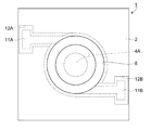
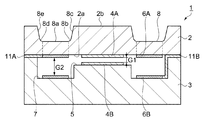
図1および図2において、符号1はエアーギャップ型で静電駆動型の光フィルターである。この光フィルター1は、上部基板2と、上部基板2に対向した状態で接合(または接着)された下部基板3と、上部基板2の下部基板3と対向する側の対向面2aの中央部に設けられた円形状のミラー4A(上部ミラー)と、下部基板3の上部基板2と対向する側の面の中央部に形成された第1の凹部5の底部中央にミラー4Aと第1のギャップG1を介して対向して設けられた円形状のミラー4B(下部ミラー)と、上部基板2のミラー4Aの周囲に設けられた円環状の電極6A(上部電極)と、下部基板3の第1の凹部5の周囲に形成された円環状の第2の凹部7に電極6Aと第2のギャップG2を介して対向して設けられた円環状の電極6B(下部電極)と、上部基板2の対向面2aの反対面側において、電極6Aとほぼ対応する位置にエッチング(選択除去)により形成された薄肉の円環状のダイアフラム部8とにより構成されている。
1 and 2,
ダイアフラム部8は第1側面部8c、第2側面部8e、底面部8a、第1側面部8cと底面部8aとの間に位置する第1端部8b、および第2側面部8eと底面部8aとの間に位置する第2端部8d、から構成される。また、ダイアフラム部8における、ミラー4A側に位置する第1端部8bは、平面視においてミラー4Aと重ならないように形成されている。このような構造とすることで、ミラー4Aに入射される光の進行が、ダイアフラム部8の第1側面部8cによって、遮られることを抑制することができる。
The
そして、第2のギャップG2を介して対向して設けられた電極6A、6Bと、ダイアフラム部8と、により、静電アクチュエーターが構成されている。
上部基板2および下部基板3の材料としてガラスを用いることができる。ガラスとしては、具体的には、ソーダガラス、結晶化ガラス、石英ガラス、鉛ガラス、カリウムガラス、ホウケイ酸ガラス、ホウケイ酸ナトリウムガラス、無アルカリガラス等が好適に用いられる。
And the electrostatic actuator is comprised by the
Glass can be used as the material of the
上部基板2及び下部基板3を共に光透過性を有する材料とすることにより、電磁波のうち所望の波長帯域の電磁波や可視光線を入射光として用いることができる。
また、上部基板2及び下部基板3を共に半導体材料、例えばシリコンで形成すれば、入射光として近赤外線を用いることができる。
By using both the
Further, if both the
ミラー4A、4Bは、第1のギャップG1を介して互いに対向して配置されたもので、高屈折率層と低屈折率層とが交互に複数積層された誘電体多層膜により構成されている。なお、ミラー4A、4Bは、誘電体多層膜に限定されることなく、例えば、銀を主成分とする合金膜や、それらの多層膜等を用いることもできる。
The
これらミラー4A、4Bのうち、一方のミラー4Aは変形可能な上部基板2に設けられているので可動ミラーと称し、他方のミラー4Bは変形しない下部基板3に設けられているので固定ミラーと称することもある。
Of these
この光フィルター1を可視光線の領域あるいは赤外線の領域で用いる場合、誘電体多層膜における高屈折率層を形成する材料としては、例えば、酸化チタン(Ti2O)、酸化タンタル(Ta2O5)、酸化ニオブ(Nb2O5)等が用いられる。また、光フィルター1を紫外線の領域で用いる場合、高屈折率層を形成する材料としては、例えば酸化アルミニウム(Al2O3)、酸化ハフニウム(HfO2)、酸化ジルコニウム(ZrO2)、酸化トリウム(ThO2)等が用いられる。
When the
一方、誘電体多層膜における低屈折率層を形成する材料としては、例えば、フッ化マグネシウム(MgF2)、酸化ケイ素(SiO2)等が用いられる。
この高屈折率層及び低屈折率層の層数及び厚みについては、必要とする光学特性に基づいて適宜に設定される。一般に、誘電体多層膜により反射膜(ミラー)を形成する場合、その光学特性を得るために必要な層数は12層以上である。
On the other hand, as a material for forming the low refractive index layer in the dielectric multilayer film, for example, magnesium fluoride (MgF 2 ), silicon oxide (SiO 2 ), or the like is used.
The number and thickness of the high refractive index layer and the low refractive index layer are appropriately set based on the required optical characteristics. In general, when a reflective film (mirror) is formed of a dielectric multilayer film, the number of layers necessary for obtaining the optical characteristics is 12 or more.
電極6A、6Bは、第2のギャップG2を介して互いに対向して配置されたもので、入力される駆動電圧に応じてこれら電極6A、6B間に静電力を発生させ、ミラー4A、4Bを互いに対向した状態で相対移動させる静電アクチュエーターの一部を構成するものである。
The
これにより、電極6A、6Bは、ダイアフラム部8を図2中上下方向に変位させてミラー4A、4B間の第1のギャップG1を変化させ、この第1のギャップG1に対応する波長の光を出射するようになっている。
As a result, the
また、電極6Aは、図2に示すように、平坦な面である底面部8aの下方の領域内に設けられている。仮に、電極6Aを、曲面を有する第1端部8b、第2端部8dと重なるように形成した場合、ダイアフラム部8の駆動によってダイアフラム部8が歪み、第1端部8b、第2端部8dの下方に位置する電極6Aに大きな応力が発生してしまう。それにより、電極6Aにクラック等の不具合が生じてしまう恐れがある。しかしながら、平坦な面である底面部8aの下方の領域内に電極6Aを形成することで、ダイアフラム部8の歪みに伴う電極6Aのクラック等を防止することができる。
As shown in FIG. 2, the
なお、本実施形態では、上部基板2の対向面2aと下部基板3に形成された第2の凹部7とは平行になっているので、電極6A、6B間も平行となっている。
これら電極6A、6Bを形成する材料としては導電性であればよく、特に限定はされないが、例えば、Cr、Al、Al合金、Ni、Zn、Ti、Au等の金属、あるいはカーボン、チタン等を分散した樹脂、多結晶シリコン(ポリシリコン)、アモルファスシリコン等のシリコン、窒化シリコン、ITO等の透明導電材料等が用いられる。
これら電極6A、6Bには、図1に示すように、配線11A、11Bが接続されており、これら電極6A、6Bは、これら配線11A、11Bを介して電源(図示せず)に接続されている。
In the present embodiment, since the facing
The material for forming these
As shown in FIG. 1,
なお、これら配線11A、11Bは、上部基板2に形成された配線溝12A、あるいは下部基板3に形成された配線溝12Bに形成されている。したがって、上部基板2と下部基板3との接合に干渉しないようになっている。
The
電源は、駆動信号として、電極6A、6Bに電圧を印加することにより、電極6A、6Bを駆動させ、これらの間に所望の静電力を発生させるものである。なお、この電源には制御装置(図示せず)が接続されており、この制御装置によって電源を制御することにより、電極6A、6B間の電位差を調整することができるようになっている。
The power source applies a voltage to the
ダイアフラム部8は、このダイアフラム部8が形成されていない上部基板2の箇所に比べて厚さが薄くなっている。このように、上部基板2のうち他の箇所に比べて厚さが薄い箇所は、弾性(可撓性)を有して変形可能(変位可能)になっており、これにより、このダイアフラム部8は、第1のギャップG1を変化させてミラー4A、4B間の間隔を所望の波長の光に対応する間隔に変化させることにより、所望の波長の光を出射させる波長選択機能を有するようになっている。
The
これらダイアフラム部8の形状や厚みは、所望の波長の範囲の光を出射させることができればよく、具体的には、ミラー4A、4B間の間隔の変化量及び変化の速さ等を勘案し、この光フィルター1に求められる出射光の波長の範囲に対応して設定される。
The shape and thickness of these
本実施形態の光フィルター1では、制御装置及び電源が駆動されず、したがって、電極6Aと電極6Bとの間に電圧が印加されていない場合、ミラー4Aとミラー4Bとは第1のギャップG1を介して対向している。そこで、この光フィルター1に光が入射すると、図3に示すように、この第1のギャップG1に対応した波長の光、例えば720nmの波長の光が出射されることとなる。
In the
ここで、制御装置及び電源を駆動させて電極6Aと電極6Bとの間に電圧を印加すると、これら電極6Aと電極6Bとの間には、電圧(電位差)の大きさに対応した静電力が発生する。このように、制御装置が電源を制御することにより、電極6A、6B間に所望の電圧を印加し、電極6Aと電極6Bとの間に所望の静電力を発生させることができる。このようにして電極6A、6B間に所望の静電力が発生すると、この静電力により電極6A、6Bが相互に引きつけられて上部基板2が下部基板3側に向かって変形し、ミラー4Aとミラー4Bとの第1のギャップG1が、電圧が印加されていない場合と比べて狭くなる。
この場合、静電力によりダイアフラム部8が稼動することで、第1端部8b、第2端部8dに応力が発生するが、本実施形態によれば第1端部8b、第2端部8dは丸み半径が大きな形状となるため、応力集中はし難くなり、繰り返しのダイアフラム部8の駆動に対しても破壊等が起き難く、良好な駆動が繰り返される。
Here, when a voltage is applied between the
In this case, when the
そこで、この光フィルター1に光が入射すると、図4に示すように、変位した第1のギャップG1に対応した波長の光、例えば590nmの波長の光が出射されることとなり、透過波長が短波長側にシフトすることとなる。
Therefore, when light enters the
次に、本実施形態の光フィルター1の製造方法について、図面を参照して説明する。図5〜9は、本実施形態の光フィルター1の製造方法を示す断面図である。
この製造方法は、[1]上部基板の加工工程、[2]下部基板の加工工程、を有している。以下、各工程について順次説明する。
Next, the manufacturing method of the
This manufacturing method includes [1] an upper substrate processing step and [2] a lower substrate processing step. Hereinafter, each process will be described sequentially.
[1]上部基板の加工工程
図5(a)に示すように、上部基板2の全面にマスク層51を成膜する。マスク層51を構成する材料としては、例えば、Cr/Au等の金属膜等を用いることができる。マスク層51の厚さは、特に限定されないが、0.01〜1μm程度とすることが好ましく、0.1〜0.3μm程度とすることがより好ましい。マスク層51が薄すぎると、上部基板2を十分に保護できない場合があり、マスク層51が厚すぎると、マスク層51の内部応力によりマスク層51が剥がれ易くなる場合がある。本実施形態では、マスク層51は、Cr/Au膜をスパッタ法によって成膜し、Cr、Auそれぞれの膜厚は0.01μm、0.3μmとしている。
[1] Upper Substrate Processing Step As shown in FIG. 5A, a
次に、図5(b)に示すように、マスク層51に、ダイアフラム部8を形成するための開口部51aを形成する。開口部51aは、例えばフォトリソグラフィー法により形成することができる。具体的には、マスク層51上に、開口部51aに対応したパターンを有するレジスト層(図示せず)を形成し、このレジスト層をマスクとして、マスク層51の一部を除去した後に、レジスト層を除去することで開口部51aが形成される。なお、マスク層51の一部除去は、ウェットエッチング等により行われる。
Next, as shown in FIG. 5B, an opening 51 a for forming the
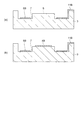
次に、図5(c)に示すように、ウェットエッチングによって上部基板2を食刻し、ダイアフラム部8を形成する。エッチング液としては、例えば、フッ酸水溶液や緩衝フッ酸水溶液(BHF)が等を用いることができる。また、これに変えて、ドライエッチングを行った後にウェットエッチングを行って、ダイアフラム部8を形成しても良い。これによると、溝の加工にかかる時間を短縮し、且つ、溝の第1端部8b、第2端部8dが曲面を有する構造とすることができ、端部への応力集中を緩和し、ダイアフラム部8の強度を向上させることが出来る。
Next, as shown in FIG. 5C, the
次に、図6(a)に示すように、電極6A、配線11Aを形成する。電極6A、配線11Aを構成する材料としては、例えばCr、Al等の金属膜やITOのような透明導電材料等を用いることができる。電極6A、配線11Aの厚さは、例えば、0.1〜0.2μmとするのが好ましい。
Next, as shown in FIG. 6A, an
これら電極6A、配線11Aを形成するためには、蒸着法、スパッタ法、イオンプレーティング法等によって金属膜等を成膜した後、フォトリソグラフィー法及びエッチングによってパターニングを行う。
In order to form these
次に、対向面2aのダイアフラム部8に囲まれた位置2a’にミラー4Aを形成する。例えば、高屈折率層を形成する材料として酸化チタン(Ti2O)、低屈折率層を形成する材料として酸化ケイ素(SiO2)を積層し、それらをリフトオフ法によりパターニングするとミラー4Aが得られる。
Next, the
[2]下部基板の加工工程
図7(a)に示すように、下部基板3の上部基板2との対向面3aにマスク層61を成膜する。マスク層61を構成する材料としては、一般的な材料レジスト材料を用いる。
次に、図7(b)に示すように、マスク層61に、第2の凹部7を形成するための開口部61aを形成する。開口部61aは、フォトリソグラフィー法により形成することができる。
[2] Lower Substrate Processing Step As shown in FIG. 7A, a
Next, as shown in FIG. 7B, an opening 61 a for forming the
次に、図7(c)に示すように、ウェットエッチングによって下部基板3を食刻し、第2の凹部7を形成する。エッチング液としては、例えば、フッ酸水溶液や緩衝フッ酸水溶液(BHF)等を用いることができる。なお、第2の凹部7の形成方法としては、ウェットエッチングに限られず、ドライエッチング等他のエッチング法を用いてもよい。
Next, as shown in FIG. 7C, the
次に、エッチングによってマスク層61を除去した後、第2の凹部7の形成と同じ要領で、第1の凹部5を形成する。具体的には、下部基板3上にマスク層62を成膜し、図8(a)に示すように、第1の凹部5を形成するための開口部62aを形成する。次いで、図8(b)に示すように、ウェットエッチングによって下部基板3を食刻して、第1の凹部5を形成する。その後、図8(c)に示すように、マスク層62をエッチングによって除去することによって、第1の凹部5及び第2の凹部7を備えた下部基板3が得られる。
Next, after removing the
次に、図9(a)に示すように、電極6B、配線11Bを形成する。電極6B、配線11Bを構成する材料としては、例えばCr、Al等の金属膜やITOのような透明導電材料等を用いることができる。電極6B、配線11Bの厚さは、例えば、0.1〜0.2μmとするのが好ましい。
これら電極6B、配線11Bを形成する、蒸着法、スパッタ法、イオンプレーティング法等によって金属膜等を成膜した後、フォトリソグラフィー法及びエッチングによってパターニングを行う。
Next, as shown in FIG. 9A, the
A metal film or the like is formed by vapor deposition, sputtering, ion plating or the like to form these
次に、上部基板2のミラー4Aに対向する位置にミラー4Bを形成する。例えば、高屈折率層を形成する材料として酸化チタン(Ti2O)、低屈折率層を形成する材料として酸化ケイ素(SiO2)を積層し、それらをリフトオフ法によりパターニングするとミラー4Bが得られる。
Next, the
以上説明したように、本実施形態の光フィルターによれば、選択的に波長を取り出すために第1のギャップG1を変動させる際にダイアフラム部8が稼動することで、第1端部8b、第2端部8dに応力が発生するが、本実施形態によれば第1端部8b、第2端部8dは丸み半径が大きな形状となるため、応力集中はし難くなり、繰り返しのダイアフラム部8の駆動に対しても破壊等が起き難く、良好な駆動が繰り返される。
As described above, according to the optical filter of the present embodiment, when the first gap G1 is changed to selectively extract the wavelength, the
なお、本発明の光フィルターは、色を測定する測色器やガスを測定するガス検出器等の分析機器に適用することができる。 The optical filter of the present invention can be applied to analytical instruments such as a colorimeter for measuring color and a gas detector for measuring gas.
1…光フィルター、2…上部基板、3…下部基板、4A,4B…ミラー、5…第1の凹部、6A,6B…電極、7…第2の凹部、8…ダイアフラム部、11A,11B…配線、G1…第1のギャップ、G2…第2のギャップ。
DESCRIPTION OF
Claims (5)
前記第1基板に設けられた第1ミラーと、
前記第1基板に設けられた第1電極と、
前記第1基板に対向して設けられた第2基板と、
前記第2基板に設けられ、前記第1ミラーと対向する第2ミラーと、
前記第2基板に設けられ、前記第1電極と対向する第2電極と、
を有し、
前記第2基板は、ガラス材料からなり、前記第1基板及び前記第2基板を厚さ方向から見た平面視において、前記第2ミラーを変位可能にする前記第2ミラーを囲む溝を有し、
前記溝は、前記第2基板の厚さ方向に沿った断面視において、第1側面部、第2側面部、底面部、前記第1側面部と前記底面部との間に位置する第1端部、および前記第2側面部と前記底面部との間に位置する第2端部を有し、
前記第1端部および前記第2端部は、ウェットエッチングにより前記溝の内部を曲率中心とする曲面を有し、
前記第1側面部および前記第2側面部は、前記底面部から離れるにしたがって前記溝の開口が広がるように傾斜し、前記第2側面部より前記第2ミラー側に位置する前記第1側面部が、前記平面視において、前記第2ミラーと離れていることを特徴とする光フィルター。 A first substrate;
A first mirror provided on the first substrate;
A first electrode provided on the first substrate;
A second substrate provided facing the first substrate;
A second mirror provided on the second substrate and facing the first mirror;
A second electrode provided on the second substrate and facing the first electrode;
Have
The second substrate is made of a glass material, and has a groove surrounding the second mirror that enables the second mirror to be displaced in a plan view of the first substrate and the second substrate viewed from the thickness direction. ,
The groove has a first side surface portion, a second side surface portion, a bottom surface portion, and a first end located between the first side surface portion and the bottom surface portion in a cross-sectional view along the thickness direction of the second substrate. And a second end portion located between the second side surface portion and the bottom surface portion,
It said first end and said second end, have a curved surface with the center of curvature inside of the trench by wet etching,
The first side surface portion and the second side surface portion are inclined so that the opening of the groove is widened as the distance from the bottom surface portion increases, and the first side surface portion is located closer to the second mirror than the second side surface portion. However, the optical filter is separated from the second mirror in the plan view .
前記底面部は平坦であり、
前記平面視において、前記第2電極は、前記第2基板の前記底面部と重なる領域に設けられていることを特徴とする光フィルター。 The optical filter according to claim 1,
The bottom surface is flat;
In the planar view, the second electrode is provided in a region overlapping the bottom surface of the second substrate.
前記第1基板および前記第2基板は、光透過性を有することを特徴とする光フィルター。 The optical filter according to any one of claims 1 to 2 ,
The optical filter, wherein the first substrate and the second substrate are light transmissive.
前記溝は、ドライエッチングを行った後に、前記ウェットエッチングを行うことにより形成されていることを特徴とする光フィルター。 The optical filter according to any one of claims 1 to 3 ,
The optical filter, wherein the groove is formed by performing the wet etching after performing the dry etching.
Priority Applications (12)
| Application Number | Priority Date | Filing Date | Title |
|---|---|---|---|
| JP2010063923A JP5434719B2 (en) | 2010-03-19 | 2010-03-19 | Optical filters and analytical instruments |
| US13/038,587 US20110228396A1 (en) | 2010-03-19 | 2011-03-02 | Optical filter and analytical instrument |
| KR1020110022649A KR20110105713A (en) | 2010-03-19 | 2011-03-15 | Optical filter and analytical instrument |
| TW100108982A TWI528050B (en) | 2010-03-19 | 2011-03-16 | Optical filter and analytical instrument |
| CN201110069658.4A CN102193187B (en) | 2010-03-19 | 2011-03-17 | Optical filter and analytical equipment thereof |
| EP13157164.8A EP2600194B1 (en) | 2010-03-19 | 2011-03-17 | Optical filter and analytical instrument |
| EP11158638.4A EP2367057B1 (en) | 2010-03-19 | 2011-03-17 | Optical filter and analytical instrument |
| EP13157161.4A EP2600192B1 (en) | 2010-03-19 | 2011-03-17 | Optical filter and analytical instrument |
| EP15185426.2A EP2985657B1 (en) | 2010-03-19 | 2011-03-17 | Optical filter and analytical instrument |
| EP13157159.8A EP2600191A3 (en) | 2010-03-19 | 2011-03-17 | Optical filter and analytical instrument |
| EP13157163.0A EP2600193A3 (en) | 2010-03-19 | 2011-03-17 | Optical filter and analytical instrument |
| US15/084,637 US9703092B2 (en) | 2010-03-19 | 2016-03-30 | Optical filter including a substrate having a groove with a pair of curved surfaces and analytical instrument |
Applications Claiming Priority (1)
| Application Number | Priority Date | Filing Date | Title |
|---|---|---|---|
| JP2010063923A JP5434719B2 (en) | 2010-03-19 | 2010-03-19 | Optical filters and analytical instruments |
Publications (3)
| Publication Number | Publication Date |
|---|---|
| JP2011197386A JP2011197386A (en) | 2011-10-06 |
| JP2011197386A5 JP2011197386A5 (en) | 2012-11-29 |
| JP5434719B2 true JP5434719B2 (en) | 2014-03-05 |
Family
ID=44260891
Family Applications (1)
| Application Number | Title | Priority Date | Filing Date |
|---|---|---|---|
| JP2010063923A Active JP5434719B2 (en) | 2010-03-19 | 2010-03-19 | Optical filters and analytical instruments |
Country Status (5)
| Country | Link |
|---|---|
| US (2) | US20110228396A1 (en) |
| EP (6) | EP2600194B1 (en) |
| JP (1) | JP5434719B2 (en) |
| KR (1) | KR20110105713A (en) |
| TW (1) | TWI528050B (en) |
Families Citing this family (8)
| Publication number | Priority date | Publication date | Assignee | Title |
|---|---|---|---|---|
| JP5434719B2 (en) | 2010-03-19 | 2014-03-05 | セイコーエプソン株式会社 | Optical filters and analytical instruments |
| JP5928992B2 (en) | 2010-10-07 | 2016-06-01 | セイコーエプソン株式会社 | Method for manufacturing tunable interference filter |
| JP6024086B2 (en) * | 2011-09-29 | 2016-11-09 | セイコーエプソン株式会社 | Wavelength variable interference filter, optical filter device, optical module, electronic device, and method of manufacturing wavelength variable interference filter |
| JP5910099B2 (en) | 2012-01-18 | 2016-04-27 | セイコーエプソン株式会社 | Interference filters, optical modules and electronics |
| JP6089674B2 (en) * | 2012-12-19 | 2017-03-08 | セイコーエプソン株式会社 | Wavelength variable interference filter, method for manufacturing wavelength variable interference filter, optical filter device, optical module, and electronic apparatus |
| US20140226988A1 (en) * | 2013-02-12 | 2014-08-14 | Avago Technologies General Ip (Singapore) Pte. Ltd | Bidirectional optical data communications module having reflective lens |
| WO2018037725A1 (en) * | 2016-08-24 | 2018-03-01 | 浜松ホトニクス株式会社 | Fabry-perot interference filter |
| JP7200842B2 (en) | 2019-06-21 | 2023-01-10 | セイコーエプソン株式会社 | Tunable Interference Filter |
Family Cites Families (29)
| Publication number | Priority date | Publication date | Assignee | Title |
|---|---|---|---|---|
| US4944187A (en) * | 1988-12-23 | 1990-07-31 | Rosemount Inc. | Multimodulus pressure sensor |
| JP2896725B2 (en) * | 1991-12-26 | 1999-05-31 | 株式会社山武 | Capacitive pressure sensor |
| JPH0675248A (en) * | 1992-06-30 | 1994-03-18 | Sony Corp | Active matrix substrate |
| JPH07113708A (en) * | 1993-10-20 | 1995-05-02 | Hitachi Ltd | Manufacture of semiconductor absolute pressure sensor |
| JP3178223B2 (en) * | 1994-03-10 | 2001-06-18 | 富士電機株式会社 | Manufacturing method of diaphragm |
| JPH09274860A (en) * | 1996-04-05 | 1997-10-21 | Dainippon Printing Co Ltd | Plasma display panel |
| JP2000124117A (en) * | 1998-10-14 | 2000-04-28 | Nikon Corp | Membrane mask and manufacture thereof |
| JP2002299229A (en) * | 2001-04-03 | 2002-10-11 | Nikon Corp | Electron beam exposing reticle blank manufacturing method and mask |
| JP2003057438A (en) | 2001-08-09 | 2003-02-26 | Yokogawa Electric Corp | Fabry-perot filter |
| JP2003185941A (en) * | 2001-12-20 | 2003-07-03 | Yokogawa Electric Corp | Fabry-perot filter |
| JP2004281256A (en) * | 2003-03-17 | 2004-10-07 | Nippon Sheet Glass Co Ltd | Display panel |
| JP2006085096A (en) * | 2004-09-17 | 2006-03-30 | Fujitsu Ltd | Exposure mask and its manufacturing method |
| JP2006208791A (en) * | 2005-01-28 | 2006-08-10 | Seiko Epson Corp | Tunable optical filter and method of manufacturing tunable optical filter |
| US20060274323A1 (en) * | 2005-03-16 | 2006-12-07 | Gibler William N | High intensity fabry-perot sensor |
| JP4548288B2 (en) * | 2005-09-22 | 2010-09-22 | セイコーエプソン株式会社 | Tunable filter |
| JP4547429B2 (en) | 2006-02-10 | 2010-09-22 | 東京エレクトロン株式会社 | Membrane structure and manufacturing method thereof |
| US7734131B2 (en) * | 2006-04-18 | 2010-06-08 | Xerox Corporation | Fabry-Perot tunable filter using a bonded pair of transparent substrates |
| US7835061B2 (en) * | 2006-06-28 | 2010-11-16 | Qualcomm Mems Technologies, Inc. | Support structures for free-standing electromechanical devices |
| JP5124121B2 (en) * | 2006-10-02 | 2013-01-23 | 株式会社アルバック | Etching method of glass substrate |
| JP2008130937A (en) * | 2006-11-22 | 2008-06-05 | Matsushita Electric Works Ltd | Method for manufacturing structure provided with diaphragm, and semiconductor device |
| US7715085B2 (en) * | 2007-05-09 | 2010-05-11 | Qualcomm Mems Technologies, Inc. | Electromechanical system having a dielectric movable membrane and a mirror |
| US7542200B1 (en) * | 2007-12-21 | 2009-06-02 | Palo Alto Research Center Incorporated | Agile beam steering mirror for active raster scan error correction |
| JP5446110B2 (en) * | 2008-03-31 | 2014-03-19 | セイコーエプソン株式会社 | Receiver |
| JP5564759B2 (en) * | 2008-04-02 | 2014-08-06 | セイコーエプソン株式会社 | Optical filter device |
| JP5369515B2 (en) * | 2008-06-26 | 2013-12-18 | セイコーエプソン株式会社 | Optical filter, method for manufacturing the same, and optical filter device module |
| JP5589459B2 (en) * | 2010-03-15 | 2014-09-17 | セイコーエプソン株式会社 | Optical filter, optical filter module, analytical instrument and optical instrument |
| JP5434719B2 (en) * | 2010-03-19 | 2014-03-05 | セイコーエプソン株式会社 | Optical filters and analytical instruments |
| JP5928992B2 (en) * | 2010-10-07 | 2016-06-01 | セイコーエプソン株式会社 | Method for manufacturing tunable interference filter |
| JP6089674B2 (en) * | 2012-12-19 | 2017-03-08 | セイコーエプソン株式会社 | Wavelength variable interference filter, method for manufacturing wavelength variable interference filter, optical filter device, optical module, and electronic apparatus |
-
2010
- 2010-03-19 JP JP2010063923A patent/JP5434719B2/en active Active
-
2011
- 2011-03-02 US US13/038,587 patent/US20110228396A1/en not_active Abandoned
- 2011-03-15 KR KR1020110022649A patent/KR20110105713A/en not_active Application Discontinuation
- 2011-03-16 TW TW100108982A patent/TWI528050B/en active
- 2011-03-17 EP EP13157164.8A patent/EP2600194B1/en active Active
- 2011-03-17 EP EP13157159.8A patent/EP2600191A3/en not_active Withdrawn
- 2011-03-17 EP EP15185426.2A patent/EP2985657B1/en active Active
- 2011-03-17 EP EP13157161.4A patent/EP2600192B1/en active Active
- 2011-03-17 EP EP11158638.4A patent/EP2367057B1/en active Active
- 2011-03-17 EP EP13157163.0A patent/EP2600193A3/en not_active Withdrawn
-
2016
- 2016-03-30 US US15/084,637 patent/US9703092B2/en active Active
Also Published As
| Publication number | Publication date |
|---|---|
| EP2600194B1 (en) | 2015-09-16 |
| EP2600194A3 (en) | 2013-12-25 |
| TWI528050B (en) | 2016-04-01 |
| EP2367057A3 (en) | 2012-01-11 |
| US20160209638A1 (en) | 2016-07-21 |
| EP2600192A2 (en) | 2013-06-05 |
| EP2985657A1 (en) | 2016-02-17 |
| US20110228396A1 (en) | 2011-09-22 |
| KR20110105713A (en) | 2011-09-27 |
| CN102193187A (en) | 2011-09-21 |
| TW201202744A (en) | 2012-01-16 |
| EP2985657B1 (en) | 2017-10-18 |
| EP2600192B1 (en) | 2015-09-30 |
| EP2600192A3 (en) | 2013-12-25 |
| EP2600193A2 (en) | 2013-06-05 |
| US9703092B2 (en) | 2017-07-11 |
| EP2367057B1 (en) | 2013-05-08 |
| JP2011197386A (en) | 2011-10-06 |
| EP2600193A3 (en) | 2013-12-25 |
| EP2367057A2 (en) | 2011-09-21 |
| EP2600191A3 (en) | 2013-12-25 |
| EP2600194A2 (en) | 2013-06-05 |
| EP2600191A2 (en) | 2013-06-05 |
Similar Documents
| Publication | Publication Date | Title |
|---|---|---|
| JP5434719B2 (en) | Optical filters and analytical instruments | |
| JP5151944B2 (en) | Optical filter and optical module including the same | |
| JP4548288B2 (en) | Tunable filter | |
| JP4466634B2 (en) | Optical device, wavelength tunable filter, wavelength tunable filter module, and optical spectrum analyzer | |
| JP4548245B2 (en) | Tunable filter | |
| JP5017803B2 (en) | Optical element and optical device | |
| JP2010266876A (en) | Optical device, method of producing optical device, wavelength variable filter, wavelength variable filter module, and optical spectrum analyzer | |
| JP2013033257A (en) | Optical tunable filter | |
| JP4831242B2 (en) | Tunable filter | |
| JP4831245B2 (en) | Tunable filter | |
| JP4831243B2 (en) | Tunable filter | |
| JP6052269B2 (en) | Tunable filter | |
| JP2012108220A (en) | Optical filter and optical equipment | |
| JP4831244B2 (en) | Tunable filter | |
| JP5013010B2 (en) | Tunable filter | |
| JP5824427B2 (en) | Tunable filter | |
| JP5077469B2 (en) | Tunable filter | |
| JP2012247800A (en) | Wavelength variable filter | |
| JP2012003276A (en) | Wavelength variable filter | |
| JP2012014186A (en) | Wavelength variable filter | |
| JP2013077012A (en) | Optical device, and method of manufacturing optical device |
Legal Events
| Date | Code | Title | Description |
|---|---|---|---|
| A521 | Written amendment |
Free format text: JAPANESE INTERMEDIATE CODE: A523 Effective date: 20121016 |
|
| A621 | Written request for application examination |
Free format text: JAPANESE INTERMEDIATE CODE: A621 Effective date: 20121016 |
|
| A977 | Report on retrieval |
Free format text: JAPANESE INTERMEDIATE CODE: A971007 Effective date: 20130321 |
|
| A131 | Notification of reasons for refusal |
Free format text: JAPANESE INTERMEDIATE CODE: A131 Effective date: 20130611 |
|
| A521 | Written amendment |
Free format text: JAPANESE INTERMEDIATE CODE: A523 Effective date: 20130808 |
|
| A131 | Notification of reasons for refusal |
Free format text: JAPANESE INTERMEDIATE CODE: A131 Effective date: 20130827 |
|
| A521 | Written amendment |
Free format text: JAPANESE INTERMEDIATE CODE: A523 Effective date: 20131025 |
|
| TRDD | Decision of grant or rejection written | ||
| A01 | Written decision to grant a patent or to grant a registration (utility model) |
Free format text: JAPANESE INTERMEDIATE CODE: A01 Effective date: 20131112 |
|
| A61 | First payment of annual fees (during grant procedure) |
Free format text: JAPANESE INTERMEDIATE CODE: A61 Effective date: 20131125 |
|
| R150 | Certificate of patent or registration of utility model |
Free format text: JAPANESE INTERMEDIATE CODE: R150 Ref document number: 5434719 Country of ref document: JP Free format text: JAPANESE INTERMEDIATE CODE: R150 |
|
| S531 | Written request for registration of change of domicile |
Free format text: JAPANESE INTERMEDIATE CODE: R313531 |
|
| R350 | Written notification of registration of transfer |
Free format text: JAPANESE INTERMEDIATE CODE: R350 |