JP5564759B2 - Optical filter device - Google Patents
Optical filter device Download PDFInfo
- Publication number
- JP5564759B2 JP5564759B2 JP2008096176A JP2008096176A JP5564759B2 JP 5564759 B2 JP5564759 B2 JP 5564759B2 JP 2008096176 A JP2008096176 A JP 2008096176A JP 2008096176 A JP2008096176 A JP 2008096176A JP 5564759 B2 JP5564759 B2 JP 5564759B2
- Authority
- JP
- Japan
- Prior art keywords
- mirror
- alloy film
- silver
- optical filter
- reflectance
- Prior art date
- Legal status (The legal status is an assumption and is not a legal conclusion. Google has not performed a legal analysis and makes no representation as to the accuracy of the status listed.)
- Expired - Fee Related
Links
- 230000003287 optical effect Effects 0.000 title claims description 29
- OKTJSMMVPCPJKN-UHFFFAOYSA-N Carbon Chemical compound [C] OKTJSMMVPCPJKN-UHFFFAOYSA-N 0.000 claims description 62
- 229910052799 carbon Inorganic materials 0.000 claims description 62
- 229910045601 alloy Inorganic materials 0.000 claims description 61
- 239000000956 alloy Substances 0.000 claims description 61
- BQCADISMDOOEFD-UHFFFAOYSA-N Silver Chemical compound [Ag] BQCADISMDOOEFD-UHFFFAOYSA-N 0.000 claims description 38
- 229910052709 silver Inorganic materials 0.000 claims description 38
- 239000004332 silver Substances 0.000 claims description 38
- BJQHLKABXJIVAM-UHFFFAOYSA-N bis(2-ethylhexyl) phthalate Chemical compound CCCCC(CC)COC(=O)C1=CC=CC=C1C(=O)OCC(CC)CCCC BJQHLKABXJIVAM-UHFFFAOYSA-N 0.000 claims description 20
- 229910001316 Ag alloy Inorganic materials 0.000 claims description 16
- 239000010410 layer Substances 0.000 claims description 12
- 239000002356 single layer Substances 0.000 claims description 4
- 239000000758 substrate Substances 0.000 description 35
- 230000007423 decrease Effects 0.000 description 13
- 150000003839 salts Chemical class 0.000 description 11
- 239000000463 material Substances 0.000 description 10
- XLYOFNOQVPJJNP-UHFFFAOYSA-N water Substances O XLYOFNOQVPJJNP-UHFFFAOYSA-N 0.000 description 9
- 239000011521 glass Substances 0.000 description 8
- 238000011156 evaluation Methods 0.000 description 6
- 238000010438 heat treatment Methods 0.000 description 6
- 238000010586 diagram Methods 0.000 description 5
- 230000001681 protective effect Effects 0.000 description 5
- 230000007797 corrosion Effects 0.000 description 3
- 238000005260 corrosion Methods 0.000 description 3
- 239000010936 titanium Substances 0.000 description 3
- 229910004298 SiO 2 Inorganic materials 0.000 description 2
- XUIMIQQOPSSXEZ-UHFFFAOYSA-N Silicon Chemical compound [Si] XUIMIQQOPSSXEZ-UHFFFAOYSA-N 0.000 description 2
- FAPWRFPIFSIZLT-UHFFFAOYSA-M Sodium chloride Chemical compound [Na+].[Cl-] FAPWRFPIFSIZLT-UHFFFAOYSA-M 0.000 description 2
- 239000005388 borosilicate glass Substances 0.000 description 2
- 238000002310 reflectometry Methods 0.000 description 2
- 229910052710 silicon Inorganic materials 0.000 description 2
- 239000010703 silicon Substances 0.000 description 2
- 229910052719 titanium Inorganic materials 0.000 description 2
- 229910018072 Al 2 O 3 Inorganic materials 0.000 description 1
- 229910000838 Al alloy Inorganic materials 0.000 description 1
- -1 ITO Substances 0.000 description 1
- DGAQECJNVWCQMB-PUAWFVPOSA-M Ilexoside XXIX Chemical compound C[C@@H]1CC[C@@]2(CC[C@@]3(C(=CC[C@H]4[C@]3(CC[C@@H]5[C@@]4(CC[C@@H](C5(C)C)OS(=O)(=O)[O-])C)C)[C@@H]2[C@]1(C)O)C)C(=O)O[C@H]6[C@@H]([C@H]([C@@H]([C@H](O6)CO)O)O)O.[Na+] DGAQECJNVWCQMB-PUAWFVPOSA-M 0.000 description 1
- ZLMJMSJWJFRBEC-UHFFFAOYSA-N Potassium Chemical compound [K] ZLMJMSJWJFRBEC-UHFFFAOYSA-N 0.000 description 1
- 229910052581 Si3N4 Inorganic materials 0.000 description 1
- VYPSYNLAJGMNEJ-UHFFFAOYSA-N Silicium dioxide Chemical compound O=[Si]=O VYPSYNLAJGMNEJ-UHFFFAOYSA-N 0.000 description 1
- CDBYLPFSWZWCQE-UHFFFAOYSA-L Sodium Carbonate Chemical compound [Na+].[Na+].[O-]C([O-])=O CDBYLPFSWZWCQE-UHFFFAOYSA-L 0.000 description 1
- RTAQQCXQSZGOHL-UHFFFAOYSA-N Titanium Chemical compound [Ti] RTAQQCXQSZGOHL-UHFFFAOYSA-N 0.000 description 1
- 229910052782 aluminium Inorganic materials 0.000 description 1
- 229910021417 amorphous silicon Inorganic materials 0.000 description 1
- 239000007864 aqueous solution Substances 0.000 description 1
- 230000005540 biological transmission Effects 0.000 description 1
- 229910052804 chromium Inorganic materials 0.000 description 1
- 239000004020 conductor Substances 0.000 description 1
- 230000006866 deterioration Effects 0.000 description 1
- 238000002845 discoloration Methods 0.000 description 1
- 239000005355 lead glass Substances 0.000 description 1
- 229910052751 metal Inorganic materials 0.000 description 1
- 239000002184 metal Substances 0.000 description 1
- 238000000034 method Methods 0.000 description 1
- 238000012986 modification Methods 0.000 description 1
- 230000004048 modification Effects 0.000 description 1
- 229910052759 nickel Inorganic materials 0.000 description 1
- PXHVJJICTQNCMI-UHFFFAOYSA-N nickel Substances [Ni] PXHVJJICTQNCMI-UHFFFAOYSA-N 0.000 description 1
- 229910000484 niobium oxide Inorganic materials 0.000 description 1
- URLJKFSTXLNXLG-UHFFFAOYSA-N niobium(5+);oxygen(2-) Chemical compound [O-2].[O-2].[O-2].[O-2].[O-2].[Nb+5].[Nb+5] URLJKFSTXLNXLG-UHFFFAOYSA-N 0.000 description 1
- 229910021420 polycrystalline silicon Inorganic materials 0.000 description 1
- 229920005591 polysilicon Polymers 0.000 description 1
- 229910052700 potassium Inorganic materials 0.000 description 1
- 239000011591 potassium Substances 0.000 description 1
- 239000011347 resin Substances 0.000 description 1
- 229920005989 resin Polymers 0.000 description 1
- HQVNEWCFYHHQES-UHFFFAOYSA-N silicon nitride Chemical compound N12[Si]34N5[Si]62N3[Si]51N64 HQVNEWCFYHHQES-UHFFFAOYSA-N 0.000 description 1
- 239000011734 sodium Substances 0.000 description 1
- 229910052708 sodium Inorganic materials 0.000 description 1
- 239000011780 sodium chloride Substances 0.000 description 1
- 229910052715 tantalum Inorganic materials 0.000 description 1
- 229910052725 zinc Inorganic materials 0.000 description 1
- 239000011701 zinc Substances 0.000 description 1
Images


Description
本発明は、エタロン素子を備える光学フィルタ装置に関する。 The present invention relates to an optical filter device including an etalon element.
入射した光のうち目標波長の光を選択して射出する光学フィルタ装置として、エタロン素子を備える光学フィルタ装置が知られている。エタロン素子は、ギャップを介して対向する一対のミラーを有する。下記特許文献には、光学フィルタ装置に関する技術の一例が開示されている。
例えばミラーの耐久性が不十分であったり、ミラーと下地との密着性が不十分であったりすると、光学フィルタ装置の性能が低下する可能性がある。 For example, if the durability of the mirror is insufficient or the adhesion between the mirror and the base is insufficient, the performance of the optical filter device may be reduced.
本発明は、性能の低下を抑制できる光学フィルタ装置を提供することを目的とする。 An object of this invention is to provide the optical filter apparatus which can suppress the fall of performance.
本発明の態様に従えば、ギャップを介して対向する一対のミラーを有するエタロン素子を備え、前記ミラーは、炭素を含有する銀の合金膜を含む光学フィルタ装置が提供される。 According to an aspect of the present invention, there is provided an optical filter device including an etalon element having a pair of mirrors opposed via a gap, the mirror including a silver alloy film containing carbon.
本発明の態様によれば、エタロン素子のミラーが、炭素を含有する銀の合金膜を含むので、ミラーの耐久性を高めたり、ミラーと下地との密着性を高めたりすることができる。したがって、光学フィルタ装置の性能の低下を抑制できる。 According to the aspect of the present invention, since the mirror of the etalon element includes the silver alloy film containing carbon, it is possible to improve the durability of the mirror and to improve the adhesion between the mirror and the ground. Accordingly, it is possible to suppress a decrease in the performance of the optical filter device.
本発明の態様において、前記銀に対する前記炭素の含有率は、1〜30%(atomic%)であることが望ましく、1〜10%(atomic%)であることがより望ましい。これにより、所望の性能のミラーを形成できる。炭素の含有率が少ない場合、十分な耐久性及び密着性を得ることができない。一方、炭素の含有率が多い場合、例えば所望の反射特性(反射率)が得られない。炭素の含有率を1〜30%、より望ましくは1〜10%とすることによって、所望の反射特性を維持しつつ、耐久性及び密着性を得ることができる。 In the aspect of the present invention, the content of the carbon with respect to the silver is preferably 1 to 30% (atomic%), and more preferably 1 to 10% (atomic%). Thereby, the mirror of desired performance can be formed. When the carbon content is low, sufficient durability and adhesion cannot be obtained. On the other hand, when the carbon content is high, for example, desired reflection characteristics (reflectance) cannot be obtained. By setting the carbon content to 1 to 30%, and more desirably 1 to 10%, durability and adhesion can be obtained while maintaining desired reflection characteristics.
本発明の態様において、前記ミラーは、前記合金膜で形成された単層膜であってもよいし、誘電体多層膜と、前記誘電体多層膜の最も表層を覆う前記合金膜とを含むものであってもよい。いずれの場合も、光学フィルタ装置の性能の低下を抑制できる。 In an aspect of the present invention, the mirror may be a single layer film formed of the alloy film, or includes a dielectric multilayer film and the alloy film that covers the outermost layer of the dielectric multilayer film. It may be. In either case, it is possible to suppress a decrease in the performance of the optical filter device.
以下、本発明の実施形態について図面を参照しながら説明する。以下の説明においては、XYZ直交座標系を設定し、このXYZ直交座標系を参照しつつ各部材の位置関係について説明する。水平面内の所定方向をX軸方向、水平面内においてX軸方向と直交する方向をY軸方向、X軸方向及びY軸方向のそれぞれに直交する方向(すなわち鉛直方向)をZ軸方向とする。 Hereinafter, embodiments of the present invention will be described with reference to the drawings. In the following description, an XYZ orthogonal coordinate system is set, and the positional relationship of each member will be described with reference to this XYZ orthogonal coordinate system. A predetermined direction in the horizontal plane is defined as the X-axis direction, a direction orthogonal to the X-axis direction in the horizontal plane is defined as the Y-axis direction, and a direction orthogonal to the X-axis direction and the Y-axis direction (that is, the vertical direction) is defined as the Z-axis direction.
<第1実施形態>
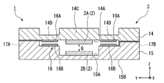
第1実施形態について説明する。図1は、第1実施形態に係る光学フィルタ装置1の一例を示す側断面図、図2は、図1の平面図である。
<First Embodiment>
A first embodiment will be described. FIG. 1 is a side sectional view showing an example of an optical filter device 1 according to the first embodiment, and FIG. 2 is a plan view of FIG.
図1及び図2において、光学フィルタ装置1は、ギャップGを介して対向する一対のミラー2(2A、2B)を有するエタロン素子3を備えている。エタロン素子3は、干渉作用により、入射した光のうち、所定波長の光(干渉光)を射出する。一方のミラー2Aと他方のミラー2Bとの間のギャップGに光が入射すると、干渉作用により、ギャップGの大きさに応じた波長の光だけがエタロン素子3より射出される。すなわち、エタロン素子3から射出される光の波長は、ギャップGの大きさに応じて変化する。
1 and 2, the optical filter device 1 includes an
エタロン素子3は、一方のミラー2Aを支持する第1基板14と、他方のミラー2Bを支持する第2基板15とを有する。第1基板14は、第2基板15と対向する表面14Aを有する。第2基板15は、第1基板14と対向する表面15Aを有する。一方のミラー2Aは、第1基板14の表面14Aの一部に配置されている。他方のミラー2Bは、第2基板15の表面15Aの一部に配置されている。第1、第2基板14、15は、光透過性である。また、本実施形態において、第1、第2基板14、15は、絶縁性である。本実施形態において、第1、第2基板14、15は、例えばガラスで形成されている。第1、第2基板14、15は、例えばソーダガラス、結晶性ガラス、石英ガラス、鉛ガラス、カリウムガラス、ホウケイ酸ガラス、ホウケイ酸ナトリウムガラス、無アルカリガラス等の各種ガラスで形成可能である。
The
本実施形態において、第1基板14は、第1部分14C及び第1部分14Cより薄い第2部分14Dを有する。厚みが薄い第2部分14Dは、弾性(可撓性)を有し、変形可能(変位可能)である。第2部分14Dが設けられることによって、第1基板14は、僅かに変形可能である。以下の説明において、第2部分14Dを適宜、ダイヤフラム部14D、と称する。第1基板14が変形することによって、Z軸方向に関する第1基板14の表面14Aと第2基板15の表面15Aとの距離が変化する。第1基板14が変形することによって、表面14Aに配置されている一方のミラー2Aと、表面15Aに配置されている他方のミラー2BとのギャップGの大きさが変化する。
In the present embodiment, the
以下の説明において、変形可能な第1基板14に支持されている一方のミラー2Aを適宜、可動ミラー2A、と称し、第2基板15に支持されている他方のミラー2Bを適宜、固定ミラー2B、と称する。
In the following description, one
また、光学フィルタ装置1は、ギャップGの大きさを調整するために、第1基板14を変形可能な駆動素子16を備えている。上述のように、ダイヤフラム部14Dを含む第1基板14は、変形可能である。第1基板14を変形させることによって、可動ミラー2Aが移動する。可動ミラー2Aが移動することによって、ギャップGの大きさが変化する。
In addition, the optical filter device 1 includes a
本実施形態において、駆動素子16は、第1、第2基板14、15に配置され、静電力を発生可能な電極16A、16Bを含む。一方の電極16Aは、第1基板14の表面14Aに配置され、他方の基板16Bは、第2基板15の表面15Aに配置される。一方の電極16Aと他方の電極16Bとは対向する。電極16Aは、表面14Aにおいて、可動ミラー2Aの周囲に配置されている。電極16Bは、表面15Aにおいて、固定ミラー2Bの周囲に配置されている。本実施形態においては、表面14A、15Aとほぼ平行なXY平面内において、電極16A、16Bは、ほぼ円環状である。
In the present embodiment, the
電極16A、16Bを形成する材料としては、導電性であれば特に限定されず、例えば、Cr、Al、Al合金、Ni、Zn、Tiなどの金属、カーボン、チタン等を分散した樹脂、多結晶シリコン(ポリシリコン)、アモルファスシリコン等のシリコン、窒化シリコン、ITOのような透明導電材料、Au等が挙げられる。
The material for forming the
電極16Aは、引き出し配線17A及び配線を介して、電源(不図示)と接続されている。電極16Bは、引き出し配線17B及び配線を介して、電源と接続されている。電源は、電極16A、16Bに電圧を印加する。電源により、電極16Aと電極16Bとの間に電位差が生じる。
The
電極16A、16Bに電圧が印加されることにより、電極16Aと電極16Bとの間に、印可される電圧(電位差)に応じた静電力が発生する。電極16A、16Bに電圧が印加され、電極16Aと電極16Bとの間に静電力が発生することによって、第1基板14が変形する。第1基板14が変形することによって、ギャップGの大きさが調整される。
When a voltage is applied to the
上述のように、エタロン素子3から射出される光の波長は、ギャップGの大きさに応じて変化する。ギャップGの大きさは、電極16Aと電極16Bとの間の電位差に基づいて電極16Aと電極16Bとの間に発生する静電力によって調整される。したがって、電極16A、16Bに印加される電圧が調整され、ギャップGの大きさが調整されることによって、エタロン素子3から射出される光の波長が調整される。本実施形態においては、エタロン素子3から射出される光が目標波長の光を含むように、電極16A、16Bに印加される電圧が調整される。
As described above, the wavelength of light emitted from the
なお、電極16A、16Bを複数設け、それら複数の電極16A、16BをXY平面内において複数の位置に配置し、各電極16A、16B間の電位差(静電力)をそれぞれ調整することによって、第2基板15に対して第1基板14を傾斜させることもできる。
A plurality of
本実施形態において、ミラー2(2A、2B)は、炭素を含有する銀の合金膜である。本実施形態においては、ミラー2は、炭素を含有する銀の合金膜で形成された単層膜である。本実施形態において、ミラー2は、銀に所定量の炭素を添加した材料で形成されている。
In the present embodiment, the mirror 2 (2A, 2B) is a silver alloy film containing carbon. In the present embodiment, the
銀は、反射率が高く、所望の反射率を有するミラー2を形成できる材料である。しかし、ミラーを純銀(銀100%)で形成すると、耐腐食性が低下する等、ミラーは十分な耐久性を得られなくなる可能性がある。また、変色等により、ミラーの反射率が低下する可能性もある。また、ミラーがガラス基板上に形成される場合において、ミラーを純銀(銀100%)で形成すると、ミラーとガラス基板との十分な密着性を得られなくなる可能性がある。
Silver is a material having a high reflectivity and capable of forming the
本実施形態によれば、エタロン素子3のミラー2が、炭素を含有する銀の合金膜なので、ミラー2の耐久性(耐腐食性)を高めることができる。また、ミラー2と第1、第2基板14、15との密着性を高めることができる。したがって、光学フィルタ装置1の性能の低下を抑制できる。
According to this embodiment, since the
本実施形態において、銀に対する炭素の含有率は、1〜30%であることが望ましく、1〜10%であることがより望ましい。これにより、所望の性能のミラー2を形成できる。炭素の含有率が1%未満の場合、ミラー2は、十分な耐久性及び密着性を得ることができない。一方、炭素の含有率が多い場合、ミラー2は、例えば所望の反射特性(反射率)が得られない等、光学性能が低下する可能性がある。炭素の含有率を1〜30%、より望ましくは1〜10%とすることによって、ミラー2は、所望の光学性能を維持しつつ、耐久性及び密着性を得ることができる。
In the present embodiment, the carbon content relative to silver is preferably 1 to 30%, and more preferably 1 to 10%. Thereby, the
以上説明したように、本実施形態によれば、エタロン素子3のミラー2が、炭素を含有する銀の合金膜を含むので、ミラー2の耐久性を高めたり、ミラー2と第1、第2基板14、15との密着性を高めたりすることができる。したがって、光学フィルタ装置1の性能の低下を抑制できる。
As described above, according to the present embodiment, since the
また、ミラー2の耐久性が向上するので、例えばエタロン素子3の製造時においても、ミラー2の劣化が抑制される。
Further, since the durability of the
<第2実施形態>
次に、第2実施形態について説明する。以下の説明において、上述の実施形態と同一又は同等の構成部分については同一の符号を付し、その説明を簡略若しくは省略する。
Second Embodiment
Next, a second embodiment will be described. In the following description, the same or equivalent components as those of the above-described embodiment are denoted by the same reference numerals, and the description thereof is simplified or omitted.
図3は、第2実施形態に係るミラー20を示す図である。図3に示すように、第2実施形態に係るミラー20は、誘電体多層膜30と、誘電体多層膜30の最も表層を覆う合金膜2Gとを有する。合金膜2Gは、炭素を含有する銀の合金膜である。合金膜2Gは、炭素を含有する銀の合金膜で形成された単層膜である。合金膜2Gは、銀に所定量の炭素を添加した材料で形成されている。本実施形態において、銀に対する炭素の含有率は、1〜30%であることが望ましく、1〜10%であることがより望ましい。
FIG. 3 is a diagram illustrating the
誘電体多層膜30は、高屈折率層31と低屈折率層32とが交互に複数積層された多層膜である。
The
エタロン素子3を可視光領域、赤外光領域で用いる場合、高屈折率層31を形成する材料として、例えばTi2O、Ta2O5、酸化ニオブ等が挙げられる。エタロン素子3を紫外光領域で用いる場合、高屈折率層31を形成する材料として、例えばAl2O3、HfO2、ZrO2、ThO2等が挙げられる。低屈折率層32を形成する材料として、例えばMgF2、SiO2等が挙げられる。
When the
高屈折率層31及び低屈折率層32の層数、厚さは、必要とする光学特性に応じて設定される。一般に、多層膜により反射膜を構成する場合、その光学特性を得るために必要な層数は12層以上であり、多層膜により反射防止膜を構成する場合、その光学特性に必要な層数は4層程度である。
The number and thickness of the high
本実施形態によれば、誘電体多層膜30の最も表層を、炭素を含有する銀の合金膜2Gで覆うので、ミラー20の耐久性(耐腐食性)を高めることができる。また、ミラー20が誘電体多層膜30を含むので、ミラー20の透過特性が向上する。また、合金膜2Gと誘電体多層膜30との密着性は良好である。したがって、光学フィルタ装置1の性能の低下を抑制できる。
According to the present embodiment, since the outermost surface of the
<第3実施形態>
次に、第3実施形態について説明する。以下の説明において、上述の実施形態と同一又は同等の構成部分については同一の符号を付し、その説明を簡略若しくは省略する。
<Third Embodiment>
Next, a third embodiment will be described. In the following description, the same or equivalent components as those of the above-described embodiment are denoted by the same reference numerals, and the description thereof is simplified or omitted.
図4は、第3実施形態に係るミラー20Bを示す図である。第3実施形態に係るミラー20Bは、第2実施形態に係るミラー20の変形例である。第2実施形態に係るミラー20と異なる第3実施形態に係るミラー20Bの特徴的な部分は、保護膜40が設けられている点にある。
FIG. 4 is a diagram showing a
図4に示すように、第2実施形態に係るミラー20Bは、誘電体多層膜30と、誘電体多層膜30の最も表層を覆う合金膜2Gと、合金膜2Gの表面を覆う保護膜40とを有する。保護膜40は、合金膜2G及び誘電体多層膜30を保護する機能を有する。保護膜40は、例えばSiO2で形成されている。保護膜40を設けることにより、より一層、ミラー20Bの耐久性が向上される。
As shown in FIG. 4, the
<実験例>
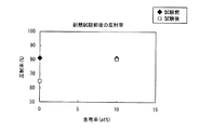
以下、炭素を含有する銀の合金膜に関して行った評価試験結果について、図5〜図8を参照して説明する。図5は、銀に対する炭素の含有率(atomic%)と、合金膜の比抵抗と、合金膜の熱伝導率との関係を示す。図6は、銀に対する炭素の含有率(atomic%)と、合金膜の反射率との関係を示す。図7は、耐久性試験として、耐塩水試験したときの、銀に対する炭素の含有率(atomic%)と、合金膜の反射率との関係を示す。図8は、耐久性試験として、耐熱試験したときの、銀に対する炭素の含有率(atomic%)と、合金膜の反射率との関係を示す。耐塩水試験は、NaClの濃度が10%の水溶液に、合金膜を1時間浸ける試験である。耐熱試験は、大気中で合金膜を250℃で1時間加熱する試験である。
<Experimental example>
Hereinafter, the result of the evaluation test performed on the silver alloy film containing carbon will be described with reference to FIGS. FIG. 5 shows the relationship between the carbon content (atomic%) relative to silver, the specific resistance of the alloy film, and the thermal conductivity of the alloy film. FIG. 6 shows the relationship between the carbon content to silver (atomic%) and the reflectance of the alloy film. FIG. 7 shows the relationship between the carbon content with respect to silver (atomic%) and the reflectance of the alloy film when the salt resistance test is performed as a durability test. FIG. 8 shows the relationship between the carbon content with respect to silver (atomic%) and the reflectance of the alloy film when subjected to a heat resistance test as a durability test. The salt water resistance test is a test in which the alloy film is immersed in an aqueous solution having a NaCl concentration of 10% for 1 hour. The heat resistance test is a test in which the alloy film is heated at 250 ° C. for 1 hour in the atmosphere.
図5は、銀に対する炭素の含有率(atomic%)と、合金膜の比抵抗と、合金膜の熱伝導率との関係を示す図であって、横軸は、銀に対する炭素の含有率であり、縦軸は、合金膜の比抵抗及び熱伝導率である。図5に示すように、炭素の含有率が多くなると、合金膜の比抵抗は上昇し、合金膜の熱伝導率は低下する。 FIG. 5 is a graph showing the relationship between the carbon content to silver (atomic%), the specific resistance of the alloy film, and the thermal conductivity of the alloy film. The horizontal axis represents the carbon content to silver. Yes, the vertical axis represents the specific resistance and thermal conductivity of the alloy film. As shown in FIG. 5, when the carbon content increases, the specific resistance of the alloy film increases and the thermal conductivity of the alloy film decreases.
炭素の含有率を30%程度に抑えることによって、合金膜の比抵抗を、約4〔μΩ・cm〕程度にすることができ、合金膜の熱伝導率を、約255〔W/m・K〕にすることができる。 By suppressing the carbon content to about 30%, the specific resistance of the alloy film can be about 4 [μΩ · cm], and the thermal conductivity of the alloy film can be about 255 [W / m · K]. ].
図6は、銀に対する炭素の含有率(atomic%)と、合金膜の反射率との関係を示す図であって、合金膜の厚みが400nmの場合と、600nmの場合とを示す。図6の横軸は、銀に対する炭素の含有率であり、縦軸は、合金膜の反射率である。図6に示すように、炭素の含有率が多くなると、合金膜の反射率が低下する。 FIG. 6 is a diagram showing the relationship between the carbon content (atomic%) with respect to silver and the reflectance of the alloy film, and shows the case where the thickness of the alloy film is 400 nm and the case of 600 nm. The horizontal axis in FIG. 6 is the carbon content relative to silver, and the vertical axis is the reflectance of the alloy film. As shown in FIG. 6, as the carbon content increases, the reflectance of the alloy film decreases.
炭素の含有率を30%程度に抑えることによって、厚みが400nmの場合の合金膜の反射率を、約70〔%〕程度にすることができ、厚みが600nmの場合の合金膜の反射率を、約85〔%〕程度にすることができる。 By suppressing the carbon content to about 30%, the reflectance of the alloy film when the thickness is 400 nm can be about 70%, and the reflectance of the alloy film when the thickness is 600 nm. , About 85%.
また、炭素の含有率を10%程度に抑えることによって、厚みが400nmの場合の合金膜の反射率を、約81〔%〕程度にすることができ、厚みが600nmの場合の合金膜の反射率を、約94〔%〕程度にすることができる。また、炭素の含有率が0〔%〕の場合の、厚みが400nmの合金膜の反射率は、約81〔%〕であり、炭素の含有率が0〔%〕の場合の、厚みが600nmの合金膜の反射率は、約95〔%〕である。このように、銀に対する炭素の含有率が10%以下の合金膜の反射率は、炭素が含有されてない純銀の膜の反射率とほぼ同等である。すなわち、炭素の含有率を10%以下にすることによって、反射率に関して、純銀の膜とほぼ同等の性能を維持することができる。 Further, by suppressing the carbon content to about 10%, the reflectance of the alloy film when the thickness is 400 nm can be about 81 [%], and the reflection of the alloy film when the thickness is 600 nm. The rate can be about 94%. In addition, when the carbon content is 0%, the alloy film having a thickness of 400 nm has a reflectance of about 81%, and when the carbon content is 0%, the thickness is 600 nm. The reflectance of the alloy film is about 95%. Thus, the reflectance of the alloy film having a carbon content of 10% or less with respect to silver is substantially equal to the reflectance of a pure silver film not containing carbon. In other words, by setting the carbon content to 10% or less, it is possible to maintain the same performance as the pure silver film with respect to the reflectance.
図7は、耐久性試験として、耐塩水試験したときの、銀に対する炭素の含有率(atomic%)と、合金膜の反射率との関係を示す図であって、合金膜を塩水に接触させる前の状態と、塩水に接触させた後の状態とを示す。図7の横軸は、銀に対する炭素の含有率であり、縦軸は、合金膜の反射率である。図7に示すように、銀に対する炭素の含有率が0〔%〕の場合、塩水に接触させる前の状態では、反射率が約81〔%〕であった合金膜が、塩水に接触させた後の状態では、反射率が約72〔%〕となり、反射率が低下することが分かる。一方、銀に対する炭素の含有率が約10〔%〕の場合、塩水に接触させる前の状態、及び塩水に接触させた後の状態のそれぞれにおいて、合金膜の反射率は、約81〔%〕である。すなわち、銀に対する炭素の含有率が0〔%〕の場合、合金膜は、十分な耐久性を得られず、塩水に接触することによって、変色(変質)し、その合金膜の反射率が低下してしまう。銀に対する炭素の含有率を約10〔%〕にした材料で合金膜を形成することによって、合金膜の耐久性が維持され、塩水に接触した場合でも、合金膜の反射率の低下が抑制される。 FIG. 7 is a diagram showing the relationship between the carbon content to silver (atomic%) and the reflectance of the alloy film when the salt resistance test is performed as a durability test. The alloy film is brought into contact with salt water. The previous state and the state after contact with salt water are shown. The horizontal axis in FIG. 7 is the carbon content relative to silver, and the vertical axis is the reflectance of the alloy film. As shown in FIG. 7, when the carbon content with respect to silver was 0%, the alloy film having a reflectance of about 81% was brought into contact with salt water before contact with the salt water. In the later state, it can be seen that the reflectance is about 72% and the reflectance is lowered. On the other hand, when the carbon content with respect to silver is about 10 [%], the reflectance of the alloy film is about 81 [%] in each of the state before contact with salt water and the state after contact with salt water. It is. That is, when the carbon content with respect to silver is 0 [%], the alloy film cannot obtain sufficient durability, and it changes color (changes in quality) by contacting with salt water, and the reflectance of the alloy film decreases. Resulting in. By forming the alloy film with a material whose carbon content with respect to silver is about 10%, the durability of the alloy film is maintained, and even when it comes into contact with salt water, the decrease in the reflectance of the alloy film is suppressed. The
図8は、耐久性試験として、耐熱試験したときの、銀に対する炭素の含有率(atomic%)と、合金膜の反射率との関係を示す図であって、合金膜を加熱する前の状態と、加熱した後の状態とを示す。図8の横軸は、銀に対する炭素の含有率であり、縦軸は、合金膜の反射率である。図8に示すように、銀に対する炭素の含有率が0〔%〕の場合、加熱する前の状態では、反射率が約81〔%〕であった合金膜が、加熱した後の状態では、反射率が約65〔%〕となり、反射率が低下することが分かる。一方、銀に対する炭素の含有率が約10〔%〕の場合、加熱する前の状態、及び加熱した後の状態のそれぞれにおいて、合金膜の反射率は、約81〔%〕である。すなわち、銀に対する炭素の含有率が0〔%〕の場合、合金膜は、十分な耐久性を得られず、加熱することによって、変色(変質)し、その合金膜の反射率が低下してしまう。銀に対する炭素の含有率を約10〔%〕にした材料で合金膜を形成することによって、合金膜の耐久性が維持され、加熱した場合でも、合金膜の反射率の低下が抑制される。 FIG. 8 is a diagram showing the relationship between the carbon content to silver (atomic%) and the reflectance of the alloy film when the heat resistance test is performed as a durability test, and the state before heating the alloy film And the state after heating. The horizontal axis in FIG. 8 is the carbon content relative to silver, and the vertical axis is the reflectance of the alloy film. As shown in FIG. 8, when the carbon content relative to silver is 0%, the alloy film having a reflectance of about 81% in the state before heating is in the state after heating, It can be seen that the reflectance is about 65% and the reflectance is lowered. On the other hand, when the carbon content with respect to silver is about 10 [%], the reflectance of the alloy film is about 81 [%] in each of the state before heating and the state after heating. That is, when the carbon content with respect to silver is 0%, the alloy film cannot obtain sufficient durability, and when heated, the alloy film is discolored (denatured), and the reflectance of the alloy film decreases. End up. By forming the alloy film with a material having a carbon content of about 10% with respect to silver, durability of the alloy film is maintained, and even when heated, a decrease in the reflectance of the alloy film is suppressed.
このように、図6〜図8の評価試験結果より、銀に対する炭素の含有率を1〜10%程度にした材料で合金膜を形成することによって、純銀の膜と同等の反射率を維持したまま、耐久性を向上することができる。 Thus, from the evaluation test results of FIGS. 6 to 8, the reflectance equivalent to that of a pure silver film was maintained by forming an alloy film with a material in which the carbon content to silver was about 1 to 10%. The durability can be improved.
1…光学フィルタ装置、2…ミラー、2A…可動ミラー、2B…固定ミラー、2G…合金膜、3…エタロン素子、30…誘電体多層膜、G…ギャップ DESCRIPTION OF SYMBOLS 1 ... Optical filter apparatus, 2 ... Mirror, 2A ... Movable mirror, 2B ... Fixed mirror, 2G ... Alloy film, 3 ... Etalon element, 30 ... Dielectric multilayer film, G ... Gap
Claims (4)
前記ミラーは、炭素を含有する銀の合金膜と誘電体多層膜とを含み、
互いに対向する前記ミラーの表面に前記合金膜が設けられており、
前記銀に対する前記炭素の含有率が、1〜30%であることを特徴とする光学フィルタ装置。 Comprising an etalon element having a pair of mirrors opposed via a gap;
The mirror includes a silver alloy film containing carbon and a dielectric multilayer film,
The alloy film is provided on the surfaces of the mirrors facing each other ;
The optical filter device , wherein a content ratio of the carbon with respect to the silver is 1 to 30% .
前記第1ミラーとギャップを介して対向し、特定の波長の光を射出し前記特定の波長の光以外の光を反射する第2ミラーと、
前記第1ミラーを移動させ前記第1ミラーと前記第2ミラーとの前記ギャップを調整する駆動素子と、を備え、
前記第1ミラー及び前記第2ミラーは、炭素を含有する銀の合金膜と誘電体多層膜とを含み、
互いに対向する前記第1ミラー及び前記第2ミラーの表面に前記合金膜が設けられており、
前記銀に対する前記炭素の含有率が、1〜30%であることを特徴とする光学フィルタ装置。 A first mirror that emits light of a specific wavelength and reflects light other than the light of the specific wavelength;
A second mirror that faces the first mirror through a gap, emits light of a specific wavelength, and reflects light other than the light of the specific wavelength;
A driving element for moving the first mirror and adjusting the gap between the first mirror and the second mirror;
The first mirror and the second mirror include a silver alloy film containing carbon and a dielectric multilayer film,
The alloy film is provided on the surfaces of the first mirror and the second mirror facing each other ,
The optical filter device , wherein a content ratio of the carbon with respect to the silver is 1 to 30% .
Priority Applications (1)
| Application Number | Priority Date | Filing Date | Title |
|---|---|---|---|
| JP2008096176A JP5564759B2 (en) | 2008-04-02 | 2008-04-02 | Optical filter device |
Applications Claiming Priority (1)
| Application Number | Priority Date | Filing Date | Title |
|---|---|---|---|
| JP2008096176A JP5564759B2 (en) | 2008-04-02 | 2008-04-02 | Optical filter device |
Publications (3)
| Publication Number | Publication Date |
|---|---|
| JP2009251105A JP2009251105A (en) | 2009-10-29 |
| JP2009251105A5 JP2009251105A5 (en) | 2011-05-12 |
| JP5564759B2 true JP5564759B2 (en) | 2014-08-06 |
Family
ID=41311920
Family Applications (1)
| Application Number | Title | Priority Date | Filing Date |
|---|---|---|---|
| JP2008096176A Expired - Fee Related JP5564759B2 (en) | 2008-04-02 | 2008-04-02 | Optical filter device |
Country Status (1)
| Country | Link |
|---|---|
| JP (1) | JP5564759B2 (en) |
Families Citing this family (22)
| Publication number | Priority date | Publication date | Assignee | Title |
|---|---|---|---|---|
| JP5428805B2 (en) * | 2009-11-30 | 2014-02-26 | セイコーエプソン株式会社 | Interference filter, optical sensor, and optical module |
| JP5434719B2 (en) * | 2010-03-19 | 2014-03-05 | セイコーエプソン株式会社 | Optical filters and analytical instruments |
| JP2012027226A (en) * | 2010-07-23 | 2012-02-09 | Seiko Epson Corp | Interference filter, optical module and analyzer |
| JP5682165B2 (en) | 2010-07-23 | 2015-03-11 | セイコーエプソン株式会社 | Interference filter, optical module, and analyzer |
| JP2012042584A (en) * | 2010-08-17 | 2012-03-01 | Seiko Epson Corp | Optical filter, optical filter module, spectrometry device, and optical device |
| JP2012042651A (en) * | 2010-08-18 | 2012-03-01 | Seiko Epson Corp | Interference filter, optical module and analyzer |
| JP5779852B2 (en) | 2010-08-25 | 2015-09-16 | セイコーエプソン株式会社 | Tunable interference filter, optical module, and optical analyzer |
| JP5707780B2 (en) | 2010-08-25 | 2015-04-30 | セイコーエプソン株式会社 | Wavelength variable interference filter, optical module, and optical analyzer |
| JP5609542B2 (en) | 2010-10-28 | 2014-10-22 | セイコーエプソン株式会社 | Light measuring device |
| JP5810512B2 (en) | 2010-11-12 | 2015-11-11 | セイコーエプソン株式会社 | Optical device |
| JP5630227B2 (en) * | 2010-11-15 | 2014-11-26 | セイコーエプソン株式会社 | Optical filter and method for manufacturing optical filter |
| JP2012108440A (en) * | 2010-11-19 | 2012-06-07 | Seiko Epson Corp | Interference filter, optical module and optical analysis device |
| JP5720200B2 (en) | 2010-11-25 | 2015-05-20 | セイコーエプソン株式会社 | Optical module and optical measuring device |
| JP5545190B2 (en) * | 2010-11-26 | 2014-07-09 | セイコーエプソン株式会社 | Method for manufacturing tunable interference filter |
| JP5673049B2 (en) * | 2010-12-08 | 2015-02-18 | セイコーエプソン株式会社 | Wavelength variable interference filter, optical module, and optical analyzer |
| JP5909850B2 (en) * | 2011-02-15 | 2016-04-27 | セイコーエプソン株式会社 | Wavelength variable interference filter, optical module, and optical analyzer |
| JP5845592B2 (en) * | 2011-02-17 | 2016-01-20 | セイコーエプソン株式会社 | Wavelength variable interference filter, optical module, and optical analyzer |
| JP5910099B2 (en) | 2012-01-18 | 2016-04-27 | セイコーエプソン株式会社 | Interference filters, optical modules and electronics |
| JP6035768B2 (en) | 2012-02-16 | 2016-11-30 | セイコーエプソン株式会社 | Interference filters, optical modules, and electronics |
| JP5983020B2 (en) | 2012-05-18 | 2016-08-31 | セイコーエプソン株式会社 | Wavelength variable interference filter, optical filter device, optical module, and electronic apparatus |
| JP6390090B2 (en) | 2013-11-19 | 2018-09-19 | セイコーエプソン株式会社 | Optical filter device, optical module, and electronic apparatus |
| JP5978506B2 (en) * | 2014-11-14 | 2016-08-24 | セイコーエプソン株式会社 | Interference filter, optical module, and analyzer |
Family Cites Families (3)
| Publication number | Priority date | Publication date | Assignee | Title |
|---|---|---|---|---|
| JPH01300202A (en) * | 1988-05-27 | 1989-12-04 | Sharp Corp | Reflector and interference device using said reflector |
| JP4059714B2 (en) * | 2002-07-04 | 2008-03-12 | Tdk株式会社 | Optical recording medium |
| JP2007002275A (en) * | 2005-06-21 | 2007-01-11 | Toyoshima Seisakusho:Kk | Material for depositing thin film, thin film deposited using the same, and method for depositing the same |
-
2008
- 2008-04-02 JP JP2008096176A patent/JP5564759B2/en not_active Expired - Fee Related
Also Published As
| Publication number | Publication date |
|---|---|
| JP2009251105A (en) | 2009-10-29 |
Similar Documents
| Publication | Publication Date | Title |
|---|---|---|
| JP5564759B2 (en) | Optical filter device | |
| JP4466634B2 (en) | Optical device, wavelength tunable filter, wavelength tunable filter module, and optical spectrum analyzer | |
| JP5682165B2 (en) | Interference filter, optical module, and analyzer | |
| JP4561728B2 (en) | Optical device, optical device manufacturing method, tunable filter, tunable filter module, and optical spectrum analyzer | |
| JP5446110B2 (en) | Receiver | |
| JP4548288B2 (en) | Tunable filter | |
| US7106514B2 (en) | Optical tunable filter and method for manufacturing the optical tunable filter | |
| JP4548245B2 (en) | Tunable filter | |
| JP4525836B2 (en) | Optical device, wavelength tunable filter, wavelength tunable filter module, and optical spectrum analyzer | |
| JP4379457B2 (en) | Optical device, wavelength tunable filter, wavelength tunable filter module, and optical spectrum analyzer | |
| JP5017803B2 (en) | Optical element and optical device | |
| JP2012042651A (en) | Interference filter, optical module and analyzer | |
| US20120019827A1 (en) | Interference filter, optical module, and analyzing device | |
| JP2012234208A (en) | Wavelength variable filter | |
| JP2013033257A (en) | Optical tunable filter | |
| JP4831245B2 (en) | Tunable filter | |
| JP4831242B2 (en) | Tunable filter | |
| JP7167455B2 (en) | Optical Scale for Encoder and Optical Encoder | |
| JP4831243B2 (en) | Tunable filter | |
| JP6052269B2 (en) | Tunable filter | |
| JP5013010B2 (en) | Tunable filter | |
| JP5751274B2 (en) | Optical device | |
| US11772363B2 (en) | Electromagnetic shielding substrate and display panel | |
| JP5824427B2 (en) | Tunable filter | |
| JP5077468B2 (en) | Tunable filter |
Legal Events
| Date | Code | Title | Description |
|---|---|---|---|
| A521 | Request for written amendment filed |
Free format text: JAPANESE INTERMEDIATE CODE: A523 Effective date: 20110323 |
|
| A621 | Written request for application examination |
Free format text: JAPANESE INTERMEDIATE CODE: A621 Effective date: 20110323 |
|
| A521 | Request for written amendment filed |
Free format text: JAPANESE INTERMEDIATE CODE: A821 Effective date: 20110324 |
|
| RD04 | Notification of resignation of power of attorney |
Free format text: JAPANESE INTERMEDIATE CODE: A7424 Effective date: 20120125 |
|
| RD03 | Notification of appointment of power of attorney |
Free format text: JAPANESE INTERMEDIATE CODE: A7423 Effective date: 20120402 |
|
| RD04 | Notification of resignation of power of attorney |
Free format text: JAPANESE INTERMEDIATE CODE: A7424 Effective date: 20120801 |
|
| A131 | Notification of reasons for refusal |
Free format text: JAPANESE INTERMEDIATE CODE: A131 Effective date: 20130528 |
|
| A521 | Request for written amendment filed |
Free format text: JAPANESE INTERMEDIATE CODE: A523 Effective date: 20130724 |
|
| A131 | Notification of reasons for refusal |
Free format text: JAPANESE INTERMEDIATE CODE: A131 Effective date: 20131029 |
|
| A521 | Request for written amendment filed |
Free format text: JAPANESE INTERMEDIATE CODE: A523 Effective date: 20131220 |
|
| TRDD | Decision of grant or rejection written | ||
| A01 | Written decision to grant a patent or to grant a registration (utility model) |
Free format text: JAPANESE INTERMEDIATE CODE: A01 Effective date: 20140520 |
|
| A61 | First payment of annual fees (during grant procedure) |
Free format text: JAPANESE INTERMEDIATE CODE: A61 Effective date: 20140602 |
|
| R150 | Certificate of patent or registration of utility model |
Ref document number: 5564759 Country of ref document: JP Free format text: JAPANESE INTERMEDIATE CODE: R150 |
|
| S531 | Written request for registration of change of domicile |
Free format text: JAPANESE INTERMEDIATE CODE: R313531 |
|
| R350 | Written notification of registration of transfer |
Free format text: JAPANESE INTERMEDIATE CODE: R350 |
|
| LAPS | Cancellation because of no payment of annual fees |