JP5427222B2 - Appearance inspection device - Google Patents
Appearance inspection device Download PDFInfo
- Publication number
- JP5427222B2 JP5427222B2 JP2011236314A JP2011236314A JP5427222B2 JP 5427222 B2 JP5427222 B2 JP 5427222B2 JP 2011236314 A JP2011236314 A JP 2011236314A JP 2011236314 A JP2011236314 A JP 2011236314A JP 5427222 B2 JP5427222 B2 JP 5427222B2
- Authority
- JP
- Japan
- Prior art keywords
- wiring board
- inspection
- light beam
- camera
- printed wiring
- Prior art date
- Legal status (The legal status is an assumption and is not a legal conclusion. Google has not performed a legal analysis and makes no representation as to the accuracy of the status listed.)
- Expired - Fee Related
Links
- 238000007689 inspection Methods 0.000 title claims description 118
- 238000003384 imaging method Methods 0.000 claims description 43
- 238000011179 visual inspection Methods 0.000 claims description 24
- 230000003287 optical effect Effects 0.000 claims description 16
- 230000001678 irradiating effect Effects 0.000 claims description 3
- 230000007246 mechanism Effects 0.000 description 11
- 230000002950 deficient Effects 0.000 description 8
- 238000012360 testing method Methods 0.000 description 7
- 229910000679 solder Inorganic materials 0.000 description 5
- 230000000007 visual effect Effects 0.000 description 5
- 230000007547 defect Effects 0.000 description 4
- 239000006071 cream Substances 0.000 description 3
- 238000005259 measurement Methods 0.000 description 3
- 238000000034 method Methods 0.000 description 3
- 239000003990 capacitor Substances 0.000 description 2
- 238000007639 printing Methods 0.000 description 2
- 238000005476 soldering Methods 0.000 description 2
- 238000009966 trimming Methods 0.000 description 2
- RYGMFSIKBFXOCR-UHFFFAOYSA-N Copper Chemical compound [Cu] RYGMFSIKBFXOCR-UHFFFAOYSA-N 0.000 description 1
- 239000004593 Epoxy Substances 0.000 description 1
- 239000011889 copper foil Substances 0.000 description 1
- 238000005516 engineering process Methods 0.000 description 1
- 238000005530 etching Methods 0.000 description 1
- 239000011521 glass Substances 0.000 description 1
- 238000005286 illumination Methods 0.000 description 1
- 230000010365 information processing Effects 0.000 description 1
- 230000001788 irregular Effects 0.000 description 1
- 238000004519 manufacturing process Methods 0.000 description 1
- 238000012986 modification Methods 0.000 description 1
- 230000004048 modification Effects 0.000 description 1
- 238000012545 processing Methods 0.000 description 1
- 238000007650 screen-printing Methods 0.000 description 1
Images


Classifications
-
- G—PHYSICS
- G01—MEASURING; TESTING
- G01N—INVESTIGATING OR ANALYSING MATERIALS BY DETERMINING THEIR CHEMICAL OR PHYSICAL PROPERTIES
- G01N21/00—Investigating or analysing materials by the use of optical means, i.e. using sub-millimetre waves, infrared, visible or ultraviolet light
- G01N21/84—Systems specially adapted for particular applications
- G01N21/88—Investigating the presence of flaws or contamination
- G01N21/95—Investigating the presence of flaws or contamination characterised by the material or shape of the object to be examined
- G01N21/956—Inspecting patterns on the surface of objects
- G01N2021/95638—Inspecting patterns on the surface of objects for PCB's
-
- H—ELECTRICITY
- H05—ELECTRIC TECHNIQUES NOT OTHERWISE PROVIDED FOR
- H05K—PRINTED CIRCUITS; CASINGS OR CONSTRUCTIONAL DETAILS OF ELECTRIC APPARATUS; MANUFACTURE OF ASSEMBLAGES OF ELECTRICAL COMPONENTS
- H05K3/00—Apparatus or processes for manufacturing printed circuits
- H05K3/30—Assembling printed circuits with electric components, e.g. with resistor
- H05K3/32—Assembling printed circuits with electric components, e.g. with resistor electrically connecting electric components or wires to printed circuits
- H05K3/34—Assembling printed circuits with electric components, e.g. with resistor electrically connecting electric components or wires to printed circuits by soldering
- H05K3/341—Surface mounted components
Landscapes
- Physics & Mathematics (AREA)
- Health & Medical Sciences (AREA)
- Life Sciences & Earth Sciences (AREA)
- Chemical & Material Sciences (AREA)
- Analytical Chemistry (AREA)
- Biochemistry (AREA)
- General Health & Medical Sciences (AREA)
- General Physics & Mathematics (AREA)
- Immunology (AREA)
- Pathology (AREA)
- Investigating Materials By The Use Of Optical Means Adapted For Particular Applications (AREA)
Description
本発明は、電子部品が実装されたプリント配線板の実装状態を検査する外観検査装置に関し、特に高密度実装された配線板の外観検査に用いて好適な外観検査装置に関する。 The present invention relates to an appearance inspection apparatus for inspecting the mounting state of a printed wiring board on which electronic components are mounted, and more particularly to an appearance inspection apparatus suitable for use in appearance inspection of a wiring board mounted with high density.
従来、プリント配線板にICやLSI、抵抗器やコンデンサ等の電子部品を実装するに際しては、近年の電子機器の小型化、高性能化、低コスト化の要請から、表面実装技術が広く用いられている。 Conventionally, when mounting electronic components such as ICs, LSIs, resistors and capacitors on printed wiring boards, surface mounting technology has been widely used due to recent demands for smaller, higher performance and lower cost electronic devices. ing.
プリント配線板に電子部品等を表面実装するに当たっては、先ず、ガラスエポキシ等のリジッドのプリント配線板にクリーム半田印刷や銅箔のエッチング等により配線パターンや電子部品が実装されるパッドが形成される。次いで、スクリーン印刷等によってパッドにクリーム半田が印刷された後、自動部品搭載機等によって所定の位置に表面実装部品を搭載し、リフロー半田付けを行う。製造後、外観検査装置によって実装状況や半田付け状況等の外観検査が行われ、また、回路の導通検査、電気的動作の機能確認が行われる。 When surface-mounting an electronic component or the like on a printed wiring board, a pad on which a wiring pattern or an electronic component is mounted is first formed on a rigid printed wiring board such as glass epoxy by cream solder printing or copper foil etching. . Next, after cream solder is printed on the pad by screen printing or the like, a surface mounting component is mounted at a predetermined position by an automatic component mounting machine or the like, and reflow soldering is performed. After the manufacturing, an appearance inspection such as a mounting state and a soldering state is performed by an appearance inspection apparatus, and a circuit continuity inspection and a function check of electrical operation are performed.
ここで、電子部品等が表面実装されたプリント配線板の外観検査では、自動検査装置による検査と目視による検査が併用され、自動検査装置による外観検査によってNGとされたプリント配線板について、目視による外観検査を行い、実装不良の態様を確認している。 Here, in the appearance inspection of the printed wiring board on which the electronic components and the like are surface-mounted, the inspection by the automatic inspection apparatus and the inspection by the visual inspection are used in combination, and the printed wiring board which is determined to be NG by the visual inspection by the automatic inspection apparatus is visually observed. Appearance inspection is performed to check the mode of mounting failure.
自動検査装置による外観検査としては、プリント配線板上部から2次元画像を撮像した撮像データと輝度データとを用いた方法、あるいはプリント配線板の3次元表面形状の計測データを用いた方法等が知られている。後者の例としては、半田実装する部品の3次元形状データに基づくマスタパターンと、部品実装後に3次元画像センサによって計測した3次元計測データとの照合を行う外観検査方法や(例えば、特許文献1参照)、クリーム半田を印刷するためのパッドを囲う検査枠を予め設定して記憶させ、部品実装後に3次元計測によって計測した半田の延出部が前記検査枠と交差するか否かによって半田ブリッジを検出する外観検査装置が知られている(例えば、特許文献2参照)。 As an appearance inspection by an automatic inspection apparatus, a method using imaging data obtained by capturing a two-dimensional image from the upper part of the printed wiring board and luminance data, or a method using measurement data of the three-dimensional surface shape of the printed wiring board is known. It has been. Examples of the latter include an appearance inspection method in which a master pattern based on three-dimensional shape data of a component to be solder-mounted is compared with three-dimensional measurement data measured by a three-dimensional image sensor after component mounting (for example, Patent Document 1). See), an inspection frame surrounding a pad for printing cream solder is set and stored in advance, and a solder bridge is determined depending on whether or not the extended portion of the solder measured by three-dimensional measurement after component mounting intersects the inspection frame. There is known an appearance inspection apparatus that detects the above (for example, see Patent Document 2).
しかし、これら自動検査装置による外観検査はいずれも推定検査であり、また、不良品の流出防止の観点から実装不良と評価する閾値を厳しく設定していることから、NGと評価されたプリント配線板が実際に実装不良を起こしているか、どのような実装不良が起きているかを目視による外観検査を行うことで確認している。目視による外観検査は、外観目視検査装置を用いて行われている。 However, these visual inspections by these automatic inspection devices are all presumed inspections, and since the threshold value for evaluating mounting defects is strictly set from the viewpoint of preventing the outflow of defective products, the printed wiring board evaluated as NG Are actually inspected by visual inspection to determine whether or not mounting defects actually occur. Visual appearance inspection is performed using an appearance visual inspection apparatus.
外観目視検査装置は、自動検査装置において実装不良とされたプリント配線板を支持する支持部と、自動検査装置において実装不良とされた特定の箇所を撮像するカメラと、カメラを実装不良とされた箇所に移動させる移動手段とを備える。カメラが撮像した画像は、外観目視検査装置と接続されたモニタに表示される。なお、カメラは、プリント配線板の法線方向から撮像する正面カメラと、プリント配線板の斜め方向から撮像する斜めカメラとを備えることで、実装不良箇所を詳細に撮像、表示することができる。 The visual appearance inspection device includes a support unit that supports a printed wiring board that has been poorly mounted in the automatic inspection device, a camera that images a specific portion that has been poorly mounted in the automatic inspection device, and a camera that is poorly mounted. Moving means for moving to a location. The image captured by the camera is displayed on a monitor connected to the visual appearance inspection device. The camera includes a front camera that captures an image from the normal direction of the printed wiring board and an oblique camera that captures an image from the oblique direction of the printed wiring board.
外観目視検査装置は、自動検査装置において特定された不良箇所の位置データを用いて予めカメラによって撮像しモニタ表示する検査ポイントを特定し、当該検査ポイントに合わせてカメラを移動させる。これにより、検査者は、モニタに表示された検査ポイントを確認することで、容易に外観検査を行うことができる。 The visual appearance inspection apparatus specifies an inspection point to be imaged and displayed in advance by a camera using position data of a defective portion specified by the automatic inspection apparatus, and moves the camera according to the inspection point. Thereby, the inspector can easily perform an appearance inspection by confirming the inspection points displayed on the monitor.
ところで、近年のプリント配線板では高密度実装の観点から基板の両面に表面実装が行われていることも多いことから、外観検査装置は、電子部品が実装されていないプリント配線板の外側縁を支持する必要がある。しかし、プリント配線板の外側縁を支持すると、プリント配線板の自重や、電子部品の重量が加わるために、反りが生じる場合がある。 By the way, in recent printed wiring boards, surface mounting is often performed on both sides of the board from the viewpoint of high-density mounting, so that the appearance inspection apparatus uses the outer edge of the printed wiring board on which electronic components are not mounted. Need to support. However, if the outer edge of the printed wiring board is supported, warpage may occur due to the weight of the printed wiring board and the weight of the electronic component.
このように外観検査装置に支持されたプリント配線板に反りが生じると、自動検査装置において特定された不良箇所と、外観目視検査装置において当該不良箇所の位置データを用いて特定された検査ポイントとの間にずれが生じ、本来確認すべき不良箇所と異なる箇所を撮像、表示するおそれがある。 When warping occurs in the printed wiring board supported by the appearance inspection device in this way, the defective portion specified in the automatic inspection device, and the inspection point specified using the position data of the defective portion in the visual appearance inspection device, There is a possibility that a difference occurs between the first and second positions, and a portion different from the defective portion to be confirmed is captured and displayed.
近年のプリント配線板では小型化された電子部品が高密度に表面実装されていることから、カメラで撮像すべき不良箇所も狭小化されているため、不良箇所と検査ポイントとがずれた場合に、実装不良を起こしている電子部品をモニタの表示から特定することは困難である。 In recent printed wiring boards, miniaturized electronic components are surface-mounted with high density, so the number of defective areas to be imaged by the camera is also narrowed, so if the defective area and the inspection point are misaligned It is difficult to identify the electronic component causing the mounting failure from the display on the monitor.
そこで、本発明は、プリント配線板に反りが生じた場合にも、検査ポイントを不良箇所に合わせて表示し、確実に外観検査を行うことができる外観検査装置を提供することを目的とする。 SUMMARY OF THE INVENTION Accordingly, an object of the present invention is to provide an appearance inspection apparatus capable of displaying an inspection point in accordance with a defective portion and performing an appearance inspection reliably even when a printed wiring board is warped.
上述した課題を解決するために、本発明に係る外観検査装置は、電子部品が実装された配線基板の外側縁を支持する支持部と、検査対象となる上記電子部品を撮像する撮像装置と、上記配線基板の法線方向に拡散して、上記配線基板の法線を含む面に存在する面をなし、検査対象となる上記電子部品について設定された要検査部位を通過する扇状の第1の光線を斜め上方から照射する第1の照射装置と、上記配線基板の法線方向に拡散して、上記配線基板の法線を含む面に存在する面をなし、上記電子部品の上記要検査部位を通過する扇状の第2の光線を斜め上方から照射する第2の照射装置とを備え、上記第1の光線と第2の光線とが交叉することにより、上記配線基板の検査ポイントを示し、上記撮像装置は、上記配線基板の法線方向から撮像する第1のカメラと、上記配線基板に対して斜め上方から撮像する第2のカメラとを備え、上記第2のカメラの光軸と上記配線基板の法線とがなす面が、上記第1の照射装置方は上記第2の照射装置のいずれかの光線とがなす面と同一平面上に位置するものである。 In order to solve the above-described problem, an appearance inspection apparatus according to the present invention includes a support unit that supports an outer edge of a wiring board on which an electronic component is mounted, an imaging device that images the electronic component to be inspected, The fan-shaped first fan that diffuses in the normal direction of the wiring board, forms a surface that exists on the surface including the normal line of the wiring board, and passes through the inspection target site set for the electronic component to be inspected. A first irradiation device that irradiates light from obliquely above; and a surface existing on a surface including the normal line of the wiring board by diffusing in a normal direction of the wiring board; A second irradiating device that irradiates the fan-shaped second light beam passing through obliquely from above, and indicates the inspection point of the wiring board by crossing the first light beam and the second light beam, The imaging device is in the normal direction of the wiring board. A first camera that captures an image and a second camera that captures an image of the wiring board obliquely from above; a surface formed by an optical axis of the second camera and a normal line of the wiring board; The first irradiation apparatus is located on the same plane as the surface formed by any one of the light beams of the second irradiation apparatus.
本発明によれば、第1の光線と第2の光線との交線は、配線基板上において光線の交点として表示され、この交点は、配線基板の反りに応じて要検査部位が昇降しても、配線基板上に映る光線の交点もZ軸に沿って追従し、常に配線基板の検査ポイントPとして指し示す。これにより、本発明によれば、照射装置によって照射される光線の交点を撮像装置によって捉えることで、確実に外観検査を行うことができる。 According to the present invention, the intersection line between the first light beam and the second light beam is displayed as the intersection of the light rays on the wiring board. However, the intersection of the light rays reflected on the wiring board also follows along the Z axis, and is always indicated as the inspection point P of the wiring board. Thereby, according to this invention, an external appearance test | inspection can be reliably performed by catching the intersection of the light ray irradiated with an irradiation apparatus with an imaging device.
以下、本発明が適用された外観検査装置について、図面を参照しながら詳細に説明する。なお、本発明は、以下の実施形態のみに限定されるものではなく、本発明の要旨を逸脱しない範囲内において種々の変更が可能であることは勿論である。 Hereinafter, an appearance inspection apparatus to which the present invention is applied will be described in detail with reference to the drawings. It should be noted that the present invention is not limited to the following embodiments, and various modifications can be made without departing from the scope of the present invention.
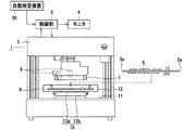
以下では、本発明を目視検査装置に適用した場合を例に説明する。この外観検査装置1は、ICやLSI、抵抗器やコンデンサ等の各種電子部品が表面実装されたプリント配線板の実装状態を目視検査するために用いられるものであり、図1、図2に示すように、箱状の外筐体2を備え、図示しないPC等の制御部3によって制御される。また、外観検査装置1は、モニタ4と接続され、撮像した画像をモニタ4に表示し、検査者による目視検査が可能とされている。
Below, the case where this invention is applied to a visual inspection apparatus is demonstrated to an example. This
[外筐体]
外観検査装置1は、外筐体2内に、プリント配線板5を支持する支持部6と、支持部6に支持されたプリント配線板の検査ポイントを撮像する撮像装置7と、プリント配線板の検査ポイントを示すレーザ照射装置8と、装置全体の動作を制御する制御部3とを備える。
[Outer housing]
The
外筐体2は、正面側が開口され、床面11上に設けられている支持部6にプリント配線板5を出し入れ可能とされている。また、外筐体2は、上側に撮像装置7が配設され、また、側方にレーザ照射装置8が配設されている。さらに、外筐体2は、内部を照明する図示しない照明手段が設けられている。
The
[支持部]
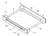
支持部6は、プリント配線板5の外側縁5aを支持する支持フレーム12と、支持フレーム12を床面11の面内方向において移動させ、プリント配線板5と撮像装置7との相対位置を移動させるステージ機構13とを備える。
[Supporting part]
The
支持フレーム12は、図3に示すように、プリント配線板5の長辺を支持する一対の長辺フレーム12a,12bと、長辺フレーム12a,12bの各両端側に設けられたコーナブロック14とを有する。支持フレーム12は、2対のコーナブロック14がそれぞれ連結バー15で連結されている。また、長辺フレーム12a,12bの背面には長辺プレート16a,16bが配設されている。外筐体2の前面側に設けられた長辺プレート16aには、長手方向に沿ってスリット17が形成され、プリント配線基板5の位置決めを行う固定ピン18が挿通されている。
As shown in FIG. 3, the
長辺フレーム12a,12bは、相対向してプリント配線板5の下面を支持する支持面が張り出し形成され、これによりプリント配線板5の外側縁5aを支持する。また、支持フレーム12は、外筐体2の背面側の長辺フレーム12bが、両側のコーナブロックが連結バー15に沿って前後方向にスライドすることで、外筐体2の前面側の長辺フレーム12aに対して近接離間可能とされ、また、固定ピン18をスリット17に沿ってスライドさせることによりプリント配線板5を左側のコーナブロック14に当接させることで、あらゆるサイズのプリント配線板5を支持することができる。
The
支持フレーム12は、プリント配線板5の電子部品が実装されていない外側縁5aを下側から支持することにより、両面実装されたプリント配線板5についても、下面の実装部品に付加をかけることなく支持することができる。
The
ステージ機構13は、支持フレーム12を一体に支持するX軸テーブル13aと、X軸テーブルをY方向へ移動可能に支持するYテーブル13bとを備える。X軸テーブル13aおよびY軸テーブル13bは、制御信号に基づいて動作するモータを備えており、これらモータを駆動することによりX軸テーブル13aがX方向へ、Y軸テーブル13bがY方向へ、支持フレーム12を一体に移動させる。
The
[撮像装置]
支持フレーム12に支持されたプリント配線板5の実装不良箇所を撮像する撮像装置7は、外筐体2の上側で支持されることにより、実装不良箇所を上側から撮像するものである。撮像装置7は、図4に示すように、カメラ光軸を支持フレーム12に支持されたプリント配線板5の法線方向に向けた正面用カメラ20と、カメラ光軸をプリント配線板5に対して斜めに傾けた斜め用カメラ21とを備える。正面用カメラ20及び斜め用カメラ21は、それぞれレンズ鏡筒内に所定の撮像レンズ及び撮像素子が組み込まれている。
[Imaging device]
The
撮像装置7は、斜め用カメラ21が正面用カメラ20を介して反対側に設けられ、これら正面用カメラ20及び斜め用カメラ21が装置本体7a内で一体化されることによりカメラユニットを構成する。また、撮像装置7は、正面用カメラ20の光軸α1を中心に回転可能とされ、斜め用カメラ21によって、あらゆる方角から実装不良箇所を撮像可能とされている。
The
なお、撮像装置7は、正面用カメラ20、斜め用カメラ21にフォーカス機能やズーム機能を備えてもよく、あるいは、これらの機能を備えず、深い被写界深度を実現するための焦点距離と絞りを有し、パンフォーカス撮影が可能なカメラを用いて撮影を行い、制御部3の処理によって適切な画像サイズで表示するようにしてもよい。
Note that the
撮像装置7は、後述するレーザ照射装置8によって示されたレーザ光の交点を検査ポイントPとして撮像できるように、レーザ照射装置8によって形成される交線Lの延長線上に予め正面用カメラ20の光軸α1が一致するとともに、斜め用カメラ21の光軸α2が当該交線L上を通過するように設計されている。
The
なお、撮像装置7は、斜め用カメラ21を複数設けてもよい。例えば、撮像装置7は、高倍率カメラと低倍率カメラとからなる1対の斜め用カメラ21を設けることにより、検査箇所に応じて使い分けることができる。また、撮像装置7は、複数の斜め用カメラ21を正面要カメラ20の光軸α1の光軸周りに、等間隔で配置してもよく又は不等間隔で配置してもよい。
Note that the
[レーザ照射装置]
次いで、支持フレーム12に支持されたプリント配線板5の検査ポイントを指し示すレーザ光を照射するレーザ照射装置8について説明する。レーザ照射装置8は、可視光レーザを照射する装置であり、撮像装置7の装置本体7a内に、互いに交叉する扇状のレーザ光を斜め上方からプリント配線板5上に照射する第1、第2のレーザ照射装置8a,8bを備える。第1、第2のレーザ照射装置8a,8bは、装置本体7a内において、照射するレーザ光が互いに直交するように配置されることが好ましい。
[Laser irradiation equipment]
Next, the
第1のレーザ照射装置8aは、自動検査装置30で予めプリント配線板5上に設定された要検査部位を通過する第1のレーザ光を照射する。同様に、第2のレーザ照射装置8bは、予めプリント配線板5上に設定された要検査部位を通過する第2のレーザ光を照射する。第1、第2のレーザ光は、いずれも支持フレーム12に支持されたプリント配線板5の法線方向に拡散する扇状の光線であり、互いに交叉することにより、プリント配線板5上に検査ポイントPを交点として指し示す。
The first
検査ポイントPは、外観検査装置1による目視検査に先立って行われた自動検査装置30による検査によって、実装不良が疑われる要検査部位が特定され、この要検査部位の位置データに基づいて、支持フレーム12に支持されたプリント配線板5上に設定された目視検査が必要な箇所をいう。撮像装置7は、この検査ポイントPを撮像するように、予め第1、第2のレーザ光の交線L上に正面用カメラ20の光軸α1を一致させる位置に設けられ、支持フレーム12は、要検査部位の位置データを参照して、第1、第2のレーザ光の交線L上に要検査部位が位置するようにステージ機構13によって移動される。
The inspection point P is determined based on the position data of the inspection required part by specifying the inspection required part where the mounting defect is suspected by the inspection by the
ここで、図6(a)に示すように、プリント配線板5に反りが生じていなければ、自動検査装置30によって設定された要検査部位の位置データに基づいてプリント配線板5と撮像装置7との相対位置を設定することで、斜め用カメラ21で目視検査が必要な検査ポイントPを捉えることができる。しかし、図6(b)に示すように、支持フレーム12に支持されたプリント配線板5に下反りが生じた場合、あるいは図6(c)に示すように、支持フレーム12に支持されたプリント配線板5に上反りが生じた場合、自動検査装置30において特定された要検査部位と、自動検査装置30によって設定された要検査部位の位置データに基づいて外観検査装置1において支持フレーム12に支持されたプリント配線板5と撮像装置7との相対位置を設定すると、モニタ4に表示される斜め用カメラ21の画像と実際の要検査部位との間にずれが生じる。
Here, as shown in FIG. 6A, if the printed
図6(c)では、プリント配線基板5が上反りしたために、斜め用カメラ21の光軸α2は、要検査部位の手前を捉え、図6(b)では、プリント配線基板5が下反りしたために、斜め用カメラ21の光軸α2は、要検査部位の先を捉えている。このように、自動検査装置30によって設定された要検査部位のデータに基づいてプリント配線板5と撮像装置7との相対位置を設定したのでは、目視検査が必要な検査ポイントPを捉えることができず、検査者は、どの表面実装部品のどの位置を目視すればよいのか判らなくなる。特に近年では、表面実装部品として、0603チップ等の一辺が1mmに満たない極小のチップ部品が用いられ、これら極小チップが高密度に実装されることから、モニタ上で検査ポイントPを確認することが困難となる。
In FIG. 6 (c), to the printed
そこで、外観検査装置1では、レーザ照射装置8によって、自動検査装置30によって設定された要検査部位のデータに基づいて設定された当該要検査部位を通過するレーザ光を照射する。このレーザ光は、プリント配線板5の法線方向に拡散する扇状の光線であり、互いに交叉することにより、互いの交線Lがプリント配線板5の要検査部位を通過する法線方向のZ軸を形成する(図5)。
Therefore, in the
この交線Lは、プリント配線板5上においてレーザ光の交点として表示され、この交点は、図7に示すように、プリント配線板5の反りに応じて要検査部位が昇降しても、プリント配線板5上に映るレーザ光の交点もZ軸に沿って追従し、常にプリント配線板5の検査ポイントPとして指し示す。これにより、外観検査装置1によれば、レーザ照射装置8によって照射されるレーザ光の交点を撮像装置7によって捉えるようにすることで、確実に検査ポイントPを撮像し、モニタに表示させることができる。
This intersection line L is displayed on the printed
[制御部]
制御部3は、検査者の操作に応じて外観検査装置1の各部を制御することにより目視検査を実行させるものであり、例えばPC等の情報処理端末を用いて構成することができる。制御部3は、自動検査装置30より、目視検査の対象となったプリント配線板5の要検査部位の位置データを受け取る。そして、制御部3は、当該位置データに基づき、レーザ照射装置8の第1、第2のレーザ照射装置8a,8bの各レーザ光の交線上に要検査部位が位置するように、ステージ機構13を駆動し支持フレーム12の位置を調整する。
[Control unit]
The
これにより、プリント配線板5に反りが生じ、要検査部位が反りに応じて上下方向に移動した場合にも、第1、第2のレーザ照射装置8a,8bの各レーザ光の交点は各レーザ光の交線Lに沿って、すなわちプリント配線板5の法線方向に沿って移動するため、常にプリント配線板5の要検査部位を検査ポイントPとして指し示すことができる。
As a result, even when the printed
次いで、制御部3は、撮像装置7の正面カメラ20及び斜め用カメラ21でプリント配線板5の要検査部位を撮像し、モニタ4に撮像装置7によって撮像された画像を表示する。この画像には、検査ポイントPとして、第1、第2のレーザ照射装置8a,8bの各レーザ光の交点が表示されているため、検査者は、この交点を目印に容易に要検査部位の検査を行うことができる。
Next, the
また、制御部3は、モニタ4の中心に、検査ポイントPを表示するようにしてもよい。すなわち、プリント配線板5が撓むことにより、要検査部位が上下方向に移動することにより、撮像装置7の撮像画像においても、図7に示すように、要検査部位を示す検査ポイントPがモニタ4上において中心からずれることがあり、反りが大きい場合などはモニタ4に表示されなくなるおそれもある。
Further, the
そこで、制御部3は、図8に示すように、第1、第2のレーザ照射装置8a,8bの各レーザ光の交点をモニタ4の中心にくるように制御することで、目視検査の利便性を向上させることができる。この制御は、例えば、撮像装置7によってパンフォーカス撮影された原画像のトリミング範囲を、第1、第2のレーザ照射装置8a,8bの各レーザ光の交点を中心に設定し所定の画像サイズでモニタ4表示することにより行うことができる。あるいは、この制御は、撮像装置7の斜め用カメラ21に、画角の調節機能と、第1、第2のレーザ照射装置8a,8bの各レーザ光の交点を探索、検知する機能とを与え、当該レーザ光の交点を中心に撮像することにより行うこともできる。
Therefore, as shown in FIG. 8, the
このとき、外観検査装置1は、図4に示すように、斜め用カメラ21と第1又は第2のレーザ照射装置8a,8bの一方とを同一方向に向けて、あるいは対向して配置し、斜め用カメラ21の光軸α2とプリント配線板5の法線とがなす面S1と、プリント配線板5の法線方向に拡散する第1又は第2のレーザ照射装置8a,8bの一方のレーザ光がなす面S2とが同一平面上に位置するようにしてもよい。
At this time, as shown in FIG. 4, the
これにより、図8に示すように、当該第1又は第2のレーザ照射装置8a,8bの一方が照射するレーザ光は、モニタ4に表示される斜め用カメラ21の画像において上下方向に照射されY軸を構成する。また、第1又は第2のレーザ照射装置8a,8bの他方が照射するレーザ光は、モニタ4に表示される斜め用カメラ21の画像において左右方向に照射されX軸を構成する。したがって、検査ポイントPも当該Y軸上に位置することとなり、モニタ4の中心に検査ポイントPを位置させるに際しては、Y軸に沿って、斜め用カメラ21の画像トリミング範囲の調整、あるいは斜め用カメラ21の画角調整を行うことができ、調整を容易に行うことができる。
Thereby, as shown in FIG. 8, the laser light emitted by one of the first or second
[他の構成]
なお、上述した外観検査装置1では、支持部6に支持フレーム12をXY方向に移動させるステージ機構13を設けることとしたが、本発明は、撮像装置7にX、Y、Z方向の移動機構を設け、プリント配線板5と撮像装置7との相対位置を移動させるようにしてもよい。
[Other configurations]
In the
また、上述した外観検査装置1では、レーザ照射装置8の第1、第2のレーザ照射装置8a,8bの各レーザ光の交線と撮像装置7の正面用カメラ20の光軸とが一致するように予め両者の位置を固定し、支持部6をXY方向に移動させて、要検査部位をレーザ光の交線上に位置させていたが、本発明は、レーザ照射装置8及び撮像装置7が組み込まれた装置本体7aにX、Y、Z方向の移動機構を設けてもよい。
In the
さらに、上述した外観検査装置1では、装置本体7a内に撮像装置及びレーザ照射装置8を組み込みユニット化したが、本発明は、撮像装置7とレーザ照射装置8とを別々に構成し外筐体2に組み込んでもよい。
Further, in the
この場合、レーザ照射装置8として、各レーザ光が直交するように第1のレーザ照射装置8a及び第2のレーザ照射装置8bを配置した場合、一方にX方向及びZ方向の移動機構を設け、他方にY方向及びZ方向の移動機構を設けてもよい。第1のレーザ照射装置8a及び第2のレーザ照射装置8bは、それぞれZ方向の移動機構を設けることにより、レーザの照射角度を調整することができる。したがって、要検査部位との間に高さのある電子部品が搭載され、これによりレーザ光が遮光される場合にも、照射位置を上げることによりレーザ光を要検査部位に照射することができる。
In this case, as the
また、この場合、斜め用カメラ21の光軸α2と第1又は第2のレーザ照射装置8a,8bの一方のレーザ光がなす面S2とが同一平面上に位置させる配置は、撮像装置7を正面用カメラ20の光軸を中心に回転させることで容易に構成することができる。
In this case, the arrangement in which the optical axis alpha 2 and the first or second
また、上記では本発明に係る外観検査装置を、目視検査装置に適用した場合を例に説明したが、本発明は、自動検査装置に適用してもよい。この場合も、要検査部位を第1、第2のレーザ照射装置8a、8bの各レーザ光の交点として示し、この交点を検出し斜め用カメラ21で撮像するように制御することで、確実に要検査部位を捉え、この撮像画像や位置データを目視検査に供することができる。
Moreover, although the case where the appearance inspection apparatus according to the present invention is applied to a visual inspection apparatus has been described above as an example, the present invention may be applied to an automatic inspection apparatus. In this case as well, it is ensured that the site to be inspected is shown as an intersection of the laser beams of the first and second
1 外観目視検査装置、2 外筐体、3 制御部、4 モニタ、5 プリント配線板、6 支持部、7 撮像装置、8 レーザ照射装置、11 床面、12 支持フレーム、13 ステージ機構、20 正面用カメラ、21 斜め用カメラ、30 自動検査装置
DESCRIPTION OF
Claims (8)
検査対象となる上記電子部品を撮像する撮像装置と、
上記配線基板の法線方向に拡散して、上記配線基板の法線を含む面に存在する面をなし、検査対象となる上記電子部品について設定された要検査部位を通過する扇状の第1の光線を斜め上方から照射する第1の照射装置と、
上記配線基板の法線方向に拡散して、上記配線基板の法線を含む面に存在する面をなし、上記電子部品の上記要検査部位を通過する扇状の第2の光線を斜め上方から照射する第2の照射装置とを備え、
上記第1の光線と第2の光線とが交叉することにより、上記配線基板の検査ポイントを示し、
上記撮像装置は、上記配線基板の法線方向から撮像する第1のカメラと、上記配線基板に対して斜め上方から撮像する第2のカメラとを備え、
上記第2のカメラの光軸と上記配線基板の法線とがなす面が、上記第1の照射装置方は上記第2の照射装置のいずれかの光線とがなす面と同一平面上に位置する外観検査装置。 A support portion for supporting the outer edge of the wiring board on which the electronic component is mounted;
An imaging device for imaging the electronic component to be inspected;
The fan-shaped first fan that diffuses in the normal direction of the wiring board, forms a surface that exists on the surface including the normal line of the wiring board, and passes through the inspection target site set for the electronic component to be inspected. A first irradiating device that irradiates light rays obliquely from above;
Diffusing in the normal direction of the wiring board, forming a surface existing on the surface including the normal line of the wiring board, and irradiating the fan-shaped second light beam passing through the inspection target site of the electronic component from diagonally above And a second irradiation device that
By crossing the first light beam and the second light beam, an inspection point of the wiring board is indicated,
The imaging apparatus includes a first camera that captures an image from a normal direction of the wiring board, and a second camera that captures an image of the wiring board from obliquely above,
The surface formed by the optical axis of the second camera and the normal line of the wiring board is located on the same plane as the surface formed by any one of the light beams of the second irradiation device in the first irradiation device. Appearance inspection device.
上記第1の光線と上記第2の光線との交点を上記モニタの中心に合わせて表示するように上記モニタ画像を制御する制御手段とを備える請求項1記載の外観検査装置。 A monitor that captures an image captured by the imaging device;
The visual inspection apparatus according to claim 1, further comprising a control unit configured to control the monitor image so as to display an intersection of the first light beam and the second light beam in accordance with a center of the monitor.
Priority Applications (3)
| Application Number | Priority Date | Filing Date | Title |
|---|---|---|---|
| JP2011236314A JP5427222B2 (en) | 2011-10-27 | 2011-10-27 | Appearance inspection device |
| CN201280038252.2A CN103718027B (en) | 2011-10-27 | 2012-10-22 | Appearance inspection device |
| PCT/JP2012/077245 WO2013061927A1 (en) | 2011-10-27 | 2012-10-22 | Appearance inspection device |
Applications Claiming Priority (1)
| Application Number | Priority Date | Filing Date | Title |
|---|---|---|---|
| JP2011236314A JP5427222B2 (en) | 2011-10-27 | 2011-10-27 | Appearance inspection device |
Publications (3)
| Publication Number | Publication Date |
|---|---|
| JP2013092508A JP2013092508A (en) | 2013-05-16 |
| JP2013092508A5 JP2013092508A5 (en) | 2013-06-27 |
| JP5427222B2 true JP5427222B2 (en) | 2014-02-26 |
Family
ID=48167758
Family Applications (1)
| Application Number | Title | Priority Date | Filing Date |
|---|---|---|---|
| JP2011236314A Expired - Fee Related JP5427222B2 (en) | 2011-10-27 | 2011-10-27 | Appearance inspection device |
Country Status (3)
| Country | Link |
|---|---|
| JP (1) | JP5427222B2 (en) |
| CN (1) | CN103718027B (en) |
| WO (1) | WO2013061927A1 (en) |
Families Citing this family (3)
| Publication number | Priority date | Publication date | Assignee | Title |
|---|---|---|---|---|
| KR101893831B1 (en) * | 2016-10-20 | 2018-08-31 | 주식회사 고영테크놀러지 | Board inspection apparatus and board inspection method using the same |
| CN108801921A (en) * | 2018-08-02 | 2018-11-13 | 佛山市坦斯盯科技有限公司 | A kind of CIS cameras and light source module group for wiring board |
| KR102693683B1 (en) * | 2020-10-05 | 2024-08-12 | 야마하하쓰도키 가부시키가이샤 | Substrate work device |
Family Cites Families (8)
| Publication number | Priority date | Publication date | Assignee | Title |
|---|---|---|---|---|
| US4240750A (en) * | 1978-10-02 | 1980-12-23 | Hurd William A | Automatic circuit board tester |
| JPH0739996B2 (en) * | 1988-09-02 | 1995-05-01 | 日本電気株式会社 | Soldering inspection device |
| JPH06331563A (en) * | 1993-05-19 | 1994-12-02 | Matsushita Electric Ind Co Ltd | Visual checker |
| JP2002312766A (en) * | 2001-04-17 | 2002-10-25 | Mitsubishi Electric Corp | Soldering state inspection device |
| US7492449B2 (en) * | 2004-04-12 | 2009-02-17 | Georgia Tech Research Corporation | Inspection systems and methods |
| US7486274B2 (en) * | 2005-08-18 | 2009-02-03 | Mitsubishi Electric Research Laboratories, Inc. | Method for stabilizing and precisely locating pointers generated by handheld direct pointing devices |
| JP2009153119A (en) * | 2007-11-30 | 2009-07-09 | Sanyo Electric Co Ltd | Imaging/video auxiliary device and imaging/video apparatus with same |
| JP2010139461A (en) * | 2008-12-15 | 2010-06-24 | Toppan Printing Co Ltd | Visual inspection system |
-
2011
- 2011-10-27 JP JP2011236314A patent/JP5427222B2/en not_active Expired - Fee Related
-
2012
- 2012-10-22 WO PCT/JP2012/077245 patent/WO2013061927A1/en active Application Filing
- 2012-10-22 CN CN201280038252.2A patent/CN103718027B/en not_active Expired - Fee Related
Also Published As
| Publication number | Publication date |
|---|---|
| CN103718027B (en) | 2015-12-23 |
| JP2013092508A (en) | 2013-05-16 |
| WO2013061927A1 (en) | 2013-05-02 |
| CN103718027A (en) | 2014-04-09 |
Similar Documents
| Publication | Publication Date | Title |
|---|---|---|
| JP5221604B2 (en) | X-ray inspection equipment | |
| KR101245148B1 (en) | Vision inspect apparatus of improved picture visibility | |
| KR20090110495A (en) | Vision inspection system | |
| JPH10300448A (en) | Device and method for inspection of printed circuit board assembly | |
| JP4877100B2 (en) | Mounting board inspection apparatus and inspection method | |
| JP2005140584A (en) | Three-dimensional measuring device | |
| KR101144749B1 (en) | Method for inspecting joint error of an element formed on a printed circuit board | |
| KR20120052087A (en) | Method of inspecting board | |
| KR101245622B1 (en) | Vision inspection apparatus using stereo vision grid pattern | |
| CN107110789B (en) | Method and apparatus for inspecting component-mounted substrate | |
| JP5427222B2 (en) | Appearance inspection device | |
| JP5421409B2 (en) | Appearance inspection apparatus and appearance inspection method | |
| KR101693614B1 (en) | Jig for X-ray Examination | |
| JP4030726B2 (en) | Solder printing inspection device | |
| JP6347962B2 (en) | Appearance inspection apparatus, appearance inspection method, and program | |
| KR20150108634A (en) | Digital light processing projector for printed circuit board inspection | |
| KR101032142B1 (en) | Surface Mounter Part Of Testing Device | |
| CN114667445A (en) | Inspection system | |
| KR20110120461A (en) | Vision inspection apparatus | |
| KR100955815B1 (en) | Automatic optical inspection apparatus | |
| JP4034325B2 (en) | Three-dimensional measuring device and inspection device | |
| JP5488179B2 (en) | Inspection apparatus and inspection method | |
| KR101282020B1 (en) | Macro type device for inspecting substrate | |
| JP2005101084A (en) | Method and device for part float check | |
| JP2005233971A (en) | X-ray fluoroscopic imaging equipment |
Legal Events
| Date | Code | Title | Description |
|---|---|---|---|
| A521 | Request for written amendment filed |
Free format text: JAPANESE INTERMEDIATE CODE: A523 Effective date: 20130313 |
|
| A621 | Written request for application examination |
Free format text: JAPANESE INTERMEDIATE CODE: A621 Effective date: 20130313 |
|
| A871 | Explanation of circumstances concerning accelerated examination |
Free format text: JAPANESE INTERMEDIATE CODE: A871 Effective date: 20130313 |
|
| A975 | Report on accelerated examination |
Free format text: JAPANESE INTERMEDIATE CODE: A971005 Effective date: 20130625 |
|
| A131 | Notification of reasons for refusal |
Free format text: JAPANESE INTERMEDIATE CODE: A131 Effective date: 20130702 |
|
| A521 | Request for written amendment filed |
Free format text: JAPANESE INTERMEDIATE CODE: A523 Effective date: 20130726 |
|
| A521 | Request for written amendment filed |
Free format text: JAPANESE INTERMEDIATE CODE: A523 Effective date: 20130805 |
|
| TRDD | Decision of grant or rejection written | ||
| A01 | Written decision to grant a patent or to grant a registration (utility model) |
Free format text: JAPANESE INTERMEDIATE CODE: A01 Effective date: 20131112 |
|
| A61 | First payment of annual fees (during grant procedure) |
Free format text: JAPANESE INTERMEDIATE CODE: A61 Effective date: 20131129 |
|
| R150 | Certificate of patent or registration of utility model |
Free format text: JAPANESE INTERMEDIATE CODE: R150 Ref document number: 5427222 Country of ref document: JP Free format text: JAPANESE INTERMEDIATE CODE: R150 |
|
| R250 | Receipt of annual fees |
Free format text: JAPANESE INTERMEDIATE CODE: R250 |
|
| R250 | Receipt of annual fees |
Free format text: JAPANESE INTERMEDIATE CODE: R250 |
|
| R250 | Receipt of annual fees |
Free format text: JAPANESE INTERMEDIATE CODE: R250 |
|
| R250 | Receipt of annual fees |
Free format text: JAPANESE INTERMEDIATE CODE: R250 |
|
| R250 | Receipt of annual fees |
Free format text: JAPANESE INTERMEDIATE CODE: R250 |
|
| R250 | Receipt of annual fees |
Free format text: JAPANESE INTERMEDIATE CODE: R250 |
|
| LAPS | Cancellation because of no payment of annual fees |