JP5426307B2 - Glass substrate for magnetic disk and magnetic disk - Google Patents
Glass substrate for magnetic disk and magnetic disk Download PDFInfo
- Publication number
- JP5426307B2 JP5426307B2 JP2009228169A JP2009228169A JP5426307B2 JP 5426307 B2 JP5426307 B2 JP 5426307B2 JP 2009228169 A JP2009228169 A JP 2009228169A JP 2009228169 A JP2009228169 A JP 2009228169A JP 5426307 B2 JP5426307 B2 JP 5426307B2
- Authority
- JP
- Japan
- Prior art keywords
- glass substrate
- magnetic disk
- main surface
- magnetic
- glass
- Prior art date
- Legal status (The legal status is an assumption and is not a legal conclusion. Google has not performed a legal analysis and makes no representation as to the accuracy of the status listed.)
- Active
Links
- 239000000758 substrate Substances 0.000 title claims description 240
- 239000011521 glass Substances 0.000 title claims description 234
- 230000007547 defect Effects 0.000 claims description 111
- 230000003746 surface roughness Effects 0.000 claims description 18
- 230000001678 irradiating effect Effects 0.000 claims description 7
- CPBQJMYROZQQJC-UHFFFAOYSA-N helium neon Chemical compound [He].[Ne] CPBQJMYROZQQJC-UHFFFAOYSA-N 0.000 claims description 5
- 239000010410 layer Substances 0.000 description 81
- 238000005498 polishing Methods 0.000 description 77
- 238000004140 cleaning Methods 0.000 description 59
- 238000000034 method Methods 0.000 description 54
- 238000007517 polishing process Methods 0.000 description 28
- KFZMGEQAYNKOFK-UHFFFAOYSA-N Isopropanol Chemical compound CC(C)O KFZMGEQAYNKOFK-UHFFFAOYSA-N 0.000 description 27
- 238000003426 chemical strengthening reaction Methods 0.000 description 25
- 230000008569 process Effects 0.000 description 25
- 239000007788 liquid Substances 0.000 description 23
- KRKNYBCHXYNGOX-UHFFFAOYSA-N citric acid Chemical compound OC(=O)CC(O)(C(O)=O)CC(O)=O KRKNYBCHXYNGOX-UHFFFAOYSA-N 0.000 description 21
- 239000005357 flat glass Substances 0.000 description 20
- 239000002253 acid Substances 0.000 description 18
- 238000000227 grinding Methods 0.000 description 18
- 238000004519 manufacturing process Methods 0.000 description 17
- 239000000463 material Substances 0.000 description 17
- 239000006061 abrasive grain Substances 0.000 description 16
- 239000000654 additive Substances 0.000 description 16
- 239000002002 slurry Substances 0.000 description 16
- 230000000996 additive effect Effects 0.000 description 15
- QAOWNCQODCNURD-UHFFFAOYSA-N Sulfuric acid Chemical compound OS(O)(=O)=O QAOWNCQODCNURD-UHFFFAOYSA-N 0.000 description 14
- 239000005354 aluminosilicate glass Substances 0.000 description 13
- 239000002245 particle Substances 0.000 description 13
- 238000007689 inspection Methods 0.000 description 11
- 230000002093 peripheral effect Effects 0.000 description 11
- 238000012545 processing Methods 0.000 description 11
- XLYOFNOQVPJJNP-UHFFFAOYSA-N water Substances O XLYOFNOQVPJJNP-UHFFFAOYSA-N 0.000 description 11
- 239000000203 mixture Substances 0.000 description 10
- QTBSBXVTEAMEQO-UHFFFAOYSA-N Acetic acid Chemical compound CC(O)=O QTBSBXVTEAMEQO-UHFFFAOYSA-N 0.000 description 9
- 230000000052 comparative effect Effects 0.000 description 9
- 238000012360 testing method Methods 0.000 description 9
- 239000011241 protective layer Substances 0.000 description 7
- MUBZPKHOEPUJKR-UHFFFAOYSA-N Oxalic acid Chemical compound OC(=O)C(O)=O MUBZPKHOEPUJKR-UHFFFAOYSA-N 0.000 description 6
- 229910004298 SiO 2 Inorganic materials 0.000 description 6
- 150000007513 acids Chemical class 0.000 description 6
- -1 aminotrimethylene phosphonic acids Chemical class 0.000 description 6
- 229910000420 cerium oxide Inorganic materials 0.000 description 6
- 230000001050 lubricating effect Effects 0.000 description 6
- 238000005259 measurement Methods 0.000 description 6
- 230000007246 mechanism Effects 0.000 description 6
- 230000003287 optical effect Effects 0.000 description 6
- BMMGVYCKOGBVEV-UHFFFAOYSA-N oxo(oxoceriooxy)cerium Chemical compound [Ce]=O.O=[Ce]=O BMMGVYCKOGBVEV-UHFFFAOYSA-N 0.000 description 6
- IJGRMHOSHXDMSA-UHFFFAOYSA-N Atomic nitrogen Chemical compound N#N IJGRMHOSHXDMSA-UHFFFAOYSA-N 0.000 description 4
- DHMQDGOQFOQNFH-UHFFFAOYSA-N Glycine Chemical compound NCC(O)=O DHMQDGOQFOQNFH-UHFFFAOYSA-N 0.000 description 4
- AEMRFAOFKBGASW-UHFFFAOYSA-N Glycolic acid Chemical compound OCC(O)=O AEMRFAOFKBGASW-UHFFFAOYSA-N 0.000 description 4
- OFOBLEOULBTSOW-UHFFFAOYSA-N Malonic acid Chemical compound OC(=O)CC(O)=O OFOBLEOULBTSOW-UHFFFAOYSA-N 0.000 description 4
- VYPSYNLAJGMNEJ-UHFFFAOYSA-N Silicium dioxide Chemical compound O=[Si]=O VYPSYNLAJGMNEJ-UHFFFAOYSA-N 0.000 description 4
- FKNQFGJONOIPTF-UHFFFAOYSA-N Sodium cation Chemical compound [Na+] FKNQFGJONOIPTF-UHFFFAOYSA-N 0.000 description 4
- 239000008119 colloidal silica Substances 0.000 description 4
- 238000005520 cutting process Methods 0.000 description 4
- 229910003460 diamond Inorganic materials 0.000 description 4
- 239000010432 diamond Substances 0.000 description 4
- 238000005342 ion exchange Methods 0.000 description 4
- FGIUAXJPYTZDNR-UHFFFAOYSA-N potassium nitrate Chemical compound [K+].[O-][N+]([O-])=O FGIUAXJPYTZDNR-UHFFFAOYSA-N 0.000 description 4
- 238000003825 pressing Methods 0.000 description 4
- 239000011347 resin Substances 0.000 description 4
- 229920005989 resin Polymers 0.000 description 4
- 239000005361 soda-lime glass Substances 0.000 description 4
- 239000011734 sodium Substances 0.000 description 4
- 229910001415 sodium ion Inorganic materials 0.000 description 4
- VWDWKYIASSYTQR-UHFFFAOYSA-N sodium nitrate Chemical compound [Na+].[O-][N+]([O-])=O VWDWKYIASSYTQR-UHFFFAOYSA-N 0.000 description 4
- 239000000126 substance Substances 0.000 description 4
- 239000002344 surface layer Substances 0.000 description 4
- 235000011054 acetic acid Nutrition 0.000 description 3
- 238000004220 aggregation Methods 0.000 description 3
- 230000002776 aggregation Effects 0.000 description 3
- 150000001412 amines Chemical class 0.000 description 3
- 230000007797 corrosion Effects 0.000 description 3
- 238000005260 corrosion Methods 0.000 description 3
- 238000010586 diagram Methods 0.000 description 3
- 230000000694 effects Effects 0.000 description 3
- 238000010030 laminating Methods 0.000 description 3
- MTCFGRXMJLQNBG-REOHCLBHSA-N (2S)-2-Amino-3-hydroxypropansäure Chemical compound OC[C@H](N)C(O)=O MTCFGRXMJLQNBG-REOHCLBHSA-N 0.000 description 2
- QTBSBXVTEAMEQO-UHFFFAOYSA-M Acetate Chemical compound CC([O-])=O QTBSBXVTEAMEQO-UHFFFAOYSA-M 0.000 description 2
- 229910018072 Al 2 O 3 Inorganic materials 0.000 description 2
- FEWJPZIEWOKRBE-JCYAYHJZSA-N Dextrotartaric acid Chemical compound OC(=O)[C@H](O)[C@@H](O)C(O)=O FEWJPZIEWOKRBE-JCYAYHJZSA-N 0.000 description 2
- RPNUMPOLZDHAAY-UHFFFAOYSA-N Diethylenetriamine Chemical compound NCCNCCN RPNUMPOLZDHAAY-UHFFFAOYSA-N 0.000 description 2
- KCXVZYZYPLLWCC-UHFFFAOYSA-N EDTA Chemical compound OC(=O)CN(CC(O)=O)CCN(CC(O)=O)CC(O)=O KCXVZYZYPLLWCC-UHFFFAOYSA-N 0.000 description 2
- LFQSCWFLJHTTHZ-UHFFFAOYSA-N Ethanol Chemical compound CCO LFQSCWFLJHTTHZ-UHFFFAOYSA-N 0.000 description 2
- PIICEJLVQHRZGT-UHFFFAOYSA-N Ethylenediamine Chemical compound NCCN PIICEJLVQHRZGT-UHFFFAOYSA-N 0.000 description 2
- 239000004471 Glycine Substances 0.000 description 2
- DGAQECJNVWCQMB-PUAWFVPOSA-M Ilexoside XXIX Chemical compound C[C@@H]1CC[C@@]2(CC[C@@]3(C(=CC[C@H]4[C@]3(CC[C@@H]5[C@@]4(CC[C@@H](C5(C)C)OS(=O)(=O)[O-])C)C)[C@@H]2[C@]1(C)O)C)C(=O)O[C@H]6[C@@H]([C@H]([C@@H]([C@H](O6)CO)O)O)O.[Na+] DGAQECJNVWCQMB-PUAWFVPOSA-M 0.000 description 2
- QNAYBMKLOCPYGJ-REOHCLBHSA-N L-alanine Chemical compound C[C@H](N)C(O)=O QNAYBMKLOCPYGJ-REOHCLBHSA-N 0.000 description 2
- CKLJMWTZIZZHCS-REOHCLBHSA-N L-aspartic acid Chemical compound OC(=O)[C@@H](N)CC(O)=O CKLJMWTZIZZHCS-REOHCLBHSA-N 0.000 description 2
- 229910018068 Li 2 O Inorganic materials 0.000 description 2
- HBBGRARXTFLTSG-UHFFFAOYSA-N Lithium ion Chemical compound [Li+] HBBGRARXTFLTSG-UHFFFAOYSA-N 0.000 description 2
- 238000006124 Pilkington process Methods 0.000 description 2
- 229920003171 Poly (ethylene oxide) Polymers 0.000 description 2
- ZLMJMSJWJFRBEC-UHFFFAOYSA-N Potassium Chemical compound [K] ZLMJMSJWJFRBEC-UHFFFAOYSA-N 0.000 description 2
- NPYPAHLBTDXSSS-UHFFFAOYSA-N Potassium ion Chemical group [K+] NPYPAHLBTDXSSS-UHFFFAOYSA-N 0.000 description 2
- MTCFGRXMJLQNBG-UHFFFAOYSA-N Serine Natural products OCC(N)C(O)=O MTCFGRXMJLQNBG-UHFFFAOYSA-N 0.000 description 2
- FEWJPZIEWOKRBE-UHFFFAOYSA-N Tartaric acid Natural products [H+].[H+].[O-]C(=O)C(O)C(O)C([O-])=O FEWJPZIEWOKRBE-UHFFFAOYSA-N 0.000 description 2
- 229910010413 TiO 2 Inorganic materials 0.000 description 2
- 235000004279 alanine Nutrition 0.000 description 2
- 150000008051 alkyl sulfates Chemical class 0.000 description 2
- 229910045601 alloy Inorganic materials 0.000 description 2
- 239000000956 alloy Substances 0.000 description 2
- PNEYBMLMFCGWSK-UHFFFAOYSA-N aluminium oxide Inorganic materials [O-2].[O-2].[O-2].[Al+3].[Al+3] PNEYBMLMFCGWSK-UHFFFAOYSA-N 0.000 description 2
- 239000005407 aluminoborosilicate glass Substances 0.000 description 2
- 235000001014 amino acid Nutrition 0.000 description 2
- 150000001413 amino acids Chemical class 0.000 description 2
- 235000003704 aspartic acid Nutrition 0.000 description 2
- 239000012298 atmosphere Substances 0.000 description 2
- OQFSQFPPLPISGP-UHFFFAOYSA-N beta-carboxyaspartic acid Natural products OC(=O)C(N)C(C(O)=O)C(O)=O OQFSQFPPLPISGP-UHFFFAOYSA-N 0.000 description 2
- 230000015572 biosynthetic process Effects 0.000 description 2
- 239000005388 borosilicate glass Substances 0.000 description 2
- 150000001735 carboxylic acids Chemical class 0.000 description 2
- 230000008859 change Effects 0.000 description 2
- 239000002738 chelating agent Substances 0.000 description 2
- 238000005229 chemical vapour deposition Methods 0.000 description 2
- 230000006835 compression Effects 0.000 description 2
- 238000007906 compression Methods 0.000 description 2
- 239000013078 crystal Substances 0.000 description 2
- 239000003599 detergent Substances 0.000 description 2
- 235000014113 dietary fatty acids Nutrition 0.000 description 2
- 238000003618 dip coating Methods 0.000 description 2
- XPPKVPWEQAFLFU-UHFFFAOYSA-N diphosphoric acid Chemical compound OP(O)(=O)OP(O)(O)=O XPPKVPWEQAFLFU-UHFFFAOYSA-N 0.000 description 2
- 238000003280 down draw process Methods 0.000 description 2
- 229930195729 fatty acid Natural products 0.000 description 2
- 239000000194 fatty acid Substances 0.000 description 2
- 239000002241 glass-ceramic Substances 0.000 description 2
- 238000007654 immersion Methods 0.000 description 2
- 238000011835 investigation Methods 0.000 description 2
- 229910001416 lithium ion Inorganic materials 0.000 description 2
- 238000001755 magnetron sputter deposition Methods 0.000 description 2
- 238000002156 mixing Methods 0.000 description 2
- 238000012986 modification Methods 0.000 description 2
- 230000004048 modification Effects 0.000 description 2
- 239000006060 molten glass Substances 0.000 description 2
- 230000007935 neutral effect Effects 0.000 description 2
- 238000005121 nitriding Methods 0.000 description 2
- MGFYIUFZLHCRTH-UHFFFAOYSA-N nitrilotriacetic acid Chemical compound OC(=O)CN(CC(O)=O)CC(O)=O MGFYIUFZLHCRTH-UHFFFAOYSA-N 0.000 description 2
- 229910052757 nitrogen Inorganic materials 0.000 description 2
- 238000007500 overflow downdraw method Methods 0.000 description 2
- 235000006408 oxalic acid Nutrition 0.000 description 2
- 150000003009 phosphonic acids Chemical class 0.000 description 2
- 235000011007 phosphoric acid Nutrition 0.000 description 2
- 150000003016 phosphoric acids Chemical class 0.000 description 2
- 229910052700 potassium Inorganic materials 0.000 description 2
- 239000011591 potassium Substances 0.000 description 2
- 229910001414 potassium ion Chemical group 0.000 description 2
- 239000004323 potassium nitrate Substances 0.000 description 2
- 235000010333 potassium nitrate Nutrition 0.000 description 2
- 238000001556 precipitation Methods 0.000 description 2
- 229940005657 pyrophosphoric acid Drugs 0.000 description 2
- 238000010791 quenching Methods 0.000 description 2
- 230000000171 quenching effect Effects 0.000 description 2
- 150000003839 salts Chemical class 0.000 description 2
- 235000004400 serine Nutrition 0.000 description 2
- 229910052708 sodium Inorganic materials 0.000 description 2
- 239000004317 sodium nitrate Substances 0.000 description 2
- 235000010344 sodium nitrate Nutrition 0.000 description 2
- 125000006850 spacer group Chemical group 0.000 description 2
- 239000011975 tartaric acid Substances 0.000 description 2
- 235000002906 tartaric acid Nutrition 0.000 description 2
- UNXRWKVEANCORM-UHFFFAOYSA-N triphosphoric acid Chemical compound OP(O)(=O)OP(O)(=O)OP(O)(O)=O UNXRWKVEANCORM-UHFFFAOYSA-N 0.000 description 2
- 229910021642 ultra pure water Inorganic materials 0.000 description 2
- 239000012498 ultrapure water Substances 0.000 description 2
- 238000005406 washing Methods 0.000 description 2
- VPTUPAVOBUEXMZ-UHFFFAOYSA-N (1-hydroxy-2-phosphonoethyl)phosphonic acid Chemical compound OP(=O)(O)C(O)CP(O)(O)=O VPTUPAVOBUEXMZ-UHFFFAOYSA-N 0.000 description 1
- BAERPNBPLZWCES-UHFFFAOYSA-N (2-hydroxy-1-phosphonoethyl)phosphonic acid Chemical compound OCC(P(O)(O)=O)P(O)(O)=O BAERPNBPLZWCES-UHFFFAOYSA-N 0.000 description 1
- BJEPYKJPYRNKOW-REOHCLBHSA-N (S)-malic acid Chemical compound OC(=O)[C@@H](O)CC(O)=O BJEPYKJPYRNKOW-REOHCLBHSA-N 0.000 description 1
- 229910000838 Al alloy Inorganic materials 0.000 description 1
- DBVJJBKOTRCVKF-UHFFFAOYSA-N Etidronic acid Chemical compound OP(=O)(O)C(O)(C)P(O)(O)=O DBVJJBKOTRCVKF-UHFFFAOYSA-N 0.000 description 1
- 229910000861 Mg alloy Inorganic materials 0.000 description 1
- ABLZXFCXXLZCGV-UHFFFAOYSA-N Phosphorous acid Chemical compound OP(O)=O ABLZXFCXXLZCGV-UHFFFAOYSA-N 0.000 description 1
- KDYFGRWQOYBRFD-UHFFFAOYSA-N Succinic acid Natural products OC(=O)CCC(O)=O KDYFGRWQOYBRFD-UHFFFAOYSA-N 0.000 description 1
- 230000009471 action Effects 0.000 description 1
- 239000000853 adhesive Substances 0.000 description 1
- 230000001070 adhesive effect Effects 0.000 description 1
- 230000002411 adverse Effects 0.000 description 1
- 150000005215 alkyl ethers Chemical class 0.000 description 1
- 125000005037 alkyl phenyl group Chemical group 0.000 description 1
- BJEPYKJPYRNKOW-UHFFFAOYSA-N alpha-hydroxysuccinic acid Natural products OC(=O)C(O)CC(O)=O BJEPYKJPYRNKOW-UHFFFAOYSA-N 0.000 description 1
- SNAAJJQQZSMGQD-UHFFFAOYSA-N aluminum magnesium Chemical compound [Mg].[Al] SNAAJJQQZSMGQD-UHFFFAOYSA-N 0.000 description 1
- 239000003945 anionic surfactant Substances 0.000 description 1
- KDYFGRWQOYBRFD-NUQCWPJISA-N butanedioic acid Chemical compound O[14C](=O)CC[14C](O)=O KDYFGRWQOYBRFD-NUQCWPJISA-N 0.000 description 1
- 239000000919 ceramic Substances 0.000 description 1
- 239000003795 chemical substances by application Substances 0.000 description 1
- 238000011109 contamination Methods 0.000 description 1
- 230000007423 decrease Effects 0.000 description 1
- 238000000151 deposition Methods 0.000 description 1
- 238000001514 detection method Methods 0.000 description 1
- 238000011161 development Methods 0.000 description 1
- IRXRGVFLQOSHOH-UHFFFAOYSA-L dipotassium;oxalate Chemical compound [K+].[K+].[O-]C(=O)C([O-])=O IRXRGVFLQOSHOH-UHFFFAOYSA-L 0.000 description 1
- BNIILDVGGAEEIG-UHFFFAOYSA-L disodium hydrogen phosphate Chemical compound [Na+].[Na+].OP([O-])([O-])=O BNIILDVGGAEEIG-UHFFFAOYSA-L 0.000 description 1
- 239000002270 dispersing agent Substances 0.000 description 1
- 230000007613 environmental effect Effects 0.000 description 1
- RTZKZFJDLAIYFH-UHFFFAOYSA-N ether Substances CCOCC RTZKZFJDLAIYFH-UHFFFAOYSA-N 0.000 description 1
- 238000011156 evaluation Methods 0.000 description 1
- 150000004665 fatty acids Chemical class 0.000 description 1
- 229910052736 halogen Inorganic materials 0.000 description 1
- 150000002367 halogens Chemical class 0.000 description 1
- 230000003993 interaction Effects 0.000 description 1
- 239000000696 magnetic material Substances 0.000 description 1
- 239000006249 magnetic particle Substances 0.000 description 1
- 239000001630 malic acid Substances 0.000 description 1
- 235000011090 malic acid Nutrition 0.000 description 1
- 229910052751 metal Inorganic materials 0.000 description 1
- 239000002184 metal Substances 0.000 description 1
- 239000002736 nonionic surfactant Substances 0.000 description 1
- 230000035945 sensitivity Effects 0.000 description 1
- AJPJDKMHJJGVTQ-UHFFFAOYSA-M sodium dihydrogen phosphate Chemical compound [Na+].OP(O)([O-])=O AJPJDKMHJJGVTQ-UHFFFAOYSA-M 0.000 description 1
- 239000001488 sodium phosphate Substances 0.000 description 1
- 229910000162 sodium phosphate Inorganic materials 0.000 description 1
- 238000004544 sputter deposition Methods 0.000 description 1
- 230000001629 suppression Effects 0.000 description 1
- 238000012546 transfer Methods 0.000 description 1
- RYFMWSXOAZQYPI-UHFFFAOYSA-K trisodium phosphate Chemical compound [Na+].[Na+].[Na+].[O-]P([O-])([O-])=O RYFMWSXOAZQYPI-UHFFFAOYSA-K 0.000 description 1
- 238000011179 visual inspection Methods 0.000 description 1
Images


Classifications
-
- G—PHYSICS
- G11—INFORMATION STORAGE
- G11B—INFORMATION STORAGE BASED ON RELATIVE MOVEMENT BETWEEN RECORD CARRIER AND TRANSDUCER
- G11B5/00—Recording by magnetisation or demagnetisation of a record carrier; Reproducing by magnetic means; Record carriers therefor
- G11B5/62—Record carriers characterised by the selection of the material
- G11B5/73—Base layers, i.e. all non-magnetic layers lying under a lowermost magnetic recording layer, e.g. including any non-magnetic layer in between a first magnetic recording layer and either an underlying substrate or a soft magnetic underlayer
- G11B5/739—Magnetic recording media substrates
- G11B5/73911—Inorganic substrates
- G11B5/73921—Glass or ceramic substrates
-
- C—CHEMISTRY; METALLURGY
- C03—GLASS; MINERAL OR SLAG WOOL
- C03C—CHEMICAL COMPOSITION OF GLASSES, GLAZES OR VITREOUS ENAMELS; SURFACE TREATMENT OF GLASS; SURFACE TREATMENT OF FIBRES OR FILAMENTS MADE FROM GLASS, MINERALS OR SLAGS; JOINING GLASS TO GLASS OR OTHER MATERIALS
- C03C19/00—Surface treatment of glass, not in the form of fibres or filaments, by mechanical means
-
- C—CHEMISTRY; METALLURGY
- C03—GLASS; MINERAL OR SLAG WOOL
- C03C—CHEMICAL COMPOSITION OF GLASSES, GLAZES OR VITREOUS ENAMELS; SURFACE TREATMENT OF GLASS; SURFACE TREATMENT OF FIBRES OR FILAMENTS MADE FROM GLASS, MINERALS OR SLAGS; JOINING GLASS TO GLASS OR OTHER MATERIALS
- C03C21/00—Treatment of glass, not in the form of fibres or filaments, by diffusing ions or metals in the surface
- C03C21/008—Treatment of glass, not in the form of fibres or filaments, by diffusing ions or metals in the surface in solid phase, e.g. using pastes, powders
-
- C—CHEMISTRY; METALLURGY
- C03—GLASS; MINERAL OR SLAG WOOL
- C03C—CHEMICAL COMPOSITION OF GLASSES, GLAZES OR VITREOUS ENAMELS; SURFACE TREATMENT OF GLASS; SURFACE TREATMENT OF FIBRES OR FILAMENTS MADE FROM GLASS, MINERALS OR SLAGS; JOINING GLASS TO GLASS OR OTHER MATERIALS
- C03C23/00—Other surface treatment of glass not in the form of fibres or filaments
- C03C23/0075—Cleaning of glass
-
- C—CHEMISTRY; METALLURGY
- C03—GLASS; MINERAL OR SLAG WOOL
- C03C—CHEMICAL COMPOSITION OF GLASSES, GLAZES OR VITREOUS ENAMELS; SURFACE TREATMENT OF GLASS; SURFACE TREATMENT OF FIBRES OR FILAMENTS MADE FROM GLASS, MINERALS OR SLAGS; JOINING GLASS TO GLASS OR OTHER MATERIALS
- C03C23/00—Other surface treatment of glass not in the form of fibres or filaments
- C03C23/009—Poling glass
-
- C—CHEMISTRY; METALLURGY
- C09—DYES; PAINTS; POLISHES; NATURAL RESINS; ADHESIVES; COMPOSITIONS NOT OTHERWISE PROVIDED FOR; APPLICATIONS OF MATERIALS NOT OTHERWISE PROVIDED FOR
- C09G—POLISHING COMPOSITIONS; SKI WAXES
- C09G1/00—Polishing compositions
- C09G1/02—Polishing compositions containing abrasives or grinding agents
-
- G—PHYSICS
- G11—INFORMATION STORAGE
- G11B—INFORMATION STORAGE BASED ON RELATIVE MOVEMENT BETWEEN RECORD CARRIER AND TRANSDUCER
- G11B5/00—Recording by magnetisation or demagnetisation of a record carrier; Reproducing by magnetic means; Record carriers therefor
- G11B5/84—Processes or apparatus specially adapted for manufacturing record carriers
- G11B5/8404—Processes or apparatus specially adapted for manufacturing record carriers manufacturing base layers
-
- C—CHEMISTRY; METALLURGY
- C03—GLASS; MINERAL OR SLAG WOOL
- C03C—CHEMICAL COMPOSITION OF GLASSES, GLAZES OR VITREOUS ENAMELS; SURFACE TREATMENT OF GLASS; SURFACE TREATMENT OF FIBRES OR FILAMENTS MADE FROM GLASS, MINERALS OR SLAGS; JOINING GLASS TO GLASS OR OTHER MATERIALS
- C03C2204/00—Glasses, glazes or enamels with special properties
- C03C2204/08—Glass having a rough surface
-
- G—PHYSICS
- G11—INFORMATION STORAGE
- G11B—INFORMATION STORAGE BASED ON RELATIVE MOVEMENT BETWEEN RECORD CARRIER AND TRANSDUCER
- G11B5/00—Recording by magnetisation or demagnetisation of a record carrier; Reproducing by magnetic means; Record carriers therefor
- G11B5/84—Processes or apparatus specially adapted for manufacturing record carriers
- G11B5/8408—Processes or apparatus specially adapted for manufacturing record carriers protecting the magnetic layer
Description
本発明は、ハードディスクドライブ装置に搭載される磁気ディスク用ガラス基板及び磁気ディスクに関する。 The present invention relates to a glass substrate for a magnetic disk and a magnetic disk mounted on a hard disk drive device.
ハードディスクドライブ装置(HDD装置)に搭載される磁気記録媒体として磁気ディスクがある。磁気ディスクは、アルミニウム−マグネシウム合金などで構成された金属基板上にNiP膜を被着したり、ガラス基板やセラミックス基板上に磁性層や保護層を積層したりして作製される。従来は、磁気ディスク用の基板としてアルミニウム合金基板が広く用いられていたが、近年の磁気ディスクの小型化、薄板化、高密度記録化に伴って、アルミニウム合金基板に比べて表面の平坦度や薄板での強度に優れたガラス基板が用いられるようになってきている。 There is a magnetic disk as a magnetic recording medium mounted on a hard disk drive device (HDD device). The magnetic disk is manufactured by depositing a NiP film on a metal substrate made of an aluminum-magnesium alloy or the like, or laminating a magnetic layer or a protective layer on a glass substrate or a ceramic substrate. Conventionally, an aluminum alloy substrate has been widely used as a substrate for a magnetic disk. However, with recent downsizing, thinning, and high-density recording of magnetic disks, surface flatness and A glass substrate having excellent strength with a thin plate has been used.
磁気ディスク用ガラス基板上に少なくとも磁性層を形成してなる磁気ディスクについては、高記録密度化が年々進んできており、グラニュラ粒子を含む磁性層を備えた磁気ディスクが主流になってきている。このような磁性層において、さらなる高記録密度化(例えば、250GB以上/枚)を実現するためには、グラニュラ粒子の粒径をより小さくしたり、グラニュラ粒子の結晶配向性を高くする必要がある。このようにグラニュラ粒子の粒径を小さくしたり、グラニュラ粒子の結晶配向性を高めるためには、磁気ディスク用ガラス基板の特性、特に表面粗さを小さくし、表面に存在する欠陥を少なくする必要がある。表面粗さを小さくした磁気ディスク用ガラス基板としては、例えば、特許文献1に開示されているものがある。
With respect to magnetic disks in which at least a magnetic layer is formed on a glass substrate for magnetic disks, the recording density has been increasing year by year, and magnetic disks having a magnetic layer containing granular particles have become mainstream. In such a magnetic layer, in order to further increase the recording density (for example, 250 GB or more / sheet), it is necessary to reduce the particle size of the granular particles or to increase the crystal orientation of the granular particles. . Thus, in order to reduce the particle size of the granular particles or increase the crystal orientation of the granular particles, it is necessary to reduce the characteristics of the glass substrate for magnetic disks, particularly the surface roughness, and to reduce defects present on the surface. There is. An example of a magnetic disk glass substrate having a reduced surface roughness is disclosed in
また、近年は、さらなる記録密度の高密度を図るために、隣接するトラックを磁気的に分離したディスクリートトラック媒体等のパターンド媒体の開発が進められている。このパターンド媒体を製造する方法としては、例えば、ガラス基板上に磁性層を成膜した後、この磁性層を物理的に分断してトラック間を分離する方法がある。そして、磁性層を分断する際には、ナノインプリントの技術を用いて、磁性層上にパターンを形成することになる。 In recent years, in order to further increase the recording density, development of a patterned medium such as a discrete track medium in which adjacent tracks are magnetically separated has been promoted. As a method for manufacturing this patterned medium, for example, there is a method in which after forming a magnetic layer on a glass substrate, the magnetic layer is physically divided to separate tracks. When the magnetic layer is divided, a pattern is formed on the magnetic layer by using a nanoimprint technique.
このとき、ガラス基板上に欠陥(特に凸欠陥)が存在している場合には、この欠陥が存在している磁性層上には上記パターンが形成されないことになる。具体的には、磁性層を成膜する際にはガラス基板上の欠陥を引き継いでしまい、磁性層上にも欠陥が形成されてしまう。この状態でナノインプリントを行うと、この欠陥の周囲だけスタンパのパターンが形成されないことになる。また、場合によっては、スタンパが破損する恐れもある。このため、ナノインプリント技術を用いてパターンド媒体を製造する場合には、ガラス基板上に欠陥が極めて少ないことが求められている。 At this time, if a defect (particularly a convex defect) is present on the glass substrate, the pattern is not formed on the magnetic layer where the defect is present. Specifically, when the magnetic layer is formed, defects on the glass substrate are taken over, and defects are also formed on the magnetic layer. When nanoimprinting is performed in this state, the stamper pattern is not formed only around the defect. In some cases, the stamper may be damaged. For this reason, when manufacturing a patterned medium using a nanoimprint technique, it is calculated | required that there are very few defects on a glass substrate.
表面粗さが非常に低いレベル、例えば算術平均粗さ(Ra)が0.1nm近傍においては、表面粗さを低くすることと、表面に存在する欠陥を少なくすることとは、トレードオフの関係になり易い。すなわち、表面粗さが低くなったからといって必ずしも表面に存在する欠陥数が少なくなるわけではない。これは、表面粗さが0.1nm近傍レベルのガラス基板の場合には、従来は付着物等を除去する目的で行われていた洗浄がガラス基板表面を粗くする原因となる。つまり、0.1nm近傍レベルの非常に低い表面粗さを持つガラス基板においては、表面粗さを維持するために、表面に存在する欠陥を除去するための洗浄に比較的弱い薬液を使う必要があるからである。また、この傾向は、磁気ディスク用ガラス基板が、特にアルミノシリケートガラスのような多成分系ガラスで構成されている場合に顕著である。 When the surface roughness is very low, for example, when the arithmetic average roughness (Ra) is near 0.1 nm, reducing the surface roughness and reducing the number of defects existing on the surface are in a trade-off relationship. It is easy to become. That is, just because the surface roughness is low does not necessarily reduce the number of defects present on the surface. This is because, in the case of a glass substrate having a surface roughness of about 0.1 nm, cleaning that has been conventionally performed for the purpose of removing deposits and the like causes the glass substrate surface to become rough. In other words, in a glass substrate having a very low surface roughness near 0.1 nm, it is necessary to use a relatively weak chemical solution for cleaning to remove defects present on the surface in order to maintain the surface roughness. Because there is. Moreover, this tendency is remarkable when the glass substrate for magnetic disks is comprised by the multicomponent glass like especially aluminosilicate glass.
本発明はかかる点に鑑みてなされたものであり、算術平均粗さ(Ra)が0.1nm近傍のレベルにおいて表面に存在する欠陥数が非常に少なく、高記録密度磁気ディスク用の基板として適している磁気ディスク用ガラス基板及び磁気ディスクを提供することを目的とする。 The present invention has been made in view of such points, and the number of defects existing on the surface is very small at the level of arithmetic mean roughness (Ra) near 0.1 nm, which is suitable as a substrate for a high recording density magnetic disk. It is an object of the present invention to provide a magnetic disk glass substrate and a magnetic disk.
本発明の磁気ディスク用ガラス基板の一態様は、DFHヘッドを備えるハードディスクドライブに搭載される磁気ディスクに用いられる磁気ディスク用ガラス基板であって、原子間力顕微鏡を用いて2μm×2μm角で256×256ピクセルの解像度で測定したガラス基板の主表面における算術平均粗さ(Ra)が0.12nm以下であり、波長632nmのヘリウムネオンレーザ光を前記ガラス基板の主表面に照射しながら掃引した際の入射光と反射光との間の波長のずれを用いて検出された、平面視で0.1μm以上0.6μm以下のサイズ、かつ、0.5nm以上2nm以下の深さとして検出された凹欠陥の個数が24cm2当たり10個未満であり、前記ガラス基板が等方性基板であり、前記ガラス基板の主表面における最大谷深さ(Rv)に対する算術平均粗さ(Ra)の比(Ra/Rv)が0.15以上であることを特徴とする。 One aspect of the glass substrate for a magnetic disk of the present invention is a glass substrate for a magnetic disk used for a magnetic disk mounted on a hard disk drive having a DFH head, and is 256 μm × 2 μm square using an atomic force microscope. When the arithmetic average roughness (Ra) on the main surface of the glass substrate measured at a resolution of × 256 pixels is 0.12 nm or less and the helium neon laser beam having a wavelength of 632 nm is swept while irradiating the main surface of the glass substrate Detected by using a wavelength shift between the incident light and the reflected light, and having a size of 0.1 μm to 0.6 μm and a depth of 0.5 nm to 2 nm in plan view. number of defects is less than 10 per 24cm 2, maximum valley depth in the glass substrate Ri isotropic substrate der, the main surface of the glass substrate Arithmetic average roughness for Rv) (Ra) ratio (Ra / Rv) is characterized in der Rukoto 0.15 or more.
上述した構成を有する本発明の磁気ディスク用ガラス基板は、算術平均粗さ(Ra)が0.1nm近傍のレベルにおいて表面に存在する特定の欠陥数が非常に少ないので、250GB以上の高記録密度磁気ディスク用の基板として適したものである。 The glass substrate for a magnetic disk of the present invention having the above-described configuration has a high recording density of 250 GB or more because the number of specific defects existing on the surface is very small when the arithmetic average roughness (Ra) is near 0.1 nm. It is suitable as a substrate for a magnetic disk.
本発明の磁気ディスク用ガラス基板において、ガラス基板が中央に穴部を有する円盤形状であり、中心から最外周までの距離を100%としたときの中心から80%以上90%以下の範囲内の主表面における算術平均粗さ(RaO)と、10%以上20%以下の範囲内の主表面における算術平均粗さ(RaI)との差(RaO−RaI)が0.01nm以下であることが好ましい。 In the glass substrate for a magnetic disk of the present invention, the glass substrate has a disk shape having a hole in the center, and the distance from the center to the outermost periphery is 100%, and the range is from 80% to 90% from the center. The difference (Ra O -Ra I ) between the arithmetic average roughness (Ra O ) on the main surface and the arithmetic average roughness (Ra I ) on the main surface in the range of 10% to 20% is 0.01 nm or less. Preferably there is.
本発明の磁気ディスク用ガラス基板において、ガラス基板が主表面と端面とを有しており、主表面と端面とには、圧縮応力層が形成されており、主表面の圧縮応力層深さが端面の圧縮応力層深さよりも浅いことが好ましい。 In the glass substrate for a magnetic disk of the present invention, the glass substrate has a main surface and an end surface, a compressive stress layer is formed on the main surface and the end surface, and the compressive stress layer depth of the main surface is It is preferably shallower than the compressive stress layer depth of the end face.
本発明の磁気ディスクは、前記磁気ディスク用ガラス基板上に、少なくとも磁性層が形成されていることを特徴とする。この場合において、上記磁気ディスクは、少なくとも隣接する記録トラックが磁気的に分離されたパターンド媒体であることが好ましい。 The magnetic disk of the present invention, on the magnetic disk glass substrate, and at least a magnetic layer is formed. In this case, the magnetic disk is preferably a patterned medium in which at least adjacent recording tracks are magnetically separated.
本発明の磁気ディスク用ガラス基板は、DFHヘッドを備えるハードディスクドライブに搭載される磁気ディスクに用いられる磁気ディスク用ガラス基板であって、原子間力顕微鏡を用いて2μm×2μm角で256×256ピクセルの解像度で測定したガラス基板の主表面における算術平均粗さ(Ra)が0.12nm以下であり、波長632nmのヘリウムネオンレーザ光を前記ガラス基板の主表面に照射しながら掃引した際の入射光と反射光との間の波長のずれを用いて検出された、平面視で0.1μm以上0.6μm以下のサイズ、かつ、0.5nm以上2nm以下の深さとして検出された凹欠陥の個数が24cm2当たり10個未満であり、前記ガラス基板が等方性基板であり、前記ガラス基板の主表面における最大谷深さ(Rv)に対する算術平均粗さ(Ra)の比(Ra/Rv)が0.15以上であるので、算術平均粗さ(Ra)が0.1nm近傍におけるレベルにおいて表面に存在する欠陥数が非常に少ないものである。このため、磁性粒子のサイズがより一層小さい、例えば、250GB/P以上の記録密度を有する磁気ディスクを製造するための基板として好適である。 The glass substrate for a magnetic disk of the present invention is a glass substrate for a magnetic disk used for a magnetic disk mounted on a hard disk drive having a DFH head, and is 256 × 256 pixels in a 2 μm × 2 μm square using an atomic force microscope. Incident light when an arithmetic mean roughness (Ra) on a main surface of a glass substrate measured at a resolution of 0.12 nm or less is 0.12 nm or less and a helium neon laser beam having a wavelength of 632 nm is swept while irradiating the main surface of the glass substrate Number of concave defects detected as a size of 0.1 μm or more and 0.6 μm or less and a depth of 0.5 nm or more and 2 nm or less in plan view, detected using a wavelength shift between the reflected light and the reflected light There are fewer than 10 per 24cm 2, maximum valley depth in the glass substrate Ri isotropic substrate der, the main surface of the glass substrate (Rv) Very small number of defects on the surface ratio of the arithmetic mean roughness (Ra) (Ra / Rv) is 0.15 or more der Runode, arithmetic mean roughness (Ra) at the level of 0.1nm near against Is. For this reason, it is suitable as a substrate for manufacturing a magnetic disk having a recording density of even smaller, for example, 250 GB / P or more.
本発明者らは、今後ますます増加する記憶密度の向上に対する要求を満たす磁気ディスク用ガラス基板を開発していたところ、例えば、特定の欠陥検査装置で検査し、同じ粗さ、同じ欠陥個数のガラス基板であっても、磁気ディスクとした場合における信頼性試験等に違いがあることを見出した。そして、その理由について鋭意検討した結果、欠陥検査装置によって欠陥と判断されたものの中でも、ガラス基板に固着しているものとそうでないものとがあり、ガラス基板に固着しているものが信頼性試験等に影響があることを見出した。そして、この問題を解決すべく、さらに鋭意検討した結果、ガラス基板に固着している欠陥を著しく低減させる方法を見出すとともに、低粗さと固着している欠陥が少ないこととを両立できる磁気ディスク基板を提供できることを見出し、本発明を完成するに至った。 The present inventors have developed a glass substrate for a magnetic disk that satisfies the demand for an increase in memory density that will increase in the future. For example, the present inventors have inspected with a specific defect inspection apparatus, and have the same roughness and the same number of defects. It has been found that there is a difference in reliability tests and the like when a magnetic disk is used even if it is a glass substrate. And, as a result of earnest examination about the reason, among those judged as defects by the defect inspection apparatus, there are those that are fixed to the glass substrate and those that are not, and those that are fixed to the glass substrate are reliability tests It was found that there is an influence on etc. And as a result of further diligent investigations to solve this problem, a magnetic disk substrate capable of recognizing a method for significantly reducing defects fixed to the glass substrate and achieving both low roughness and few fixed defects. The present invention has been completed.
また、本発明者らは、欠陥の中でも、特に特定のサイズ及び深さの凹欠陥がガラス基板上に存在すると、磁気ディスクの信頼性に悪影響を与えることを突き止めた。そして、この問題を解決すべく、さらに鋭意検討した結果、ガラス基板上における特定のサイズ及び深さの凹欠陥を著しく低減させる方法を見出すとともに、低粗さと凹欠陥が少ないこととを両立できる磁気ディスク用ガラス基板を提供できることを見出し、本発明を完成させるに至った。 Further, the present inventors have found that, among the defects, particularly when a concave defect having a specific size and depth is present on the glass substrate, the reliability of the magnetic disk is adversely affected. And as a result of further diligent investigations to solve this problem, a method for remarkably reducing the concave defects of a specific size and depth on the glass substrate is found, and at the same time, a magnetic that can achieve both low roughness and few concave defects. The present inventors have found that a glass substrate for a disk can be provided and have completed the present invention.
以下、本発明の実施の形態について添付図面を参照して詳細に説明する。 Hereinafter, embodiments of the present invention will be described in detail with reference to the accompanying drawings.
(実施の形態1)
図1は、実施の形態1に係る磁気ディスク用ガラス基板を示す図であり、(a)は側面図であり、(b)は表面に存在する欠陥を説明するための図であり、(c)は表面の粗さを説明するための図である。
(Embodiment 1)
1A and 1B are diagrams showing a glass substrate for a magnetic disk according to
図1に示す磁気ディスク用ガラス基板1は、原子間力顕微鏡を用いて2μm×2μm角で256×256ピクセルの解像度で測定したガラス基板の主表面における算術平均粗さ(Ra)が0.12nm以下であり、波長405nmの光を5μmのスポット径で照射した際の前記ガラス基板からの散乱光を検出した際に0.1μm以上0.3μm以下のサイズとして検出された欠陥のうち、前記ガラス基板に固着している欠陥の個数が24cm2当たり1個以下である。
The magnetic
磁気ディスク用ガラス基板1の表面1a上に存在する欠陥は、図1(b)に示すように、洗浄で容易に除去できる種類の付着物1bと、洗浄では容易に除去できない、表面に固着した凸欠陥1cや凹欠陥1dとがある。本実施の形態において対象としている欠陥は、表面に固着した凸欠陥1cやガラス基板加工中に発生したキズや基板流動/移載において発生するダメージなどの凹欠陥1dである。すなわち、本実施の形態において対象としている欠陥は、pH4に調整した希硫酸溶液に200秒浸漬させた条件で洗浄した前後で磁気ディスク用ガラス基板1の表面1a上に動くことなく残存している凸欠陥や凹欠陥(固着している欠陥)である。なお、前記pH4に調整した希硫酸溶液に200秒浸漬させた洗浄条件は、洗浄後の磁気ディスク用ガラス基板1の表面1aの表面粗さ(算術平均粗さ(Ra))が0.12nm以下のレベルを維持できる上で固着していない付着物1bが除去できるために十分な条件である。
As shown in FIG. 1B, the defects present on the surface 1a of the magnetic
つまり、本実施の形態において、固着している欠陥とは、ガラス基板をpH4に調整した希硫酸溶液に200秒浸漬させた前後で、ガラス基板上の位置が変動していない欠陥(動いていないと判断される欠陥)を表している。具体的には、ガラス基板を、光学式欠陥検査装置を用いて欠陥の位置を特定した後、上記ガラス基板をpH4に調整した希硫酸溶液に200秒浸漬し、水及びIPAで洗浄した後にガラス基板を上記装置を用いて再度欠陥の位置を特定し、洗浄前後の欠陥の位置を比較することで、固着している欠陥を特定することができる。 That is, in the present embodiment, the fixed defect is a defect in which the position on the glass substrate does not change before and after being immersed in a dilute sulfuric acid solution adjusted to pH 4 for 200 seconds (not moving). Represents a defect determined to be). Specifically, after the position of the defect is specified using an optical defect inspection apparatus, the glass substrate is immersed in a dilute sulfuric acid solution adjusted to pH 4 for 200 seconds, washed with water and IPA, and then washed with glass. By identifying the position of the defect again using the above apparatus and comparing the position of the defect before and after cleaning, the fixed defect can be identified.
また、算術平均粗さ(Ra)が0.12nm以下のレベルでは、従来欠陥として認識されないような欠陥が新たに欠陥として磁気ディスク用ガラス基板の特性として影響すると考えられることから、約1μm以下のサイズの欠陥を検出できる装置により検出された欠陥の数を制御する必要がある。本実施の形態における欠陥数は、このような約1μm以下のサイズの欠陥を検出できる装置で検出された欠陥の数である。ここで、本明細書において欠陥のサイズとは、基板の主表面方向(深さ方向ではなく)における欠陥の幅であり、欠陥が円形状でない場合にはその長径を欠陥のサイズとする。例えば、図3において欠陥21dのサイズはWとなる。
In addition, when the arithmetic average roughness (Ra) is at a level of 0.12 nm or less, a defect that is not recognized as a conventional defect is considered to affect the characteristics of the glass substrate for a magnetic disk as a new defect. There is a need to control the number of defects detected by an apparatus capable of detecting size defects. The number of defects in the present embodiment is the number of defects detected by an apparatus capable of detecting such a defect having a size of about 1 μm or less. Here, the defect size in this specification is the width of the defect in the main surface direction (not in the depth direction) of the substrate, and when the defect is not circular, the major axis is the defect size. For example, the size of the
磁気ディスク用ガラス基板1の表面の欠陥を検査する装置としては、例えば、図2に示す構成の装置がある。図2に示す装置は、光学式欠陥検査装置(Optical Surface Analyzer)であり、2つのレーザ11,12と、レーザ光の反射光を検出する検出器13とを備えている。レーザ11は、半径方向から測定対象物であるガラス基板1に指向性を持つ光を照射し、レーザ12は、円周方向から測定対象物であるガラス基板1に指向性を持つ光を照射する。このような装置においては、半径方向に長さを持った欠陥と、円周方向に長さを持った欠陥とを検出することが可能である。また、それぞれのレーザはレーザ光を分光可能であり、すなわちガラス基板1に対して垂直方向のレーザ光と、ガラス基板1に対して水平方向のレーザ光とに分けることが可能である。欠陥については、その種類により適したレーザ光の方向性があるので、前述のようにレーザ光を分光することにより、種々の欠陥の検出を正確に行うことが可能となる。さらに、図2に示す装置においては、レーザ径が例えば4μm×5μm程度で小さく、レーザ波長が短くパワーが大きいので欠陥検出感度が高い。
As an apparatus for inspecting defects on the surface of the magnetic
本実施の形態に係る磁気ディスク用ガラス基板1は、図2に示すような装置を用いて、波長405nmの光を5μmのスポット径で照射した際の基板からの散乱光を検出した際に0.1μm以上0.3μm以下のサイズとして検出された欠陥の個数が24cm2当たり1個以下である。このような算術平均粗さ(Ra)が0.1nm近傍のレベルにおいて、表面に存在する欠陥数が非常に少ない磁気ディスク用ガラス基板は、高記録密度の磁気ディスク用の基板として好適である。
The
なお、図2に示す装置は一例であり、ガラス基板に対して、その円周方向及び半径方向から指向性を持つ光を照射し、ガラス基板からの反射光により欠陥を検出するタイプの装置であれば、本実施の形態において同様に使用することができる。 The apparatus shown in FIG. 2 is an example, and is an apparatus of a type that irradiates a glass substrate with light having directivity from the circumferential direction and the radial direction, and detects defects by reflected light from the glass substrate. If there is, it can be used similarly in the present embodiment.
磁気ディスクを搭載したハードディスクドライブ(HDD)装置においては、その小型化が進むにつれて、磁気ディスクと磁気ヘッドとの間の距離が小さくなってきている。そのため、磁気ディスク用ガラス基板1の表面における洗浄では容易に除去できない欠陥のうち、凸欠陥については、磁気ディスク用ガラス基板1に磁性層などを設けて磁気ディスクとした場合、磁気ヘッドの衝突に影響を及ぼす可能性がある。したがって、特に凸欠陥については、できるだけ小さいことが好ましい。
In a hard disk drive (HDD) device equipped with a magnetic disk, the distance between the magnetic disk and the magnetic head has become smaller as the size of the apparatus decreases. Therefore, among the defects that cannot be easily removed by cleaning on the surface of the magnetic
具体的には、磁気ディスク用ガラス基板の表面における最大山高さ(Rp)に対する算術平均粗さ(Ra)の比(Ra/Rp)が0.15以上であることが好ましい。ここで、最大山高さ(Rp)とは、図1(c)に示すように、平均基準線(図1(c)における破線)と、最大山部との間の距離(高さ)をいう。 Specifically, the ratio (Ra / Rp) of the arithmetic average roughness (Ra) to the maximum peak height (Rp) on the surface of the glass substrate for magnetic disk is preferably 0.15 or more. Here, the maximum peak height (Rp) means the distance (height) between the average reference line (broken line in FIG. 1 (c)) and the maximum peak part, as shown in FIG. 1 (c). .
主表面における最大山高さ(Rp)に対する算術平均粗さ(Ra)の比(Ra/Rp)を0.15以上とすることにより、このガラス基板を用いて磁気ディスクを製造した、ハードディスクドライブとしたときに、磁気ヘッド(特にDFHヘッド)の浮上安定性をより一層安定にすることができるので、高記録密度化されたハードディスクドライブであっても、上記磁気ディスク用ガラス基板を好適に適用することができる。 By setting the ratio (Ra / Rp) of the arithmetic average roughness (Ra) to the maximum peak height (Rp) on the main surface to be 0.15 or more, a magnetic disk was manufactured using this glass substrate, thereby obtaining a hard disk drive. Sometimes, the flying stability of the magnetic head (particularly the DFH head) can be further stabilized, so that the above-mentioned glass substrate for a magnetic disk is preferably applied even to a hard disk drive with a high recording density. be able to.
また、磁気ディスクと磁気ヘッドとの間の距離が小さくなってきていることを考慮すると、磁気ディスク用ガラス基板の広い領域において、算術平均粗さ(Ra)が均一であることが好ましい。具体的には、図1(a)に示すように、磁気ディスク用ガラス基板1が中央に穴部2を有する円盤形状であり、中心から最外周までの距離を100%としたときの中心から80%以上90%以下の範囲内の主表面における算術平均粗さ(RaO)と、10%以上20%以下の範囲内の主表面における算術平均粗さ(RaI)との差(RaO−RaI)が0.01nm以下であることが好ましい。
Considering that the distance between the magnetic disk and the magnetic head is becoming smaller, it is preferable that the arithmetic average roughness (Ra) is uniform over a wide region of the magnetic disk glass substrate. Specifically, as shown in FIG. 1A, the magnetic
このような構成とすることで、ガラス基板面内での表面粗さのばらつきを少なくすることができるので、磁気ヘッド(特にDFHヘッド)の浮上安定性をより一層安定にすることができる。 With such a configuration, variation in surface roughness within the glass substrate surface can be reduced, so that the flying stability of the magnetic head (particularly the DFH head) can be further stabilized.
なお、この磁気ディスク用ガラス基板を製造する方法の一例としては、最終研磨(ここでは第2研磨工程)をガラス基板表面に対して均等に力をかけて研磨する方法で研磨すればよい。具体的には、例えば、遊星歯車方式の研磨装置を用いて、複数のガラス基板を上下定盤で挟み研磨することで実現できる。 In addition, as an example of the method for manufacturing the glass substrate for magnetic disk, the final polishing (here, the second polishing step) may be polished by a method in which a force is applied evenly to the glass substrate surface. Specifically, for example, it can be realized by sandwiching and polishing a plurality of glass substrates with upper and lower surface plates using a planetary gear type polishing apparatus.
また、本実施の形態に係る磁気ディスク用ガラス基板1は、等方性基板である。つまり、ガラス基板の円周方向の表面粗さ(算術平均粗さ(Ra))と半径方向の表面粗さとは同じである。
Further, the magnetic
磁気ディスク用ガラス基板1の材料としては、アルミノシリケートガラス、アルミノボロシリケートガラス、ソーダライムガラスなどの多成分系ガラスや、結晶化ガラス等が挙げられる。特に、加工の容易さと、化学強化処理等を施し剛性を高めることができるという観点からアルミノシリケートガラスが好ましい。
Examples of the material of the magnetic
また、本実施の形態に係る磁気ディスク用ガラス基板1は、主表面と端面とを有しており、前記主表面と端面とには、圧縮応力層が形成されており、前記主表面の圧縮応力層深さが端面の圧縮応力層深さよりも浅い構成であってもよい。上記構成の磁気ディスク用ガラス基板を製造するためには、例えば、ガラス基板に対してイオン交換である化学強化処理を行った後で、基板の両主表面に対して研磨工程を行うことで実現できる。
Further, the magnetic
上記構成を有する磁気ディスク用ガラス基板1上に、少なくとも磁性層を形成することにより磁気ディスクが構成されている。すなわち、磁気ディスクは、通常、磁気ディスク用ガラス基板上に、下地層、磁性層、保護層、潤滑層を順次積層することにより製造される。なお、磁気ディスクにおける下地層は、磁性層に応じて、適宜選択される。
A magnetic disk is configured by forming at least a magnetic layer on the magnetic
また、本発明の磁気ディスクは、特定の欠陥が存在しないことから、特に、少なくとも隣接する記録トラックが磁気的に分離されたパターンド媒体として好適に用いることができる。ここで、パターンド媒体とは、非磁性体層中に記録ビット単位となる複数の磁性体領域をそれぞれ独立に形成した磁気記録媒体である。 Further, since the magnetic disk of the present invention does not have a specific defect, it can be suitably used as a patterned medium in which at least adjacent recording tracks are magnetically separated. Here, the patterned medium is a magnetic recording medium in which a plurality of magnetic material regions each serving as a recording bit unit are independently formed in a nonmagnetic material layer.
(実施の形態2)
図3は、実施の形態2に係る磁気ディスク用ガラス基板の表面に存在する欠陥を説明するための図である。
(Embodiment 2)
FIG. 3 is a view for explaining defects existing on the surface of the magnetic disk glass substrate according to the second embodiment.
図3に示す磁気ディスク用ガラス基板21は、原子間力顕微鏡を用いて2μm×2μm角で256×256ピクセルの解像度で測定したガラス基板の主表面における算術平均粗さ(Ra)が0.12nm以下であり、波長632nmのヘリウムネオンレーザ光を前記ガラス基板の主表面に照射しながら掃引した際の入射光と反射光との間の波長のずれを用いて検出された、平面視で0.1μm以上0.6μm以下のサイズ、かつ、0.5nm以上2nm以下の深さとして検出された欠陥の個数が24cm2当たり10個未満であることを特徴とする。
The
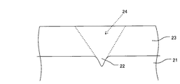
磁気ディスク用ガラス基板21の表面21a上に存在する欠陥は、図3に示すように、洗浄で容易に除去できる種類の付着物21bと、洗浄では容易に除去できない凸欠陥21cや凹欠陥21dとがある。従来の磁気ディスク用ガラス基板において、凹欠陥としてマイクロピットがある。このマイクロピットは数μmのサイズであるので、マイクロピットが存在した状態の磁気ディスク用ガラス基板上に磁性層を形成すると、そのマイクロピットに磁性層が追従して凹部となり、これがミッシングビットを構成することになる。このように、マイクロピットは、従来ミッシングビットを構成して信号的な問題を生じるために、磁気ディスク用ガラス基板にないことが望まれていた。
As shown in FIG. 3, the defects present on the
高記録密度化が進んで250GB以上/枚の記録密度になると、0.1nm近傍レベルの非常に低い表面粗さ(Ra)が必要であると共に、1μm以下のサイズの凹部欠陥、いわゆるナノピットもできるだけ少ないことが望ましいことが分った。これは、図4に示すように、ナノピット22が存在した状態の磁気ディスク用ガラス基板21上に磁性層23を形成すると、そのナノピット上の磁性層部分を起点としてクラック24が発生してしまうからである。そして、このように磁性層23にクラック24が発生すると、クラック部分から磁性層23の腐食が進行してしまう。このため、250GB以上/枚の記録密度の磁気ディスク用の基板においては、ナノピットフリーであることが磁性層の信頼性の観点から重要である。したがって、本実施の形態において対象としている欠陥は、平面視で0.1μm以上0.6μm以下のサイズで0.5nm以上2nm以下の深さの凹欠陥(いわゆるナノピット)であり、本実施の形態の技術的思想は、磁気ディスク用ガラス基板において、このナノピットの数を少なくするように制御することである。本実施の形態における欠陥数は、このような平面視で0.1μm以上0.6μm以下のサイズで0.5nm以上2nm以下の深さの欠陥を検出できる装置で検出された欠陥の数である。
If the recording density is increased to a recording density of 250 GB or more / sheet, a very low surface roughness (Ra) near the level of 0.1 nm is required, and concave defects having a size of 1 μm or less, so-called nanopits, are possible as much as possible. I found it less desirable. This is because, as shown in FIG. 4, when the
磁気ディスク用ガラス基板の表面の欠陥を検査する装置としては、例えば、図5に示す構成の装置がある。図5に示す装置は、光学式の欠陥検査装置であり、レーザドップラー法を用いた装置である。この装置においては、レーザ31と、レーザ光の反射光を検出する検出器32とを備えている。レーザ31は、測定対象物である磁気ディスク用ガラス基板21にレーザ光を照射すると共に掃引する。そして、検出器32は、レーザ光を磁気ディスク用ガラス基板21に照射しながら掃引した際の入射光と反射光との間の波長のずれからナノピットを検出する。
As an apparatus for inspecting defects on the surface of a magnetic disk glass substrate, for example, there is an apparatus having a configuration shown in FIG. The apparatus shown in FIG. 5 is an optical defect inspection apparatus, which uses a laser Doppler method. This apparatus includes a
本実施の形態に係る磁気ディスク用ガラス基板は、図5に示すような装置を用いて、波長632nmのヘリウムネオンレーザを磁気ディスク用ガラス基板に照射しながら掃引した際の入射光と反射光との間の波長のずれを用いて検出された、平面視で0.1μm以上0.6μm以下のサイズで0.5nm以上2nm以下の深さの欠陥が24cm2当たり10個未満である。このような算術平均粗さ(Ra)が0.1nm近傍のレベルにおいて、表面に存在する欠陥数が非常に少ないガラス基板は、高記録密度の磁気ディスク用の基板として好適である。 The glass substrate for a magnetic disk according to the present embodiment uses incident light and reflected light when swept while irradiating the glass substrate for magnetic disk with a helium neon laser having a wavelength of 632 nm using an apparatus as shown in FIG. The number of defects having a size of 0.1 μm or more and 0.6 μm or less in a plan view and a depth of 0.5 nm or more and 2 nm or less detected in a plan view is less than 10 per 24 cm 2 . At such a level of arithmetic average roughness (Ra) near 0.1 nm, a glass substrate with a very small number of defects present on the surface is suitable as a substrate for a high recording density magnetic disk.
また、本実施の形態に係る磁気ディスク用ガラス基板21は、主表面における最大谷深さ(Rv)に対する算術平均粗さ(Ra)の比(Ra/Rv)が0.15以上であることがより好ましい。上記構成とすることにより、このガラス基板を用いて磁気ディスクを製造した、ハードディスクドライブとしたときに、磁気ヘッド(特にDFHヘッド)の浮上安定性をより一層安定にすることができるので、高記録密度化されたハードディスクドライブであっても、上記磁気ディスク用ガラス基板を好適に適用することができる。
Further, the magnetic
また、本実施の形態にかかる磁気ディスク用ガラス基板21は、中央に穴部を有する円盤形状であり、中心から最外周までの距離を100%としたときの中心から80%以上90%以下の範囲内の主表面における算術平均粗さ(RaO)と、10%以上20%以下の範囲内の主表面における算術平均粗さ(RaI)との差(RaO−RaI)が0.01nm以下である構成とすることがより好ましい。このような構成とすることで、ガラス基板面内での表面粗さのばらつきを少なくすることができるので、磁気ヘッド(特に、DFHヘッド)の浮上安定性をより一層安定にすることができる。
Moreover, the
なお、この磁気ディスク用ガラス基板を製造する方法の一例としては、最終研磨(ここでは第2研磨工程)を基板表面に対して均等に力をかけて研磨する方法で研磨すればよい。具体的には、例えば、遊星歯車方式の研磨装置を用いて、複数のガラス基板を上下定盤で挟み研磨することで実現できる。 As an example of a method for manufacturing the glass substrate for a magnetic disk, the final polishing (here, the second polishing step) may be polished by a method in which a force is applied evenly to the substrate surface. Specifically, for example, it can be realized by sandwiching and polishing a plurality of glass substrates with upper and lower surface plates using a planetary gear type polishing apparatus.
また、本実施の形態にかかる磁気ディスク用ガラス基板21は、主表面と端面とを有しており、前記主表面と端面とには、圧縮応力層が形成されており、前記主表面の圧縮応力層深さが端面の圧縮応力層深さよりも浅い構成であってもよい。上記構成の磁気ディスク用ガラス基板を製造するためには、例えば、ガラス基板に対してイオン交換である化学強化処理を行った後で、ガラス基板の両主表面に対して研磨工程を行うことで実現できる。
Further, the magnetic
磁気ディスク用ガラス基板21の材料としては、アルミノシリケートガラス、アルミノボロシリケートガラス、ソーダライムガラスなどの多成分系ガラスや、結晶化ガラス等が挙げられる。特に、加工の容易さと、化学強化処理等を施し剛性を高めることができるという観点からアルミノシリケートガラスが好ましい。
Examples of the material of the magnetic
上記構成を有する磁気ディスク用ガラス基板上に、少なくとも磁性層を形成することにより磁気ディスクが構成されている。すなわち、磁気ディスクは、通常、磁気ディスク用ガラス基板上に、下地層、磁性層、保護層、潤滑層を順次積層することにより製造される。なお、磁気ディスクにおける下地層は、磁性層に応じて、適宜選択される。 A magnetic disk is formed by forming at least a magnetic layer on a glass substrate for a magnetic disk having the above configuration. That is, a magnetic disk is usually manufactured by sequentially laminating an underlayer, a magnetic layer, a protective layer, and a lubricating layer on a magnetic disk glass substrate. The underlayer in the magnetic disk is appropriately selected according to the magnetic layer.
また、本発明の磁気ディスクは、特定の欠陥が存在しないことから、特に、少なくとも隣接する記録トラックが磁気的に分離されたパターンド媒体として好適に用いることができる。 Further, since the magnetic disk of the present invention does not have a specific defect, it can be suitably used as a patterned medium in which at least adjacent recording tracks are magnetically separated.
(実施の形態3)
本実施の形態では、磁気ディスク用ガラス基板の製造方法について説明する。
(Embodiment 3)
In this embodiment, a method for manufacturing a magnetic disk glass substrate will be described.
本実施の形態に係る磁気ディスク用ガラス基板の製造方法においては、一対の主表面を有するガラス基板に対して少なくとも形状加工及びラッピング加工を行う工程と、前記主表面に研磨を行う研磨工程と、前記研磨後に前記ガラス基板を洗浄する洗浄工程と、を具備し、前記研磨工程において使用する研磨液に含まれる添加剤を前記洗浄工程において使用する洗浄液に含める。 In the method for manufacturing a glass substrate for a magnetic disk according to the present embodiment, a step of performing at least shape processing and lapping processing on a glass substrate having a pair of main surfaces, a polishing step of polishing the main surface, A cleaning step of cleaning the glass substrate after the polishing, and an additive contained in the polishing liquid used in the polishing step is included in the cleaning liquid used in the cleaning step.
より具体的には、磁気ディスク用ガラス基板の製造においては、(1)形状加工工程及び第1ラッピング工程、(2)端部形状工程(穴部を形成するコアリング工程、端部(外周端部及び内周端部)に面取り面を形成するチャンファリング工程(面取り面形成工程))、(3)端面研磨工程(外周端部及び内周端部)、(4)第2ラッピング工程、(5)主表面研磨工程(第1及び第2研磨工程)及び洗浄工程を備えている。また、化学強化工程を行うことが好ましい。なお、各工程は適宜順序を入れ替えることも可能であるが、本発明の磁気ディスク用ガラス基板を作製するためには、第1研磨工程後に化学強化工程を行い、第2研磨工程を行うことが好ましい。 More specifically, in manufacturing a glass substrate for a magnetic disk, (1) a shape processing step and a first lapping step, (2) an end shape step (a coring step for forming a hole, an end portion (outer peripheral end) Chamfering step (chamfering surface forming step)), (3) end surface polishing step (outer peripheral end portion and inner peripheral end portion), (4) second lapping step, 5) A main surface polishing step (first and second polishing steps) and a cleaning step are provided. Moreover, it is preferable to perform a chemical strengthening process. In addition, although it is possible to change the order of each process as appropriate, in order to produce the glass substrate for a magnetic disk of the present invention, a chemical strengthening process is performed after the first polishing process, and a second polishing process is performed. preferable.
本実施の形態においては、上記工程のうち(5)主表面研磨工程の研磨工程及び洗浄工程に着目している。この研磨工程及び洗浄工程において、使用する研磨液に含まれる添加剤を洗浄液に含めることにより、研磨剤の二次凝集の形態を保ったまま、ガラス基板表面との相互作用を維持した状態でガラス基板表面から異物を除去することができる。さらに、上記構成とすることにより、化学的親和性を高めることによって、異物を容易に除去することができる。これにより、算術平均粗さ(Ra)が0.1nm近傍のレベルにおいて表面に存在する欠陥数が非常に少ない、高記録密度磁気ディスク用の基板に好適な磁気ディスク用ガラス基板を実現することができる。 In the present embodiment, attention is paid to the polishing step and the cleaning step of (5) main surface polishing step among the above steps. In this polishing step and cleaning step, the glass contained in the state of maintaining the interaction with the glass substrate surface while maintaining the form of secondary aggregation of the polishing agent by including the additive contained in the polishing solution used in the cleaning solution. Foreign matter can be removed from the substrate surface. Furthermore, with the above configuration, foreign substances can be easily removed by increasing chemical affinity. As a result, it is possible to realize a glass substrate for a magnetic disk suitable for a substrate for a high recording density magnetic disk in which the number of defects existing on the surface is extremely small at an arithmetic mean roughness (Ra) level of about 0.1 nm. it can.
研磨工程で使用される研磨液や洗浄工程で使用される洗浄液に含める添加剤としては、酢酸、リンゴ酸、シュウ酸、マロン酸、コハク酸、グリコール酸、クエン酸、酒石酸等のカルボン酸類や、エチレンジアミン、ジエチレントリアミン等の多価アミン類、グリシン、アラニン、セリン、アスパラギン酸等のアミノ酸類や、エチレンジアミンテトラ酢酸、ニトリロトリ酢酸等のアミノポリカルボン酸類や、ヒドロキシエチレデンジホスホン酸、メチレンホスホン酸、ヒドロキシエタンホスホン酸(HEDP)等のホスホン酸類や、ホスフィン酸類や、ピロリン酸、トリポリリン酸等のリン酸類や、ピロリン酸類や、トリポリリン酸類や、アミノトリメチレンホスホン酸類等が挙げられる。また、上記例示の塩を用いてもよい。このうち、リン酸ナトリウム、リン酸2水素1ナトリウム、リン酸1水素2ナトリウム、シュウ酸カリウム等の多価酸の塩であることがより好ましい。 Additives included in the polishing liquid used in the polishing process and the cleaning liquid used in the cleaning process include carboxylic acids such as acetic acid, malic acid, oxalic acid, malonic acid, succinic acid, glycolic acid, citric acid, tartaric acid, Polyvalent amines such as ethylenediamine and diethylenetriamine, amino acids such as glycine, alanine, serine and aspartic acid, aminopolycarboxylic acids such as ethylenediaminetetraacetic acid and nitrilotriacetic acid, hydroxyethylidene diphosphonic acid, methylenephosphonic acid, hydroxyethane Examples thereof include phosphonic acids such as phosphonic acid (HEDP), phosphinic acids, phosphoric acids such as pyrophosphoric acid and tripolyphosphoric acid, pyrophosphoric acids, tripolyphosphoric acids, and aminotrimethylene phosphonic acids. Moreover, you may use the salt of the said illustration. Of these, salts of polyvalent acids such as sodium phosphate, monosodium dihydrogen phosphate, disodium monohydrogen phosphate, and potassium oxalate are more preferable.
このうち、キレート作用を生じさせるもの(キレート剤)としては、例えば、シュウ酸・マロン酸・グリコール酸・クエン酸・酒石酸等のカルボン酸類や、エチレンジアミン・ジエチレントリアミン等の多価アミン、グリシン・アラニン・セリン・アスパラギン酸等のアミノ酸、エチレンジアミンテトラ酢酸・ニトリロトリ酢酸等のアミノポリカルボン酸類、ヒドロキシエチレデンジホスホン酸・メチレンホスホン酸等のホスホン酸類、ピロリン酸・トリポリリン酸等のリン酸類等が挙げられる。また、分散作用を生じさせるもの(分散剤)としては、例えば、スルホ脂肪酸エステル、アルキルベンゼンスルホン酸、アルキル硫酸塩、アルキル硫酸トリエターノールアミン、アルキルエーテル硫酸エステル等の陰イオン性界面活性剤、脂肪酸ジエタノールアミド、ポリオキシエチレンアルキルエーテル、ポリオキシエチレンアルキルフェニルエーテル等の非イオン性界面活性剤、アミン等を挙げることができる。 Among them, examples of chelating agents (chelating agents) include carboxylic acids such as oxalic acid, malonic acid, glycolic acid, citric acid, and tartaric acid, polyvalent amines such as ethylenediamine and diethylenetriamine, glycine, alanine, Examples thereof include amino acids such as serine and aspartic acid, aminopolycarboxylic acids such as ethylenediaminetetraacetic acid and nitrilotriacetic acid, phosphonic acids such as hydroxyethylene diphosphonic acid and methylenephosphonic acid, and phosphoric acids such as pyrophosphoric acid and tripolyphosphoric acid. Examples of those that cause a dispersing action (dispersing agents) include anionic surfactants such as sulfo fatty acid esters, alkylbenzene sulfonic acids, alkyl sulfates, alkyl sulfate triethanolamines, alkyl ether sulfates, and fatty acids. Nonionic surfactants such as diethanolamide, polyoxyethylene alkyl ether and polyoxyethylene alkyl phenyl ether, amines and the like can be mentioned.
また、添加剤は、ガラス基板の表面粗さの抑制及び異物の除去能力や研磨剤の過剰凝集や凝集不足、及び洗浄液排水処理時の環境への影響などを考慮して、研磨液中に0.01重量%以上、10.0重量%以下の範囲内、より好ましくは0.1重量%以上、5.0重量%以下の範囲内で含有されていることが好ましく、洗浄液中に0.01重量%以上、5.0重量%以下、より好ましくは0.1重量%以上、3.0重量%以下の範囲内で含有されていることが好ましい。 In addition, the additive is not contained in the polishing liquid in consideration of the suppression of the surface roughness of the glass substrate, the ability to remove foreign substances, the excessive aggregation or insufficient aggregation of the abrasive, and the environmental impact during the cleaning liquid drainage treatment. 0.01 wt% or more and 10.0 wt% or less, more preferably 0.1 wt% or more and 5.0 wt% or less. It is preferably contained in the range of not less than 5.0% by weight and not more than 5.0% by weight, more preferably not less than 0.1% by weight and not more than 3.0% by weight.
次に、本発明の効果を明確にするために行った実施例について説明する。 Next, examples performed for clarifying the effects of the present invention will be described.
(実施の形態1に係る実施例1)
以下に、本発明を適用した磁気ディスク用ガラス基板及び磁気ディスクの製造方法について実施例を説明する。この磁気ディスク用ガラス基板及び磁気ディスクは、3.5インチ型ディスク(φ89mm)、2.5インチ型ディスク(φ65mm)などの所定の形状を有する磁気ディスクとして製造される。
(Example 1 according to Embodiment 1)
Examples of a glass substrate for a magnetic disk and a method for manufacturing the magnetic disk to which the present invention is applied will be described below. The magnetic disk glass substrate and the magnetic disk are manufactured as magnetic disks having a predetermined shape such as a 3.5-inch disk (φ89 mm) and a 2.5-inch disk (φ65 mm).
(1)第1ラッピング工程
本実施例に係る磁気ディスク用ガラス基板の製造方法においては、まず、板状ガラスの表面をラッピング(研削)加工してガラス母材とし、このガラス母材を切断してガラスディスクを切り出す。板状ガラスとしては、様々な板状ガラスを用いることができる。この板状ガラスは、例えば、溶融ガラスを材料として、プレス法やフロート法、ダウンドロー法、リドロー法、フュージョン法など、公知の製造方法を用いて製造することができる。これらのうち、プレス法を用いれば、板状ガラスを廉価に製造することができる。板状ガラスの材質としては、アモルファスガラスやガラスセラミクス(結晶化ガラス)を利用できる。板状ガラスの材料としては、アルミノシリケートガラス、ソーダライムガラス、ボロシリケートガラス等を用いることができる。特にアモルファスガラスとしては、化学強化を施すことができ、また主表面の平坦性及び基板強度において優れた磁気ディスク用ガラス基板を供給することができるという点で、アルミノシリケートガラスを好ましく用いることができる。
(1) First Lapping Step In the method for manufacturing a glass substrate for a magnetic disk according to the present embodiment, first, the surface of the plate glass is lapped (ground) to obtain a glass base material, and this glass base material is cut. And cut out the glass disc. Various plate glasses can be used as the plate glass. This plate-like glass can be manufactured by using a known manufacturing method such as a press method, a float method, a downdraw method, a redraw method, or a fusion method using a molten glass as a material. Of these, plate glass can be produced at low cost by using the pressing method. As the material of the plate glass, amorphous glass or glass ceramics (crystallized glass) can be used. As the material for the plate glass, aluminosilicate glass, soda lime glass, borosilicate glass, or the like can be used. In particular, as an amorphous glass, an aluminosilicate glass can be preferably used in that it can be chemically strengthened and can supply a glass substrate for a magnetic disk excellent in flatness of the main surface and substrate strength. .
本実施例においては、溶融させたアルミノシリケートガラスを上型、下型、胴型を用いたダイレクトプレスによりディスク形状に成型し、アモルファスの板状ガラスを得た。なお、アルミノシリケートガラスとしては、SiO2:58重量%〜75重量%、Al2O3:5重量%〜23重量%、Li2O:3重量%〜10重量%、Na2O:4重量%〜13重量%を主成分として含有するガラスを使用した。 In this example, the melted aluminosilicate glass was molded into a disk shape by direct pressing using an upper mold, a lower mold, and a barrel mold to obtain an amorphous plate glass. As the aluminosilicate glass, SiO 2: 58 wt% to 75 wt%, Al 2 O 3: 5 wt% to 23 wt%, Li 2 O: 3% to 10% by weight, Na 2 O: 4 by weight Glass containing from 13 to 13% by weight as a main component was used.
次に、この板状ガラスの両主表面をラッピング加工し、ディスク状のガラス母材とした。このラッピング加工は、遊星歯車機構を利用した両面ラッピング装置により、アルミナ系遊離砥粒を用いて行った。具体的には、板状ガラスの両面に上下からラップ定盤を押圧させ、遊離砥粒を含む研削液を板状ガラスの主表面上に供給し、これらを相対的に移動させてラッピング加工を行った。このラッピング加工により、平坦な主表面を有するガラス母材を得た。 Next, both main surfaces of the plate glass were lapped to form a disk-shaped glass base material. This lapping process was performed using alumina free abrasive grains with a double-sided lapping apparatus using a planetary gear mechanism. Specifically, the lapping platen is pressed on both sides of the plate glass from above and below, the grinding liquid containing free abrasive grains is supplied onto the main surface of the plate glass, and these are moved relative to each other for lapping. went. By this lapping process, a glass base material having a flat main surface was obtained.
(2)形状加工工程(コアリング、チャンファリング)
次に、円筒状のダイヤモンドドリルを用いて、このガラス基板の中心部に内孔を形成し、円環状のガラス基板とした(コアリング)。そして内周端面及び外周端面をダイヤモンド砥石によって研削し、所定の面取り加工を施した(チャンファリング)。
(2) Shape processing process (coring, chamfering)
Next, using a cylindrical diamond drill, an inner hole was formed in the center of the glass substrate to obtain an annular glass substrate (coring). Then, the inner peripheral end face and the outer peripheral end face were ground with a diamond grindstone, and a predetermined chamfering process was performed (chambering).
(3)第2ラッピング工程
次に、得られたガラス基板の両主表面について、第1ラッピング工程と同様に、第2ラッピング加工を行った。この第2ラッピング工程を行うことにより、前工程である切り出し工程や端面研磨工程において主表面に形成された微細な凹凸形状を予め除去しておくことができ、後続の主表面に対する研磨工程を短時間で完了させることができるようになる。
(3) Second Lapping Step Next, a second lapping process was performed on both main surfaces of the obtained glass substrate in the same manner as in the first lapping step. By performing this second lapping step, it is possible to remove in advance the fine unevenness formed on the main surface in the cutting step and end surface polishing step, which are the previous steps, and shorten the subsequent polishing step on the main surface. Will be able to be completed in time.
(4)端面研磨工程
次に、ガラス基板の外周端面及び内周端面について、ブラシ研磨方法により、鏡面研磨を行った。このとき、研磨砥粒としては、酸化セリウム砥粒を含むスラリー(遊離砥粒)を用いた。
(4) End surface polishing step Next, the outer peripheral end surface and the inner peripheral end surface of the glass substrate were mirror-polished by a brush polishing method. At this time, as the abrasive grains, a slurry (free abrasive grains) containing cerium oxide abrasive grains was used.
そして、端面研磨工程を終えたガラス基板を水洗浄した。この端面研磨工程により、ガラス基板の端面は、ナトリウムやカリウムの析出の発生を防止できる鏡面状態に加工された。 And the glass substrate which finished the end surface grinding | polishing process was washed with water. By this end face polishing step, the end face of the glass substrate was processed into a mirror state that can prevent the precipitation of sodium and potassium.
(5)第1研磨工程
主表面研磨工程として、まず第1研磨工程を施した。この第1研磨工程は、前述のラッピング工程において主表面に残留したキズや歪みの除去を主たる目的とするものである。この第1研磨工程においては、遊星歯車機構を有する両面研磨装置により、硬質樹脂ポリッシャを用いて、主表面の研磨を行った。研磨剤としては、酸化セリウム砥粒を用いた。
(5) 1st grinding | polishing process The 1st grinding | polishing process was first given as a main surface grinding | polishing process. This first polishing step is mainly intended to remove scratches and distortions remaining on the main surface in the lapping step described above. In the first polishing step, the main surface was polished using a hard resin polisher by a double-side polishing apparatus having a planetary gear mechanism. As the abrasive, cerium oxide abrasive grains were used.
この第1研磨工程を終えたガラス基板を、中性洗剤、純水、IPA(イソプロピルアルコール)、の各洗浄槽に順次浸漬して、洗浄した。 The glass substrate which finished this 1st grinding | polishing process was immersed in each washing tank of neutral detergent, a pure water, and IPA (isopropyl alcohol) one by one, and was wash | cleaned.
(6)化学強化工程
次に、前述の端面研磨工程及び第1主表面研磨工程を終えたガラス基板に、化学強化処理(イオン交換処理)を施した。化学強化は、硝酸カリウム(60%)と硝酸ナトリウム(40%)を混合した化学強化溶液を用意し、この化学強化溶液を400℃に加熱しておくとともに、洗浄済みのガラス基板を300℃に予熱し、化学強化溶液中に約3時間浸漬することによって行った。この浸漬の際には、ガラス基板の表面全体が化学強化されるようにするため、複数のガラス基板が端面で保持されるように、ホルダに収納した状態で行った。
(6) Chemical strengthening process Next, the glass substrate which finished the above-mentioned end surface grinding | polishing process and 1st main surface grinding | polishing process was given the chemical strengthening process (ion exchange process). For chemical strengthening, a chemical strengthening solution prepared by mixing potassium nitrate (60%) and sodium nitrate (40%) is prepared, and the chemically strengthened solution is heated to 400 ° C., and the cleaned glass substrate is preheated to 300 ° C. And was immersed in the chemical strengthening solution for about 3 hours. In this immersion, in order to chemically strengthen the entire surface of the glass substrate, it was performed in a state of being housed in a holder so that a plurality of glass substrates were held at the end surfaces.
このように、化学強化溶液に浸漬処理することによって、ガラス基板の表層のリチウムイオン及びナトリウムイオンが、化学強化溶液中のナトリウムイオン及びカリウムイオンにそれぞれ置換され、ガラス基板が強化される。ガラス基板の表層に形成された圧縮応力層の厚さは、約100μm〜200μmであった。 Thus, by immersing in a chemical strengthening solution, the lithium ion and sodium ion of the surface layer of a glass substrate are each substituted by the sodium ion and potassium ion in a chemical strengthening solution, and a glass substrate is strengthened. The thickness of the compressive stress layer formed on the surface layer of the glass substrate was about 100 μm to 200 μm.
化学強化処理を終えたガラス基板を、20℃の水槽に浸漬して急冷し、約10分間維持した。そして、急冷を終えたガラス基板を、約40℃に加熱した濃硫酸に浸漬して洗浄を行った。さらに、硫酸洗浄を終えたガラス基板を純水、IPAの各洗浄槽に順次浸漬して洗浄した。 The glass substrate that had been subjected to the chemical strengthening treatment was immersed in a 20 ° C. water bath and rapidly cooled, and maintained for about 10 minutes. And the glass substrate which finished quenching was immersed in the concentrated sulfuric acid heated at about 40 degreeC, and was wash | cleaned. Further, the glass substrate that had been subjected to the sulfuric acid cleaning was sequentially immersed in each cleaning bath of pure water and IPA for cleaning.
(7)第2研磨工程
次に、主表面研磨工程として、第2研磨工程を施した。この第2研磨工程は、主表面を鏡面状に仕上げることを目的とする。この第2研磨工程においては、遊星歯車機構を有する両面研磨装置により、軟質発泡樹脂ポリッシャを用いて、主表面の鏡面研磨を行った。研磨剤としては、第1研磨工程で用いた酸化セリウム砥粒よりも微細なコロイダルシリカ砥粒(平均粒子径5nm〜80nm)を用いたスラリーを使用した。
(7) Second Polishing Step Next, a second polishing step was performed as the main surface polishing step. The purpose of this second polishing step is to finish the main surface into a mirror surface. In the second polishing step, mirror polishing of the main surface was performed using a soft foamed resin polisher by a double-side polishing apparatus having a planetary gear mechanism. As the abrasive, a slurry using colloidal silica abrasive grains (average particle diameter of 5 nm to 80 nm) finer than the cerium oxide abrasive grains used in the first polishing step was used.
そして、上記スラリーのpHを2に設定して研磨を行った。このとき、上記スラリーに酢酸及び酢酸塩を含む添加剤を加えて研磨を行っている。これは、研磨工程中にスラリーのpHを一定にコントロールするためである。上記スラリー(研磨液)としては、超純水に上記コロイド状シリカ粒子を加えた混合液を用い、添加剤としてクエン酸を0.5重量%添加したものを用いた。 Then, polishing was performed with the pH of the slurry set to 2. At this time, polishing is performed by adding an additive containing acetic acid and acetate to the slurry. This is for controlling the pH of the slurry constant during the polishing process. As the slurry (polishing liquid), a mixed liquid obtained by adding the colloidal silica particles to ultrapure water and 0.5% by weight of citric acid as an additive was used.
(8)洗浄工程
この第2研磨工程を終えたガラス基板を、酸洗浄、アルカリ洗浄純水、IPAの各洗浄槽に順次浸漬して、洗浄した。なお、各洗浄槽には、超音波を印加した。
(8) Cleaning Step The glass substrate after the second polishing step was sequentially immersed in each cleaning bath of acid cleaning, alkaline cleaning pure water, and IPA and cleaned. Note that ultrasonic waves were applied to each cleaning tank.
そして、上記酸洗浄の際に、上記第2研磨工程で添加した添加剤と同じものを酸洗浄における添加剤として加えた。具体的にはクエン酸を0.15重量%に調整した酸溶液で酸洗浄を行った。これは、スラリー中に含まれる成分と同じものを洗浄液に入れることで基板上に固着したスラリーを効率的に除去するためである。これにより、ガラス基板に固着するパーティクルを低減させることができる。 And the same thing as the additive added at the said 2nd grinding | polishing process was added as an additive in acid cleaning in the said acid cleaning. Specifically, acid cleaning was performed with an acid solution in which citric acid was adjusted to 0.15% by weight. This is for efficiently removing the slurry fixed on the substrate by putting the same components contained in the slurry into the cleaning liquid. Thereby, the particles adhering to the glass substrate can be reduced.
上記の如く、第1ラッピング工程、切り出し工程、第2ラッピング工程、端面研磨工程、第1研磨工程、化学強化工程及び第2研磨工程を施すことにより、平坦、かつ、平滑な、高剛性の磁気ディスク用ガラス基板を得た。 As described above, by applying the first lapping step, the cutting step, the second lapping step, the end surface polishing step, the first polishing step, the chemical strengthening step, and the second polishing step, a flat, smooth, and highly rigid magnetic A glass substrate for disk was obtained.
(実施の形態1に係る比較例1)
研磨工程において使用する研磨液に含まれる添加剤を洗浄工程において使用する洗浄液に含めなかったこと以外は、実施例1と同様にしてガラス基板を作製した。
(Comparative Example 1 according to Embodiment 1)
A glass substrate was produced in the same manner as in Example 1 except that the additive contained in the polishing liquid used in the polishing process was not included in the cleaning liquid used in the cleaning process.
(実施の形態1に係る比較例2)
洗浄工程において使用する洗浄液中のクエン酸の含有量を0.005重量%に調整したこと以外は、実施例1と同様にしてガラス基板を作製した。
(Comparative Example 2 according to Embodiment 1)
A glass substrate was produced in the same manner as in Example 1 except that the content of citric acid in the cleaning liquid used in the cleaning process was adjusted to 0.005% by weight.
(欠陥検査1)
実施例、比較例で得られたそれぞれのガラス基板について、図2に示す光学式欠陥検査装置(KLA−Tencor社製、商品名:OSA6100)で欠陥を検査した。このとき、測定条件としては、レーザパワ25mWのレーザ波長405nm、レーザスポット径5μmとし、ガラス基板の中心から15mm〜31.5mmの間の領域を測定した。0.1μm以上0.3μm以下のサイズとして検出された欠陥のうち、固着している欠陥の個数(24cm2当たり)を表1に示す。
(Defect inspection 1)
About each glass substrate obtained by the Example and the comparative example, the defect was test | inspected with the optical defect inspection apparatus (KLA-Tencor company make, brand name: OSA6100) shown in FIG. At this time, the measurement conditions were a laser wavelength of 405 nm with a laser power of 25 mW and a laser spot diameter of 5 μm, and a region between 15 mm and 31.5 mm from the center of the glass substrate was measured. Table 1 shows the number of fixed defects (per 24 cm 2 ) among defects detected as a size of 0.1 μm or more and 0.3 μm or less.
(ガラス基板の表面測定)
実施例、比較例で得られたそれぞれのガラス基板について、原子間力顕微鏡を用いて2μm×2μm角で256×256ピクセルの解像度で測定して表面粗さ(算術平均粗さ(Ra))を求めた。結果を表1に示す。
(Measurement of glass substrate surface)
The surface roughness (arithmetic average roughness (Ra)) of each glass substrate obtained in Examples and Comparative Examples was measured with an atomic force microscope at a resolution of 256 × 256 pixels at 2 μm × 2 μm square. Asked. The results are shown in Table 1.
また、ガラス基板の中心から最外周までの距離を100%としたときの中心から80%以上90%以下の範囲内の主表面における算術平均粗さ(RaO)と10%以上20%以下の範囲内の主表面における算術平均粗さ(RaI)を測定し、両者の差(RaO−RaI)を求めた。結果を表1に示す。 Further, the arithmetic average roughness (Ra 2 O 3 ) on the main surface within the range of 80% to 90% from the center when the distance from the center of the glass substrate to the outermost periphery is 100% and 10% to 20% The arithmetic average roughness (Ra I ) on the main surface within the range was measured, and the difference between the two (Ra O -Ra I ) was determined. The results are shown in Table 1.
ガラス基板の表面における最大山高さ(Rp)及び算術平均粗さ(Ra)を測定し、最大山高さ(Rp)に対する算術平均粗さ(Ra)の比(Ra/Rp)を求めた。結果を表1に示す。 The maximum peak height (Rp) and arithmetic average roughness (Ra) on the surface of the glass substrate were measured, and the ratio (Ra / Rp) of the arithmetic average roughness (Ra) to the maximum peak height (Rp) was determined. The results are shown in Table 1.
次に、実施例及び比較例で得られたそれぞれのガラス基板上に、付着層、軟磁性層、前下地層、下地層、非磁性グラニュラ層、第1磁気記録層、第2磁気記録層、補助記録層、保護層及び潤滑層を順次積層して磁気ディスクを作製した。 Next, on each glass substrate obtained in Examples and Comparative Examples, an adhesion layer, a soft magnetic layer, a pre-underlayer, an underlayer, a nonmagnetic granular layer, a first magnetic recording layer, a second magnetic recording layer, An auxiliary recording layer, a protective layer, and a lubricating layer were sequentially laminated to produce a magnetic disk.
具体的には、ディスク基体上に、真空引きを行った成膜装置を用いて、DCマグネトロンスパッタリング法にてAr雰囲気中で、付着層から補助記録層まで順次成膜を行った。付着層は、CrTiとした。軟磁性層は、FeCoTaZrからなる第1軟磁性層及び第2軟磁性層の間にRuスペーサ層が介在しているものとした。前下地層の組成はfcc構造のNiW合金とした。下地層は、低圧Ar下でされた第1下地層(Ru)上に、高圧Ar下で成膜した第2下地層(Ru)とした。非磁性グラニュラ層の組成は非磁性のCoCr−SiO2とした。第1磁気記録層の組成は、CoCrPt−Cr2O3とし、第2磁気記録層の組成は、CoCrPt−SiO2−TiO2とした。補助記録層の組成はCoCrPtBとした。媒体保護層はCVD法によりC2H4を用いて成膜し、同一チャンバ内で、表面に窒素を導入する窒化処理を行うことにより形成した。潤滑層はディップコート法によりPFPEを用いて形成した。 Specifically, film formation was sequentially performed on the disk substrate from the adhesion layer to the auxiliary recording layer in an Ar atmosphere by a DC magnetron sputtering method using a vacuum film forming apparatus. The adhesion layer was CrTi. In the soft magnetic layer, a Ru spacer layer is interposed between the first soft magnetic layer and the second soft magnetic layer made of FeCoTaZr. The composition of the pre-underlayer was a NiW alloy having an fcc structure. The underlayer was a second underlayer (Ru) formed under high-pressure Ar on the first underlayer (Ru) under low-pressure Ar. The composition of the nonmagnetic granular layer was nonmagnetic CoCr—SiO 2 . The composition of the first magnetic recording layer was CoCrPt—Cr 2 O 3, and the composition of the second magnetic recording layer was CoCrPt—SiO 2 —TiO 2 . The composition of the auxiliary recording layer was CoCrPtB. The medium protective layer was formed using C 2 H 4 by a CVD method, and was formed by performing a nitriding treatment in which nitrogen was introduced into the surface in the same chamber. The lubricating layer was formed using PFPE by a dip coating method.
このとき、ガラス基板の主表面上の欠陥量(コンタミ量)が非常に低いレベルであったので、スパッタリングによる磁性粒子の配向が揃い、高密度記憶が可能な磁性層の形成が可能であった。この得られた磁気ディスクについて、耐久性試験を行った。 At this time, since the amount of defects (contamination amount) on the main surface of the glass substrate was at a very low level, the magnetic particles were aligned by sputtering, and a magnetic layer capable of high-density memory could be formed. . The obtained magnetic disk was subjected to a durability test.
(耐久性試験)
耐久性試験は、磁気ディスクをLUL(ロード・アンロード)方式のHDD装置に搭載して行った。具体的には、磁気記録装置に、上記磁気ディスクと、巨大磁気抵抗効果型再生素子(GMR素子)を備えたDFHヘッドとを装着し、ヘッド浮上量を6nmでロード・アンロード試験を規定回数(200万回)実施することにより耐久性試験を行った。結果を表1に示す。
(Durability test)
The durability test was performed by mounting a magnetic disk on a LUL (load / unload) type HDD device. Specifically, the above magnetic disk and a DFH head equipped with a giant magnetoresistive reproducing element (GMR element) are mounted on the magnetic recording apparatus, and the load / unload test is performed a specified number of times with a head flying height of 6 nm. The durability test was performed by carrying out (2 million times). The results are shown in Table 1.

(実施の形態2に係る実施例1)
以下に、本発明を適用した磁気ディスク用ガラス基板及び磁気ディスクの製造方法について実施例を説明する。この磁気ディスク用ガラス基板及び磁気ディスクは、3.5インチ型ディスク(φ89mm)、2.5インチ型ディスク(φ65mm)などの所定の形状を有する磁気ディスクとして製造される。
(Example 1 according to Embodiment 2)
Examples of a glass substrate for a magnetic disk and a method for manufacturing the magnetic disk to which the present invention is applied will be described below. The magnetic disk glass substrate and the magnetic disk are manufactured as magnetic disks having a predetermined shape such as a 3.5-inch disk (φ89 mm) and a 2.5-inch disk (φ65 mm).
(1)第1ラッピング工程
本実施例に係る磁気ディスク用ガラス基板の製造方法においては、まず、板状ガラスの表面をラッピング(研削)加工してガラス母材とし、このガラス母材を切断してガラスディスクを切り出す。板状ガラスとしては、様々な板状ガラスを用いることができる。この板状ガラスは、例えば、溶融ガラスを材料として、プレス法やフロート法、ダウンドロー法、リドロー法、フュージョン法など、公知の製造方法を用いて製造することができる。これらのうち、プレス法を用いれば、板状ガラスを廉価に製造することができる。板状ガラスの材質としては、アモルファスガラスやガラスセラミクス(結晶化ガラス)を利用できる。板状ガラスの材料としては、アルミノシリケートガラス、ソーダライムガラス、ボロシリケートガラス等を用いることができる。特にアモルファスガラスとしては、化学強化を施すことができ、また主表面の平坦性及び基板強度において優れた磁気ディスク用ガラス基板を供給することができるという点で、アルミノシリケートガラスを好ましく用いることができる。
(1) First Lapping Step In the method for manufacturing a glass substrate for a magnetic disk according to the present embodiment, first, the surface of the plate glass is lapped (ground) to obtain a glass base material, and this glass base material is cut. And cut out the glass disc. Various plate glasses can be used as the plate glass. This plate-like glass can be manufactured by using a known manufacturing method such as a press method, a float method, a downdraw method, a redraw method, or a fusion method using a molten glass as a material. Of these, plate glass can be produced at low cost by using the pressing method. As the material of the plate glass, amorphous glass or glass ceramics (crystallized glass) can be used. As the material for the plate glass, aluminosilicate glass, soda lime glass, borosilicate glass, or the like can be used. In particular, as an amorphous glass, an aluminosilicate glass can be preferably used in that it can be chemically strengthened and can supply a glass substrate for a magnetic disk excellent in flatness of the main surface and substrate strength. .
本実施例においては、溶融させたアルミノシリケートガラスを上型、下型、胴型を用いたダイレクトプレスによりディスク形状に成型し、アモルファスの板状ガラスを得た。なお、アルミノシリケートガラスとしては、SiO2:58重量%〜75重量%、Al2O3:5重量%〜23重量%、Li2O:3重量%〜10重量%、Na2O:4重量%〜13重量%を主成分として含有するガラスを使用した。 In this example, the melted aluminosilicate glass was molded into a disk shape by direct pressing using an upper mold, a lower mold, and a barrel mold to obtain an amorphous plate glass. As the aluminosilicate glass, SiO 2: 58 wt% to 75 wt%, Al 2 O 3: 5 wt% to 23 wt%, Li 2 O: 3% to 10% by weight, Na 2 O: 4 by weight Glass containing from 13 to 13% by weight as a main component was used.
次に、この板状ガラスの両主表面をラッピング加工し、ディスク状のガラス母材とした。このラッピング加工は、遊星歯車機構を利用した両面ラッピング装置により、アルミナ系遊離砥粒を用いて行った。具体的には、板状ガラスの両面に上下からラップ定盤を押圧させ、遊離砥粒を含む研削液を板状ガラスの主表面上に供給し、これらを相対的に移動させてラッピング加工を行った。このラッピング加工により、平坦な主表面を有するガラス母材を得た。 Next, both main surfaces of the plate glass were lapped to form a disk-shaped glass base material. This lapping process was performed using alumina free abrasive grains with a double-sided lapping apparatus using a planetary gear mechanism. Specifically, the lapping platen is pressed on both sides of the plate glass from above and below, the grinding liquid containing free abrasive grains is supplied onto the main surface of the plate glass, and these are moved relative to each other for lapping. went. By this lapping process, a glass base material having a flat main surface was obtained.
(2)形状加工工程(コアリング、チャンファリング)
次に、円筒状のダイヤモンドドリルを用いて、このガラス基板の中心部に内孔を形成し、円環状のガラス基板とした(コアリング)。そして内周端面及び外周端面をダイヤモンド砥石によって研削し、所定の面取り加工を施した(チャンファリング)。
(2) Shape processing process (coring, chamfering)
Next, using a cylindrical diamond drill, an inner hole was formed in the center of the glass substrate to obtain an annular glass substrate (coring). Then, the inner peripheral end face and the outer peripheral end face were ground with a diamond grindstone, and a predetermined chamfering process was performed (chambering).
(3)第2ラッピング工程
次に、得られたガラス基板の両主表面について、第1ラッピング工程と同様に、第2ラッピング加工を行った。この第2ラッピング工程を行うことにより、前工程である切り出し工程や端面研磨工程において主表面に形成された微細な凹凸形状を予め除去しておくことができ、後続の主表面に対する研磨工程を短時間で完了させることができるようになる。
(3) Second Lapping Step Next, a second lapping process was performed on both main surfaces of the obtained glass substrate in the same manner as in the first lapping step. By performing this second lapping step, it is possible to remove in advance the fine unevenness formed on the main surface in the cutting step and end surface polishing step, which are the previous steps, and shorten the subsequent polishing step on the main surface. Will be able to be completed in time.
(4)端面研磨工程
次に、ガラス基板の外周端面及び内周端面について、ブラシ研磨方法により、鏡面研磨を行った。このとき、研磨砥粒としては、酸化セリウム砥粒を含むスラリー(遊離砥粒)を用いた。
(4) End surface polishing step Next, the outer peripheral end surface and the inner peripheral end surface of the glass substrate were mirror-polished by a brush polishing method. At this time, as the abrasive grains, a slurry (free abrasive grains) containing cerium oxide abrasive grains was used.
そして、端面研磨工程を終えたガラス基板を水洗浄した。この端面研磨工程により、ガラス基板の端面は、ナトリウムやカリウムの析出の発生を防止できる鏡面状態に加工された。 And the glass substrate which finished the end surface grinding | polishing process was washed with water. By this end face polishing step, the end face of the glass substrate was processed into a mirror state that can prevent the precipitation of sodium and potassium.
(5)第1研磨工程
主表面研磨工程として、まず第1研磨工程を施した。この第1研磨工程は、前述のラッピング工程において主表面に残留したキズや歪みの除去を主たる目的とするものである。この第1研磨工程においては、遊星歯車機構を有する両面研磨装置により、硬質樹脂ポリッシャを用いて、主表面の研磨を行った。研磨剤としては、酸化セリウム砥粒を用いた。
(5) 1st grinding | polishing process The 1st grinding | polishing process was first given as a main surface grinding | polishing process. This first polishing step is mainly intended to remove scratches and distortions remaining on the main surface in the lapping step described above. In the first polishing step, the main surface was polished using a hard resin polisher by a double-side polishing apparatus having a planetary gear mechanism. As the abrasive, cerium oxide abrasive grains were used.
この第1研磨工程を終えたガラス基板を、中性洗剤、純水、IPA(イソプロピルアルコール)、の各洗浄槽に順次浸漬して、洗浄した。 The glass substrate which finished this 1st grinding | polishing process was immersed in each washing tank of neutral detergent, a pure water, and IPA (isopropyl alcohol) one by one, and was wash | cleaned.
(6)化学強化工程
次に、前述の端面研磨工程及び第1主表面研磨工程を終えたガラス基板に、化学強化処理(イオン交換処理)を施した。化学強化は、硝酸カリウム(60%)と硝酸ナトリウム(40%)を混合した化学強化溶液を用意し、この化学強化溶液を400℃に加熱しておくとともに、洗浄済みのガラス基板を300℃に予熱し、化学強化溶液中に約3時間浸漬することによって行った。この浸漬の際には、ガラス基板の表面全体が化学強化されるようにするため、複数のガラス基板が端面で保持されるように、ホルダに収納した状態で行った。
(6) Chemical strengthening process Next, the glass substrate which finished the above-mentioned end surface grinding | polishing process and 1st main surface grinding | polishing process was given the chemical strengthening process (ion exchange process). For chemical strengthening, a chemical strengthening solution prepared by mixing potassium nitrate (60%) and sodium nitrate (40%) is prepared, and the chemically strengthened solution is heated to 400 ° C., and the cleaned glass substrate is preheated to 300 ° C. And was immersed in the chemical strengthening solution for about 3 hours. In this immersion, in order to chemically strengthen the entire surface of the glass substrate, it was performed in a state of being housed in a holder so that a plurality of glass substrates were held at the end surfaces.
このように、化学強化溶液に浸漬処理することによって、ガラス基板の表層のリチウムイオン及びナトリウムイオンが、化学強化溶液中のナトリウムイオン及びカリウムイオンにそれぞれ置換され、ガラス基板が強化される。ガラス基板の表層に形成された圧縮応力層の厚さは、約100μm〜200μmであった。 Thus, by immersing in a chemical strengthening solution, the lithium ion and sodium ion of the surface layer of a glass substrate are each substituted by the sodium ion and potassium ion in a chemical strengthening solution, and a glass substrate is strengthened. The thickness of the compressive stress layer formed on the surface layer of the glass substrate was about 100 μm to 200 μm.
化学強化処理を終えたガラス基板を、20℃の水槽に浸漬して急冷し、約10分間維持した。そして、急冷を終えたガラス基板を、約40℃に加熱した濃硫酸に浸漬して洗浄を行った。さらに、硫酸洗浄を終えたガラス基板を純水、IPAの各洗浄槽に順次浸漬して洗浄した。 The glass substrate that had been subjected to the chemical strengthening treatment was immersed in a 20 ° C. water bath and rapidly cooled, and maintained for about 10 minutes. And the glass substrate which finished quenching was immersed in the concentrated sulfuric acid heated at about 40 degreeC, and was wash | cleaned. Further, the glass substrate that had been subjected to the sulfuric acid cleaning was sequentially immersed in each cleaning bath of pure water and IPA for cleaning.
(7)第2研磨工程
次に、主表面研磨工程として、第2研磨工程を施した。この第2研磨工程は、主表面を鏡面状に仕上げることを目的とする。この第2研磨工程においては、遊星歯車機構を有する両面研磨装置により、軟質発泡樹脂ポリッシャを用いて、主表面の鏡面研磨を行った。研磨剤としては、第1研磨工程で用いた酸化セリウム砥粒よりも微細なコロイダルシリカ砥粒(平均粒子径5nm〜80nm)を用いたスラリーを使用した。
(7) Second Polishing Step Next, a second polishing step was performed as the main surface polishing step. The purpose of this second polishing step is to finish the main surface into a mirror surface. In the second polishing step, mirror polishing of the main surface was performed using a soft foamed resin polisher by a double-side polishing apparatus having a planetary gear mechanism. As the abrasive, a slurry using colloidal silica abrasive grains (average particle diameter of 5 nm to 80 nm) finer than the cerium oxide abrasive grains used in the first polishing step was used.
そして、上記スラリーのpHを2に設定して研磨を行った。このとき、上記スラリーに酢酸及び酢酸塩を含む添加剤を加えて研磨を行っている。これは、研磨工程中にスラリーのpHを一定にコントロールするためである。上記スラリー(研磨液)としては、超純水に上記コロイド状シリカ粒子を加えた混合液を用い、添加剤としてクエン酸を0.5重量%添加したものを用いた。 Then, polishing was performed with the pH of the slurry set to 2. At this time, polishing is performed by adding an additive containing acetic acid and acetate to the slurry. This is for controlling the pH of the slurry constant during the polishing process. As the slurry (polishing liquid), a mixed liquid obtained by adding the colloidal silica particles to ultrapure water and 0.5% by weight of citric acid as an additive was used.
(8)洗浄工程
この第2研磨工程を終えたガラス基板を、酸洗浄、アルカリ洗浄純水、IPAの各洗浄槽に順次浸漬して、洗浄した。なお、各洗浄槽には、超音波を印加した。
(8) Cleaning Step The glass substrate after the second polishing step was sequentially immersed in each cleaning bath of acid cleaning, alkaline cleaning pure water, and IPA and cleaned. Note that ultrasonic waves were applied to each cleaning tank.
そして、上記酸洗浄の際に、上記第2研磨工程で添加した添加剤と同じものを酸洗浄における添加剤として加えた。具体的にはクエン酸を0.15重量%に調整した酸溶液で酸洗浄を行った。これは、スラリー中に含まれる成分と同じものを洗浄液に入れることで基板上に固着したスラリーを効率的に除去するためである。これにより、ガラス基板に固着するパーティクルを低減させることができる。 And the same thing as the additive added at the said 2nd grinding | polishing process was added as an additive in acid cleaning in the said acid cleaning. Specifically, acid cleaning was performed with an acid solution in which citric acid was adjusted to 0.15% by weight. This is for efficiently removing the slurry fixed on the substrate by putting the same components contained in the slurry into the cleaning liquid. Thereby, the particles adhering to the glass substrate can be reduced.
上記の如く、第1ラッピング工程、切り出し工程、第2ラッピング工程、端面研磨工程、第1研磨工程、化学強化工程及び第2研磨工程を施すことにより、平坦、かつ、平滑な、高剛性の磁気ディスク用ガラス基板を得た。 As described above, by applying the first lapping step, the cutting step, the second lapping step, the end surface polishing step, the first polishing step, the chemical strengthening step, and the second polishing step, a flat, smooth, and highly rigid magnetic A glass substrate for disk was obtained.
(実施の形態2に係る比較例1)
研磨工程において使用する研磨液に含まれる添加剤を洗浄工程において使用する洗浄液に含めない点と、化学強化処理工程前に第2研磨工程を行った以外は、実施例1と同様にしてガラス基板を作製した。
(Comparative Example 1 according to Embodiment 2)
A glass substrate in the same manner as in Example 1 except that the additive contained in the polishing liquid used in the polishing process is not included in the cleaning liquid used in the cleaning process and that the second polishing process was performed before the chemical strengthening treatment process. Was made.
(実施の形態2に係る実施例2〜3、比較例2〜6)
研磨条件、洗浄条件を種々変更してそれぞれの磁気ディスク用ガラス基板を作製した。
(Examples 2-3 according to
Various glass substrates for magnetic disks were prepared by changing various polishing conditions and cleaning conditions.
(欠陥検査2)
ガラス基板について、図5に示す装置でレーザドップラー法により欠陥を検査した。このとき、検査装置としては、ThoT Model42000(ThoT社製)を用いた。平面視で0.1μm以上0.6μm以下のサイズで0.5nm以上2nm以下の深さの欠陥の個数を求めた。結果を表2に示す。
(Defect inspection 2)
The glass substrate was inspected for defects by the laser Doppler method using the apparatus shown in FIG. At this time, as the inspection apparatus, Tho Model 42000 (manufactured by ThoT) was used. The number of defects having a size of 0.1 to 0.6 μm and a depth of 0.5 to 2 nm in a plan view was determined. The results are shown in Table 2.
(ガラス基板の表面測定)
実施例、比較例で得られたそれぞれのガラス基板について、原子間力顕微鏡を用いて2μm×2μm角で256×256ピクセルの解像度で測定して表面粗さ(算術平均粗さ(Ra))を求めた。結果を表2に示す。
(Measurement of glass substrate surface)
The surface roughness (arithmetic average roughness (Ra)) of each glass substrate obtained in Examples and Comparative Examples was measured with an atomic force microscope at a resolution of 256 × 256 pixels at 2 μm × 2 μm square. Asked. The results are shown in Table 2.
また、ガラス基板の中心から最外周までの距離を100%としたときの中心から80%以上90%以下の範囲内の主表面における算術平均粗さ(RaO)と10%以上20%以下の範囲内の主表面における算術平均粗さ(RaI)を測定し、両者の差(RaO−RaI)を求めた。結果を表2に示す。 Further, the arithmetic average roughness (Ra 2 O 3 ) on the main surface within the range of 80% to 90% from the center when the distance from the center of the glass substrate to the outermost periphery is 100% and 10% to 20% The arithmetic average roughness (Ra I ) on the main surface within the range was measured, and the difference between the two (Ra O -Ra I ) was determined. The results are shown in Table 2.
ガラス基板の表面における最大谷深さ(Rv)及び算術平均粗さ(Ra)を測定し、最大谷深さ(Rv)に対する算術平均粗さ(Ra)の比(Ra/Rv)を求めた。結果を表2に示す。 The maximum valley depth (Rv) and the arithmetic average roughness (Ra) on the surface of the glass substrate were measured, and the ratio (Ra / Rv) of the arithmetic average roughness (Ra) to the maximum valley depth (Rv) was determined. The results are shown in Table 2.
次に、実施例及び比較例で得られたそれぞれのガラス基板上に、付着層、軟磁性層、前下地層、下地層、非磁性グラニュラ層、第1磁気記録層、第2磁気記録層、補助記録層、保護層及び潤滑層を順次積層して磁気ディスクを作製した。 Next, on each glass substrate obtained in Examples and Comparative Examples, an adhesion layer, a soft magnetic layer, a pre-underlayer, an underlayer, a nonmagnetic granular layer, a first magnetic recording layer, a second magnetic recording layer, An auxiliary recording layer, a protective layer, and a lubricating layer were sequentially laminated to produce a magnetic disk.
具体的には、ディスク基体上に、真空引きを行った成膜装置を用いて、DCマグネトロンスパッタリング法にてAr雰囲気中で、付着層から補助記録層まで順次成膜を行った。付着層は、CrTiとした。軟磁性層は、FeCoTaZrからなる第1軟磁性層及び第2軟磁性層の間にRuスペーサ層が介在しているものとした。前下地層の組成はfcc構造のNiW合金とした。下地層は、低圧Ar下でされた第1下地層(Ru)上に、高圧Ar下で成膜した第2下地層(Ru)とした。非磁性グラニュラ層の組成は非磁性のCoCr−SiO2とした。第1磁気記録層の組成は、CoCrPt−Cr2O3とし、第2磁気記録層の組成は、CoCrPt−SiO2−TiO2とした。補助記録層の組成はCoCrPtBとした。媒体保護層はCVD法によりC2H4を用いて成膜し、同一チャンバ内で、表面に窒素を導入する窒化処理を行うことにより形成した。潤滑層はディップコート法によりPFPEを用いて形成した。 Specifically, film formation was sequentially performed on the disk substrate from the adhesion layer to the auxiliary recording layer in an Ar atmosphere by a DC magnetron sputtering method using a vacuum film forming apparatus. The adhesion layer was CrTi. In the soft magnetic layer, a Ru spacer layer is interposed between the first soft magnetic layer and the second soft magnetic layer made of FeCoTaZr. The composition of the pre-underlayer was a NiW alloy having an fcc structure. The underlayer was a second underlayer (Ru) formed under high-pressure Ar on the first underlayer (Ru) under low-pressure Ar. The composition of the nonmagnetic granular layer was nonmagnetic CoCr—SiO 2 . The composition of the first magnetic recording layer was CoCrPt—Cr 2 O 3, and the composition of the second magnetic recording layer was CoCrPt—SiO 2 —TiO 2 . The composition of the auxiliary recording layer was CoCrPtB. The medium protective layer was formed using C 2 H 4 by a CVD method, and was formed by performing a nitriding treatment in which nitrogen was introduced into the surface in the same chamber. The lubricating layer was formed using PFPE by a dip coating method.
(LUL(ロード・アンロード)試験)
磁気記録装置に、上記磁気ディスクと、巨大磁気抵抗効果型再生素子(GMR素子)を備えたDFHヘッドとを装着し、磁気ヘッド浮上時の浮上量を10nmとし、磁気記録装置内の環境を70℃、80%RHの高温高湿環境下で、ヘッドのロード・アンロード動作を繰り返し行った。
(LUL (load / unload) test)
The magnetic recording device is mounted with the magnetic disk and a DFH head equipped with a giant magnetoresistive reproducing element (GMR element), the flying height when the magnetic head is flying is set to 10 nm, and the environment in the magnetic recording device is set to 70. The load / unload operation of the head was repeated in a high-temperature and high-humidity environment at 80 ° C. and 80% RH.
(腐食検査)
得られた磁気ディスクを70℃80%RHの高温高湿環境下に120時間放置後、その磁気ディスクを取り出し。高輝度ハロゲンランプ下での目視検査と、50倍の倍率を有する光学顕微鏡検査とで、磁気ディスク表面の腐食発生の有無を検査した。
なお、評価基準は以下のようにした。
(1平方センチあたりの輝点数)
◎=0個
○=1個〜2個
△=3個〜5個
×=6個〜10個
××=11個以上
(Corrosion inspection)
The obtained magnetic disk is left in a high temperature and high humidity environment of 70 ° C. and 80% RH for 120 hours, and then the magnetic disk is taken out. The presence or absence of corrosion on the surface of the magnetic disk was inspected by visual inspection under a high-intensity halogen lamp and optical microscope inspection having a magnification of 50 times.
The evaluation criteria were as follows.
(Number of bright spots per square centimeter)
◎ = 0 pieces ○ = 1-2 pieces △ = 3-5 pieces × = 6-10 pieces XX = 11 or more
このように、本発明によれば、算術平均粗さ(Ra)が0.1nm近傍のレベルにおいて表面に存在する欠陥数が非常に少ない磁気ディスク用ガラス基板を得ることができ、250GB以上の高記録密度磁気ディスク用の基板として適した磁気ディスク用ガラス基板を実現することが可能である。 As described above, according to the present invention, it is possible to obtain a glass substrate for a magnetic disk having a very small number of defects existing on the surface at a level where the arithmetic average roughness (Ra) is in the vicinity of 0.1 nm. It is possible to realize a glass substrate for a magnetic disk suitable as a substrate for a recording density magnetic disk.
また、本発明の磁気ディスク用基板の製造方法は、主面を有するディスク用基材に対して少なくとも形状加工及びラッピング加工を行う工程と、前記主面に研磨を行う研磨工程と、前記研磨後に前記ディスク用基材を洗浄する洗浄工程と、を具備し、前記研磨工程において使用する研磨液に含まれる添加剤を前記洗浄工程において使用する洗浄液に含める構成とすることが好ましい。この方法によれば、研磨工程において使用する研磨液に含まれる添加剤を洗浄工程において使用する洗浄液に含めることにより、算術平均粗さ(Ra)が0.1nm近傍のレベルにおいて表面に存在する欠陥数が非常に少ない磁気ディスク用ガラス基板を得ることができ、250GB以上の高記録密度磁気ディスク用の基板として適した磁気ディスク用ガラス基板を実現することが可能である。 The method for manufacturing a magnetic disk substrate of the present invention includes a step of performing at least shape processing and lapping processing on a disk substrate having a main surface, a polishing step of polishing the main surface, and after the polishing A cleaning process for cleaning the disk substrate, and an additive included in the polishing liquid used in the polishing process is preferably included in the cleaning liquid used in the cleaning process. According to this method, by including an additive contained in the polishing liquid used in the polishing process in the cleaning liquid used in the cleaning process, the arithmetic average roughness (Ra) is present on the surface at a level near 0.1 nm. It is possible to obtain a glass substrate for a magnetic disk with a very small number, and it is possible to realize a glass substrate for a magnetic disk suitable as a substrate for a high recording density magnetic disk of 250 GB or more.
本発明は上記実施の形態に限定されず、適宜変更して実施することができる。例えば、上記実施の形態における部材の個数、サイズ、処理手順などは一例であり、本発明の効果を発揮する範囲内において種々変更して実施することが可能である。その他、本発明の目的の範囲を逸脱しない限りにおいて適宜変更して実施することが可能である。 The present invention is not limited to the above embodiment, and can be implemented with appropriate modifications. For example, the number, size, processing procedure, and the like of the members in the above embodiment are merely examples, and various changes can be made within the range where the effects of the present invention are exhibited. In addition, various modifications can be made without departing from the scope of the object of the present invention.
1 磁気ディスク用ガラス基板
1a 表面
1b 付着物
1c 凸欠陥
1d 凹欠陥
2 穴部
11,12 レーザ
13 検出器
21 磁気ディスク用ガラス基板
21a 表面
21b 付着物
21c 凸欠陥
21d 凹欠陥
22 ナノピット
23 磁性層
24 クラック
31 レーザ
32 検出器
DESCRIPTION OF
Claims (5)
前記主表面と端面とには、圧縮応力層が存在しており、
前記主表面の圧縮応力層深さが端面の圧縮応力層深さよりも浅いことを特徴とする請求項1又は請求項2に記載の磁気ディスク用ガラス基板。 The glass substrate has a main surface and an end surface,
The main surface and the end surface have a compressive stress layer,
3. The glass substrate for a magnetic disk according to claim 1, wherein the compressive stress layer depth of the main surface is shallower than the compressive stress layer depth of the end surface.
Priority Applications (1)
| Application Number | Priority Date | Filing Date | Title |
|---|---|---|---|
| JP2009228169A JP5426307B2 (en) | 2008-09-30 | 2009-09-30 | Glass substrate for magnetic disk and magnetic disk |
Applications Claiming Priority (5)
| Application Number | Priority Date | Filing Date | Title |
|---|---|---|---|
| JP2008254787 | 2008-09-30 | ||
| JP2008254065 | 2008-09-30 | ||
| JP2008254065 | 2008-09-30 | ||
| JP2008254787 | 2008-09-30 | ||
| JP2009228169A JP5426307B2 (en) | 2008-09-30 | 2009-09-30 | Glass substrate for magnetic disk and magnetic disk |
Publications (3)
| Publication Number | Publication Date |
|---|---|
| JP2010108592A JP2010108592A (en) | 2010-05-13 |
| JP2010108592A5 JP2010108592A5 (en) | 2013-03-21 |
| JP5426307B2 true JP5426307B2 (en) | 2014-02-26 |
Family
ID=42073502
Family Applications (2)
| Application Number | Title | Priority Date | Filing Date |
|---|---|---|---|
| JP2009228169A Active JP5426307B2 (en) | 2008-09-30 | 2009-09-30 | Glass substrate for magnetic disk and magnetic disk |
| JP2009228168A Active JP5426306B2 (en) | 2008-09-30 | 2009-09-30 | Glass substrate for magnetic disk and magnetic disk |
Family Applications After (1)
| Application Number | Title | Priority Date | Filing Date |
|---|---|---|---|
| JP2009228168A Active JP5426306B2 (en) | 2008-09-30 | 2009-09-30 | Glass substrate for magnetic disk and magnetic disk |
Country Status (6)
| Country | Link |
|---|---|
| US (2) | US8785010B2 (en) |
| JP (2) | JP5426307B2 (en) |
| CN (2) | CN103151051B (en) |
| MY (2) | MY186233A (en) |
| SG (2) | SG10201506370VA (en) |
| WO (1) | WO2010038741A1 (en) |
Families Citing this family (26)
| Publication number | Priority date | Publication date | Assignee | Title |
|---|---|---|---|---|
| CN103151051B (en) * | 2008-09-30 | 2015-12-09 | Hoya株式会社 | Glass substrate for disc and disk |
| WO2011121903A1 (en) * | 2010-03-29 | 2011-10-06 | コニカミノルタオプト株式会社 | Method for producing glass substrate for information recording medium |
| JP5752971B2 (en) * | 2010-03-31 | 2015-07-22 | Hoya株式会社 | Manufacturing method of glass substrate for information recording medium |
| JP4993046B2 (en) * | 2010-06-29 | 2012-08-08 | コニカミノルタアドバンストレイヤー株式会社 | Manufacturing method of glass substrate for information recording medium |
| JP5940278B2 (en) * | 2010-10-27 | 2016-06-29 | 花王株式会社 | Manufacturing method of glass hard disk substrate |
| JP5706250B2 (en) * | 2011-06-30 | 2015-04-22 | Hoya株式会社 | Glass substrate for HDD |
| JP5067498B1 (en) * | 2011-10-13 | 2012-11-07 | 旭硝子株式会社 | Glass substrate for magnetic recording medium and magnetic recording medium |
| JP5212530B2 (en) * | 2011-10-17 | 2013-06-19 | 旭硝子株式会社 | GLASS SUBSTRATE FOR MAGNETIC RECORDING MEDIUM AND MAGNETIC RECORDING MEDIUM USING THE GLASS SUBSTRATE FOR MAGNETIC RECORDING MEDIUM |
| US9097994B2 (en) * | 2012-01-27 | 2015-08-04 | Sematech, Inc. | Abrasive-free planarization for EUV mask substrates |
| JP5925539B2 (en) * | 2012-03-16 | 2016-05-25 | AvanStrate株式会社 | Manufacturing method of glass plate |
| JP6009225B2 (en) * | 2012-05-29 | 2016-10-19 | 浜松ホトニクス株式会社 | Cutting method of tempered glass sheet |
| WO2014034251A1 (en) | 2012-08-29 | 2014-03-06 | Hoya株式会社 | Glass substrate for magnetic disk, and magnetic disk |
| WO2014049947A1 (en) * | 2012-09-27 | 2014-04-03 | Hoya株式会社 | Method for inspecting glass substrate for information storage medium, and method for manufacturing glass substrate for information storage medium |
| US9697860B2 (en) * | 2012-09-28 | 2017-07-04 | Hoya Corporation | Magnetic-disk glass substrate, magnetic disk and method for manufacturing magnetic-disk glass substrate |
| WO2014103283A1 (en) * | 2012-12-25 | 2014-07-03 | Hoya株式会社 | Method for manufacturing glass substrate for information recording medium |
| WO2014103983A1 (en) * | 2012-12-27 | 2014-07-03 | Hoya株式会社 | Method for producing glass substrate for information recording medium |
| WO2014163061A1 (en) * | 2013-03-30 | 2014-10-09 | Hoya株式会社 | Magnetic disk glass substrate manufacturing method, magnetic disk glass substrate, and magnetic disk manufacturing method |
| KR101821902B1 (en) * | 2013-07-19 | 2018-01-24 | 아사히 가라스 가부시키가이샤 | Chemically strengthened glass |
| SG11201604583RA (en) * | 2013-12-26 | 2016-07-28 | Hoya Corp | Magnetic-disk substrate, magnetic disk, and magnetic-disk drive device |
| SG11201705386YA (en) * | 2015-03-31 | 2017-08-30 | Hoya Corp | Magnetic-disk substrate, magnetic disk, and method for manufacturing magnetic-disk substrate |
| US10442720B2 (en) * | 2015-10-01 | 2019-10-15 | AGC Inc. | Method of forming hole in glass substrate by using pulsed laser, and method of producing glass substrate provided with hole |
| US10043903B2 (en) | 2015-12-21 | 2018-08-07 | Samsung Electronics Co., Ltd. | Semiconductor devices with source/drain stress liner |
| US11447661B2 (en) * | 2017-12-27 | 2022-09-20 | Kao Corporation | Method for producing aluminum platter |
| US10753882B1 (en) * | 2019-04-10 | 2020-08-25 | Griffyn Robotech Private Ltd. | Inspection and cosmetic grading through image processing system and method |
| WO2021020587A1 (en) * | 2019-07-31 | 2021-02-04 | Hoya株式会社 | Ring-shaped glass plate production method, magnetic disc glass substrate production method, magnetic disc production method, ring-shaped glass plate, magnetic disc glass substrate, and magnetic disc |
| CN111895960B (en) * | 2020-08-06 | 2021-04-20 | 鞍钢冷轧钢板(莆田)有限公司 | Galvanized steel sheet flatness detection marking system and detection marking method |
Family Cites Families (33)
| Publication number | Priority date | Publication date | Assignee | Title |
|---|---|---|---|---|
| JPH11258179A (en) | 1998-03-09 | 1999-09-24 | Mitsubishi Chemical Corp | Method and apparatus for inspection of magnetic disk as well as manufacture of magnetic disk |
| SG84541A1 (en) * | 1998-08-19 | 2001-11-20 | Hoya Corp | Glass substrate for magnetic recording medium, magnetic recording medium, and method of manufacturing the same |
| US6800859B1 (en) * | 1998-12-28 | 2004-10-05 | Hitachi, Ltd. | Method and equipment for detecting pattern defect |
| US20010049031A1 (en) * | 1999-03-04 | 2001-12-06 | Christopher H. Bajorek | Glass substrate for magnetic media and method of making the same |
| US6617603B2 (en) * | 2001-03-06 | 2003-09-09 | Hitachi Electronics Engineering Co., Ltd. | Surface defect tester |
| US20030077983A1 (en) | 2001-10-12 | 2003-04-24 | International Business Machines Corporation | Cleaning polish etch composition and process for a superfinished surface of a substrate |
| US7010939B2 (en) | 2002-06-05 | 2006-03-14 | Hoya Corporation | Glass substrate for data recording medium and manufacturing method thereof |
| US7611639B2 (en) | 2002-10-23 | 2009-11-03 | Hoya Corporation | Glass substrate for information recording medium and method for manufacturing same |
| JP2004199846A (en) * | 2002-10-23 | 2004-07-15 | Nippon Sheet Glass Co Ltd | Glass substrate for magnetic recording medium, and its manufacturing method |
| JP4795614B2 (en) | 2002-10-23 | 2011-10-19 | Hoya株式会社 | Glass substrate for information recording medium and manufacturing method thereof |
| JP3801568B2 (en) * | 2003-02-07 | 2006-07-26 | Hoya株式会社 | Manufacturing method of glass substrate for magnetic disk and manufacturing method of magnetic disk |
| US7255943B2 (en) * | 2003-05-14 | 2007-08-14 | Hoya Corporation | Glass substrate for a magnetic disk, magnetic disk, and methods of producing the glass substrate and the magnetic disk |
| JP4707311B2 (en) | 2003-08-08 | 2011-06-22 | 花王株式会社 | Magnetic disk substrate |
| JP4209316B2 (en) | 2003-12-12 | 2009-01-14 | Hoya株式会社 | Manufacturing method of glass substrate for information recording medium |
| US7891212B2 (en) * | 2004-03-25 | 2011-02-22 | Hoya Corporation | Magnetic disk glass substrate |
| EP1586614B1 (en) | 2004-04-12 | 2010-09-15 | JSR Corporation | Chemical mechanical polishing aqueous dispersion and chemical mechanical polishing method |
| EP1758962B1 (en) | 2004-06-22 | 2013-10-30 | Asahi Glass Company, Limited | Polishing method for glass substrate, and glass substrate |
| JP4347146B2 (en) | 2004-06-28 | 2009-10-21 | Hoya株式会社 | Manufacturing method of glass substrate for magnetic disk and manufacturing method of magnetic disk |
| US20060018052A1 (en) * | 2004-07-23 | 2006-01-26 | Konica Minolta Opto, Inc. | Information recording medium glass substrate, information recording medium, information recording apparatus and manufacturing method of information recording medium glass substrate |
| JP2006048863A (en) | 2004-08-06 | 2006-02-16 | Toshiba Corp | Magnetic recording medium and magnetic recording and reproducing device |
| CN101010737A (en) | 2004-08-30 | 2007-08-01 | 昭和电工株式会社 | Magnetic disk substrate and production method of magnetic disk |
| JP2006095676A (en) | 2004-08-30 | 2006-04-13 | Showa Denko Kk | Magnetic disk substrate, and magnetic disk producing method |
| CN1880254A (en) * | 2005-06-03 | 2006-12-20 | Hoya株式会社 | Method for manufacturing magnetic disk glass substrate and method for manufacturing magnetic disk |
| JP5467705B2 (en) * | 2006-03-24 | 2014-04-09 | Hoya株式会社 | Manufacturing method of glass substrate for magnetic disk and manufacturing method of magnetic disk |
| US20070256703A1 (en) * | 2006-05-03 | 2007-11-08 | Asahi Glass Company, Limited | Method for removing contaminant from surface of glass substrate |
| JP2008024499A (en) | 2006-07-25 | 2008-02-07 | Kiyoshi Kato | Clinical chart storage position detecting device |
| WO2008062656A1 (en) * | 2006-11-22 | 2008-05-29 | Konica Minolta Opto, Inc. | Glass substrate for information recording medium, method for manufacturing glass substrate for information recording medium, and information recording medium |
| JP4838703B2 (en) * | 2006-12-26 | 2011-12-14 | 富士電機株式会社 | Method for manufacturing disk substrate for magnetic recording medium, disk substrate for magnetic recording medium, method for manufacturing magnetic recording medium, magnetic recording medium, and magnetic recording apparatus |
| US8033008B2 (en) * | 2007-01-17 | 2011-10-11 | Hoya Corporation | Method for supporting manufacture of a magnetic disk |
| JP2008204499A (en) * | 2007-02-16 | 2008-09-04 | Konica Minolta Opto Inc | Glass substrate for information recording medium and magnetic recording medium |
| MY149130A (en) * | 2007-02-20 | 2013-07-15 | Hoya Corp | Magnetic disk substrate, magnetic disk, and magnetic disk device |
| JP2009123269A (en) * | 2007-11-13 | 2009-06-04 | Furukawa Electric Co Ltd:The | Glass substrate and magnetic disk apparatus |
| CN103151051B (en) * | 2008-09-30 | 2015-12-09 | Hoya株式会社 | Glass substrate for disc and disk |
-
2009
- 2009-09-29 CN CN201310053742.6A patent/CN103151051B/en active Active
- 2009-09-29 WO PCT/JP2009/066956 patent/WO2010038741A1/en active Application Filing
- 2009-09-29 CN CN200980138347XA patent/CN102171756B/en active Active
- 2009-09-29 MY MYPI2016001503A patent/MY186233A/en unknown
- 2009-09-29 SG SG10201506370VA patent/SG10201506370VA/en unknown
- 2009-09-29 MY MYPI2011001366A patent/MY158962A/en unknown
- 2009-09-29 SG SG2013072772A patent/SG194382A1/en unknown
- 2009-09-29 US US13/120,320 patent/US8785010B2/en active Active
- 2009-09-30 JP JP2009228169A patent/JP5426307B2/en active Active
- 2009-09-30 JP JP2009228168A patent/JP5426306B2/en active Active
-
2014
- 2014-06-09 US US14/299,881 patent/US9085486B2/en active Active
Also Published As
| Publication number | Publication date |
|---|---|
| JP2010108591A (en) | 2010-05-13 |
| US8785010B2 (en) | 2014-07-22 |
| US20110171415A1 (en) | 2011-07-14 |
| CN103151051A (en) | 2013-06-12 |
| US20140287269A1 (en) | 2014-09-25 |
| MY158962A (en) | 2016-11-30 |
| WO2010038741A1 (en) | 2010-04-08 |
| JP5426306B2 (en) | 2014-02-26 |
| SG10201506370VA (en) | 2015-09-29 |
| MY186233A (en) | 2021-06-30 |
| CN103151051B (en) | 2015-12-09 |
| CN102171756B (en) | 2013-08-07 |
| JP2010108592A (en) | 2010-05-13 |
| US9085486B2 (en) | 2015-07-21 |
| CN102171756A (en) | 2011-08-31 |
| SG194382A1 (en) | 2013-11-29 |
Similar Documents
| Publication | Publication Date | Title |
|---|---|---|
| JP5426307B2 (en) | Glass substrate for magnetic disk and magnetic disk | |
| JP5335789B2 (en) | Magnetic disk substrate and magnetic disk | |
| JP5386036B2 (en) | Manufacturing method of glass substrate for magnetic disk | |
| JP5635078B2 (en) | Manufacturing method of glass substrate for magnetic disk | |
| JP5371667B2 (en) | Manufacturing method of glass substrate for magnetic disk and manufacturing method of magnetic disk | |
| WO2014049947A1 (en) | Method for inspecting glass substrate for information storage medium, and method for manufacturing glass substrate for information storage medium | |
| JP2014116046A (en) | Manufacturing method of glass substrate for magnetic disk | |
| JP5386037B2 (en) | Manufacturing method of glass substrate for magnetic disk | |
| WO2014103283A1 (en) | Method for manufacturing glass substrate for information recording medium | |
| JP2012138156A (en) | Method for manufacturing glass substrate for hard disk | |
| JP4993047B1 (en) | Method for manufacturing glass substrate for magnetic information recording medium | |
| JP2012203959A (en) | Manufacturing method for glass substrate for magnetic information recording medium | |
| JP5722618B2 (en) | Method for manufacturing glass substrate for magnetic information recording medium | |
| JP6034583B2 (en) | Method for manufacturing glass substrate for information recording medium, and glass substrate for information recording medium | |
| JP2008262675A (en) | Glass substrate for magnetic disk | |
| WO2012131814A1 (en) | Method for producing glass substrate for magnetic information recording medium, and glass substrate for magnetic information recording medium | |
| WO2012043314A1 (en) | Method of producing glass substrate for use in information recording medium, and information recording medium | |
| JP2015069667A (en) | Manufacturing method of glass substrate for magnetic disk, and manufacturing method of magnetic disk | |
| JP2015008028A (en) | Manufacturing method of glass substrate for information recording medium, and glass substrate for information recording medium | |
| JP2011076647A (en) | Method for manufacturing glass substrate for magnetic disk | |
| JP2013211068A (en) | Method for manufacturing glass substrate for information recording medium, and polishing liquid |
Legal Events
| Date | Code | Title | Description |
|---|---|---|---|
| A621 | Written request for application examination |
Free format text: JAPANESE INTERMEDIATE CODE: A621 Effective date: 20120829 |
|
| A521 | Request for written amendment filed |
Free format text: JAPANESE INTERMEDIATE CODE: A523 Effective date: 20130201 |
|
| A871 | Explanation of circumstances concerning accelerated examination |
Free format text: JAPANESE INTERMEDIATE CODE: A871 Effective date: 20130201 |
|
| A975 | Report on accelerated examination |
Free format text: JAPANESE INTERMEDIATE CODE: A971005 Effective date: 20130226 |
|
| A131 | Notification of reasons for refusal |
Free format text: JAPANESE INTERMEDIATE CODE: A131 Effective date: 20130402 |
|
| A521 | Request for written amendment filed |
Free format text: JAPANESE INTERMEDIATE CODE: A523 Effective date: 20130603 |
|
| A131 | Notification of reasons for refusal |
Free format text: JAPANESE INTERMEDIATE CODE: A131 Effective date: 20130813 |
|
| A521 | Request for written amendment filed |
Free format text: JAPANESE INTERMEDIATE CODE: A523 Effective date: 20131015 |
|
| TRDD | Decision of grant or rejection written | ||
| A01 | Written decision to grant a patent or to grant a registration (utility model) |
Free format text: JAPANESE INTERMEDIATE CODE: A01 Effective date: 20131126 |
|
| A61 | First payment of annual fees (during grant procedure) |
Free format text: JAPANESE INTERMEDIATE CODE: A61 Effective date: 20131128 |
|
| R150 | Certificate of patent or registration of utility model |
Free format text: JAPANESE INTERMEDIATE CODE: R150 Ref document number: 5426307 Country of ref document: JP Free format text: JAPANESE INTERMEDIATE CODE: R150 |
|
| S531 | Written request for registration of change of domicile |
Free format text: JAPANESE INTERMEDIATE CODE: R313531 |
|
| R350 | Written notification of registration of transfer |
Free format text: JAPANESE INTERMEDIATE CODE: R350 |
|
| R250 | Receipt of annual fees |
Free format text: JAPANESE INTERMEDIATE CODE: R250 |
|
| R250 | Receipt of annual fees |
Free format text: JAPANESE INTERMEDIATE CODE: R250 |
|
| R250 | Receipt of annual fees |
Free format text: JAPANESE INTERMEDIATE CODE: R250 |
|
| R250 | Receipt of annual fees |
Free format text: JAPANESE INTERMEDIATE CODE: R250 |
|
| R250 | Receipt of annual fees |
Free format text: JAPANESE INTERMEDIATE CODE: R250 |
|
| R250 | Receipt of annual fees |
Free format text: JAPANESE INTERMEDIATE CODE: R250 |
|
| R250 | Receipt of annual fees |
Free format text: JAPANESE INTERMEDIATE CODE: R250 |
|
| R250 | Receipt of annual fees |
Free format text: JAPANESE INTERMEDIATE CODE: R250 |