JP5420523B2 - Optical packet switch device - Google Patents
Optical packet switch device Download PDFInfo
- Publication number
- JP5420523B2 JP5420523B2 JP2010261151A JP2010261151A JP5420523B2 JP 5420523 B2 JP5420523 B2 JP 5420523B2 JP 2010261151 A JP2010261151 A JP 2010261151A JP 2010261151 A JP2010261151 A JP 2010261151A JP 5420523 B2 JP5420523 B2 JP 5420523B2
- Authority
- JP
- Japan
- Prior art keywords
- clock signal
- unit
- phase difference
- signal
- optical
- Prior art date
- Legal status (The legal status is an assumption and is not a legal conclusion. Google has not performed a legal analysis and makes no representation as to the accuracy of the status listed.)
- Expired - Fee Related
Links
- 230000003287 optical effect Effects 0.000 title claims description 429
- 238000001514 detection method Methods 0.000 claims description 52
- 238000003708 edge detection Methods 0.000 claims description 15
- 230000008707 rearrangement Effects 0.000 claims description 13
- 230000000630 rising effect Effects 0.000 claims description 13
- 239000000284 extract Substances 0.000 claims description 10
- 230000001360 synchronised effect Effects 0.000 claims description 8
- 102100040844 Dual specificity protein kinase CLK2 Human genes 0.000 description 75
- 101000749291 Homo sapiens Dual specificity protein kinase CLK2 Proteins 0.000 description 75
- 102100040856 Dual specificity protein kinase CLK3 Human genes 0.000 description 47
- 101000749304 Homo sapiens Dual specificity protein kinase CLK3 Proteins 0.000 description 47
- 102100040858 Dual specificity protein kinase CLK4 Human genes 0.000 description 36
- 101000749298 Homo sapiens Dual specificity protein kinase CLK4 Proteins 0.000 description 36
- 102100040862 Dual specificity protein kinase CLK1 Human genes 0.000 description 23
- 238000006243 chemical reaction Methods 0.000 description 22
- 101000749294 Homo sapiens Dual specificity protein kinase CLK1 Proteins 0.000 description 18
- 230000005540 biological transmission Effects 0.000 description 16
- 230000004048 modification Effects 0.000 description 16
- 238000012986 modification Methods 0.000 description 16
- 230000003111 delayed effect Effects 0.000 description 15
- 238000010586 diagram Methods 0.000 description 12
- 230000000052 comparative effect Effects 0.000 description 10
- 230000007274 generation of a signal involved in cell-cell signaling Effects 0.000 description 10
- 238000000034 method Methods 0.000 description 8
- 230000008859 change Effects 0.000 description 5
- 238000005516 engineering process Methods 0.000 description 3
- 230000003321 amplification Effects 0.000 description 2
- 238000004458 analytical method Methods 0.000 description 2
- 238000000605 extraction Methods 0.000 description 2
- 238000003199 nucleic acid amplification method Methods 0.000 description 2
- 239000013307 optical fiber Substances 0.000 description 2
- 230000008901 benefit Effects 0.000 description 1
- 239000000470 constituent Substances 0.000 description 1
- 230000002093 peripheral effect Effects 0.000 description 1
- 230000008569 process Effects 0.000 description 1
- 230000009467 reduction Effects 0.000 description 1
- 239000004065 semiconductor Substances 0.000 description 1
- 230000000087 stabilizing effect Effects 0.000 description 1
- 230000007704 transition Effects 0.000 description 1
Images


Classifications
-
- H—ELECTRICITY
- H04—ELECTRIC COMMUNICATION TECHNIQUE
- H04Q—SELECTING
- H04Q11/00—Selecting arrangements for multiplex systems
- H04Q11/0001—Selecting arrangements for multiplex systems using optical switching
- H04Q11/0005—Switch and router aspects
-
- H—ELECTRICITY
- H04—ELECTRIC COMMUNICATION TECHNIQUE
- H04Q—SELECTING
- H04Q11/00—Selecting arrangements for multiplex systems
- H04Q11/0001—Selecting arrangements for multiplex systems using optical switching
- H04Q11/0062—Network aspects
- H04Q11/0066—Provisions for optical burst or packet networks
-
- H—ELECTRICITY
- H04—ELECTRIC COMMUNICATION TECHNIQUE
- H04Q—SELECTING
- H04Q11/00—Selecting arrangements for multiplex systems
- H04Q11/0001—Selecting arrangements for multiplex systems using optical switching
- H04Q11/0005—Switch and router aspects
- H04Q2011/0007—Construction
- H04Q2011/002—Construction using optical delay lines or optical buffers or optical recirculation
-
- H—ELECTRICITY
- H04—ELECTRIC COMMUNICATION TECHNIQUE
- H04Q—SELECTING
- H04Q11/00—Selecting arrangements for multiplex systems
- H04Q11/0001—Selecting arrangements for multiplex systems using optical switching
- H04Q11/0005—Switch and router aspects
- H04Q2011/0037—Operation
- H04Q2011/0039—Electrical control
Description
本発明は、光パケット信号に付与された方路情報に従って光スイッチを切り替えることにより、光パケット単位でのパケット交換を可能とする光パケットスイッチ装置に関する。 The present invention relates to an optical packet switching device that enables packet switching in units of optical packets by switching optical switches according to route information given to optical packet signals.
波長分割多重(WDM:Wavelength Division Multiplexing)を用いた光伝送システムにおいて、波長選択スイッチ(WSS:wavelength selective switch)等を用いることで、波長単位のパス切替を行う技術が実用化されている。その次の技術として、切替を行う単位を例えばIPパケット(10GEther(10 Gigabit Ethernet(登録商標))信号等)一つ一つという細かい単位とし、各々を光パケットという形式に変換して、超高速の光パケットスイッチ装置で方路切り替えを行う光パケット交換方式が検討されている。光パケット交換方式は、伝送路の帯域利用効率を飛躍的に高める可能性があり、将来の技術として有望視されている。従来、光パケット交換方式において用いられる光パケットスイッチ装置として、例えば特許文献1、2に開示されたものが知られている。
2. Description of the Related Art In an optical transmission system using wavelength division multiplexing (WDM), a technology for performing path switching in units of wavelengths by using a wavelength selective switch (WSS) or the like has been put into practical use. As the next technology, the unit for switching is made into a fine unit such as an IP packet (10 GEther (10 Gigabit Ethernet (registered trademark)) signal, for example) one by one, and each is converted into a format of an optical packet, which is ultra-high speed. An optical packet switching method in which a route is switched by an optical packet switching device is being studied. The optical packet switching method has the potential to dramatically increase the bandwidth utilization efficiency of the transmission path, and is considered promising as a future technology. Conventionally, as an optical packet switching device used in the optical packet switching system, for example, those disclosed in
光パケットスイッチ装置においては、受信した光パケット信号の最初のビットが通過するときに光スイッチをオン状態とし、最後のビットが通過するときに光スイッチをオフ状態することができれば、光パケット間の間隔(以下、ガードタイムとも称する)を短くすることができ、伝送路の帯域利用効率を高めることができる。 In the optical packet switch device, if the optical switch is turned on when the first bit of the received optical packet signal passes and the optical switch can be turned off when the last bit passes, The interval (hereinafter also referred to as guard time) can be shortened, and the bandwidth utilization efficiency of the transmission path can be increased.
しかしながら、受信した光パケット信号と、光パケットスイッチ装置の制御回路の動作クロックとは非同期であるため、実際には上記のようなスイッチ制御を行うことは難しく、実際の光パケット信号の通過時間よりも長く光スイッチをオン状態にしている。光スイッチのオン状態を継続する時間(以下、適宜「光スイッチオン時間」と呼ぶ)が長くなると、その分ガードタイムを長く取らなければならなくなるので、伝送路の帯域利用効率が低下する。 However, since the received optical packet signal and the operation clock of the control circuit of the optical packet switch device are asynchronous, it is difficult to actually perform the switch control as described above, and the actual optical packet signal transit time The optical switch is on for a long time. If the time for which the optical switch is kept on (hereinafter referred to as “optical switch on time” as appropriate) becomes longer, the guard time must be increased accordingly, so that the bandwidth utilization efficiency of the transmission path is lowered.
本発明はこうした状況に鑑みてなされたものであり、その目的は、伝送路の帯域利用効率を向上できる光パケットスイッチ装置を提供することにある。 The present invention has been made in view of such circumstances, and an object thereof is to provide an optical packet switch device capable of improving the bandwidth utilization efficiency of a transmission path.
上記課題を解決するために、本発明のある態様の光パケットスイッチ装置は、受信した光パケット信号を分岐する分岐部と、分岐された一方の光パケット信号の方路を切り替えて出力する光スイッチ部と、分岐された他方の光パケット信号から方路情報を抽出し、該方路情報に応じて光スイッチ部を制御する光スイッチ制御部とを備える。光スイッチ制御部は、他方の光パケット信号を電気のデータ信号に変換すると共に、該データ信号からクロック信号を抽出する光電変換部と、データ信号をパラレルデータ信号にシリアル/パラレル変換すると共に、クロック信号を分周して分周クロック信号を生成するシリアル/パラレル変換部と、パラレルデータ信号に含まれるフレーム同期パターンの並びを検出する並び検出部と、検出されたフレーム同期パターンの並び情報に基づいて、パラレルデータ信号の並び換えを行う並び換え部と、並び換えられたパラレルデータ信号に含まれるフレーム同期パターンに基づいてフレーム同期を確立するフレーム同期部と、フレーム同期が確立された後、パラレルデータ信号に含まれる方路情報を検出する方路検出部と、検出された方路情報に基づいて、光スイッチ部を制御するための光スイッチ制御信号を生成する生成部と、フレーム同期パターンの並び情報に基づいて、光スイッチ部に光スイッチ制御信号を出力するタイミングを調整する調整部とを備える。 In order to solve the above-mentioned problems, an optical packet switch device according to an aspect of the present invention includes an optical switch that branches a received optical packet signal and switches and outputs a route of one branched optical packet signal. And an optical switch control unit that extracts route information from the other branched optical packet signal and controls the optical switch unit according to the route information. The optical switch control unit converts the other optical packet signal into an electrical data signal, extracts a clock signal from the data signal, serial / parallel converts the data signal into a parallel data signal, Based on a serial / parallel converter that divides a signal to generate a divided clock signal, an alignment detector that detects the alignment of frame synchronization patterns included in the parallel data signal, and alignment information of the detected frame synchronization patterns A rearrangement unit that rearranges parallel data signals, a frame synchronization unit that establishes frame synchronization based on a frame synchronization pattern included in the rearranged parallel data signal, and a parallel unit after frame synchronization is established. A route detection unit for detecting route information included in the data signal and the detected route information A generation unit that generates an optical switch control signal for controlling the optical switch unit, and an adjustment unit that adjusts the timing of outputting the optical switch control signal to the optical switch unit based on the alignment information of the frame synchronization patterns; Is provided.
この態様によると、受信した光パケット信号と分周クロック信号との位相関係に応じて、好適なタイミングで光スイッチ部に光スイッチ制御信号を出力することができる。その結果、光スイッチオン時間を短くでき、ガードタイムを短くできるので、伝送路の帯域利用効率を向上できる。 According to this aspect, the optical switch control signal can be output to the optical switch unit at a suitable timing according to the phase relationship between the received optical packet signal and the divided clock signal. As a result, the optical switch on time can be shortened and the guard time can be shortened, so that the bandwidth utilization efficiency of the transmission path can be improved.
本発明の別の態様もまた、光パケットスイッチ装置である。この装置は、受信した光パケット信号を分岐する分岐部と、分岐された一方の光パケット信号の方路を切り替えて出力する光スイッチ部と、分岐された他方の光パケット信号から方路情報を抽出し、該方路情報に応じて光スイッチ部を制御する光スイッチ制御部とを備える。光スイッチ制御部は、他方の光パケット信号を電気のデータ信号に変換すると共に、該データ信号からクロック信号を抽出する光電変換部と、データ信号をパラレルデータ信号にシリアル/パラレル変換すると共に、クロック信号を分周して分周クロック信号を生成するシリアル/パラレル変換部と、ローカルクロック信号を発振するローカル発振器と、分周クロック信号に同期したパラレルデータ信号をローカルクロック信号に乗せ換えるクロック乗換部と、パラレルデータ信号に含まれる方路情報を検出する方路検出部と、検出された方路情報に基づいて、光スイッチ部を制御するための光スイッチ制御信号を生成する生成部と、分周クロック信号とローカルクロック信号の位相差を検出する位相差検出部と、位相差検出部からの位相差情報に基づいて、光スイッチ制御信号の出力タイミングを調整する調整部とを備える。 Another aspect of the present invention is also an optical packet switch device. This apparatus includes a branching unit for branching a received optical packet signal, an optical switch unit for switching and outputting a route of one branched optical packet signal, and route information from the other branched optical packet signal. An optical switch control unit that extracts and controls the optical switch unit according to the route information. The optical switch control unit converts the other optical packet signal into an electrical data signal, extracts a clock signal from the data signal, serial / parallel converts the data signal into a parallel data signal, A serial / parallel converter that divides the signal to generate a divided clock signal, a local oscillator that oscillates the local clock signal, and a clock transfer unit that transfers the parallel data signal synchronized with the divided clock signal to the local clock signal A path detection unit that detects path information included in the parallel data signal, a generation unit that generates an optical switch control signal for controlling the optical switch unit based on the detected path information, The phase difference detection unit that detects the phase difference between the peripheral clock signal and the local clock signal, and the phase difference from the phase difference detection unit Based on the distribution, and an adjusting unit that adjusts the output timing of the optical switch control signal.
この態様によると、受信した光パケット信号から抽出された分周クロック信号とローカルクロック信号との位相関係に応じて、好適なタイミングで光スイッチ部に光スイッチ制御信号を出力することができる。その結果、光スイッチオン時間を短くでき、ガードタイムを短くできるので、伝送路の帯域利用効率を向上できる。 According to this aspect, the optical switch control signal can be output to the optical switch unit at a suitable timing according to the phase relationship between the divided clock signal extracted from the received optical packet signal and the local clock signal. As a result, the optical switch on time can be shortened and the guard time can be shortened, so that the bandwidth utilization efficiency of the transmission path can be improved.
なお、以上の構成要素の任意の組合せ、本発明の表現を装置、方法、システム、プログラム、プログラムを格納した記録媒体などの間で変換したものもまた、本発明の態様として有効である。 It should be noted that any combination of the above-described constituent elements and a representation of the present invention converted between an apparatus, a method, a system, a program, a recording medium storing the program, and the like are also effective as an aspect of the present invention.
本発明によれば、伝送路の効率を向上できる光パケットスイッチ装置を提供できる。 ADVANTAGE OF THE INVENTION According to this invention, the optical packet switch apparatus which can improve the efficiency of a transmission line can be provided.
以下、図面を参照しつつ、本発明の実施形態に係る光パケットスイッチ装置について説明する。本実施形態に係る光パケットスイッチ装置は、光パケット単位での方路切り替えを可能とする装置である。光パケット単位での方路切り替えを行うことにより、伝送路の帯域利用効率を向上することができる。まず、本実施形態に係る光パケットスイッチ装置について説明する前に、本発明者が従来検討してきた光パケットスイッチ装置を比較例として説明する。 Hereinafter, an optical packet switch device according to an embodiment of the present invention will be described with reference to the drawings. The optical packet switching device according to the present embodiment is a device that enables path switching in units of optical packets. By performing route switching in units of optical packets, the bandwidth utilization efficiency of the transmission path can be improved. First, before describing the optical packet switch device according to the present embodiment, an optical packet switch device that has been studied by the present inventors will be described as a comparative example.
図1は、比較例に係る光パケットスイッチ装置100を説明するための図である。図1に示すように、比較例に係る光パケットスイッチ装置100は、光カプラ103と、光スイッチ部102と、光スイッチ制御部104とを備える。伝送路を経由して光パケットスイッチ装置100に入力された光パケット信号101は、光カプラ103で2つに分岐される。分岐された一方の光パケット信号101aは、光スイッチ制御部104に入力され、他方の光パケット信号101bは、光遅延線124を介して光スイッチ部102に入力される。
FIG. 1 is a diagram for explaining an optical
図2は、光パケット信号の構成を示す。光パケット信号は、図2に示すように、ユーザ領域であるデータ領域と、データ領域の前に設けられたヘッダと、データ領域の後に設けられた誤り検出用のFCS(Frame check sequence)とから構成される。ヘッダは、光パケット信号を受信する光受信器の安定化に使用されるプリアンブルと、フレーム同期を取るためのフレーム同期パターンと、光パケット信号の方路(宛先)情報とを有する。プリアンブルとフレーム同期パターンは固定値である。光パケット信号は、例えば10GEther等の光パケット信号であってよい。 FIG. 2 shows the configuration of the optical packet signal. As shown in FIG. 2, the optical packet signal includes a data area that is a user area, a header provided before the data area, and an error detection FCS (Frame Check Sequence) provided after the data area. Composed. The header includes a preamble used for stabilizing an optical receiver that receives the optical packet signal, a frame synchronization pattern for obtaining frame synchronization, and route (destination) information of the optical packet signal. The preamble and frame synchronization pattern are fixed values. The optical packet signal may be an optical packet signal such as 10 GEther.
光パケット交換方式においては、図2に示すように、隣接する光パケット間にガードタイムと呼ばれる無信号区間が設けられる。ガードタイムが短いほど伝送路の帯域利用効率が高まるので、光パケット交換方式においては、このガードタイムをどこまで短くすることが出来るかが性能指標として非常に重要である。 In the optical packet switching system, as shown in FIG. 2, a no-signal section called guard time is provided between adjacent optical packets. Since the bandwidth utilization efficiency of the transmission path increases as the guard time is shorter, in the optical packet switching system, how much the guard time can be shortened is very important as a performance index.
光スイッチ制御部104は、光パケット信号101aから方路情報を抽出し、該方路情報に応じて光スイッチ部102に対して制御信号を出力する。図1に示すように、光スイッチ制御部104は、光電変換部106と、シリアル/パラレル変換部108と、並び検出部107と、並び換え部109と、フレーム同期部110と、クロック乗換部112と、方路検出部114と、制御信号生成部116と、ローカル発振器118とを備える。
The optical
光電変換部106は、受信した光パケット信号101aに対し、光電変換、増幅、クロック抽出、識別再生などの所定の処理を施した後、データ信号DTとクロック信号CLK1をシリアル/パラレル変換部108に出力する。
The
シリアル/パラレル変換部108は、データ信号DTをシリアル/パラレル変換してパラレルデータ信号DTSを出力すると共に、クロック信号CLK1を分周して分周クロック信号CLK2を出力する。10Gbps等の高速の光信号と同じ信号速度のままでヘッダ解析処理をするのは電気回路の負荷が大きい。従って、シリアル/パラレル変換を行って信号速度を落としてからヘッダ解析処理を行うことが、消費電力、LSI規模等の観点から好ましい。 The serial / parallel converter 108 performs serial / parallel conversion on the data signal DT and outputs a parallel data signal DTS, and also divides the clock signal CLK1 to output a divided clock signal CLK2. It is a heavy load on the electric circuit to perform header analysis processing at the same signal speed as a high-speed optical signal such as 10 Gbps. Accordingly, it is preferable from the viewpoint of power consumption, LSI scale, etc., to perform the header analysis processing after reducing the signal speed by performing serial / parallel conversion.
本比較例では、シリアル/パラレル変換部108は、1:8のシリアル/パラレル変換を行う。例えば、シリアル/パラレル変換部108に10Gbpsのシリアルデータ信号DTと、10GHzのクロック1が入力される場合には、1.25Gbps×8本のパラレルデータ信号DTSと、1.25GHzの分周クロック信号CLK2とがシリアル/パラレル変換部108から出力される。
In this comparative example, the serial / parallel converter 108 performs 1: 8 serial / parallel conversion. For example, when a serial data signal DT of 10 Gbps and a
シリアル/パラレル変換部108から出力されたパラレルデータ信号DTSと分周クロック信号CLK2は、並び換え部109に入力される。また、パラレルデータ信号DTSと分周クロック信号CLK2は、並び検出部107にも入力される。詳細については後述するが、シリアル/パラレル変換部108においてシリアル/パラレル変換が行われる際のシリアルデータDTと分周クロック信号CLK2との位相関係に応じて、パラレルデータ信号DTSに含まれるフレーム同期パターンが同一位相に並ぶケースと、フレーム同期パターンが2クロックに跨って並ぶケースが発生する。並び検出部107は、パラレルデータ信号DTSに含まれるフレーム同期パターンがどのような並びであるかを検出する。そして、並び換え部109は、並び検出部107からの並び情報に基づいて、フレーム同期パターンが同一位相に並ぶようパラレルデータ信号DTSを並び換える。
The parallel data signal DTS and the divided clock signal CLK2 output from the serial / parallel conversion unit 108 are input to the
並び換え部109によって並び換えられたパラレルデータ信号DTSと分周クロック信号CLK2は、フレーム同期部110に入力される。フレーム同期部110は、所定のフレーム同期パターンを検出することで、光パケット信号のフレーム同期を確立する。
The parallel data signal DTS and the divided clock signal CLK2 rearranged by the
フレーム同期が確立されたパラレルデータ信号DTSと分周クロック信号CLK2は、クロック乗換部112に入力される。クロック乗換部112は、分周クロック信号CLK2に同期したパラレルデータ信号DTSを、ローカル発振器118の出力するローカルクロック信号CLK3に乗せ換える。クロック乗換部112は、例えばFIFO(First-In First-Out)回路等を用いて構成できる。
The parallel data signal DTS and the divided clock signal CLK2 for which frame synchronization has been established are input to the
クロック乗換部112から出力されたパラレルデータ信号DTSとローカルクロック信号CLK3は、方路検出部114に入力される。方路検出部114は受信したパラレルデータ信号DTSから方路情報を検出する。
The parallel data signal DTS and the local clock signal CLK3 output from the
制御信号生成部116は、方路検出部114により検出された方路情報に従って、光スイッチ部102内の光スイッチの開閉を制御するための光スイッチ制御信号を生成する。
The control
一方、分岐された他方の光パケット信号101bは、光遅延線124を通った後、光スイッチ部102に入力される。光カプラ103で分岐された光パケット信号101bを光スイッチ部102に直接入力した場合、光スイッチ制御部104から出力される光スイッチ制御信号は、光パケット信号101bが光スイッチ部102に到着するタイミングに間に合わず、光パケット信号101bは光スイッチ部102を通過できない。そこで、光カプラ103と光スイッチ部102との間に光遅延線124を設けることにより、光パケット信号101bに対する光スイッチ制御信号の遅延を解消する。光遅延線124は、光ファイバ長を調整することにより遅延時間を調整できる。
On the other hand, the other branched
光スイッチ部102は、入力された光パケット信号101bを2つに分岐する光カプラ120と、分岐された光パケット信号を受ける第1光スイッチ122aおよび第2光スイッチ122bを備える、1×2の光スイッチ部である。第1光スイッチ122aおよび第2光スイッチ122bは、例えば半導体光増幅器(SOA:Semiconductor Optical Amplifier)を用いたものや、LN強度変調器を用いたものを利用できる。第1光スイッチ122aおよび第2光スイッチ122bは、制御信号生成部116からの光スイッチ制御信号によりオン/オフを制御される。例えば、光パケット信号101bを方路1に出力する場合、第1光スイッチ122aがオン状態(開状態)とされ、第2光スイッチ122bがオフ状態(閉状態)にされる。これにより、光パケット信号101bは、第1光スイッチ122aのみ通過し、方路1に出力される。
The
図3(a)〜(c)は、光パケットスイッチ装置の動作のタイムチャートを示す。図3(a)は光スイッチ部102に入力される光パケット信号のタイムチャートを示し、図3(b)は制御信号生成部116から出力される光スイッチ制御信号のタイムチャートを示し、図3(c)は光スイッチ部102から出力される光パケット信号のタイムチャートを示す。図3(a)に示すように、光スイッチ部102にまず方路1への方路情報を有する光パケットAが入力され、次に所定のガードタイムをおいて方路2への方路情報を有する光パケットBが入力される場合を考える。第1光スイッチ122aおよび第2光スイッチ122bは通常時にはオフ状態とされているが、光パケットAが光スイッチ部102に到着するタイミングに合わせて、第1光スイッチ122aをオン状態とする制御信号が出力される。また、光パケットBが第2光スイッチ122bを通過するタイミングに合わせて、第2光スイッチ122bをオン状態とする制御信号が出力される。これにより、図3(c)に示すように光パケットAは方路1に向けて出力され、光パケットBは方路2に向けて出力される。ここで、図3(b)に示すように、光スイッチ部102の各光スイッチは、実際の光パケット信号の通過時間よりも長くオン状態とされる。これは、後述するように、受信した光パケット信号と光スイッチ制御部104内部の動作クロック信号との位相関係によって、光スイッチ制御信号が出力されるタイミングにばらつきが生じるためである。ここでは、光スイッチオン時間から実際の光パケット信号の通過時間を引いた、余分に光スイッチをオン状態にしておく時間を「タイミングマージンTm」と呼ぶ。
3A to 3C show time charts of the operation of the optical packet switch device. 3A shows a time chart of an optical packet signal input to the
光スイッチのオン/オフの遷移時間は、光パケット信号から抽出されたクロック信号CLK1に比べて遅い。また、1つの光パケット信号は100ビット〜数10万ビットで構成されるため、光スイッチのオン状態を継続する時間も同じだけ長くなる。これらの理由により、光スイッチ制御信号の動作周波数は、クロック信号CLK1よりも低速になる。従って、クロック信号CLK1よりも低速な分周クロック信号CLK2の速度で光スイッチ部102を制御することが回路規模および消費電力低減の観点から好ましい。
The optical switch ON / OFF transition time is slower than the clock signal CLK1 extracted from the optical packet signal. Further, since one optical packet signal is composed of 100 bits to several hundred thousand bits, the time for which the optical switch is kept on is also increased by the same amount. For these reasons, the operating frequency of the optical switch control signal is lower than that of the clock signal CLK1. Therefore, it is preferable from the viewpoint of circuit scale and power consumption reduction to control the
ここで、光パケット信号を光電変換したデータ信号DTは、クロック信号CLK1の速度で変化点(立ち上がりエッジ又は立ち下がりエッジ)を持つのに対し、光スイッチ制御信号は分周クロック信号CLK2相当の低速クロックに同期して動作することから、変化点も分周クロック信号CLK2相当に少なくなる。光スイッチの切替は、受信した光パケットの最初のビットが通過するときに光スイッチをオン状態とし、最後のビットが通過するときに光スイッチをオフ状態とすることができれば、最もそのスイッチのリソースを有効活用できることになるが、変化点の数が減って光スイッチの動作として設定できる時間の分解能が粗くなっているため、実際の光パケットの存在時間よりも長く光スイッチをオンさせ続ける必要が発生し、その分ガードタイムを長く取らなければならない。 Here, the data signal DT obtained by photoelectrically converting the optical packet signal has a change point (rising edge or falling edge) at the speed of the clock signal CLK1, whereas the optical switch control signal is a low speed corresponding to the divided clock signal CLK2. Since the operation is performed in synchronization with the clock, the number of change points is reduced to be equivalent to the divided clock signal CLK2. The switch of the optical switch is the most resource of the switch if the optical switch can be turned on when the first bit of the received optical packet passes and the optical switch can be turned off when the last bit passes. However, since the resolution of the time that can be set as the operation of the optical switch has been reduced by reducing the number of change points, it is necessary to keep the optical switch on longer than the actual optical packet existence time. Generated, and the guard time must be increased accordingly.
図4(a)〜(d)は、フレーム同期確立における遅延時間のばらつきを説明するための図である。ここでは、シリアルデータ信号DT(例えば10Gbps)を8つのパラレルデータ信号DTS(例えば1.25Gbps×8並列)にシリアル/パラレル変換する場合を例として説明する。 FIGS. 4A to 4D are diagrams for explaining variation in delay time in frame synchronization establishment. Here, the case where serial data signal DT (for example, 10 Gbps) is serial / parallel converted into eight parallel data signals DTS (for example, 1.25 Gbps × 8 parallel) will be described as an example.
図4(a)は、光パケット信号を光電変換したシリアルデータ信号DTを示す。また、図4(b)は、シリアルデータ信号DTから抽出されたクロック信号CLK1を示す。図4(b)に示すように、クロック信号CLK1は、シリアルデータ信号DTが存在する時間は安定的に抽出されるが、シリアルデータ信号DTが無い時間は周波数・位相共に自走(フリーラン)状態となっている。低速の分周クロック信号CLK2は、シリアル/パラレル変換部108おいてクロック信号CLK1を分周して生成されるため、シリアルデータ信号DTが存在する時間はクロック信号CLK1に同期しているが、シリアルデータ信号DTが無い時間は分周クロック信号CLK2も周波数・位相が不安定な自走状態となる。分周クロック信号CLK2が自走状態のときに、次の光パケット信号が到着した場合、そのシリアルデータ信号DTから抽出したクロック信号CLK1に分周クロック信号CLK2が同期することになるが、自走していた分周クロック信号CLK2の位相と、到着した光パケット信号の位相関係は不定であるため、シリアルデータ信号DTをシリアル/パラレル変換した際に、パラレルデータ信号DTSに含まれるフレーム同期パターンがどのような並びになるかは不確定である。このため、図4(c)に示すようにフレーム同期パターンが同一位相に並ぶケース1と、図4(d)に示すように2クロックに跨るケース2が発生する。フレーム同期部110では、全てのフレーム同期パターンが検出されたときにフレーム同期パルスが出力されるので、フレーム同期が確立されるタイミングが1クロック分ばらつくことになる。このようなフレーム同期が確立されるタイミングのばらつきは、光スイッチ制御信号の出力タイミングのばらつきの要因となる。
FIG. 4A shows a serial data signal DT obtained by photoelectrically converting an optical packet signal. FIG. 4B shows the clock signal CLK1 extracted from the serial data signal DT. As shown in FIG. 4B, the clock signal CLK1 is stably extracted during the time when the serial data signal DT exists, but is free-running in both frequency and phase when there is no serial data signal DT. It is in a state. Since the low-speed divided clock signal CLK2 is generated by dividing the clock signal CLK1 in the serial / parallel converter 108, the time during which the serial data signal DT exists is synchronized with the clock signal CLK1, When there is no data signal DT, the frequency-divided clock signal CLK2 is also in a free-running state where the frequency and phase are unstable. If the next optical packet signal arrives when the divided clock signal CLK2 is in a free-running state, the divided clock signal CLK2 is synchronized with the clock signal CLK1 extracted from the serial data signal DT. Since the phase relationship between the divided clock signal CLK2 and the arrived optical packet signal is indefinite, when the serial data signal DT is converted from serial to parallel, the frame synchronization pattern included in the parallel data signal DTS is It is uncertain what the order will be. For this reason, as shown in FIG. 4C, the
図5(a)〜(e)は、クロック乗換部112の伝搬遅延時間のばらつきを説明するための図である。光パケットスイッチ装置には多数の光パケット生成局から光パケット信号が届くため、光パケット信号同士のクロックは非同期となる。さらに、同じ光パケット生成局から発せられた光パケット信号であったとしても、光パケットスイッチ装置に届くまでに経たルートが異なれば、光ファイバ伝送遅延時間も異なり、位相差が発生する。従って、全ての光パケット信号は非同期と考える必要がある。光パケット信号は相互に非同期であり、且つ、パケットの無い期間は分周クロック信号CLK2は自走状態となるのため、光スイッチ部102の開閉を制御するためにはパケット信号の有無に依存せず安定したローカルクロック信号CLK3に乗せ換えを行う必要がある。このクロック乗せ換えを行うために、FIFO回路等のクロック乗せ換え回路が用いられる。
FIGS. 5A to 5E are diagrams for explaining the variation in the propagation delay time of the
図5(a)は、FIFO回路への入力データを示し、図5(b)は、FIFO回路の書込クロックとなる分周クロック信号CLK2を示し、図5(c)は、分周クロック信号CLK2に同期してFIFO回路に書き込まれたFIFO内データを示す。FIFO回路においては、ローカルクロック信号CLK3を読出クロックとしてFIFO内データを読み出す。ここで、分周クロック信号CLK2とローカルクロック信号CLK3とは非同期であるため、FIFO回路の読出データの出力タイミングは、分周クロック信号CLK2とローカルクロック信号CLK3の位相関係に応じてばらつきが発生する。図5(d)は、分周クロック信号CLK2に対してローカルクロック信号CLK3がある位相関係にある場合のFIFO回路の読出データを示す(ケース1)。また、図5(e)は、分周クロック信号CLK2に対してローカルクロック信号CLK3が別の位相関係にある場合のFIFO回路の読出データを示す(ケース2)。 5A shows the input data to the FIFO circuit, FIG. 5B shows the divided clock signal CLK2 that becomes the write clock of the FIFO circuit, and FIG. 5C shows the divided clock signal. Data in the FIFO written to the FIFO circuit in synchronization with CLK2 is shown. In the FIFO circuit, data in the FIFO is read using the local clock signal CLK3 as a read clock. Here, since the divided clock signal CLK2 and the local clock signal CLK3 are asynchronous, the output timing of the read data of the FIFO circuit varies depending on the phase relationship between the divided clock signal CLK2 and the local clock signal CLK3. . FIG. 5D shows the read data of the FIFO circuit when the local clock signal CLK3 has a certain phase relationship with respect to the divided clock signal CLK2 (case 1). FIG. 5E shows the read data of the FIFO circuit when the local clock signal CLK3 has a different phase relationship with respect to the divided clock signal CLK2 (case 2).
FIFO回路にデータが入力されてから、FIFO回路からデータが読み出されるまでの時間がFIFO回路の伝搬遅延時間となる。図5(d)および(e)から、分周クロック信号CLK2とローカルクロック信号CLK3の位相関係に応じて、FIFO回路の伝搬遅延時間にばらつきが発生していることが分かる。このばらつきの幅は、最大で分周クロック信号CLK2の1クロック分になる。このようなクロック乗換部112における伝搬遅延時間のばらつきは、光スイッチ制御信号の出力タイミングのばらつきの要因となる。
The time from when data is input to the FIFO circuit until the data is read from the FIFO circuit is the propagation delay time of the FIFO circuit. 5D and 5E, it can be seen that the propagation delay time of the FIFO circuit varies depending on the phase relationship between the divided clock signal CLK2 and the local clock signal CLK3. The width of this variation is a maximum of one clock of the divided clock signal CLK2. Such variations in propagation delay time in the
図6は、比較例に係る光パケットスイッチ装置の課題を説明するための図である。上述したように、光スイッチ制御信号が生成されるタイミングは、フレーム同期確立に起因して1クロック分ばらつき、クロック乗せ換えに起因して1クロック分ばらつく可能性がある。このばらつきを許容するために、比較例に係る光パケットスイッチ装置100では、実際の光パケット信号の存在時間よりも余分に光スイッチオン時間を確保する必要がある。しかしながら、光スイッチオン時間が長くなると、光パケット信号間のガードタイムも長くなるので、伝送路の帯域利用効率が低下する。
FIG. 6 is a diagram for explaining the problem of the optical packet switch device according to the comparative example. As described above, the timing at which the optical switch control signal is generated may vary by one clock due to frame synchronization establishment, and may vary by one clock due to clock transfer. In order to allow this variation, in the optical
本発明者は、以上のような課題に着目し、鋭意検討を重ねた結果、本発明を想到するに至った。以下、本発明の実施形態に係る光パケットスイッチ装置について説明する。 The inventor of the present invention has focused on the above problems, and as a result of intensive studies, the present invention has been conceived. Hereinafter, an optical packet switching device according to an embodiment of the present invention will be described.
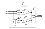
(第1の実施形態)
図7は、本発明の第1の実施形態に係る光パケットスイッチ装置10を説明するための図である。図7に示すように、光パケットスイッチ装置10は、光カプラ13と、光スイッチ部12と、光スイッチ制御部14とを備える。伝送路を経由して光パケットスイッチ装置10に入力された光パケット信号11は、光カプラ13で2つに分岐される。光パケット信号は、例えば10GEther等の光パケット信号であってよい。
(First embodiment)
FIG. 7 is a diagram for explaining the optical
分岐された一方の光パケット信号11aは、光スイッチ制御部14に入力され、他方の光パケット信号11bは、光遅延線34を介して光スイッチ部12に入力される。光スイッチ制御部14は、光パケット信号11aから方路情報を抽出し、該方路情報に応じて光スイッチ部12を制御する。光スイッチ部12は、光スイッチ制御部14からの光スイッチ制御信号に基づいて光パケット信号11bの方路を切り替えて出力する。
One of the branched optical packet signals 11 a is input to the optical
図7に示すように、光スイッチ制御部14は、光電変換部16と、シリアル/パラレル変換部18と、並び検出部17と、並び換え部19と、フレーム同期部20と、クロック乗換部22と、方路検出部24と、制御信号生成部26と、ローカル発振器28と、クロック逓倍部25と、タイミング調整部27とを備える。
As shown in FIG. 7, the optical
光電変換部16は、受信した光パケット信号11aを光電変換した後、増幅、クロック抽出、識別再生などの所定の処理を施して、データ信号DTとクロック信号CLK1をシリアル/パラレル変換部18に出力する。
The
シリアル/パラレル変換部18は、データ信号DTをシリアル/パラレル変換して、パラレルデータ信号DTSを出力すると共に、クロック信号CLK1を分周して分周クロック信号CLK2を出力する。本実施形態では、シリアル/パラレル変換部18は、1:8のシリアル/パラレル変換を行う。例えば、シリアル/パラレル変換部18に10Gbpsのデータ信号DTと、10GHzのクロック信号CLK1が入力される場合、1.25Gbps×8本のパラレルデータ信号DTSと、1.25GHzの分周クロック信号CLK2とがシリアル/パラレル変換部18から出力される。
The serial /
シリアル/パラレル変換部18から出力されたパラレルデータ信号DTSと分周クロック信号CLK2は、並び換え部19に入力される。また、パラレルデータ信号DTSと分周クロック信号CLK2は、並び検出部17にも入力される。並び検出部17は、パラレルデータ信号に含まれるフレーム同期パターンがどのような並びであるかを検出する。並び検出部17は、検出したフレーム同期パターンの並び情報を並び換え部19に出力する。並び換え部19は、該並び情報に基づいて、フレーム同期パターンが同一位相に並ぶようパラレルデータ信号を並び換える。また、本実施形態においては、並び検出部17からのフレーム同期パターンの並び情報は、タイミング調整部27にも出力される。
The parallel data signal DTS and the divided clock signal CLK2 output from the serial /
並び換え部19によって並び換えられたパラレルデータ信号DTSと分周クロック信号CLK2は、フレーム同期部20に入力される。フレーム同期部20は、所定のフレーム同期パターンを検出することで、光パケット信号のフレーム同期を確立する。
The parallel data signal DTS and the divided clock signal CLK2 rearranged by the
フレーム同期が取られたパラレルデータ信号DTSと分周クロック信号CLK2は、クロック乗換部22に入力される。クロック乗換部22は、分周クロック信号CLK2に同期したパラレルデータ信号DTSを、ローカル発振器28の出力するローカルクロック信号CLK3への乗せ換える。ローカルクロック信号CLK3は、分周クロック信号CLK2と同じ周波数のクロック信号である。
The parallel data signal DTS and the frequency-divided clock signal CLK2 that are frame-synchronized are input to the
クロック乗換部22から出力されたパラレルデータ信号DTSとローカルクロック信号CLK3は、方路検出部24に入力される。方路検出部24は受信したパラレルデータ信号DTSから方路情報を検出する。
The parallel data signal DTS and the local clock signal CLK3 output from the
制御信号生成部26は、方路検出部24により検出された方路情報に従って、光スイッチ部12内の光スイッチの開閉を制御するための光スイッチ制御信号を生成する。生成された光スイッチ制御信号は、タイミング調整部27に入力される。
The
タイミング調整部27は、並び換え部19からのフレーム同期パターンの並び情報に基づいて、制御信号生成部26からの光スイッチ制御信号を光スイッチ部12に出力するタイミングを調整する。この際、タイミング調整部27は、クロック逓倍部25によりローカルクロック信号CLKが逓倍された逓倍クロック信号CLK4を用いて、光スイッチ制御信号の出力タイミングを調整する。クロック逓倍部25は、PLL回路などを用いて構成できる。
The
一方、分岐された他方の光パケット信号11bは、光遅延線34を通った後、光スイッチ部12に入力される。光スイッチ部12は、入力された光パケット信号11bを2つに分岐する光カプラ30と、分岐された光パケット信号を受ける第1光スイッチ32aおよび第2光スイッチ32bとを備える、1×2の光スイッチである。第1光スイッチ32aおよび第2光スイッチ32bは、制御信号生成部26からの光スイッチ制御信号によりオン/オフを制御される。
On the other hand, the other branched
図8は、第1の実施形態におけるタイミング調整部の構成を説明するための図である。図8に示すように、タイミング調整部27は、セレクタ36と、第1〜第3フリップフロップ38a〜38cとを備える。
FIG. 8 is a diagram for explaining the configuration of the timing adjustment unit in the first embodiment. As illustrated in FIG. 8, the
制御信号生成部26で生成された光スイッチ制御信号は、直接セレクタ36に入力される。ここでは、この光スイッチ制御信号を「タイミング1」の光スイッチ制御信号と呼ぶ。
The optical switch control signal generated by the
第1フリップフロップ38aには、制御信号生成部26からの光スイッチ制御信号とクロック逓倍部25によりローカルクロック信号CLK3が4逓倍された逓倍クロック信号CLK4とが入力される。例えば、ローカルクロック信号CLK3が1.25GHzの場合、逓倍クロック信号CLK4は5GHzとなる。第1フリップフロップ38aに入力された光スイッチ制御信号は、タイミング1の光スイッチ制御信号と比べて逓倍クロック信号CLK4の1クロック分遅延され、セレクタ36に出力される。ここでは、この光スイッチ制御信号を「タイミング2」の光スイッチ制御信号と呼ぶ。
The first flip-
第2フリップフロップ38bには、第1フリップフロップ38aからの光スイッチ制御信号と逓倍クロック信号CLK4とが入力される。第2フリップフロップ38bに入力された光スイッチ制御信号は、逓倍クロック信号CLK4の1クロック分遅延され、セレクタ36に出力される。つまり、第2フリップフロップ38bからの光スイッチ制御信号は、タイミング1の光スイッチ制御信号と比べて、逓倍クロック信号CLK4の2クロック分遅延している。ここでは、この光スイッチ制御信号を「タイミング3」の光スイッチ制御信号と呼ぶ。
The second flip-
第3フリップフロップ38cには、第2フリップフロップ38bからの光スイッチ制御信号と逓倍クロック信号CLK4とが入力される。第3フリップフロップ38cに入力された光スイッチ制御信号は、逓倍クロック信号CLK4の1クロック分遅延され、セレクタ36に入力される。つまり、第3フリップフロップ38cからの光スイッチ制御信号は、タイミング1の光スイッチ制御信号と比べて、逓倍クロック信号CLK4の3クロック分遅延している。ここでは、この光スイッチ制御信号を「タイミング4」の光スイッチ制御信号と呼ぶ。
The third flip-
また、セレクタ36には、並び検出部17からフレーム同期パターンの並び情報が入力される。セレクタ36は、入力された並び情報からシリアルデータ信号DTと分周クロック信号CLK2との位相関係を判定する。そして、該判定結果に基づいてタイミング1〜4のスイッチ制御信号の中から一つを選択し、光スイッチ部12に出力する。
In addition, the
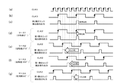
図9(a)〜(f)は、第1の実施形態に係る光パケットスイッチ装置10の動作を説明するためのタイムチャートである。図9(a)は、シリアルデータ信号DTから抽出されたクロック信号CLK1を示し、図9(b)は、クロック信号CLK1を分周した分周クロック信号CLK2を示す。なお、図9(a)〜(f)では、分周クロック信号CLK2は、クロック信号CLK1を8分周したものとして説明する。例えば、クロック信号CLK1を10GHzとした場合、分周クロック信号CLK2は1.25GHzとなる。
FIGS. 9A to 9F are time charts for explaining the operation of the optical
図9(c)は、分周クロック信号CLK2の立ち上がりエッジとシリアルデータ信号DTにおけるフレーム同期パターンB1の位相が合ったことにより、フレーム同期パターンB1〜B8が同一位相に並ぶようシリアル/パラレル変換されたケースを示す。このケースを「ケース1」と呼ぶ。なお、シリアルデータ信号DTおよびパラレルデータDTSは、フレーム同期パターンのみ図示している。
FIG. 9C shows the serial / parallel conversion so that the frame synchronization patterns B1 to B8 are arranged in the same phase because the rising edge of the divided clock signal CLK2 matches the phase of the frame synchronization pattern B1 in the serial data signal DT. Show the case. This case is referred to as “
図9(d)は、分周クロック信号CLK2の立ち上がりエッジとシリアルデータ信号DTにおけるフレーム同期パターンB3の位相が合ったことにより、フレーム同期パターンB3〜B8が同一位相に並び、フレーム同期パターンB1およびB2が分周クロック信号CLK2の1クロック分ずれた位相に並ぶようシリアル/パラレル変換されたケースを示す。このケースを「ケース2」と呼ぶ。
FIG. 9D shows that the frame synchronization pattern B3 to B8 are arranged in the same phase because the rising edge of the divided clock signal CLK2 and the phase of the frame synchronization pattern B3 in the serial data signal DT match, and the frame synchronization pattern B1 and A case where serial / parallel conversion is performed so that B2 is arranged in a phase shifted by one clock of the divided clock signal CLK2 is shown. This case is referred to as “
図9(e)は、分周クロック信号CLK2の立ち上がりエッジとシリアルデータ信号DTにおけるフレーム同期パターンB5の位相が合ったことにより、フレーム同期パターンB5〜B8が同一位相に並び、フレーム同期パターンB1〜B4が分周クロック信号CLK2の1クロック分ずれた位相に並ぶようシリアル/パラレル変換されたケースを示す。このケースを「ケース3」と呼ぶ。
FIG. 9 (e) shows that the frame synchronization patterns B5 to B8 are arranged in the same phase because the rising edge of the divided clock signal CLK2 and the phase of the frame synchronization pattern B5 in the serial data signal DT are matched. A case where serial / parallel conversion is performed so that B4 is arranged in a phase shifted by one clock of the divided clock signal CLK2 is shown. This case is referred to as “
図9(f)は、分周クロック信号CLK2の立ち上がりエッジとシリアルデータ信号DTにおけるフレーム同期パターンB7の位相が合ったことにより、フレーム同期パターンB7〜B8が同一位相に並び、フレーム同期パターンB1〜B6が分周クロック信号CLK2の1クロック分ずれた位相に並んだケースを示す。このケースを「ケース4」と呼ぶ。
FIG. 9 (f) shows that the frame synchronization patterns B7 to B8 are arranged in the same phase because the rising edge of the divided clock signal CLK2 and the phase of the frame synchronization pattern B7 in the serial data signal DT are matched. A case where B6 is arranged in a phase shifted by one clock of the divided clock signal CLK2 is shown. This case is referred to as “
ケース1〜4のようなフレーム同期パターンの並び方の違いは、シリアルデータ信号DTの位相と、分周クロック信号CLK2の位相関係が不定であることにより生じる。フレーム同期部20では、フレーム同期パターンB1〜B8が全て検出されたときにフレーム同期パルスが出力されるので、図9(c)〜(f)に示すように、フレーム同期パターンB1〜B8が同一位相に並ぶケース1と、フレーム同期パターンB1〜B8が分周クロック信号CLK2の2クロックに跨るケース2〜4とでは、フレーム同期パルスのタイミングが分周クロック信号CLK2の1クロック分ずれる。
The difference in how the frame synchronization patterns are arranged as in
そこで、本実施形態では、光スイッチ部12への出力タイミングを異ならせた4つ光スイッチ制御信号を用意しておく。またこれと並行して、並び検出部17からのフレーム同期パターンの並び情報に基づいて、シリアルデータ信号DTと分周クロック信号CLK2との位相関係がケース1〜4のどのケースに該当するか判定する。そして、この判定結果に応じてタイミング1〜4のスイッチ制御信号の中から一つを選択し、光スイッチ部12に出力する。
Therefore, in the present embodiment, four optical switch control signals having different output timings to the
本実施形態では、フレーム同期パターンがケース2のような並びの場合に、セレクタ36は、「タイミング1」の光スイッチ制御信号を選択する。ここで、制御信号生成部26は、フレーム同期パルスと光スイッチ制御信号との位相差が「0」となるように、光スイッチ制御信号を出力する。言い換えると、フレーム同期パターンの立ち下がりエッジと、光スイッチ制御信号の出力タイミングとの位相差が「0」となるように光スイッチ制御信号を出力する。このケース2の光スイッチ制御信号の出力タイミングを基準として、他のケースの光スイッチ制御信号の出力タイミングを調整する。
In the present embodiment, when the frame synchronization patterns are arranged as in
フレーム同期パターンが「ケース3」のように並んでいる場合、セレクタ36は、「タイミング2」の光スイッチ制御信号を選択し、光スイッチ部12に出力する。この場合、図9(e)に示すように、セレクタ36からはフレーム同期パルスの立ち下がりエッジから逓倍クロック信号CLK4の1クロック分遅延したスイッチ制御信号が出力される。
When the frame synchronization patterns are arranged like “
フレーム同期パターンが「ケース4」のように並んでいる場合、セレクタ36は、「タイミング3」の光スイッチ制御信号を選択し、光スイッチ部12に出力する。この場合、図9(f)に示すように、セレクタ36からはフレーム同期パルスの立ち下がりエッジから逓倍クロック信号CLK4の2クロック分遅延したスイッチ制御信号が出力される。
When the frame synchronization patterns are arranged like “
フレーム同期パターンが「ケース1」のように並んでいる場合、セレクタ36は、「タイミング4」の光スイッチ制御信号を選択し、光スイッチ部12に出力する。この場合、図9(c)に示すように、セレクタ36からはフレーム同期パルスの立ち下がりエッジから逓倍クロック信号CLK4の3クロック分遅延した光スイッチ制御信号が出力される。
When the frame synchronization patterns are arranged like “
本実施形態に係る光パケットスイッチ装置10によれば、図9(c)〜(f)に示すように、光パケット信号が光スイッチ部12に入力するタイミングに合わせて、光スイッチをオン状態にすることができる。これにより、光スイッチオン時間を上述の比較例と比べて短くできる。
According to the optical
なお、シリアルデータ信号DTと分周クロック信号CLK2の位相関係によっては、フレーム同期パターンの並びがケース1〜4に正確には当てはまらない場合もある。この場合、セレクタ36は、例えば最も並び方の近いケースを判定し、該ケースに対応する光スイッチ制御信号を選択する。
Note that, depending on the phase relationship between the serial data signal DT and the divided clock signal CLK2, the arrangement of the frame synchronization patterns may not be accurately applied to
以上説明したように、本実施形態に係る光パケットスイッチ装置10では、タイミング調整部27に出力タイミングを異ならせた4つの光スイッチ制御信号を用意しておき、並び検出部17からのフレーム同期パターンの並び情報に基づいて最適なタイミングの光スイッチ制御信号を選択し、光スイッチ部12に出力するよう構成した。これにより、光スイッチオン時間を短くでき、ガードタイムを短くできるので、伝送路の帯域利用効率を向上できる。
As described above, in the optical
また、本実施形態では、ローカルクロック信号CLK3を逓倍した逓倍クロック信号CLK4を用いて、光スイッチ制御信号の出力タイミングを調整する構成とした。これにより、ローカルクロック信号CLK3の変化点に同期して光スイッチ制御信号を出力する場合と比較して、光スイッチの開閉タイミングの分解能を高めることができるので、余分な光スイッチオン時間を削減できる。 In the present embodiment, the output timing of the optical switch control signal is adjusted by using the multiplied clock signal CLK4 obtained by multiplying the local clock signal CLK3. Thereby, compared with the case where the optical switch control signal is output in synchronization with the changing point of the local clock signal CLK3, the resolution of the opening / closing timing of the optical switch can be increased, so that the extra optical switch on time can be reduced. .
(第2の実施形態)
図10は、本発明の第2の実施形態に係る光パケットスイッチ装置10を説明するための図である。本実施形態に係る光パケットスイッチ装置10において、図7に示す第1の実施形態に係る光パケットスイッチ装置10と同一または対応する構成要素については、同一の符号を付すと共に、詳細な説明を適宜省略する。
(Second Embodiment)
FIG. 10 is a diagram for explaining an optical
図10に示すように、本実施形態に係る光パケットスイッチ装置10は、クロック乗換部22に入力される分周クロック信号CLK2とローカルクロック信号CLK3の位相差を検出する位相差検出部29を備える。クロック乗換部22において、分周クロック信号CLK2は書込クロックであり、ローカルクロック信号CLK3は読出クロックである。位相差検出部29は、ローカルクロック信号CLK3をクロック逓倍部25にて逓倍した逓倍クロック信号CLK4を用いて、分周クロック信号CLK2とローカルクロック信号CLK3の位相差を検出する。そして、位相差検出部29にて検出された位相差情報は、タイミング調整部27に送られる。
As illustrated in FIG. 10, the optical
タイミング調整部27は、位相差検出部29により検出された位相差情報に基づいて、制御信号生成部26からの光スイッチ制御信号を光スイッチ部12に出力するタイミングを調整する。この際、タイミング調整部27は、逓倍クロック信号CLK4を用いて光スイッチ制御信号の出力タイミングを調整する。
The
図11は、第2の実施形態における位相差検出部29およびタイミング調整部27の構成を説明するための図である。
FIG. 11 is a diagram for explaining the configuration of the phase
図11に示すように、位相差検出部29は、第1微分エッジ検出部42と、第2微分エッジ検出部44と、位相差判定部40とを備える。
As shown in FIG. 11, the phase
第1微分エッジ検出部42は、入力された分周クロック信号CLK2を微分することにより、分周クロック信号CLK2の立ち上がりエッジを検出する。第1微分エッジ検出部42は、フリップフロップ42aおよび42bと、論理積(AND)部42cとを備える。フリップフロップ42aには、分周クロック信号CLK2と、逓倍クロック信号CLK4とが入力される。フリップフロップ42bには、フリップフロップ42aの出力と、逓倍クロック信号CLK4とが入力される。論理積部42cには、フリップフロップ42aの出力と、フリップフロップ42bの反転出力とが入力される。論理積部42cの出力は、位相差判定部40に入力される。
The first differential edge detector 42 detects the rising edge of the divided clock signal CLK2 by differentiating the input divided clock signal CLK2. The first differential edge detection unit 42 includes flip-
第2微分エッジ検出部44は、入力されたローカルクロック信号CLK3を微分することにより、ローカルクロック信号CLK3の立ち上がりエッジを検出する。第2微分エッジ検出部44は、フリップフロップ44aおよび44bと、論理積部44cとを備える。フリップフロップ44aには、ローカルクロック信号CLK3と、逓倍クロック信号CLK4とが入力される。フリップフロップ44bには、フリップフロップ44aの出力と、逓倍クロック信号CLK4とが入力される。論理積部44cには、フリップフロップ44aの出力と、フリップフロップ44bの反転出力とが入力される。論理積部44cの出力は、位相差判定部40に入力される。
The second differential
なお、本実施形態では、第1微分エッジ検出部42および第2微分エッジ検出部44は、クロック信号の立ち上がりエッジを検出する構成としたが、立ち下がりエッジを検出する構成としてもよい。
In the present embodiment, the first differential edge detector 42 and the second
位相差判定部40は、第1微分エッジ検出部42からの出力パルスと、第2微分エッジ検出部44からの出力パルスとの間の位相差を、逓倍クロック信号CLK4を用いて判定する。位相差判定部40で検出された位相差情報は、タイミング調整部27のセレクタ36に出力される。
The phase
タイミング調整部27は、セレクタ36と、第1〜第3フリップフロップ38a〜38cとを備える。本実施形態において、制御信号生成部26で生成された光スイッチ制御信号は、直接セレクタ36に入力される。ここでは、この光スイッチ制御信号を「タイミング1」の光スイッチ制御信号と呼ぶ。
The
第1フリップフロップ38aには、制御信号生成部26からの光スイッチ制御信号と逓倍クロック信号CLK4とが入力される。第1フリップフロップ38aに入力された光スイッチ制御信号は、タイミング1の光スイッチ制御信号と比べて逓倍クロック信号CLK4の1クロック分遅延され、セレクタ36に出力される。ここでは、この光スイッチ制御信号を「タイミング2」の光スイッチ制御信号と呼ぶ。
The first flip-
第2フリップフロップ38bには、第1フリップフロップ38aからの光スイッチ制御信号と逓倍クロック信号CLK4とが入力される。第2フリップフロップ38bからの光スイッチ制御信号は、タイミング1の光スイッチ制御信号と比べて、逓倍クロック信号CLK4の2クロック分遅延している。ここでは、この光スイッチ制御信号を「タイミング3」の光スイッチ制御信号と呼ぶ。
The second flip-
第3フリップフロップ38cには、第2フリップフロップ38bからの光スイッチ制御信号と逓倍クロック信号CLK4とが入力される。第3フリップフロップ38cからの光スイッチ制御信号は、タイミング1の光スイッチ制御信号と比べて、逓倍クロック信号CLK4の3クロック分遅延している。ここでは、この光スイッチ制御信号を「タイミング4」の光スイッチ制御信号と呼ぶ。
The third flip-
セレクタ36は、位相差判定部40からの位相差情報に基づいて、タイミング1〜4の光スイッチ制御信号の中から最適な出力タイミングの光スイッチ制御信号を選択し、光スイッチ部12に出力する。
Based on the phase difference information from the phase
図12(a)〜(g)は、第2の実施形態に係る光パケットスイッチ装置10の動作を説明するためのタイムチャートである。図12(a)は、逓倍クロック信号を示し、図12(b)は、ローカルクロック信号CLK3を示し、図12(c)は、第2微分エッジ検出部44の出力を示す。なお、図12(a)〜(g)では、逓倍クロック信号CLK4は、ローカルクロック信号CLK3を4逓倍したものとして説明する。例えば、ローカルクロック信号CLK3を1.25GHzとした場合、逓倍クロック信号CLK4は5GHzとなる。
FIGS. 12A to 12G are time charts for explaining the operation of the optical
図12(c)に示すように、第2微分エッジ検出部44は、ローカルクロック信号CLK3の立ち上がりエッジに同期したパルスを出力する。本実施形態において、位相差判定部40は、この第2微分エッジ検出部44の出力パルスの位相を基準位相として、第1微分エッジ検出部42の出力パルスの位相が基準位相から逓倍クロック信号CLK4の何クロック分前に位置するか判定することで、分周クロック信号CLK2とローカルクロック信号CLK3との位相差を判定する。
As shown in FIG. 12C, the second
図12(d)は、分周クロック信号CLK2とローカルクロック信号CLK3の位相差が0°のケース1を示す。このケース1において、第1微分エッジ検出部42の出力パルスと第2微分エッジ検出部44の出力パルスは同位相である。ケース1の場合、クロック乗換部22における伝搬遅延時間は最短となる。
FIG. 12D shows
図12(e)は、分周クロック信号CLK2とローカルクロック信号CLK3の位相差が270°のケース2を示す。このケース2において、第1微分エッジ検出部42の出力パルスは、基準位相よりも逓倍クロック信号CLK4の3CLK前に存在するので、分周クロック信号CLK2とローカルクロック信号CLK3の位相差は270°となる。ケース2の場合、クロック乗換部22における伝搬遅延時間は、ケース1よりも逓倍クロック信号CLK4の3クロック分長くなる。
FIG. 12E shows
図12(f)は、分周クロック信号CLK2とローカルクロック信号CLK3の位相差が180°のケース3を示す。このケース3において、第1微分エッジ検出部42の出力パルスは、基準位相よりも逓倍クロック信号CLK4の2CLK前に存在するので、分周クロック信号CLK2の位相は、ローカルクロック信号CLK3の位相よりも180°遅延している。ケース3の場合、クロック乗換部22における伝搬遅延時間は、ケース1よりも逓倍クロック信号CLK4の2クロック分長くなる。
FIG. 12F shows
図12(g)は、分周クロック信号CLK2とローカルクロック信号CLK3の位相差が270°のケース4を示す。このケース4において、第1微分エッジ検出部42の出力パルスは、基準位相よりも逓倍クロック信号CLK4の1CLK前に存在するので、分周クロック信号CLK2の位相は、ローカルクロック信号CLK3の位相よりも90°遅延している。ケース4の場合、クロック乗換部22における伝搬遅延時間は、ケース1よりも逓倍クロック信号CLK4の1クロック分長くなる。
FIG. 12G shows
位相差判定部40は、分周クロック信号CLK2とローカルクロック信号CLK3の位相差がケース1〜4のいずれに該当するか判定し、該判定結果を位相差情報としてセレクタ36に出力する。分周クロック信号CLK2とローカルクロック信号CLK3の位相関係は不定であるので、ケース1〜4に正確に一致しない場合もある。この場合、位相差判定部40は、例えば最も位相差の近いケースを判定し、判定結果をセレクタ36に出力する。
The phase
位相差判定部40から分周クロック信号CLK2とローカルクロック信号CLK3の位相差が0°(ケース1)という情報が入力された場合、セレクタ36は、タイミング1の光スイッチ制御信号を選択し、光スイッチ部12に出力する。
When the information that the phase difference between the divided clock signal CLK2 and the local clock signal CLK3 is 0 ° (case 1) is input from the phase
位相差判定部40から分周クロック信号CLK2とローカルクロック信号CLK3の位相差が90°(ケース4)という情報が入力された場合、セレクタ36は、タイミング2の光スイッチ制御信号を選択し、光スイッチ部12に出力する。
When the information that the phase difference between the divided clock signal CLK2 and the local clock signal CLK3 is 90 ° (case 4) is input from the phase
位相差判定部40から分周クロック信号CLK2とローカルクロック信号CLK3の位相差が180°(ケース3)という情報が入力された場合、セレクタ36は、タイミング3の光スイッチ制御信号を選択し、光スイッチ部12に出力する。
When information indicating that the phase difference between the divided clock signal CLK2 and the local clock signal CLK3 is 180 ° (case 3) is input from the phase
位相差判定部40から分周クロック信号CLK2とローカルクロック信号CLK3の位相差が270°(ケース2)という情報が入力された場合、セレクタ36は、タイミング4の光スイッチ制御信号を選択し、光スイッチ部12に出力する。
When information indicating that the phase difference between the divided clock signal CLK2 and the local clock signal CLK3 is 270 ° (case 2) is input from the phase
このように、タイミング1〜4の光スイッチ制御信号を用意しておき、位相差検出部29からの位相差情報に基づいて、最適なタイミングの光スイッチ制御信号を選択することで、光パケット信号が光スイッチ部12に入力するタイミングに合わせて、光スイッチをオン状態にすることができる。これにより、光スイッチオン時間を上述の比較例と比べて短くできる。
In this way, the optical switch control signal at
また、本実施形態においても、ローカルクロック信号CLK3を逓倍した逓倍クロック信号CLK4を用いて、光スイッチ制御信号の出力タイミングを調整する構成とした。これにより、ローカルクロック信号CLK3の変化点に同期して光スイッチ制御信号を出力する場合と比較して、光スイッチの開閉タイミングの分解能を高めることができるので、余分な光スイッチオン時間を削減できる。 Also in this embodiment, the output timing of the optical switch control signal is adjusted using the multiplied clock signal CLK4 obtained by multiplying the local clock signal CLK3. Thereby, compared with the case where the optical switch control signal is output in synchronization with the changing point of the local clock signal CLK3, the resolution of the opening / closing timing of the optical switch can be increased, so that the extra optical switch on time can be reduced. .
図13は、位相差検出部の変形例を示す。図13に示すように、本変形例に係る位相差検出部29は、第1排他的論理和部(X−OR)46と、第2排他的論理和部52と、第1ローパスフィルタ(LPF)48と、第2ローパスフィルタ54と、第1コンパレータ50と、第2コンパレータ56と、90°位相遅延部(DL)58と、位相差判定部40とを備える。
FIG. 13 shows a modification of the phase difference detection unit. As illustrated in FIG. 13, the phase
第1排他的論理和部46には、分周クロック信号CLK2と、ローカルクロック信号CLK3とが入力される。第1排他的論理和部46は、分周クロック信号CLK2とローカルクロック信号CLK3の排他的論理和信号(以下、「第1排他的論理和信号X−OR1」と呼ぶ)を第1ローパスフィルタ48に出力する。また、第2排他的論理和部52には、分周クロック信号CLK2と、90°位相遅延部により位相が90°遅延したローカルクロック信号CLK3(以下、「遅延ローカルクロック信号CLK3−DLY」と呼ぶ)が入力される。第2排他的論理和部52は、分周クロック信号CLK2と、遅延ローカルクロック信号CLK3−DLYの排他的論理和信号(以下、「第2排他的論理和信号X−OR2」と呼ぶ)を第2ローパスフィルタ54に出力する。
A frequency-divided clock signal CLK2 and a local clock signal CLK3 are input to the first exclusive OR
なお、第2排他的論理和部52には、ローカルクロック信号CLK3と、90°位相遅延部により位相が90°遅延した分周クロック信号CLK2が入力されてもよい。
The second exclusive OR
図14は、分周クロック信号とローカルクロック信号間の位相差(以下、「クロック間位相差」と呼ぶ)と、排他的論理和信号のデューティ(Duty)比の関係を示す図である。図14において、実線は、クロック間位相差と、第1排他的論理和信号X−ORのデューティ比との関係を示す。また、一点鎖線は、クロック間位相差と、第2排他的論理和信号X−OR2のデューティ比との関係を示す。 FIG. 14 is a diagram illustrating the relationship between the phase difference between the divided clock signal and the local clock signal (hereinafter referred to as “clock phase difference”) and the duty ratio of the exclusive OR signal. In FIG. 14, the solid line indicates the relationship between the clock phase difference and the duty ratio of the first exclusive OR signal X-OR. The alternate long and short dash line indicates the relationship between the phase difference between clocks and the duty ratio of the second exclusive OR signal X-OR2.
図14に示すように、クロック間位相差に応じて、第1排他的論理和信号X−ORと第2排他的論理和信号X−OR2は共にデューティ比が変化するが、その変化の仕方は異なる。第1排他的論理和信号X−ORと第2排他的論理和信号X−OR2のデューティ比を参照することで、クロック間位相差が、1:0〜90°の範囲、2:90〜180°の範囲、3:180〜270°の範囲、4:270〜360°の範囲、のいずれに属するか判定することができる。 As shown in FIG. 14, the duty ratios of the first exclusive OR signal X-OR and the second exclusive OR signal X-OR2 change according to the phase difference between the clocks. Different. By referring to the duty ratio of the first exclusive OR signal X-OR and the second exclusive OR signal X-OR2, the phase difference between clocks is in the range of 1: 0 to 90 °, 2:90 to 180. It can be determined whether it belongs to the range of °, 3: 180 to 270 °, or 4: 270 to 360 °.
より詳細に説明すると、第1排他的論理和信号X−OR1のデューティ比が0.5未満、且つ第2排他的論理和信号X−OR2のデューティ比が0.5以上のとき、クロック間位相差は、0〜90°の範囲に属すると判定できる。また、第1排他的論理和信号X−OR1のデューティ比が0.5以上、且つ第2排他的論理和信号X−OR2のデューティ比が0.5以上のとき、クロック間位相差は、90〜180°の範囲に属すると判定できる。また、第1排他的論理和信号X−OR1のデューティ比が0.5以上、且つ第2排他的論理和信号X−OR2のデューティ比が0.5未満のとき、クロック間位相差は、180〜270°の範囲に属すると判定できる。また、第1排他的論理和信号X−OR1のデューティ比が0.5未満、且つ第2排他的論理和信号X−OR2のデューティ比が0.5未満のとき、クロック間位相差は、270〜360°の範囲に属すると判定できる。 More specifically, when the duty ratio of the first exclusive OR signal X-OR1 is less than 0.5 and the duty ratio of the second exclusive OR signal X-OR2 is 0.5 or more, the clock interval It can be determined that the phase difference belongs to a range of 0 to 90 °. When the duty ratio of the first exclusive OR signal X-OR1 is 0.5 or more and the duty ratio of the second exclusive OR signal X-OR2 is 0.5 or more, the phase difference between clocks is 90 It can be determined that it belongs to the range of ˜180 °. When the duty ratio of the first exclusive OR signal X-OR1 is 0.5 or more and the duty ratio of the second exclusive OR signal X-OR2 is less than 0.5, the phase difference between clocks is 180. It can be determined that it belongs to the range of ˜270 °. When the duty ratio of the first exclusive OR signal X-OR1 is less than 0.5 and the duty ratio of the second exclusive OR signal X-OR2 is less than 0.5, the inter-clock phase difference is 270. It can be determined that it belongs to the range of ~ 360 °.
図13に戻るが、上述のような判定を行うために、本変形例に係る位相差検出部29では、第1排他的論理和信号X−OR1を第1ローパスフィルタ48に入力し、第1排他的論理和信号X−OR1の平均電圧を求める。そして、該平均電圧を第1コンパレータ50に入力し、所定の基準電圧Vrefと比較する。基準電圧Vrefは、デューティ比を0.5とした排他的論理和信号の平均電圧に設定する。また、第2排他的論理和信号X−OR2を第2ローパスフィルタ54に入力し、第2排他的論理和信号X−OR2の平均電圧を求める。そして、該平均電圧を第2コンパレータ56に入力し、基準電圧Vrefと比較する。第1コンパレータ50と第2コンパレータ56の出力信号は、位相差判定部40に入力される。
Returning to FIG. 13, in order to perform the above-described determination, the phase
位相差判定部40は、第1コンパレータ50と第2コンパレータ56からの入力信号を参照することで、クロック間位相差が上記4つの範囲のいずれに属するか判定する。位相差判定部40により判定された位相差情報は、図11で説明したタイミング調整部27のセレクタ36に送られる。タイミング調整部27は、例えば、クロック間位相差が0〜90°の範囲に属する場合、タイミング1の光スイッチ制御信号を選択する。また、クロック間位相差が90〜180°の範囲に属する場合、タイミング2の光スイッチ制御信号を選択する。また、クロック間位相差が180〜270°の範囲に属する場合、タイミング3の光スイッチ制御信号を選択する。また、クロック間位相差が270〜360°の範囲に属する場合、タイミング4の光スイッチ制御信号を選択する。
The phase
図15は、位相差検出部の別の変形例を示す。図15に示すように、本変形例に係る位相差検出部29は、図13に示す位相差検出部における第1排他的論理和部46、第2排他的論理和部52を、それぞれ第1論理積部60、第2論理積部62に置き換えたものである。また、本変形例においては、基準電圧Vrefは、デューティ比を0.25とした論理積信号の平均電圧に設定する。本変形例に係る位相差検出部29によっても、図13に示す位相差検出部と類似の方法により、クロック間位相差が属する範囲を検出できる。
FIG. 15 shows another modification of the phase difference detection unit. As illustrated in FIG. 15, the phase
図16は、位相差検出部のさらに別の変形例を示す。図16に示すように、本変形例に係る位相差検出部29は、図13に示す位相差検出部における第1排他的論理和部46、第2排他的論理和部52を、それぞれ第1論理和部64、第2論理和部66に置き換えたものである。また、本変形例においては、基準電圧Vrefは、デューティ比を0.75とした論理和信号の平均電圧に設定する。本変形例に係る位相差検出部29によっても、図13に示す位相差検出部と類似の方法により、クロック間位相差が属する範囲を検出できる。
FIG. 16 shows still another modification of the phase difference detection unit. As illustrated in FIG. 16, the phase
(第3の実施形態)
図17は、本発明の第3の実施形態に係る光パケットスイッチ装置10を説明するための図である。本実施形態に係る光パケットスイッチ装置10において、図7に示す第1の実施形態に係る光パケットスイッチ装置と同一または対応する構成要素については、同一の符号を付すと共に、詳細な説明を適宜省略する。
(Third embodiment)
FIG. 17 is a diagram for explaining an optical
本実施形態に係る光パケットスイッチ装置10は、図7に示す第1の実施形態と図10に示す第2の実施形態を組み合わせた構成となっている。本実施形態に係る光パケットスイッチ装置10は、2つのタイミング調整部(第1タイミング調整部68および第2タイミング調整部70)を備える。
The optical
図17に示すように、並び検出部17からのフレーム同期パターンの並び情報は、第1タイミング調整部68に入力される。また、位相差検出部29からの位相差情報は、第2タイミング調整部70に入力される。また、第1タイミング調整部68、第2タイミング調整部70には、クロック逓倍部25から逓倍クロック信号CLK4が入力される。
As shown in FIG. 17, the frame synchronization pattern arrangement information from the
本実施形態において、制御信号生成部26で生成された光スイッチ制御信号は、まず第1タイミング調整部68に入力される。第1タイミング調整部68は、フレーム同期パターンの並び情報に基づいて、光スイッチ制御信号の出力タイミングを調整する。調整方法は、第1の実施形態に係る光パケットスイッチ装置と同様である。第1タイミング調整部68により調整された光スイッチ制御信号は、次に第2タイミング調整部70に出力される。第2タイミング調整部70は、分周クロック信号CLK2とローカルクロック信号CLK3の位相差情報に基づいて、光スイッチ制御信号の出力タイミングをさらに調整する。調整方法は、第2の実施形態に係る光パケットスイッチ装置と同様である。第2タイミング調整部70にて調整された光スイッチ制御信号は、光スイッチ部12に出力される。
In the present embodiment, the optical switch control signal generated by the control
本実施形態に係る光パケットスイッチ装置10によれば、並び検出部17からの並び情報に加えて、位相差検出部29からの位相差情報を用いて光スイッチ制御信号の出力タイミングを調整することで、上述した第1および第2の実施形態よりも最適なタイミングで光スイッチ制御信号を光スイッチ部12に出力できる。これにより、光スイッチオン時間をより短くできるので、伝送路の帯域利用効率をさらに向上できる。
According to the optical
以上、本発明を実施の形態をもとに説明した。この実施の形態は例示であり、それらの各構成要素や各処理プロセスの組合せによりいろいろな変形例が可能なこと、またそうした変形例も本発明の範囲にあることは当業者に理解されるところである。 The present invention has been described based on the embodiments. This embodiment is an exemplification, and it will be understood by those skilled in the art that various modifications are possible depending on the combination of each component and each processing process, and such modifications are within the scope of the present invention. is there.
例えば、上述したシリアル/パラレル変換の変換比や、逓倍クロック信号の逓倍比などは一例であり、特に限定されない。逓倍比を高めることができれば、それだけ光スイッチ開閉タイミングの分解能を高めることができる。 For example, the conversion ratio of the serial / parallel conversion described above and the multiplication ratio of the multiplied clock signal are examples, and are not particularly limited. If the multiplication ratio can be increased, the resolution of the optical switch opening / closing timing can be increased accordingly.
10 光パケットスイッチ装置、 12 光スイッチ部、 13 光カプラ、 14 光スイッチ制御部、 17 並び検出部、 19 並び換え部、 20 フレーム同期部、 22 クロック乗換部、 25 クロック逓倍部、 26 制御信号生成部、 27 タイミング調整部、 28 ローカル発振器、 29 位相差検出部、 34 光遅延線、 36 セレクタ、 40 位相差判定部、 42 第1微分エッジ検出部、 44 第2微分エッジ検出部、 46 第1排他的論理和部、 48 第1ローパスフィルタ48、 50 第1コンパレータ、 52 第2排他的論理和部、 56 第2コンパレータ、 60 第1論理積部、 62 第2論理積部、 64 第1論理和部、 66 第2論理和部、 68 第1タイミング調整部、 70 第2タイミング調整部。
DESCRIPTION OF
Claims (15)
分岐された一方の光パケット信号の方路を切り替えて出力する光スイッチ部と、
分岐された他方の光パケット信号から方路情報を抽出し、該方路情報に応じて前記光スイッチ部を制御する光スイッチ制御部と、
を備える光パケットスイッチ装置であって、
前記光スイッチ制御部は、
前記他方の光パケット信号を電気のデータ信号に変換すると共に、該データ信号からクロック信号を抽出する光電変換部と、
前記データ信号をパラレルデータ信号にシリアル/パラレル変換すると共に、前記クロック信号を分周して分周クロック信号を生成するシリアル/パラレル変換部と、
前記パラレルデータ信号に含まれるフレーム同期パターンの並びを検出する並び検出部と、
検出されたフレーム同期パターンの並び情報に基づいて、前記パラレルデータ信号の並び換えを行う並び換え部と、
並び換えられたパラレルデータ信号に含まれるフレーム同期パターンに基づいてフレーム同期を確立するフレーム同期部と、
フレーム同期が確立された後、前記パラレルデータ信号に含まれる方路情報を検出する方路検出部と、
検出された方路情報に基づいて、前記光スイッチ部を制御するための光スイッチ制御信号を生成する生成部と、
前記フレーム同期パターンの並び情報に基づいて、前記光スイッチ部に前記光スイッチ制御信号を出力するタイミングを調整する調整部と、
を備えることを特徴とする光パケットスイッチ装置。 A branching unit for branching the received optical packet signal;
An optical switch unit that switches and outputs the route of one of the branched optical packet signals;
An optical switch control unit that extracts route information from the other branched optical packet signal and controls the optical switch unit according to the route information;
An optical packet switch device comprising:
The optical switch controller is
A photoelectric converter that converts the other optical packet signal into an electrical data signal and extracts a clock signal from the data signal;
A serial / parallel converter that serially / parallel converts the data signal into a parallel data signal and divides the clock signal to generate a divided clock signal;
An arrangement detecting unit for detecting an arrangement of frame synchronization patterns included in the parallel data signal;
A rearrangement unit for rearranging the parallel data signals based on the detected frame synchronization pattern arrangement information;
A frame synchronization unit for establishing frame synchronization based on a frame synchronization pattern included in the rearranged parallel data signal;
After frame synchronization is established, a route detection unit that detects route information included in the parallel data signal;
A generating unit for generating an optical switch control signal for controlling the optical switch unit based on the detected route information;
An adjustment unit that adjusts the timing of outputting the optical switch control signal to the optical switch unit based on the arrangement information of the frame synchronization pattern;
An optical packet switch device comprising:
ローカルクロック信号を発振するローカル発振器と、
前記分周クロック信号に同期した前記パラレルデータ信号を前記ローカルクロック信号に乗せ換えるクロック乗換部と、
前記分周クロック信号と前記ローカルクロック信号の位相差を検出する位相差検出部と、
前記位相差検出部からの位相差情報に基づいて、光スイッチ制御信号の出力タイミングをさらに調整する第2の調整部と、
をさらに備えることを特徴とする請求項1から3のいずれかに記載の光パケットスイッチ装置。 The optical switch controller is
A local oscillator that oscillates the local clock signal;
A clock transfer section for transferring the parallel data signal synchronized with the divided clock signal to the local clock signal;
A phase difference detector for detecting a phase difference between the divided clock signal and the local clock signal;
A second adjustment unit for further adjusting the output timing of the optical switch control signal based on the phase difference information from the phase difference detection unit;
The optical packet switch device according to claim 1, further comprising:
前記分周クロック信号の立ち上がりエッジ又は立ち下がりエッジを微分エッジ検出する第1エッジ検出部と、
前記ローカルクロック信号の立ち上がりエッジ又は立ち下がりエッジを微分エッジ検出する第2エッジ検出部と、
前記第1エッジ検出部からの出力パルスと、前記第2エッジ検出部からの出力パルスとの間の位相差を判定する位相差判定部と、
を備えることを特徴とする請求項4に記載の光パケットスイッチ装置。 The phase difference detector is
A first edge detector for detecting a differential edge of a rising edge or a falling edge of the divided clock signal;
A second edge detector that detects a differential edge of a rising edge or a falling edge of the local clock signal;
A phase difference determination unit that determines a phase difference between an output pulse from the first edge detection unit and an output pulse from the second edge detection unit;
The optical packet switch device according to claim 4, further comprising:
前記分周クロック信号と前記ローカルクロック信号の排他的論理和を演算する第1排他的論理和部と、
前記分周クロック信号と前記ローカルクロック信号のいずれか一方の位相を90°遅らせたクロック信号と、他方のクロック信号との排他的論理を演算する第2排他的論理和部と、
前記第1排他的論理和部および前記第2排他的論理和部からの出力のデューティ比に基づいて、前記分周クロック信号と前記ローカルクロック信号との間の位相差を判定する位相差判定部と、
を備えることを特徴とする請求項4に記載の光パケットスイッチ装置。 The phase difference detector is
A first exclusive OR unit that calculates an exclusive OR of the divided clock signal and the local clock signal;
A second exclusive OR unit that calculates an exclusive logic of the clock signal obtained by delaying the phase of one of the divided clock signal and the local clock signal by 90 °, and the other clock signal;
A phase difference determination unit that determines a phase difference between the divided clock signal and the local clock signal based on a duty ratio of outputs from the first exclusive OR unit and the second exclusive OR unit When,
The optical packet switch device according to claim 4, further comprising:
前記分周クロック信号と前記ローカルクロック信号の論理積を演算する第1論理積部と、
前記分周クロック信号と前記ローカルクロック信号のいずれか一方の位相を90°遅らせたクロック信号と、他方のクロック信号との論理積を演算する第2論理積部と、
前記第1論理積部および前記第2論理積部からの出力のデューティ比に基づいて、前記分周クロック信号と前記ローカルクロック信号との間の位相差を判定する位相差判定部と、
を備えることを特徴とする請求項4に記載の光パケットスイッチ装置。 The phase difference detector is
A first AND section for calculating a logical product of the divided clock signal and the local clock signal;
A second logical product unit that calculates a logical product of a clock signal obtained by delaying the phase of one of the divided clock signal and the local clock signal by 90 ° and the other clock signal;
A phase difference determination unit that determines a phase difference between the divided clock signal and the local clock signal based on a duty ratio of outputs from the first AND unit and the second AND unit;
The optical packet switch device according to claim 4, further comprising:
前記分周クロック信号と前記ローカルクロック信号の論理和を演算する第1論理和部と、
前記分周クロック信号と前記ローカルクロック信号のいずれか一方の位相を90°遅らせたクロック信号と、他方のクロック信号との論理和を演算する第2論理和部と、
前記第1論理和部および前記第2論理和部からの出力のデューティ比に基づいて、前記分周クロック信号と前記ローカルクロック信号との間の位相差を判定する位相差判定部と、
を備えることを特徴とする請求項4に記載の光パケットスイッチ装置。 The phase difference detector is
A first OR circuit that calculates a logical sum of the divided clock signal and the local clock signal;
A second logical sum unit for calculating a logical sum of a clock signal obtained by delaying the phase of one of the divided clock signal and the local clock signal by 90 ° and the other clock signal;
A phase difference determining unit that determines a phase difference between the divided clock signal and the local clock signal based on a duty ratio of outputs from the first OR unit and the second OR unit;
The optical packet switch device according to claim 4, further comprising:
分岐された一方の光パケット信号の方路を切り替えて出力する光スイッチ部と、
分岐された他方の光パケット信号から方路情報を抽出し、該方路情報に応じて前記光スイッチ部を制御する光スイッチ制御部と、
を備える光パケットスイッチ装置であって、
前記光スイッチ制御部は、
前記他方の光パケット信号を電気のデータ信号に変換すると共に、該データ信号からクロック信号を抽出する光電変換部と、
前記データ信号をパラレルデータ信号にシリアル/パラレル変換すると共に、前記クロック信号を分周して分周クロック信号を生成するシリアル/パラレル変換部と、
ローカルクロック信号を発振するローカル発振器と、
前記分周クロック信号に同期した前記パラレルデータ信号を前記ローカルクロック信号に乗せ換えるクロック乗換部と、
前記パラレルデータ信号に含まれる方路情報を検出する方路検出部と、
検出された方路情報に基づいて、前記光スイッチ部を制御するための光スイッチ制御信号を生成する生成部と、
前記分周クロック信号と前記ローカルクロック信号の位相差を検出する位相差検出部と、
前記位相差検出部からの位相差情報に基づいて、光スイッチ制御信号の出力タイミングを調整する調整部と、
を備えることを特徴とする光パケットスイッチ装置。 A branching unit for branching the received optical packet signal;
An optical switch unit that switches and outputs the route of one of the branched optical packet signals;
An optical switch control unit that extracts route information from the other branched optical packet signal and controls the optical switch unit according to the route information;
An optical packet switch device comprising:
The optical switch controller is
A photoelectric converter that converts the other optical packet signal into an electrical data signal and extracts a clock signal from the data signal;
A serial / parallel converter that serially / parallel converts the data signal into a parallel data signal and divides the clock signal to generate a divided clock signal;
A local oscillator that oscillates the local clock signal;
A clock transfer section for transferring the parallel data signal synchronized with the divided clock signal to the local clock signal;
A route detection unit for detecting route information included in the parallel data signal;
A generating unit for generating an optical switch control signal for controlling the optical switch unit based on the detected route information;
A phase difference detector for detecting a phase difference between the divided clock signal and the local clock signal;
Based on the phase difference information from the phase difference detection unit, an adjustment unit that adjusts the output timing of the optical switch control signal;
An optical packet switch device comprising:
前記調整部は、前記クロック逓倍部からの逓倍クロック信号を用いて、前記複数の光スイッチ制御信号を生成することを特徴とする請求項10に記載の光パケットスイッチ装置。 The optical switch control unit further includes a clock multiplier for multiplying the local clock signal,
The optical packet switch device according to claim 10, wherein the adjustment unit generates the plurality of optical switch control signals using a multiplied clock signal from the clock multiplication unit.
前記分周クロック信号の立ち上がりエッジ又は立ち下がりエッジを微分エッジ検出する第1エッジ検出部と、
前記ローカルクロック信号の立ち上がりエッジ又は立ち下がりエッジを微分エッジ検出する第2エッジ検出部と、
前記第1エッジ検出部からの出力パルスと、前記第2エッジ検出部からの出力パルスとの間の位相差を判定する位相差判定部と、
を備えることを特徴とする請求項9から11のいずれかに記載の光パケットスイッチ装置。 The phase difference detector is
A first edge detector for detecting a differential edge of a rising edge or a falling edge of the divided clock signal;
A second edge detector that detects a differential edge of a rising edge or a falling edge of the local clock signal;
A phase difference determination unit that determines a phase difference between an output pulse from the first edge detection unit and an output pulse from the second edge detection unit;
The optical packet switch device according to claim 9, further comprising:
前記分周クロック信号と前記ローカルクロック信号の排他的論理和を演算する第1排他的論理和部と、
前記分周クロック信号と前記ローカルクロック信号のいずれか一方の位相を90°遅らせたクロック信号と、他方のクロック信号との排他的論理を演算する第2排他的論理和部と、
前記第1排他的論理和部および前記第2排他的論理和部からの出力のデューティ比に基づいて、前記分周クロック信号と前記ローカルクロック信号との間の位相差を判定する位相差判定部と、
を備えることを特徴とする請求項9から11のいずれかに記載の光パケットスイッチ装置。 The phase difference detector is
A first exclusive OR unit that calculates an exclusive OR of the divided clock signal and the local clock signal;
A second exclusive OR unit that calculates an exclusive logic of the clock signal obtained by delaying the phase of one of the divided clock signal and the local clock signal by 90 °, and the other clock signal;
A phase difference determination unit that determines a phase difference between the divided clock signal and the local clock signal based on a duty ratio of outputs from the first exclusive OR unit and the second exclusive OR unit When,
The optical packet switch device according to claim 9, further comprising:
前記分周クロック信号と前記ローカルクロック信号の論理積を演算する第1論理積部と、
前記分周クロック信号と前記ローカルクロック信号のいずれか一方の位相を90°遅らせたクロック信号と、他方のクロック信号との論理積を演算する第2論理積部と、
前記第1論理積部および前記第2論理積部からの出力のデューティ比に基づいて、前記分周クロック信号と前記ローカルクロック信号との間の位相差を判定する位相差判定部と、
を備えることを特徴とする請求項9から11のいずれかに記載の光パケットスイッチ装置。 The phase difference detector is
A first AND section for calculating a logical product of the divided clock signal and the local clock signal;
A second logical product unit that calculates a logical product of a clock signal obtained by delaying the phase of one of the divided clock signal and the local clock signal by 90 ° and the other clock signal;
A phase difference determination unit that determines a phase difference between the divided clock signal and the local clock signal based on a duty ratio of outputs from the first AND unit and the second AND unit;
The optical packet switch device according to claim 9, further comprising:
前記分周クロック信号と前記ローカルクロック信号の論理和を演算する第1論理和部と、
前記分周クロック信号と前記ローカルクロック信号のいずれか一方の位相を90°遅らせたクロック信号と、他方のクロック信号との論理和を演算する第2論理和部と、
前記第1論理和部および前記第2論理和部からの出力のデューティ比に基づいて、前記分周クロック信号と前記ローカルクロック信号との間の位相差を判定する位相差判定部と、
を備えることを特徴とする請求項9から11のいずれかに記載の光パケットスイッチ装置。 The phase difference detector is
A first OR circuit that calculates a logical sum of the divided clock signal and the local clock signal;
A second logical sum unit for calculating a logical sum of a clock signal obtained by delaying the phase of one of the divided clock signal and the local clock signal by 90 ° and the other clock signal;
A phase difference determination unit that determines a phase difference between the divided clock signal and the local clock signal based on a duty ratio of outputs from the first logical sum unit and the second logical sum unit;
The optical packet switch device according to claim 9, further comprising:
Priority Applications (2)
| Application Number | Priority Date | Filing Date | Title |
|---|---|---|---|
| JP2010261151A JP5420523B2 (en) | 2010-11-24 | 2010-11-24 | Optical packet switch device |
| US13/042,372 US8542996B2 (en) | 2010-11-24 | 2011-03-07 | Optical packet switching apparatus |
Applications Claiming Priority (1)
| Application Number | Priority Date | Filing Date | Title |
|---|---|---|---|
| JP2010261151A JP5420523B2 (en) | 2010-11-24 | 2010-11-24 | Optical packet switch device |
Publications (2)
| Publication Number | Publication Date |
|---|---|
| JP2012114631A JP2012114631A (en) | 2012-06-14 |
| JP5420523B2 true JP5420523B2 (en) | 2014-02-19 |
Family
ID=46064480
Family Applications (1)
| Application Number | Title | Priority Date | Filing Date |
|---|---|---|---|
| JP2010261151A Expired - Fee Related JP5420523B2 (en) | 2010-11-24 | 2010-11-24 | Optical packet switch device |
Country Status (2)
| Country | Link |
|---|---|
| US (1) | US8542996B2 (en) |
| JP (1) | JP5420523B2 (en) |
Families Citing this family (8)
| Publication number | Priority date | Publication date | Assignee | Title |
|---|---|---|---|---|
| JP2012094975A (en) * | 2010-10-25 | 2012-05-17 | Fujitsu Telecom Networks Ltd | Optical packet switching apparatus |
| JP2012165267A (en) * | 2011-02-08 | 2012-08-30 | Fujitsu Telecom Networks Ltd | Optical packet switching system and optical packet switching device |
| JP5588374B2 (en) * | 2011-02-08 | 2014-09-10 | 富士通テレコムネットワークス株式会社 | Optical packet switching system, optical packet switching device, and optical packet transmission device |
| JP5439408B2 (en) * | 2011-02-09 | 2014-03-12 | 富士通テレコムネットワークス株式会社 | Optical packet switching system and optical packet transmitter |
| JP5798807B2 (en) * | 2011-06-13 | 2015-10-21 | 富士通株式会社 | Optical communication apparatus and signal adjustment method |
| JP5352627B2 (en) * | 2011-06-24 | 2013-11-27 | 富士通テレコムネットワークス株式会社 | Optical packet switching equipment |
| JP6056252B2 (en) * | 2012-08-02 | 2017-01-11 | 富士通株式会社 | Transmission apparatus and transmission method |
| CZ305249B6 (en) * | 2013-11-07 | 2015-07-01 | SQS Vlnová Optika a.s. | Polarization-independent optical packet change-over switch |
Family Cites Families (8)
| Publication number | Priority date | Publication date | Assignee | Title |
|---|---|---|---|---|
| JP2558820B2 (en) * | 1988-07-27 | 1996-11-27 | 沖電気工業株式会社 | Self routing light switch |
| CN1152983A (en) * | 1994-05-23 | 1997-06-25 | 英国电讯公司 | Processing for optical data packet |
| JP3374174B2 (en) * | 1999-12-15 | 2003-02-04 | 独立行政法人通信総合研究所 | Packet routing method for photonic network and packet router for photonic network |
| JP4205989B2 (en) * | 2003-05-28 | 2009-01-07 | 富士通株式会社 | Optical switching device |
| JP4745998B2 (en) * | 2007-03-16 | 2011-08-10 | 富士通株式会社 | Optical packet switching device and optical switch control method |
| JP5012232B2 (en) | 2007-06-08 | 2012-08-29 | 富士通株式会社 | Optical switch device |
| JP5439355B2 (en) * | 2010-12-28 | 2014-03-12 | 富士通テレコムネットワークス株式会社 | Optical packet switch device |
| JP5352627B2 (en) * | 2011-06-24 | 2013-11-27 | 富士通テレコムネットワークス株式会社 | Optical packet switching equipment |
-
2010
- 2010-11-24 JP JP2010261151A patent/JP5420523B2/en not_active Expired - Fee Related
-
2011
- 2011-03-07 US US13/042,372 patent/US8542996B2/en not_active Expired - Fee Related
Also Published As
| Publication number | Publication date |
|---|---|
| JP2012114631A (en) | 2012-06-14 |
| US20120128352A1 (en) | 2012-05-24 |
| US8542996B2 (en) | 2013-09-24 |
Similar Documents
| Publication | Publication Date | Title |
|---|---|---|
| JP5420523B2 (en) | Optical packet switch device | |
| JP5439355B2 (en) | Optical packet switch device | |
| JP4893052B2 (en) | Receiver circuit and receiver circuit test method | |
| US8233579B2 (en) | Devices comprising delay line for applying variable delay to clock signal | |
| JP2008011173A (en) | Cdr circuit | |
| JP5352627B2 (en) | Optical packet switching equipment | |
| US20120063557A1 (en) | Phase adjustment circuit, receiving apparatus and communication system | |
| US6970521B2 (en) | Circuit and system for extracting data | |
| JP5582140B2 (en) | Receiving apparatus and demodulation method | |
| JP5103940B2 (en) | Clock regenerator | |
| JP2012094975A (en) | Optical packet switching apparatus | |
| JP5610540B2 (en) | Serial communication interface circuit and parallel serial conversion circuit | |
| JPH10247903A (en) | Bit synchronization circuit | |
| JP2014027333A (en) | Data recovery device, signal processor, data recovery method, signal processing method, program and recording medium | |
| ITTO991185A1 (en) | METHOD OF RECOVERY OF THE CLOCK SIGNAL IN A TELECOMMUNICATIONS SYSTEM AND RELATED CIRCUIT. | |
| US20230044462A1 (en) | Low Latency Network Device and Method for Treating Received Serial Data | |
| JP5924705B2 (en) | Multi-rate playback device | |
| US10841075B2 (en) | Transmission circuit | |
| US8615063B2 (en) | Level transition determination circuit and method for using the same | |
| EP2755350A1 (en) | Apparatus for performing clock and/or data recovery | |
| JP2000354028A (en) | Bit synchronization circuit | |
| US6775275B2 (en) | Matrix switch method and device | |
| JP2001268061A (en) | Bit synchronization circuit | |
| WO2005002092A2 (en) | Optical packet exchanger | |
| Shastri et al. | A 10-Gb/s space sampling burst-mode clock and data recovery circuit for passive optical networks |
Legal Events
| Date | Code | Title | Description |
|---|---|---|---|
| A621 | Written request for application examination |
Free format text: JAPANESE INTERMEDIATE CODE: A621 Effective date: 20130109 |
|
| A977 | Report on retrieval |
Free format text: JAPANESE INTERMEDIATE CODE: A971007 Effective date: 20131031 |
|
| A01 | Written decision to grant a patent or to grant a registration (utility model) |
Free format text: JAPANESE INTERMEDIATE CODE: A01 Effective date: 20131119 |
|
| A61 | First payment of annual fees (during grant procedure) |
Free format text: JAPANESE INTERMEDIATE CODE: A61 Effective date: 20131120 |
|
| S111 | Request for change of ownership or part of ownership |
Free format text: JAPANESE INTERMEDIATE CODE: R313111 |
|
| R350 | Written notification of registration of transfer |
Free format text: JAPANESE INTERMEDIATE CODE: R350 |
|
| LAPS | Cancellation because of no payment of annual fees |