JP5409231B2 - Design system - Google Patents
Design system Download PDFInfo
- Publication number
- JP5409231B2 JP5409231B2 JP2009218306A JP2009218306A JP5409231B2 JP 5409231 B2 JP5409231 B2 JP 5409231B2 JP 2009218306 A JP2009218306 A JP 2009218306A JP 2009218306 A JP2009218306 A JP 2009218306A JP 5409231 B2 JP5409231 B2 JP 5409231B2
- Authority
- JP
- Japan
- Prior art keywords
- circuit
- description
- placement
- unit
- routing
- Prior art date
- Legal status (The legal status is an assumption and is not a legal conclusion. Google has not performed a legal analysis and makes no representation as to the accuracy of the status listed.)
- Expired - Fee Related
Links
Images


Classifications
-
- G—PHYSICS
- G06—COMPUTING; CALCULATING OR COUNTING
- G06F—ELECTRIC DIGITAL DATA PROCESSING
- G06F30/00—Computer-aided design [CAD]
- G06F30/30—Circuit design
Landscapes
- Engineering & Computer Science (AREA)
- Computer Hardware Design (AREA)
- Physics & Mathematics (AREA)
- Theoretical Computer Science (AREA)
- Evolutionary Computation (AREA)
- Geometry (AREA)
- General Engineering & Computer Science (AREA)
- General Physics & Mathematics (AREA)
- Design And Manufacture Of Integrated Circuits (AREA)
- Semiconductor Integrated Circuits (AREA)
Description
機能回路の設計システムに関する。また機能回路の設計方法に関する。 The present invention relates to a functional circuit design system. The present invention also relates to a method for designing a functional circuit.
近年、多結晶半導体などを用いたトランジスタを画素部のスイッチング素子や、画素の駆動回路に用いた半導体装置の研究開発が活発に行われている。 In recent years, research and development of semiconductor devices in which a transistor using a polycrystalline semiconductor or the like is used for a switching element in a pixel portion or a driver circuit of a pixel has been actively conducted.
さらに、上記トランジスタを用いて作製された表示素子と機能回路が同一基板上に搭載された半導体装置の研究開発が行われている。上記機能回路としては、例えばCPU、画像処理回路、またはメモリなどが挙げられる。半導体装置の付加価値を高めるためには、機能回路において、例えば処理能力の向上、面積の縮小、及び消費電力の低減などが必要である。 Further, research and development have been conducted on semiconductor devices in which a display element and a functional circuit manufactured using the transistor are mounted over the same substrate. Examples of the functional circuit include a CPU, an image processing circuit, or a memory. In order to increase the added value of a semiconductor device, in a functional circuit, for example, an improvement in processing capability, a reduction in area, and a reduction in power consumption are necessary.
機能回路は設計の効率を重視して同期設計により設計されることが一般的になっている。近年の同期設計はIEEE規格のレジスタトランスファレベル(Register Transfer Level)のハードウェア記述言語(Hardware DescriptionLanguage)を用いて回路を表現し、論理合成ツールで機能回路を示すネットリストを生成し、生成されたネットリストを用いて自動配置配線ツールで動作タイミングを考慮しながらレイアウト設計を行っていくことが一般的になっている。このような設計手法によって作製された機能回路は、機能回路内部の各単位回路がクロック信号に同期した動作をする同期回路となる。なお、本書類において、レジスタトランスファレベルのハードウェア言語による記述をRTL記述ともいう。 Functional circuits are generally designed by synchronous design with emphasis on design efficiency. Synchronous design in recent years was generated by expressing a circuit using the hardware description language (Hardware Description Language) of the register transfer level (Register Transfer Level) of the IEEE standard, and generating a netlist indicating a functional circuit with a logic synthesis tool. In general, a layout design is performed using an automatic placement and routing tool in consideration of operation timing using a netlist. The functional circuit manufactured by such a design method becomes a synchronous circuit in which each unit circuit in the functional circuit operates in synchronization with the clock signal. In this document, a description in a register transfer level hardware language is also referred to as an RTL description.
一方、機能回路内部の各単位回路がクロック信号に同期しない動作をする機能回路を非同期回路という。 On the other hand, a functional circuit in which each unit circuit in the functional circuit operates so as not to synchronize with a clock signal is called an asynchronous circuit.
同期回路は非同期回路に比べて設計の効率はよいが回路規模や消費電力が大きいという特徴を有するのに対し、非同期回路は同期回路に比べて設計の効率が悪く、また、遅延が累積していくが回路規模や消費電力が小さいという特徴を有する。このことから、同期回路の利点を維持したまま、機能回路の一部を非同期化して非同期回路の利点を取り入れた機能回路(以下非同期置換型機能回路という)及び機能回路設計が望まれる。 Synchronous circuits are more efficient in design than asynchronous circuits, but have a feature that the circuit scale and power consumption are large, whereas asynchronous circuits are less efficient in design than synchronous circuits, and delays accumulate. However, the circuit scale and power consumption are small. Therefore, there is a demand for a functional circuit (hereinafter referred to as an asynchronous replacement type functional circuit) and a functional circuit design in which a part of the functional circuit is desynchronized and the advantages of the asynchronous circuit are incorporated while maintaining the advantages of the synchronous circuit.
設計する機能回路が上記非同期置換型機能回路である場合、手動で同期の単位回路を非同期の単位回路に置き換える設計方法(手設計ともいう)により設計が行われていた。しかしながら、上記手設計での回路設計は、設計の効率が悪く、信頼性が低いといった問題がある。その問題を解決するための方法の一つとして、回路が表現されたRTL記述のうち、特定の単位回路を示す記述(例えばバイナリーカウンター回路を示す記述)を抽出し、抽出した記述をこれに対応する非同期回路を示す記述(例えば非同期式バイナリーカウンター回路を示す記述)に自動的に置き換える設計支援装置が提案されている。(例えば特許文献1) When the functional circuit to be designed is the above-described asynchronous replacement type functional circuit, the design is performed by a design method (also referred to as manual design) in which a synchronous unit circuit is manually replaced with an asynchronous unit circuit. However, the circuit design by the above-described manual design has a problem that the design efficiency is low and the reliability is low. As one of the methods for solving the problem, a description indicating a specific unit circuit (for example, a description indicating a binary counter circuit) is extracted from the RTL description expressing the circuit, and the extracted description corresponds to this. There has been proposed a design support apparatus that automatically replaces a description indicating an asynchronous circuit (for example, a description indicating an asynchronous binary counter circuit). (For example, Patent Document 1)
しかしながら、特許文献1を含む従来の設計方法では、非同期回路は遅延が累積していくため、同期回路の記述を非同期回路の記述に置き換えることによって、レイアウト設計時のタイミング検証をパスすることが難しくなる場合がある。なお、上記パスするとは、レイアウト設計時のタイミング検証において検証結果が正しいことをいう。 However, in the conventional design method including Patent Document 1, since delays accumulate in asynchronous circuits, it is difficult to pass timing verification at the time of layout design by replacing the description of the synchronous circuit with the description of the asynchronous circuit. There is a case. Note that “pass” means that the verification result is correct in the timing verification at the time of layout design.
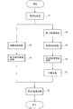
ここで従来の非同期置換型機能回路の設計方法について、図14及び図15を用いて具体的に説明する。 Here, a conventional method for designing an asynchronous replacement functional circuit will be described in detail with reference to FIGS.
図14は同期回路設計のフローチャートである。図14に示すように、従来の同期回路設計は、まず第1のステップ(図14におけるs1)として回路が表現されたRTL記述を用いて論理合成を行い、その後第2のステップ(図14におけるs2)として配置配線を行い、第3のステップ(図14におけるs3)としてタイミング検証を行い、第4のステップ(図14におけるs4)において、タイミング検証をパスした場合に設計完了となる。なお第2のステップにおける配置配線と第3のステップにおけるタイミング検証と、をまとめてレイアウト設計ともいう。また、設計完了とはマスク発注が可能な状態のことをいう。また、タイミング検証をパスできない場合は、第5のステップ(図14におけるs5)としてRTL記述作成段階へ戻り、適切な修正をする。以上が従来の同期回路設計である。 FIG. 14 is a flowchart of synchronous circuit design. As shown in FIG. 14, in the conventional synchronous circuit design, first, logic synthesis is performed using the RTL description in which the circuit is expressed as the first step (s1 in FIG. 14), and then the second step (in FIG. 14). The placement and routing is performed as s2), the timing verification is performed as the third step (s3 in FIG. 14), and the design is completed when the timing verification is passed in the fourth step (s4 in FIG. 14). The placement and routing in the second step and the timing verification in the third step are collectively referred to as layout design. Design completion means a state in which a mask can be ordered. If the timing verification cannot be passed, the process returns to the RTL description creation stage as a fifth step (s5 in FIG. 14), and appropriate correction is made. The above is the conventional synchronous circuit design.
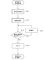
上記同期回路設計に対して、図15は特許文献1に記載の非同期置換型機能回路設計のフローチャートである。図15に示すように、特許文献1に記載の非同期置換型機能回路設計は、まず第1のステップ(図15におけるs0)として回路が表現されたRTL記述のうち、特定の単位回路を示す記述(同期式バイナリーカウンター回路を示す記述)を抽出し、抽出した特定の単位回路を示す記述を、対応する非同期回路の記述(非同期式バイナリーカウンター回路を示す記述)に自動的に置き換えることにより非同期置換型機能回路が表現されたRTL記述を作成する。その後、図14におけるフローチャートと同様に第2のステップ(図15におけるs1)として作成した非同期置換型機能回路が表現されたRTL記述を用いて論理合成を行い、第3のステップ(図15におけるs2)として配置配線を行い、第4のステップ(図15におけるs3)としてタイミング検証を行うことによりレイアウト設計をし、第5のステップ(図15におけるs4)においてタイミング検証をパスした場合に設計完了となる。また、タイミング検証をパスできない場合は、第6のステップ(図15におけるs5)としてRTL記述作成段階へ戻り、適切な修正がされる。以上が特許文献1に記載の非同期置換型機能回路設計である。 In contrast to the synchronous circuit design, FIG. 15 is a flowchart of the asynchronous replacement functional circuit design described in Patent Document 1. As shown in FIG. 15, the asynchronous replacement functional circuit design described in Patent Document 1 is a description showing a specific unit circuit in the RTL description in which the circuit is first expressed as the first step (s0 in FIG. 15). Asynchronous replacement by extracting (description showing synchronous binary counter circuit) and automatically replacing the extracted description showing specific unit circuit with the corresponding asynchronous circuit description (description showing asynchronous binary counter circuit) An RTL description in which a type function circuit is expressed is created. After that, as in the flowchart in FIG. 14, logic synthesis is performed using the RTL description expressing the asynchronous replacement functional circuit created as the second step (s1 in FIG. 15), and the third step (s2 in FIG. 15). ), The layout design is performed by performing timing verification as the fourth step (s3 in FIG. 15), and the design is completed when the timing verification is passed in the fifth step (s4 in FIG. 15). Become. If the timing verification cannot be passed, the process returns to the RTL description creation stage as the sixth step (s5 in FIG. 15), and appropriate correction is made. The above is the asynchronous replacement functional circuit design described in Patent Document 1.
上記に述べたとおり、非同期置換型機能回路の設計において、置換処理により生成されたRTL記述は、非同期回路の遅延の累積により、元のRTL記述に比べてレイアウト設計時にタイミング検証をパスできない可能性が高い。ただし、デバイスの特性や回路構成によっては、遅延が累積していってもレイアウト設計時のタイミング検証をパスする場合もあり、パスするか否かは論理合成時には判断できない。つまり、レイアウト設計まで設計工程が進んでからRTL記述作成段階へ戻って適切な修正をしなければならない可能性が従来の同期回路設計よりも高くなり、設計時間のロスに繋がるといった問題がある。設計時間のロスは、市場の動向などからくる設計に対する要求によって、間接的に設計の効率の低下、回路規模や消費電力の増大につながる恐れがある。 As described above, in the design of an asynchronous replacement functional circuit, there is a possibility that the RTL description generated by the replacement process cannot pass the timing verification at the time of layout design compared to the original RTL description due to the accumulated delay of the asynchronous circuit Is expensive. However, depending on the device characteristics and circuit configuration, timing verification at the time of layout design may be passed even if the delay is accumulated, and whether or not to pass cannot be determined at the time of logic synthesis. That is, there is a problem that the possibility of having to return to the RTL description creation stage and make an appropriate correction after the design process has progressed to layout design is higher than in conventional synchronous circuit design, leading to a loss of design time. The loss of design time may indirectly lead to a decrease in design efficiency, an increase in circuit scale, and power consumption, depending on the design requirements resulting from market trends.
上記問題を鑑み、本発明の一態様では、非同期置換型機能回路の設計において、設計時間のロスを抑えることで設計効率の低下を抑え、また回路規模が小さく、消費電力の少ない機能回路を設計することを課題の一つとする。 In view of the above problems, in one embodiment of the present invention, in designing an asynchronous replacement functional circuit, a design circuit is designed to suppress design time loss by suppressing design time loss, and to reduce the circuit scale and power consumption. One of the issues is to do.
本発明の一態様は、レジスタトランスファレベルで機能回路が表現された第1の記述のうち、同期の単位回路を示す第2の記述をブロック化し、ブロック化された第2の記述を一つの階層として、第1の記述を階層化された第3の記述に変換する階層化手段と、第3の記述の論理合成を行うことにより第1のネットリストを生成する第1の論理合成手段と、第1のネットリストをもとに配置配線を行う第1の配置配線手段と、ブロック化された第2の記述を非同期の単位回路を示す第4の記述に置換する第1の置換手段と、第4の記述の論理合成を行うことにより第2のネットリストを生成する第2の論理合成手段と、第2のネットリストをもとに配置配線を行う第2の配置配線手段と、第2の配置配線手段により配置配線が行われた非同期の単位回路の計算を行う計算手段と、計算手段での計算結果をもとに第1の配置配線手段により配置配線が行われた同期の単位回路を選択的に第2の配置配線手段により配置配線が行われた非同期の単位回路に置換する第2の置換手段と、を有する機能回路の設計システムである。 According to one aspect of the present invention, among the first descriptions in which the functional circuit is expressed at the register transfer level, the second description indicating the synchronization unit circuit is blocked, and the blocked second description is stored in one hierarchy. Hierarchizing means for converting the first description into a hierarchical third description; first logic synthesizing means for generating a first netlist by performing logic synthesis of the third description; First placement and routing means for performing placement and routing based on the first netlist; first replacement means for replacing the blocked second description with a fourth description indicating an asynchronous unit circuit; Second logic synthesis means for generating a second netlist by performing logic synthesis of the fourth description; second placement and routing means for performing placement and routing based on the second netlist; Asynchronous with place and route by place and route means A calculation means for calculating a unit circuit, and a synchronous unit circuit that has been placed and routed by the first placement and routing means based on the calculation result of the calculation means is selectively placed and routed by the second placement and routing means. And a second replacement unit that replaces the asynchronous unit circuit that has been performed.
また、本発明の一態様は、レジスタトランスファレベルで機能回路が表現された第1の記述のうち、同期の単位回路を示す第2の記述を抽出し、ブロック化することにより、ブロック化した第2の記述を一つの階層として、第1の記述を階層化した第3の記述に変換し、第3の記述の論理合成を行うことにより第1のネットリストを生成し、第1のネットリストをもとに第1の配置配線処理を行い、ブロック化した第2の記述を非同期の単位回路を示す第4の記述に置換し、第4の記述の論理合成処理を行うことにより第2のネットリストを生成し、第2のネットリストをもとに第2の配置配線処理を行い、第2の配置配線処理が行われた非同期の単位回路の計算処理を行い、計算処理での計算結果をもとに第1の配置配線処理が行われた同期の単位回路を選択的に第2の配置配線処理が行われた非同期の単位回路に置換する機能回路の設計方法である。 Further, according to one embodiment of the present invention, the second description indicating the synchronous unit circuit is extracted from the first description in which the functional circuit is expressed at the register transfer level, and the second description indicating the block is made into a block. The first description is converted into a third description in which the first description is hierarchized and the first description is converted into a third description, and a first netlist is generated by logical synthesis of the third description. The first placement and routing process is performed based on the second description, the second description in the block form is replaced with the fourth description indicating the asynchronous unit circuit, and the second description is performed by performing the logic synthesis process of the fourth description. Generate a netlist, perform the second placement and routing process based on the second netlist, perform the calculation process of the asynchronous unit circuit in which the second placement and routing process is performed, and the calculation result in the calculation process The first placement and routing process was performed based on Selectively the second place and route processing unit circuit of a design method of the functional circuit to replace the asynchronous unit circuits made.
なお、本発明の一態様において、同期の単位回路と非同期の単位回路はそれぞれ順序回路を有するカウンター回路とすることもできる。 Note that in one embodiment of the present invention, each of the synchronous unit circuit and the asynchronous unit circuit may be a counter circuit having a sequential circuit.
なお、本発明の一態様において、第1の配置配線処理により第1の配置配線処理で配置配線が行われた同期の単位回路のタイミング検証を行うこともできる。 Note that in one embodiment of the present invention, timing verification of a synchronous unit circuit in which placement and routing is performed in the first placement and routing process can be performed by the first placement and routing process.
また、本発明の一態様において、計算手段により第2の配置配線処理で配置配線が行われた非同期の単位回路のタイミング検証を行うこともできる。 In one embodiment of the present invention, timing verification of an asynchronous unit circuit in which placement and routing is performed in the second placement and routing process by the calculation unit may be performed.
本発明の一態様により、非同期置換型機能回路の設計において、配置配線後に同期回路のいずれかを自動的に非同期化することにより設計時間のロスを抑えることができ、設計効率の低下を抑えることができる。また本発明の一態様により回路規模が小さく、また消費電力の小さい非同期置換型機能回路を設計することができる。 According to one embodiment of the present invention, in designing an asynchronous replacement functional circuit, a loss of design time can be suppressed by automatically desynchronizing one of the synchronous circuits after placement and routing, thereby suppressing a decrease in design efficiency. Can do. Further, according to one embodiment of the present invention, an asynchronous replacement functional circuit with a small circuit scale and low power consumption can be designed.
(実施の形態1)
本実施の形態では、本発明の一態様である機能回路の設計システムについて説明する。
(Embodiment 1)
In this embodiment, a functional circuit design system which is one embodiment of the present invention will be described.
まず本実施の形態における機能回路の設計システムについて図1を用いて説明する。図1は、本実施の形態における機能回路の設計システムの構成を示すブロック図である。 First, a functional circuit design system according to the present embodiment will be described with reference to FIG. FIG. 1 is a block diagram showing a configuration of a functional circuit design system according to the present embodiment.
図1に示すように、本実施の形態における機能回路の設計システムは、階層化手段101と、第1の論理合成手段102と、第1の配置配線手段103と、第1の置換手段104と、第2の論理合成手段105と、第2の配置配線手段106と、計算手段107と、第2の置換手段108と、を有する。なお、それぞれの手段は、例えばプログラムにより構成することができる。
As shown in FIG. 1, the functional circuit design system according to the present embodiment includes a hierarchizing unit 101, a first logic synthesis unit 102, a first placement and routing unit 103, a
階層化手段101は、RTL記述109(第1の記述ともいう)のうち、同期の単位回路を示す記述(第2の記述ともいう)をブロック化し、ブロック化した第2の記述を一つの階層としてRTL記述109を階層化されたRTL記述(第3の記述ともいう)に変換する手段である。なお階層化とは、ある回路を示す記述が複数の階層からなる記述に変換されることをいう。具体的には、RTL記述109から指定回路情報110に相当する記述を検索し、指定回路情報110に相当するRTL記述をブロック化し、ブロック化された記述を一つの階層としてRTL記述109を階層化されたRTL記述に変換する。
The hierarchizing unit 101 blocks a description (also referred to as a second description) indicating a synchronization unit circuit from the RTL description 109 (also referred to as a first description), and converts the blocked second description into one hierarchy. The RTL description 109 is converted into a hierarchical RTL description (also referred to as a third description). Note that hierarchization means that a description indicating a certain circuit is converted into a description consisting of a plurality of hierarchies. Specifically, a description corresponding to the designated
なお、階層化されたRTL記述はRTL記述109と同一の回路機能を表現しており、さらに階層化されたRTL記述は、上位階層の記述と下位階層の記述に分類される。下位階層の記述はブロック化された第2の記述で構成され、上位階層の記述は下位階層の記述と、その他の回路を示す記述と、下位階層の記述とその他の回路を示す記述との接続関係の記述とで構成される。例えば図2に示すように、上位階層として機能回路201を示す記述がある場合、機能回路201を示す記述のうち、単位回路2021及び単位回路2022を示す記述がブロック化され、それぞれ回路ブロックとして表された単位回路2021及び単位回路2022を示す記述が下位階層の記述となる。なお、本実施の形態において上位階層の記述は、特に指定がなければ機能回路201を示す記述のことをいい、下位階層の記述は、特に指定がなければ単位回路2021及び単位回路2022を示す記述のことをいう。
The layered RTL description expresses the same circuit function as the RTL description 109, and the layered RTL description is classified into an upper layer description and a lower layer description. The description of the lower layer is composed of the second description that is blocked, and the description of the upper layer is the connection between the description of the lower layer, the description indicating the other circuit, and the description of the lower layer and the description indicating the other circuit. It consists of a description of the relationship. For example, as illustrated in FIG. 2, when there is a description indicating the
RTL記述109は、同期回路の設計手法に適したIEEE規格のRTL記述によって回路を表現した記述である。またRTL記述109で表現された回路は、全回路がグローバル・クロックによって駆動するものである。RTL記述109によって表現される回路としては、例えばCPU、画像処理回路、またはメモリなどがあり、これらの回路は一般的にカウンター回路やセレクター回路などの回路の集合体によって構成されている。本書類では、CPU、画像処理回路、またはメモリを示す記述は上位階層の記述であり、カウンター回路またはセレクター回路を示す記述は下位階層の記述である。 The RTL description 109 is a description expressing a circuit by an RTL description of the IEEE standard suitable for the design method of the synchronous circuit. The circuits expressed by the RTL description 109 are all driven by a global clock. As a circuit expressed by the RTL description 109, for example, there is a CPU, an image processing circuit, a memory, or the like, and these circuits are generally constituted by a collection of circuits such as a counter circuit and a selector circuit. In this document, a description indicating a CPU, an image processing circuit, or a memory is a description of an upper layer, and a description indicating a counter circuit or a selector circuit is a description of a lower layer.
指定回路情報110は、RTL記述109から抽出される記述によって示される特定の単位回路(例えば同期式カウンター回路)と同じ回路を示す情報である。なお、指定回路情報110は、階層化手段101を用いてRTL記述109から、指定された回路に該当する箇所を抽出するためのものであるため、指定回路情報110のフォーマットは階層化手段101に対応して設定されることが好ましい。例えば、階層化手段101において、RTL記述109における指定回路情報110の対応箇所をキーワードで検索する場合、指定回路情報110はキーワードにより特定の単位回路を表すというフォーマットになる。
The designated
第1の論理合成手段102は、階層化手段101により階層化されたRTL記述の論理合成を行い、ゲートレベルのネットリスト(第1のネットリストともいう)を生成する手段である。論理合成には、チップ面積若しくは遅延時間などの制約条件、または半導体製造技術のライブラリのセルなども用いられる。また、論理合成ツールとしては、例えばCadence Design Systems社製のBuild Gatesなどを用いることができる。 The first logic synthesis unit 102 is a unit that performs logic synthesis of the RTL description layered by the layering unit 101 and generates a gate-level netlist (also referred to as a first netlist). For logic synthesis, constraints such as chip area or delay time, or cells of a semiconductor manufacturing technology library are also used. As a logic synthesis tool, for example, Build Gates manufactured by Cadence Design Systems, Inc. can be used.
第1の配置配線手段103は、第1の論理合成手段102で生成されたネットリストをもとに配置配線を行い、ゲートレベルのネットリストを生成する手段である。なお、配置配線とは、ネットリストをもとに2次元平面上に回路の配置を行い、さらに2次元平面上で配線を行うことをいう。なお配置配線にはチップ面積、遅延時間などの制約条件や半導体製造技術のライブラリのセルなどを用いることがある。また、第1の配置配線手段103ではタイミング検証も併せて行われ、セットアップ時間やホールド時間などのタイミング情報が第2の置換手段108に出力される。タイミング検証は従来のタイミング検証だけではなく、例えば下位階層の記述に相当する単位回路を構成する回路の素子間に加え、下位階層の記述に相当する単位回路を1つの組み合わせ回路と見なしたタイミング検証も同時に行い、下位階層の記述に相当する単位回路の入出力端子のタイミング情報も第2の置換手段108に出力する。なお、下位階層の記述に相当する単位回路における入出力端子のタイミング情報とは、特に断りがない限りは、順序回路間の遅延情報及び、回路内に負荷されているゲート容量や配線に負荷される寄生容量などのことをいう。
The first placement and routing unit 103 is a unit that performs placement and routing based on the net list generated by the first logic synthesis unit 102 to generate a gate level net list. Note that the placement and wiring means that a circuit is placed on a two-dimensional plane based on a net list and further wired on a two-dimensional plane. For placement and routing, constraints such as chip area and delay time, and semiconductor manufacturing library cells may be used. The first placement and routing unit 103 also performs timing verification and outputs timing information such as setup time and hold time to the
第1の置換手段104は、階層化手段101で階層化された第2の記述を非同期の単位回路を示す記述(第4の記述ともいう)に置換する手段である。なお、第2の記述と第4の記述とは同期回路であるか非同期回路であるかが異なるだけであって表現された回路機能は同一である。 The first replacement means 104 is means for replacing the second description hierarchized by the hierarchization means 101 with a description (also referred to as a fourth description) indicating an asynchronous unit circuit. The second description and the fourth description differ only in whether they are synchronous circuits or asynchronous circuits, and the expressed circuit functions are the same.
第2の論理合成手段105は、第4の記述の論理合成を行い、ゲートレベルのネットリスト(第2のネットリストともいう)を生成する手段である。論理合成には、チップ面積遅延時間などの制約条件、または半導体製造技術のライブラリのセルなども用いられる。論理合成ツールとしては、例えばCadence Design Systems社製のBuild Gatesなどを用いることができる。 The second logic synthesis unit 105 is a unit that performs logic synthesis of the fourth description and generates a gate level netlist (also referred to as a second netlist). For logic synthesis, constraints such as chip area delay time or library cells of semiconductor manufacturing technology are also used. As the logic synthesis tool, for example, Build Gates manufactured by Cadence Design Systems can be used.
第2の配置配線手段106は、第2の論理合成手段105により生成されたネットリストをもとに配置配線を行う手段である。なお配置配線には、チップ面積及び遅延時間などの制約条件や半導体製造技術のライブラリのセルなども用いることがある。また、第2の配置配線手段106では、配線接続情報やゲート容量や配線に負荷される寄生容量などの回路情報が生成され、計算手段107に出力される。
The second placement and routing means 106 is a means for performing placement and routing based on the net list generated by the second logic synthesis means 105. For placement and routing, constraints such as chip area and delay time, and semiconductor manufacturing library cells may be used. In the second placement and routing unit 106, circuit information such as wiring connection information, gate capacitance, and parasitic capacitance loaded on the wiring is generated and output to the
計算手段107は、シミュレーション手段ともいい、第2の配置配線手段106から入力された配線接続情報やゲート容量や配線に負荷される寄生容量などの回路情報と第2の配置配線手段106から入力されたネットリストを用いてspiceなどの回路シミュレーターで計算(シミュレーションともいう)を行う手段である。その際の計算条件として、例えば入力信号の組み合わせ、入力信号の立ち上がりまたは立ち下がりの傾き、又は出力端の負荷容量を変えて計算を行う。例えば、入力信号の値の組み合わせを4条件、入力信号の立ち上がりまたは立ち下がりの傾きを5条件、出力端の負荷容量を5条件としたとき、計算は4×5×5、すなわち100回行う。この計算により、入力されたネットリストに対する遅延情報が得られ、その結果をデータテーブルとしてファイルに出力する。また、計算手段107では第2の配置配線手段106で行わなかったタイミング検証の代わりにタイミング検証が行われる。タイミング検証とは、動的タイミング検証と静的タイミング検証とに大きく分けられる。 The calculating means 107 is also called a simulation means, and is inputted from the second placement and routing means 106 and circuit information such as wiring connection information inputted from the second placement and routing means 106, gate capacitance and parasitic capacitance loaded on the wiring. This is means for performing calculation (also called simulation) using a circuit simulator such as spice using the netlist. As calculation conditions at that time, for example, the calculation is performed by changing the combination of input signals, the rising or falling slope of the input signals, or the load capacity of the output terminal. For example, when the input signal value combination is 4 conditions, the rising or falling slope of the input signal is 5 conditions, and the load capacitance at the output end is 5 conditions, the calculation is performed 4 × 5 × 5, that is, 100 times. By this calculation, delay information for the input netlist is obtained, and the result is output as a data table to a file. Further, the calculation means 107 performs timing verification instead of the timing verification not performed by the second placement and routing means 106. Timing verification is roughly divided into dynamic timing verification and static timing verification.
ここで動的タイミング検証と静的タイミング検証の違いについて説明する。動的タイミング検証とは、実際に回路にテストパターンを入力して計算し、その出力状況から回路の動作に異常がないかを確認し、異常がある場合は、適切な動作になるように修正する検証である。 Here, the difference between dynamic timing verification and static timing verification will be described. With dynamic timing verification, a test pattern is actually input to the circuit and calculated, and it is checked whether there is an abnormality in the operation of the circuit based on the output status. It is verification to do.
一方、静的タイミング検証とは、配線接続情報やゲート容量や配線に負荷される寄生容量などの回路情報のみから基準となるクロック信号とデータの遅延関係に異常がないかを確認し、異常がある場合は、適切な遅延関係になるように修正する検証である。なお、本明細書中に記載されているタイミング検証とは、特に断りがなければ、静的タイミング検証のことを指す。同期回路の場合は、順序回路間のクリティカルパスの遅延値を計算して、その遅延値と基準となるクロック信号のタイミング(例えば、クロック信号の周期やクロック信号の遅延などを基にした時間)により検証が可能であるので、静的タイミング検証が可能である。しかしながら、非同期回路の場合は基準となるクロック信号が全ての順序回路に供給されていない場合があるので、順序回路間のクリティカルパスの遅延値を計算して、その遅延値と基準となるクロック信号のタイミングにより検証はできない。したがって、非同期回路には動的なタイミング検証が必要となり、計算手段107では、タイミング検証として動的タイミング検証が行われる。なお、計算手段107の一部として市販のセルキャラクタライズツールが用いられる。セルキャラクタライズツールとしては、例えばSILVACO社製のAccuCellなどを用いることができる。 Static timing verification, on the other hand, confirms that there is no abnormality in the delay relationship between the reference clock signal and data based only on circuit information such as wiring connection information, gate capacitance, and parasitic capacitance loaded on the wiring. In some cases, the verification is corrected so as to obtain an appropriate delay relationship. Note that the timing verification described in this specification refers to static timing verification unless otherwise specified. In the case of a synchronous circuit, the delay value of the critical path between sequential circuits is calculated, and the delay value and the timing of the reference clock signal (for example, the time based on the period of the clock signal, the delay of the clock signal, etc.) Therefore, static timing verification is possible. However, in the case of an asynchronous circuit, the reference clock signal may not be supplied to all the sequential circuits. Therefore, the delay value of the critical path between the sequential circuits is calculated, and the delay value and the reference clock signal are calculated. It cannot be verified depending on the timing. Therefore, dynamic timing verification is required for the asynchronous circuit, and the calculation means 107 performs dynamic timing verification as timing verification. A commercially available cell characterization tool is used as part of the calculation means 107. As a cell characterization tool, for example, AccuCell manufactured by SILVACO can be used.
第2の置換手段108は、計算手段107での計算結果をもとに第1の配置配線手段103で配置された回路の一部、例えば下位階層の単位回路のいずれかを選択的に第2の配置配線手段106で配置された回路に置換する手段である。さらに、第2の置換手段108では、置換が完了したレイアウトで再度タイミング検証が行われる。 The second replacement means 108 selectively selects a part of the circuit arranged by the first placement and routing means 103 based on the calculation result of the calculation means 107, for example, one of lower unit circuits. This means replaces the circuit disposed by the placement and routing means 106. Further, the second replacement means 108 performs the timing verification again with the layout in which the replacement has been completed.
次に上記設計システムによる機能回路の設計方法について図3を用いて説明する。図3は、本実施の形態における設計システムによる設計方法を示すフローチャートである。 Next, a functional circuit design method by the design system will be described with reference to FIG. FIG. 3 is a flowchart showing a design method by the design system in the present embodiment.
図3に示すように、まず第1のステップ(図3におけるS1)として階層化手段101により階層化処理が行われる。階層化処理では、RTL記述109のうち、指定回路情報110に記載された特定の単位回路に相当する記述がブロック化され、ブロック化された記述を一つの階層として、RTL記述109が階層化されたRTL記述に変換される。
As shown in FIG. 3, the hierarchizing means 101 first performs a hierarchizing process as a first step (S1 in FIG. 3). In the hierarchization processing, a description corresponding to a specific unit circuit described in the designated
階層化処理後、階層化されたRTL記述を用いた処理と、下位階層の記述であるブロック化された単位回路を示す記述を用いた処理との2通りの処理が行われる。それぞれの処理について以下に説明する。 After the hierarchization process, two types of processes are performed: a process using a hierarchized RTL description and a process using a description indicating a block unit circuit which is a description of a lower hierarchy. Each process will be described below.
階層化されたRTL記述を用いた処理については、階層化処理の次に第2のステップ(図3におけるS2)として、第1の論理合成手段102により論理合成処理が行われる。論理合成処理について図4を用いて具体的に説明する。 As for the process using the hierarchized RTL description, the logic synthesis process is performed by the first logic synthesis unit 102 as the second step (S2 in FIG. 3) after the hierarchy process. The logic synthesis process will be specifically described with reference to FIG.
図4に示すように、まずステップ1(図4におけるS2−1)として論理回路が生成される。ここでは入力されたRTL記述109から、ステートマシンの状態コードの割り当て、フリップフロップの割り付け、及び組み合わせ論理の生成などが行われることによりゲートレベルの論理回路が生成される。 As shown in FIG. 4, first, a logic circuit is generated as step 1 (S2-1 in FIG. 4). Here, a logic circuit at the gate level is generated from the input RTL description 109 by performing state machine state code assignment, flip-flop assignment, combinational logic generation, and the like.
次にステップ2(図4におけるS2−2)として半導体製造プロセスに依存しない範囲で論理の最適化が行われる。具体的には指定した制約条件を満たすように論理ゲート数(チップ面積)と論理段数(遅延時間)などが調整される。例えば、a+a×b=aのようなブール代数の性質を用いた冗長論理の削除、f=(a+b)×(c+d)のような論理をf=a×c+a×d+b×c+b×dのように展開する論理の展開、またはf=a×c+a×d+b×c+b×dのような論理をf=(a+b)×(c+d)のようにする論理の多段化などが行われる。なお、a、b、c、d、及びfはそれぞれ集合を表す。 Next, in step 2 (S2-2 in FIG. 4), logic optimization is performed within a range that does not depend on the semiconductor manufacturing process. Specifically, the number of logic gates (chip area) and the number of logic stages (delay time) are adjusted so as to satisfy the specified constraint conditions. For example, deletion of redundant logic using Boolean algebraic properties such as a + a × b = a, and logic such as f = (a + b) × (c + d) as f = a × c + a × d + b × c + b × d The logic to be developed is expanded or the logic such as f = a * c + a * d + b * c + b * d is made multi-stage such as f = (a + b) * (c + d). Note that a, b, c, d, and f each represent a set.
さらにステップ3(図4におけるS2−3)として全体の論理機能を変えることなく論理の再構成が必要か否か判断される。論理の再構成とは、機能は同じだが構成の異なる論理へ置き換えることをいい、基準となるクロック信号とデータの遅延関係を表すパラメータを所定の値に収束させるためや、回路規模縮小のために行われる。必要であると判断された場合には、ステップ5(図4におけるS2−5)として論理の再構成が行われる。 Further, in step 3 (S2-3 in FIG. 4), it is determined whether or not logic reconfiguration is necessary without changing the overall logic function. Logic reconfiguration refers to replacement with logic that has the same function but different configuration, in order to converge the parameters representing the delay relationship between the reference clock signal and data to a predetermined value, or to reduce the circuit scale Done. If it is determined that it is necessary, the logic is reconfigured as step 5 (S2-5 in FIG. 4).
最後に、ステップ4(図4におけるS2−4)として準備した半導体製造技術のライブラリのセルへのマッピングが行われる。すなわち、論理(ゲート)や順序回路が、準備した半導体製造技術のライブラリのマクロセルに置き換わる。以上の工程をもってゲートレベルのネットリストが生成される。なお、論理合成処理において階層化手段101により階層化されたRTL記述は階層を有したまま保持される。以上が論理合成処理である。 Finally, mapping to the cell of the library of the semiconductor manufacturing technology prepared as step 4 (S2-4 in FIG. 4) is performed. That is, the logic (gate) and the sequential circuit are replaced with the prepared macro cell of the library of the semiconductor manufacturing technology. The gate level netlist is generated through the above steps. Note that the RTL description hierarchized by the hierarchizing means 101 in the logic synthesis process is held with a hierarchy. The above is the logic synthesis process.
次に第3のステップ(図3におけるS3)として、第1の配置配線手段103により第1の配置配線処理が行われる。第1の配置配線処理について図5を用いて具体的に説明する。図5は本実施の形態における第1の配線処理を示すフローチャート図である。 Next, as a third step (S3 in FIG. 3), the first placement and routing unit 103 performs a first placement and routing process. The first placement and routing process will be specifically described with reference to FIG. FIG. 5 is a flowchart showing the first wiring process in the present embodiment.
図5に示すように、まずステップ1(図5におけるS3−1)として第1の論理合成手段102により生成されたゲートレベルのネットリスト、並びにチップ面積及び遅延時間などの制約条件や半導体製造技術のライブラリのセルなどを用いてレイアウトが作成され、ゲートレベルのネットリストが生成される。 As shown in FIG. 5, first, as a step 1 (S3-1 in FIG. 5), a gate-level netlist generated by the first logic synthesis means 102, constraints such as chip area and delay time, and semiconductor manufacturing technology A layout is created using the cells of the library of, and a gate level netlist is generated.
次にステップ2(図5におけるS3−2)として、配線接続情報やゲート容量や配線に負荷される寄生容量などの回路データが第2の置換手段108に出力される。
Next, in step 2 (S3-2 in FIG. 5), circuit data such as wiring connection information, gate capacitance, and parasitic capacitance loaded on the wiring is output to the
次にステップ3(図5におけるS3−3)としてタイミング検証が行われ、ステップ4(図5におけるS3−4)として機能回路を構成するそれぞれの回路のセットアップ時間やホールド時間などのタイミング情報が第2の置換手段108に出力される。なお、第1の配置配線処理におけるタイミング検証は、従来のタイミング検証だけではなく、例えば下位階層の記述に相当する単位回路を構成する順序回路の素子間に加え、単位回路を1つの組み合わせ回路と見なしたタイミング検証も同時に行われ、単位回路における入出力端子のタイミング情報も第2の置換手段108に出力される。なお、タイミング情報は以下のように出力される。
Next, timing verification is performed as step 3 (S3-3 in FIG. 5), and timing information such as setup time and hold time of each circuit constituting the functional circuit is obtained as step 4 (S3-4 in FIG. 5). Is output to the second replacement means 108. Note that the timing verification in the first placement and routing process is not limited to the conventional timing verification. For example, the unit circuit is combined with one combinational circuit in addition to the elements of the sequential circuit constituting the unit circuit corresponding to the description of the lower hierarchy. The considered timing verification is also performed at the same time, and the timing information of the input / output terminals in the unit circuit is also output to the
まず生成されたネットリストを用いて各素子(論理ゲートまたはトランジスタ)の遅延時間情報と配線遅延時間情報をもとに対象回路に相当するグラフが作成される。そして、このグラフから最大遅延時間のパスや最小遅延時間のパスなどが抽出され、併せて当該パスの最大遅延時間や最小遅延時間からタイミング情報が生成される。ここでのグラフとはグラフ理論のグラフをいい、各素子(論理ゲートまたはトランジスタ)のつながり方に着目して抽象化された点とそれを結ぶ線を概念化したものをいう。 First, a graph corresponding to the target circuit is created based on the delay time information of each element (logic gate or transistor) and the wiring delay time information using the generated netlist. Then, a path with the maximum delay time, a path with the minimum delay time, and the like are extracted from the graph, and timing information is generated from the maximum delay time and the minimum delay time of the path. The graph here refers to a graph of graph theory, which is a conceptualization of points abstracted by focusing on how elements (logic gates or transistors) are connected and lines connecting them.
以上が第1の配置配線処理である。なお、第1の配置配線処理において、階層化手段による階層化は維持される。また、下位階層の単位回路内の素子同士は、できるだけ近い位置に配置されることが好ましい。 The above is the first placement and routing process. Note that hierarchization by the hierarchizing means is maintained in the first placement and routing process. Moreover, it is preferable that the elements in the unit circuits in the lower hierarchy are arranged as close as possible.
一方、階層化されたRTL記述のうち、下位階層の記述であるブロック化された単位回路を示す記述を用いる処理については、階層化処理の次に第2のステップ(図3におけるS4)として第1の置換処理が行われる。第1の置換処理について以下に説明する。 On the other hand, for the processing using the description indicating the block unit circuit which is the description of the lower layer among the layered RTL descriptions, the second step (S4 in FIG. 3) is the second step after the layering processing. 1 replacement processing is performed. The first replacement process will be described below.
第1の置換処理では、ブロック化された単位回路を示す記述が、別途作成された非同期の単位回路を示す記述に置換される。このとき別途作成された非同期の単位回路を示す記述と、置換されるブロック化された単位回路を示す記述は同一機能を表す。なお、非同期の単位回路を示す記述は、第1の置換処理時に作成することもでき、また階層化処理の際に用いられる指定回路情報110に予め記載しておき、第1の置換処理時に用いることもできる。以上が第1の置換処理である。
In the first replacement process, a description indicating a block unit circuit is replaced with a description indicating an asynchronous unit circuit created separately. At this time, the description indicating the asynchronous unit circuit created separately and the description indicating the block unit circuit to be replaced represent the same function. The description indicating the asynchronous unit circuit can be created at the time of the first replacement process, and is described in advance in the
次に第3のステップ(図3におけるS5)として第2の論理合成手段105により非同期の単位回路を示す記述の論理合成処理が行われ、ゲートレベルのネットリストが生成される。論理合成処理の具体的な説明については、上記第2のステップS2における論理合成処理と同じであるため、第2のステップS2における論理合成処理の説明を援用する。 Next, as a third step (S5 in FIG. 3), the second logic synthesis unit 105 performs a logic synthesis process for describing the asynchronous unit circuit to generate a gate level netlist. Since the specific description of the logic synthesis process is the same as the logic synthesis process in the second step S2, the description of the logic synthesis process in the second step S2 is cited.
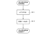
次に第4のステップ(図3におけるS6)として第2の配置配線手段106により第2の配置配線処理が行われる。第2の配置配線処理について図6を用いて具体的に説明する。図6は、本実施の形態における第2の配置配線処理を示すフローチャートである。 Next, a second placement and routing process is performed by the second placement and routing means 106 as a fourth step (S6 in FIG. 3). The second placement and routing process will be specifically described with reference to FIG. FIG. 6 is a flowchart showing the second placement and routing process in the present embodiment.
図6に示すように、まずステップ1(図6におけるS6−1)として第2の論理合成手段105により生成されたネットリスト、チップ面積、遅延時間などの制約条件、及び半導体製造技術のライブラリのセルなどを用いてレイアウトが作成され、ゲートレベルのネットリストが生成される。 As shown in FIG. 6, first, as a step 1 (S6-1 in FIG. 6), constraints such as a net list, chip area, delay time, etc. generated by the second logic synthesis means 105, and a library of semiconductor manufacturing technology A layout is created using cells or the like, and a gate-level netlist is generated.
次にステップ2(図6におけるS6−2)として、配線接続情報やゲート容量や配線に負荷される寄生容量などの回路データが計算手段107に出力される。以上が第2の配置配線処理である。 Next, as step 2 (S6-2 in FIG. 6), circuit data such as wiring connection information, gate capacitance, and parasitic capacitance loaded on the wiring is output to the calculation means 107. The above is the second placement and routing process.
次に第5のステップ(図3におけるS7)として、計算手段107により計算処理が行われる。計算処理では、第2の配置配線手段106から入力された配線接続情報やゲート容量や配線に負荷される寄生容量などの回路情報と第2の配置配線手段106から入力されたネットリストを使用して計算が行われる。この計算により、入力されたネットリストに対する遅延情報が得られ、その結果がデータテーブルとしてファイルに出力される。さらに計算手段107ではタイミング検証が行われる。 Next, as a fifth step (S7 in FIG. 3), calculation processing is performed by the calculation means 107. In the calculation process, the wiring information input from the second placement and routing unit 106, circuit information such as gate capacitance and parasitic capacitance loaded on the wiring, and the net list input from the second placement and routing unit 106 are used. The calculation is performed. By this calculation, delay information for the input netlist is obtained, and the result is output to a file as a data table. Further, the calculation means 107 performs timing verification.
第1の配置配線処理及び計算処理が終了したら次のステップ(図3におけるS8)として第2の置換手段108により第2の置換処理が行われる。第2の置換処理について図7を用いて具体的に説明する。図7は本実施の形態における第2の置換手段を示すフローチャートである。
When the first placement and routing process and the calculation process are completed, the
図7に示すように、まずステップ1(図7におけるS8−1)として、計算手段107で得られた出力遅延情報と、第1の配置配線手段103から入力された下位階層の単位回路の入出力端子のタイミング情報をもとに第1の配置配線手段103で配置された下位階層の記述に対応する回路いずれかが選択的に第2の配置配線手段106で配置された非同期の単位回路を示す記述に対応する回路にレイアウト上で置換される。 As shown in FIG. 7, first, as Step 1 (S8-1 in FIG. 7), the output delay information obtained by the calculation means 107 and the input of the lower layer unit circuit inputted from the first placement and routing means 103 are input. Based on the timing information of the output terminal, an asynchronous unit circuit in which any one of the circuits corresponding to the description of the lower hierarchy arranged by the first arrangement / wiring means 103 is selectively arranged by the second arrangement / wiring means 106 is selected. A circuit corresponding to the description shown is replaced on the layout.
次にステップ2(図7におけるS8−2)として置換が完了したレイアウトで再度タイミング検証を行う。さらにステップ3(図7におけるS8−3)としてセットアップ時間やホールド時間などが所望のタイミング仕様に合致しているかどうかを調べ、合致しているようなら設計完了となる。なお、タイミング仕様は、タイミング検証の合否判定に使われる値になる。また、合致していない場合は、ステップ4(図7におけるS8−4)として適切に修正される。以上が第2の置換処理である。 Next, in step 2 (S8-2 in FIG. 7), the timing verification is performed again with the layout in which the replacement has been completed. Further, in step 3 (S8-3 in FIG. 7), it is checked whether the setup time, hold time, and the like match the desired timing specifications. If they match, the design is completed. Note that the timing specification is a value used for the pass / fail judgment of the timing verification. On the other hand, if they do not match, it is appropriately corrected as step 4 (S8-4 in FIG. 7). The above is the second replacement process.
上記のように、本発明の一態様である機能回路の設計システムでは、配置配線後に選択的に同期回路が自動的に非同期化されるため、タイミング検証をパスできない場合でも修正が容易であり、設計時間のロスを抑え、設計効率の低下を抑えることができる。また、同期回路を選択的に非同期化するという簡易な方法で回路規模が小さく、また消費電力の小さい機能回路を設計することができる。 As described above, in the functional circuit design system according to one aspect of the present invention, the synchronization circuit is automatically desynchronized after placement and routing, so that even if timing verification cannot be passed, correction is easy. Loss of design time can be suppressed and a decrease in design efficiency can be suppressed. Further, it is possible to design a functional circuit with a small circuit scale and low power consumption by a simple method of selectively desynchronizing the synchronous circuit.
(実施の形態2)
本実施の形態では、本発明の一態様である機能回路の設計システムまたは機能回路の設計方法により設計可能な回路を備えたデバイスの例として、半導体装置について説明する。
(Embodiment 2)
In this embodiment, a semiconductor device is described as an example of a device including a circuit that can be designed by the functional circuit design system or the functional circuit design method which is one embodiment of the present invention.
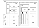
本実施の形態における半導体装置の構成について図8を用いて説明する。図8は、本実施の形態における半導体装置の構成を示すブロック図である。 A structure of the semiconductor device in this embodiment will be described with reference to FIGS. FIG. 8 is a block diagram showing a configuration of the semiconductor device in this embodiment.
図8に示すように、半導体装置500は、RF回路501、クロック信号生成回路502、ロジック回路503、及びアンテナ部518におけるアンテナ517により構成されている。なお、図8には示していないが、半導体装置500は、無線通信装置(リーダライタ、または質問器など、無線により通信が可能なもの)などの外部の回路とアンテナ517を介して無線信号の送受信を行っている。なお、データの伝送形式は、一対のコイルを対向配置して相互誘導によって交信を行う電磁結合方式、誘導電磁界によって交信する電磁誘導方式、電波を利用して交信する電波方式の3つに大別され、本実施の形態ではいずれの方式でも適用することができる。
As illustrated in FIG. 8, the
次に各回路の構成について説明する。RF回路501は電源回路504と、復調回路505と、変調回路506と、を有する。また、クロック信号生成回路502は、分周回路507と、カウンター回路509と、基準クロック信号生成回路519と、を有する。また、ロジック回路503は、演算処理を行う機能を有し、コントローラ513と、CPU(中央演算回路ともいう)510と、ROM(Read Only Memory)511と、RAM(Random Access Memory)512と、を有する。
Next, the configuration of each circuit will be described. The
また、コントローラ513は、CPUインターフェース514と、RFインターフェース515と、メモリコントローラ516と、を有する。
The
また、RF回路501において、電源回路504は、整流回路と、保持容量と、を有し、受信した信号から電源電圧を生成し、その他の回路に供給する機能を有する。また復調回路505は、整流回路と、LPF(ローパスフィルタ)と、を有し、通信信号からコマンドやデータを抽出する機能を有する。変調回路506は、送信データを変調する機能を有し、変調されたデータは、アンテナ517から送信信号として送信される。
In the
次に本実施の形態における半導体装置の動作について説明する。まず、外部の通信装置から送信された信号が半導体装置で受信される。半導体装置に入力された受信信号は、復調回路505で復調された後、コントローラ513におけるRFインターフェース515に出力される。RFインターフェース515に入力された受信信号は、CPUインターフェース514を介してCPU510で演算処理される。また、RFインターフェース515に入力された受信信号により、メモリコントローラ516を介してROM511、RAM512に対するアクセスが行われる。
Next, operation of the semiconductor device in this embodiment is described. First, a signal transmitted from an external communication device is received by a semiconductor device. The received signal input to the semiconductor device is demodulated by the
そして、CPU510による演算処理、ROM511、RAM512におけるデータの入出力後に送信データが生成され、送信データは、信号として変調回路506で変調され、アンテナ517から外部の通信装置に送信される。
Transmission data is generated after arithmetic processing by the
本発明の一態様である機能回路の設計システムまたは機能回路の設計方法は、上記半導体装置のロジック回路などの設計に好適である。本発明の一態様である機能回路の設計システムまたは機能回路の設計方法を用いることにより回路規模が小さく、消費電力の低いロジック回路を設計することができる。 A functional circuit design system or a functional circuit design method according to one embodiment of the present invention is suitable for designing a logic circuit of the semiconductor device. By using the functional circuit design system or the functional circuit design method which is one embodiment of the present invention, a logic circuit with a small circuit scale and low power consumption can be designed.
さらに上記半導体装置は、様々な用途で使用される。上記半導体装置の使用例について図9を用いて説明する。図9は半導体装置の使用例を示す模式図である。 Further, the semiconductor device is used for various purposes. An example of use of the semiconductor device will be described with reference to FIGS. FIG. 9 is a schematic view showing an example of use of a semiconductor device.
図9に示すように、半導体装置の用途は広範囲にわたるが、例えば、紙幣、硬貨、有価証券類、無記名債券類、証書類(運転免許証や住民票など、図9(A)参照)、包装用容器類(包装紙やボトルなど、図9(C)参照)、記録媒体(DVDソフトやビデオテープなど、図9(B)参照)、乗り物類(自転車など、図9(D)参照)、身の回り品(鞄や眼鏡など)、食品類、植物類、動物類、人体、衣類、生活用品類、または電子機器(液晶表示装置、EL表示装置、テレビジョン装置、または携帯電話)などの物品、若しくは各物品に取り付ける荷札(図9(E)、図9(F)参照)などに設けて使用することができる。 As shown in FIG. 9, semiconductor devices have a wide range of uses. For example, banknotes, coins, securities, bearer bonds, certificates (driver's license, resident's card, etc., see FIG. 9A), packaging Containers (such as wrapping paper and bottles, see FIG. 9C), recording media (DVD software and video tapes, see FIG. 9B), vehicles (such as bicycles, see FIG. 9D), Items such as personal items (such as bags and glasses), foods, plants, animals, human bodies, clothing, daily necessities, or electronic devices (liquid crystal display devices, EL display devices, television devices, or mobile phones), Alternatively, it can be used by being provided on a tag (see FIGS. 9E and 9F) attached to each article.
半導体装置600は、プリント基板に実装、表面に貼る、または埋め込むことにより、物品に固定される。例えば、本であれば紙に埋め込む、または有機樹脂からなるパッケージであれば当該有機樹脂に埋め込み、各物品に固定される。半導体装置600は、小型、薄型、軽量を実現するため、物品に固定した後もその物品自体のデザイン性を損なうことがない。また、紙幣、硬貨、有価証券類、無記名債券類、または証書類などに半導体装置600を設けることにより、認証機能を設けることができ、この認証機能を活用すれば、偽造を防止することができる。また、包装用容器類、記録媒体、身の回り品、食品類、衣類、生活用品類、または電子機器などに半導体装置を取り付けることにより、検品システムなどのシステムの効率化を図ることができる。また、乗り物類であっても、半導体装置を取り付けることにより、盗難などに対するセキュリティ性を高めることができる。
The
以上のように、本発明の一態様により設計した回路を備えた半導体装置は、消費電力を少なくでき、また回路面積を小さくできるため、上記のような硬貨などの小型のものから、電子機器などの大型のものまで、大きさに限定されずに各用途に用いることができる。また、各用途に用いることにより、情報のやりとりに用いられるデータを正確の値のまま維持することができるため、物品の認証性、またはセキュリティ性の信頼性を高めることができる。 As described above, since a semiconductor device including a circuit designed according to one embodiment of the present invention can reduce power consumption and circuit area, the electronic device can be used from a small one such as a coin as described above. Can be used in various applications without being limited to a size. Moreover, since the data used for exchanging information can be maintained at an accurate value by being used for each application, the authenticity of the article or the reliability of the security can be improved.
なお、本実施の形態は、他の実施の形態と適宜組み合わせることができる。 Note that this embodiment can be combined with any of the other embodiments as appropriate.
(実施の形態3)
本実施の形態では、本発明の一態様である機能回路の設計システムまたは機能回路の設計方法により設計可能な回路を備えたデバイスの一例として、表示装置について説明する。
(Embodiment 3)
In this embodiment, a display device is described as an example of a device including a circuit that can be designed by a functional circuit design system or a functional circuit design method which is one embodiment of the present invention.
まず本実施の形態における表示装置の構成について図10を用いて説明する。図10は、本実施の形態における表示装置の構成を示すブロック図である。 First, the structure of the display device in this embodiment is described with reference to FIG. FIG. 10 is a block diagram illustrating a configuration of the display device in this embodiment.
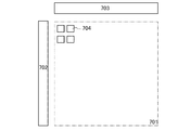
図10に示すように、本実施の形態における表示装置は、画素部701と、走査線駆動回路702と、信号線駆動回路703と、を有する。
As illustrated in FIG. 10, the display device in this embodiment includes a pixel portion 701, a scan
画素部701は、複数の画素704を有し、複数の画素704が行列方向に複数存在する、いわゆるドットマトリクス構造である。それぞれの画素は走査線(図示せず)を介して走査線駆動回路702に電気的に接続され、信号線(図示せず)を介して信号線駆動回路703に電気的に接続される。
The pixel portion 701 has a plurality of
走査線駆動回路702は、データを書き込む画素704を選択する回路であり、走査線を介して選択信号を画素に出力する。
The scan
信号線駆動回路703は、画素704に書き込むデータを信号として出力する回路であり、信号線を介して走査線駆動回路702により選択された画素704にデータ信号を出力する。
The signal
次に本実施の形態における表示装置の走査線駆動回路及び信号線駆動回路の構成の一例について説明する。 Next, an example of a structure of the scan line driver circuit and the signal line driver circuit of the display device in this embodiment is described.
まず走査線駆動回路の構成の一例について図11(A)を用いて説明する。図11(A)は、本実施の形態のおける表示装置の走査線駆動回路の構成の一例を示すブロック図である。 First, an example of a structure of the scan line driver circuit is described with reference to FIG. FIG. 11A is a block diagram illustrating an example of a structure of a scan line driver circuit in the display device in this embodiment.
図11(A)に示すように図10における走査線駆動回路702は、シフトレジスタ800、レベルシフタ801、バッファ802と、を有する。
As shown in FIG. 11A, the scan
シフトレジスタ800にはゲートスタートパルス(GSP)、ゲートクロック信号(GCK)などの信号が入力される。
Signals such as a gate start pulse (GSP) and a gate clock signal (GCK) are input to the
次に信号線駆動回路の構成の一例について図11(B)を用いて説明する。図11(B)は本実施の形態における表示装置の信号線駆動回路の構成の一例を示す断面図である。 Next, an example of a structure of the signal line driver circuit is described with reference to FIG. FIG. 11B is a cross-sectional view illustrating an example of a structure of the signal line driver circuit of the display device in this embodiment.
図11(B)に示すように図10における信号線駆動回路703は、シフトレジスタ803、第1のラッチ回路804、第2のラッチ回路805、レベルシフタ806、バッファ807と、を有する。
As shown in FIG. 11B, the signal
バッファ807は、信号を増幅させる機能を有し、オペアンプなどを有する。シフトレジスタ803には、スタートパルス(SSP)などの信号が入力され、第1のラッチ回路804にはビデオ信号などのデータ(DATA)が入力される。第2のラッチ回路805にはラッチ(LAT)信号を一時保持することができ、保持されたラッチ信号を一斉に図10における画素部701に出力させる。これを線順次駆動と呼ぶ。そのため、線順次駆動ではなく、点順次駆動を行う画素であれば、第2のラッチ回路805は不要とすることができる。
The
本発明の一態様は、上記シフトレジスタ800などの設計に好適である。本発明の一態様を用いることにより設計が容易になる。
One embodiment of the present invention is suitable for designing the
また、上記表示装置は様々な電子機器の表示部に用いることができる。上記表示装置を搭載した電子機器の具体例について図12を用いて説明する。図12は、本実施の形態における電子機器の構成を示す図である。 The display device can be used for display portions of various electronic devices. A specific example of an electronic device equipped with the display device will be described with reference to FIGS. FIG. 12 is a diagram illustrating a configuration of the electronic device in this embodiment.
図12(A)はディスプレイ装置であり、筐体901、支持台902、表示部903、スピーカー部904、ビデオ入力端子905などを含む。上記表示装置は、表示部903に用いることができる。なお、ディスプレイ装置は、パーソナルコンピュータ用、TV放送受信用、広告表示用などの全てのディスプレイ装置が含まれる。
FIG. 12A illustrates a display device, which includes a
図12(B)はデジタルスチルカメラであり、本体911、表示部912、受像部913、操作キー914、外部接続ポート915、シャッターボタン916などを含む。上記表示装置は、表示部912に用いることができる。
FIG. 12B illustrates a digital still camera, which includes a
図12(C)はノート型パーソナルコンピュータであり、本体921、筐体922、表示部923、キーボード924、外部接続ポート925、ポインティングデバイス926などを含む。上記表示装置は、表示部923に用いることができる。
FIG. 12C illustrates a laptop personal computer including a
図12(D)はモバイルコンピュータであり、本体931、表示部932、スイッチ933、操作キー934、赤外線ポート935などを含む。上記表示装置は、表示部932に用いることができる。
FIG. 12D illustrates a mobile computer, which includes a
図12(E)は記録媒体を備えた携帯型の画像再生装置(具体的にはDVD再生装置)であり、本体941、筐体942、表示部A943、表示部B944、記録媒体(DVDなど)読込部945、操作キー946、スピーカー部947などを含む。表示部A943は主として画像情報を表示し、表示部B944は主として文字情報を表示するが、上記表示装置は、これら表示部A943、表示部B944に用いることができる。なお、記録媒体を備えた画像再生装置には家庭用ゲーム機器なども含まれる。
FIG. 12E illustrates a portable image reproducing device (specifically, a DVD reproducing device) provided with a recording medium, which includes a
図12(F)はゴーグル型ディスプレイ(ヘッドマウントディスプレイ)であり、本体951、表示部952、アーム部953を含む。上記表示装置は、表示部952に用いることができる。
FIG. 12F illustrates a goggle type display (head mounted display), which includes a main body 951, a
図12(G)はビデオカメラであり、本体961、表示部962、筐体963、外部接続ポート964、リモコン受信部965、受像部966、バッテリー967、音声入力部968、操作キー969、及び接眼部970などを含む。上記表示装置は、表示部962に用いることができる。
FIG. 12G illustrates a video camera, which includes a main body 961, a
図12(H)は携帯電話であり、本体971、筐体972、表示部973、音声入力部974、音声出力部975、操作キー976、外部接続ポート977、アンテナ978などを含む。上記表示装置は、表示部973に用いることができる。なお、表示部973は黒色の背景に白色の文字を表示することにより携帯電話の消費電流を抑えることができる。
FIG. 12H illustrates a mobile phone, which includes a
以上のように、上記表示装置は、上記のような様々な電子機器の表示部として適用することができる。本発明の一態様により設計した回路を備えた表示装置を表示部として用いることにより、回路面積が小さく、消費電力の小さい電子機器を提供することができる。 As described above, the display device can be applied as a display unit of various electronic devices as described above. By using a display device including a circuit designed according to one embodiment of the present invention as a display portion, an electronic device with a small circuit area and low power consumption can be provided.
なお、本実施の形態は、他の実施の形態と適宜組み合わせることができる。 Note that this embodiment can be combined with any of the other embodiments as appropriate.
本実施例では、本発明の一態様である機能回路の設計システムを用いた、カウンター回路を備えた機能回路の設計について説明する。 In this example, the design of a functional circuit including a counter circuit using the functional circuit design system which is one embodiment of the present invention will be described.
本実施例におけるカウンター回路を備えた機能回路設計について説明する。なお説明には、図3乃至図7の説明を適宜援用する。 The functional circuit design provided with the counter circuit in this embodiment will be described. In the description, the description of FIGS. 3 to 7 is used as appropriate.
まず階層化手段101を実行し、RTL記述109及び指定回路情報110を用いて階層化処理を行う。このときRTL記述109は、第1の同期式2bitカウンター回路を示す記述と、第2の同期式2bitカウンター回路を示す記述と、その他同期式単位回路を示す記述と、を有し、指定回路情報110を同期式2bitカウンター回路が選択される記載にする。階層化処理により、RTL記述109は第1の同期式2bitカウンター回路を示す記述と、第2の同期式2bitカウンター回路を示す記述と、その他の同期式単位回路を示す記述とがブロック化され、ブロック化された第1の同期式2bitカウンター回路を示す記述、ブロック化された第2の同期式2bitカウンター回路を示す記述、及びブロック化されたその他の同期式単位回路を示す記述を一つの階層の記述としてRTL記述109が階層化されたRTL記述に変換される。なお、階層化されたRTL記述は、階層化される前のRTL記述109と階層の有無のみ異なり、同一の回路機能を表現している。なお、階層化には第1の同期式2bitカウンター回路を示す記述及び第2の同期式2bitカウンター回路を示す記述により示される下位階層の回路と上位階層の回路とのピン情報が必要になるが、ここではRTL記述109に指定回路情報110に該当する記述があるか検索するときに該ピン情報を取得する。
First, the hierarchizing unit 101 is executed, and the hierarchizing process is performed using the RTL description 109 and the designated
次に階層化されたRTL記述と、チップ面積、遅延時間などの制約条件と、半導体製造技術のライブラリのセルなどを用いて第1の論理合成手段102を実行し、第1の論理合成処理を行う。第1の論理合成処理により、RTL記述109と機能的に等価なゲートレベルのネットリストが生成され、第1の配置配線手段103に出力される。なお、出力されたネットリストでは、第1の同期式2bitカウンター回路を示す記述と、第2の同期式2bitカウンター回路を示す記述とが下位階層として存在し、階層構造が維持される。 Next, the first logic synthesis means 102 is executed by using the hierarchical RTL description, the constraint conditions such as the chip area and delay time, the library cell of the semiconductor manufacturing technology, etc., and the first logic synthesis process is performed. Do. Through the first logic synthesis process, a gate level netlist functionally equivalent to the RTL description 109 is generated and output to the first placement and routing unit 103. In the output netlist, a description indicating the first synchronous 2-bit counter circuit and a description indicating the second synchronous 2-bit counter circuit exist as lower layers, and the hierarchical structure is maintained.
次に第1の論理合成手段102から入力されたネットリストと、チップ面積、遅延時間などの制約条件、及び半導体製造技術のライブラリのセルなどを用いて第1の配置配線手段103を実行し、第1の配置配線処理を行う。このとき第1の配置配線処理により、第1の同期式2bitカウンター回路を構成する素子同士がレイアウト上でできる限り近くの位置になるように配置されることが好ましい。また、同様に、第2の同期式2bitカウンター回路を構成する素子同士も、レイアウト上でできる限り近くの位置になるように配置されることが好ましい。その状態でレイアウトが作成され、さらにゲートレベルのネットリストが生成され、生成されたネットリストが第2の置換手段108に出力される。また、配線接続情報やゲート容量や配線に負荷される寄生容量などの回路情報や、下位階層における各単位回路の入出力端子のタイミング情報も第2の置換手段108に出力される。また、下位階層における各単位回路の入出力端子のタイミング情報には、下位階層における各単位回路の遅延状態と、下位階層における各単位回路の入出力端子に負荷されているゲート容量や配線に負荷される寄生容量などが記載されている。
Next, the first placement and routing unit 103 is executed using the net list input from the first logic synthesis unit 102, the constraint conditions such as the chip area and the delay time, and the library cell of the semiconductor manufacturing technology. A first placement and routing process is performed. At this time, it is preferable that the elements constituting the first synchronous 2-bit counter circuit are arranged as close as possible on the layout by the first placement and routing process. Similarly, it is preferable that the elements constituting the second synchronous 2-bit counter circuit are arranged as close as possible on the layout. In this state, a layout is created, a gate level netlist is generated, and the generated netlist is output to the second replacement means 108. In addition, circuit information such as wiring connection information, gate capacitance and parasitic capacitance loaded on the wiring, and timing information of input / output terminals of each unit circuit in the lower hierarchy are also output to the
このとき本実施例では、下位階層における各単位回路の入出力端子のタイミング情報において、第1の同期式2bitカウンター回路の入力端子に接続される前段の順序回路と、第1の同期式2bitカウンター回路の出力端子に接続される後段の順序回路との間に所定の値のタイミングマージンがあるとする。所定の値のタイミングマージンがあるとは、前段の順序回路と後段の順序回路のクロック周期に対して、前段の順序回路から後段の順序回路へと接続されるデータ線の遅延が第2の置換処理において非同期回路に置換可能な範囲内にあることをいう。また、このとき下位階層における各単位回路の入出力端子のタイミング情報において、第2の同期式2bitカウンター回路の入力端子に接続される前段の順序回路と、第2の同期式2bitカウンター回路の出力端子に接続される後段の順序回路との間に所定の値のタイミングマージンはないとする。 At this time, in the present embodiment, in the timing information of the input / output terminals of each unit circuit in the lower hierarchy, the previous sequential circuit connected to the input terminal of the first synchronous 2-bit counter circuit and the first synchronous 2-bit counter It is assumed that there is a timing margin of a predetermined value between the sequential circuit connected to the output terminal of the circuit and the subsequent sequential circuit. The timing margin of a predetermined value means that the delay of the data line connected from the preceding sequential circuit to the succeeding sequential circuit is the second replacement with respect to the clock cycle of the preceding sequential circuit and the succeeding sequential circuit. It means that it is within a range that can be replaced with an asynchronous circuit in processing. At this time, in the timing information of the input / output terminals of each unit circuit in the lower hierarchy, the previous sequential circuit connected to the input terminal of the second synchronous 2-bit counter circuit and the output of the second synchronous 2-bit counter circuit It is assumed that there is no timing margin of a predetermined value with the subsequent sequential circuit connected to the terminal.
また、第1の配置配線手段103により出力された下位階層における各単位回路の入出力端子のタイミング情報に含まれる、下位階層における各単位回路の入出力端子に負荷されているゲート容量や配線に負荷される寄生容量などの出力遅延情報において、第1の同期式2bitカウンター回路に該当する箇所では遅延値が一定の範囲内の値であり、第2の同期式2bitカウンター回路に該当する箇所では遅延値が一定の範囲外の値とする。 In addition, the gate capacitance or wiring loaded on the input / output terminals of each unit circuit in the lower hierarchy included in the timing information of the input / output terminals of each unit circuit in the lower hierarchy output by the first placement and routing means 103 In the output delay information such as the parasitic capacitance to be loaded, the delay value is a value within a certain range at the location corresponding to the first synchronous 2-bit counter circuit, and at the location corresponding to the second synchronous 2-bit counter circuit. The delay value is out of a certain range.
次に階層化処理後、ブロック化された1の同期式2bitカウンター回路を示す記述、第2の同期式2bitカウンター回路を示す記述、及びその他の同期式機能回路を示す記述を用いて第1の置換手段104を実行し、第1の置換処理を行う。第1の置換処理により、第1の同期式2bitカウンター回路の記述と、第2の同期式2bitカウンター回路の記述とが非同期式2bitカウンター回路の記述に置換され、ファイルに出力される。
Next, after the hierarchization processing, the first description is made using the description showing the one synchronized 2-bit counter circuit, the description showing the second synchronous 2-bit counter circuit, and the description showing the other synchronous functional circuits. The
次に第1の置換手段104で作成されたファイルと、チップ面積、遅延時間などの制約条件と、半導体製造技術のライブラリのセルなどを用いて第2の論理合成手段105を実行し、第2の論理合成処理を行う。第2の論理合成処理により、ゲートレベルのネットリストが生成され、生成されたネットリストが第2の配置配線手段106に出力される。
Next, the second logic synthesis unit 105 is executed using the file created by the
次に第2の論理合成手段105から入力されたネットリストと、チップ面積、遅延時間などの制約条件、及び半導体製造技術のライブラリのセルなどを用いて第2の配置配線手段106を実行し、第2の配置配線処理を行う。第2の配置配線処理により、レイアウトが作成され、さらにゲートレベルのネットリストが生成され、生成されたネットリストが計算手段107に出力される。また、配線接続情報やゲート容量や配線に負荷される寄生容量などの回路情報も計算手段107に出力される。 Next, the second placement and routing unit 106 is executed using the net list input from the second logic synthesis unit 105, the constraint conditions such as the chip area and delay time, and the library cell of the semiconductor manufacturing technology. A second placement and routing process is performed. Through the second placement and routing process, a layout is created, a gate level netlist is generated, and the generated netlist is output to the calculation means 107. Further, circuit information such as wiring connection information, gate capacitance, and parasitic capacitance loaded on the wiring is also output to the calculation means 107.
次に第2の配置配線手段106より出力された回路情報と、第2の配置配線手段106から入力されたネットリストとを使用してspiceなどの回路シミュレーターで計算手段107を実行し、計算処理を行う。計算処理により、入力されたネットリストに対する出力遅延情報が得られ、その結果がデータテーブルとしてファイルに出力される。 Next, using the circuit information output from the second placement and routing means 106 and the net list input from the second placement and routing means 106, the calculation means 107 is executed by a circuit simulator such as spice, and calculation processing is performed. I do. Through the calculation process, output delay information for the input netlist is obtained, and the result is output to a file as a data table.
次に、第2の置換手段108を実行し、第2の置換処理を行う。第2の置換処理により計算手段107から入力されたファイルをもとに、第1の配置配線手段103で配置された回路のいずれかが選択的に第2の配置配線手段106で配置された非同期回路にレイアウト上で置換される。本実施例では、第1の同期式2bitカウンター回路に該当する箇所では、第1の配置配線手段103から入力された第1の同期式2bitカウンター回路の遅延状態と比べ、遅延値が小さくなっているため、第1の同期式2bitカウンター回路が非同期式の2bitカウンター回路に置換される。一方、第2の同期式2bitカウンター回路に該当する箇所では、第1の配置配線手段103から入力された第2の同期式2bitカウンター回路の遅延状態と比べ、遅延値が大きくなっているため、第2の同期式2bitカウンター回路は非同期式2bitカウンター回路に置換されない。 Next, the second replacement means 108 is executed to perform a second replacement process. Asynchronous in which one of the circuits arranged by the first placement and routing means 103 is selectively placed by the second placement and routing means 106 based on the file input from the calculation means 107 by the second replacement processing. Replaced by layout on the circuit. In this embodiment, the delay value is smaller in the portion corresponding to the first synchronous 2-bit counter circuit than the delay state of the first synchronous 2-bit counter circuit input from the first placement and routing unit 103. Therefore, the first synchronous 2-bit counter circuit is replaced with an asynchronous 2-bit counter circuit. On the other hand, in the portion corresponding to the second synchronous 2-bit counter circuit, the delay value is larger than the delay state of the second synchronous 2-bit counter circuit input from the first placement and routing unit 103. The second synchronous 2-bit counter circuit is not replaced with an asynchronous 2-bit counter circuit.
さらに置換が完了したレイアウトで再度タイミング検証を行い、セットアップ時間やホールド時間などが所望のタイミング仕様に合致しているかどうかを調べ、合致しているようなら設計完了となる。 Further, the timing verification is performed again with the layout after the replacement, and it is checked whether the setup time, the hold time, and the like match the desired timing specifications. If they match, the design is completed.
さらに第2の置換処理後のカウンター回路の構成について図13を用いて説明する。図13はカウンター回路の構成を示す上面図である。なお図13では、便宜のため、順序回路間の組み合わせ回路は省略する。 Further, the configuration of the counter circuit after the second replacement process will be described with reference to FIG. FIG. 13 is a top view showing the configuration of the counter circuit. In FIG. 13, a combinational circuit between sequential circuits is omitted for convenience.
図13(A)は同期式2bitカウンター回路を示している。同期式カウンター回路1001は、順序回路FF1及び順序回路FF2により構成され、順序回路FF2は、入力端子D2が配線を介して順序回路FF1の出力端子Q1に電気的に接続され、クロック信号入力端子CLK2が配線を介して順序回路FF1のクロック信号入力端子CLK1に電気的に接続され、リセット信号入力端子XR2が配線を介して順序回路FF1のリセット信号入力端子XR1に電気的に接続される。
FIG. 13A shows a synchronous 2-bit counter circuit. The
図13(B)は第2の置換処理後のカウンター回路を示している。カウンター回路1002は、順序回路FF1及び順序回路FF2に構成され、順序回路FF2は、入力端子D2が順序回路FF1の出力端子Q1に配線を介して電気的に接続され、クロック信号入力端子CLK2が順序回路FF1の出力端子D1に配線を介して電気的に接続され、リセット信号入力端子XR2が順序回路FF1のリセット信号入力端子XR1に配線を介して電気的に接続される。
FIG. 13B shows the counter circuit after the second replacement process. The
上記のように図13(A)に示す同期式2bitカウンター回路は、第2の置換処理により図13(B)に示す2bitカウンター回路に置換される。さらに図13(B)に示す2bitカウンター回路は非同期式カウンター回路である。 As described above, the synchronous 2-bit counter circuit shown in FIG. 13A is replaced with the 2-bit counter circuit shown in FIG. 13B by the second replacement process. Further, the 2-bit counter circuit shown in FIG. 13B is an asynchronous counter circuit.
上記のように、本発明の一態様である機能回路の設計システムを用いて非同期式カウンター回路を備えた機能回路を設計することができる。 As described above, a functional circuit including an asynchronous counter circuit can be designed using the functional circuit design system which is one embodiment of the present invention.
101 階層化手段
102 第1の論理合成手段
103 第1の配置配線手段
104 第1の置換手段
105 第2の論理合成手段
106 第2の配置配線手段
107 計算手段
108 第2の置換手段
109 RTL記述
110 指定回路情報
101 Hierarchical means 102 First logic synthesizing means 103 First place and route means 104 First replacement means 105 Second logic composition means 106 Second place and route means 107 Calculation means 108 Second substitution means 109
Claims (1)
前記第3の記述の論理合成を行うことにより第1のネットリストを生成する第1の論理合成手段と、
前記第1のネットリストをもとに配置配線を行う第1の配置配線手段と、
前記ブロック化された前記第2の記述を非同期の前記単位回路を示す第4の記述に置換する第1の置換手段と、
前記第4の記述の論理合成を行うことにより第2のネットリストを生成する第2の論理合成手段と、
前記第2のネットリストをもとに配置配線を行う第2の配置配線手段と、
前記第2の配置配線手段により配置配線が行われた回路のシミュレーションを行い該回路の遅延情報を得る計算手段と、
前記遅延情報をもとに前記第1の配置配線手段により配置配線が行われた回路を選択的に前記第2の配置配線手段により配置配線が行われた回路に置換する第2の置換手段と、を有する機能回路の設計システム。 Of the first description in which the functional circuit is expressed at the register transfer level, the second description indicating the synchronous unit circuit is blocked, and the second description that has been blocked is set as one layer, and the first description Layering means for converting the description into a layered third description;
First logic synthesis means for generating a first netlist by performing logic synthesis of the third description;
First placement and routing means for performing placement and routing based on the first netlist;
First replacement means for replacing the blocked second description with a fourth description indicating the asynchronous unit circuit;
Second logic synthesis means for generating a second netlist by performing logic synthesis of the fourth description;
Second placement and routing means for performing placement and routing based on the second netlist;
Calculating means for simulating a circuit in which placement and routing has been performed by the second placement and routing means and obtaining delay information of the circuit;
Second replacement means for selectively replacing a circuit that has been placed and routed by the first place and route means based on the delay information with a circuit that has been placed and routed by the second place and route means; , Having a functional circuit design system.
Priority Applications (1)
| Application Number | Priority Date | Filing Date | Title |
|---|---|---|---|
| JP2009218306A JP5409231B2 (en) | 2008-09-26 | 2009-09-23 | Design system |
Applications Claiming Priority (3)
| Application Number | Priority Date | Filing Date | Title |
|---|---|---|---|
| JP2008247509 | 2008-09-26 | ||
| JP2008247509 | 2008-09-26 | ||
| JP2009218306A JP5409231B2 (en) | 2008-09-26 | 2009-09-23 | Design system |
Publications (3)
| Publication Number | Publication Date |
|---|---|
| JP2010102700A JP2010102700A (en) | 2010-05-06 |
| JP2010102700A5 JP2010102700A5 (en) | 2012-11-01 |
| JP5409231B2 true JP5409231B2 (en) | 2014-02-05 |
Family
ID=42059053
Family Applications (1)
| Application Number | Title | Priority Date | Filing Date |
|---|---|---|---|
| JP2009218306A Expired - Fee Related JP5409231B2 (en) | 2008-09-26 | 2009-09-23 | Design system |
Country Status (2)
| Country | Link |
|---|---|
| US (1) | US8209645B2 (en) |
| JP (1) | JP5409231B2 (en) |
Families Citing this family (4)
| Publication number | Priority date | Publication date | Assignee | Title |
|---|---|---|---|---|
| US8555211B2 (en) * | 2012-03-09 | 2013-10-08 | Taiwan Semiconductor Manufacturing Company, Ltd. | Mask making with error recognition |
| FR2990283A1 (en) * | 2012-05-04 | 2013-11-08 | Commissariat Energie Atomique | CELL LIBRARY AND METHOD FOR DESIGNING AN ASYNCHRONOUS INTEGRATED CIRCUIT |
| JP6435892B2 (en) * | 2015-02-03 | 2018-12-12 | 京セラドキュメントソリューションズ株式会社 | Circuit design method, cell library component for circuit design tool |
| US10394994B2 (en) | 2017-05-04 | 2019-08-27 | International Business Machines Corporation | Field-effect transistor placement optimization for improved leaf cell routability |
Family Cites Families (10)
| Publication number | Priority date | Publication date | Assignee | Title |
|---|---|---|---|---|
| US5067091A (en) * | 1988-01-21 | 1991-11-19 | Kabushiki Kaisha Toshiba | Circuit design conversion apparatus |
| JPH09231259A (en) * | 1996-02-28 | 1997-09-05 | Dainippon Printing Co Ltd | Logical design support device and logical synthesizing tool |
| JPH1185810A (en) * | 1997-09-09 | 1999-03-30 | Mitsubishi Electric Corp | Logic circuit verification device for semiconductor integrated circuit, and logic circuit verification method for logic circuit verification device |
| JP2003108619A (en) * | 2001-09-27 | 2003-04-11 | Toshiba Corp | Method for designing semiconductor integrated circuit and its program |
| JP2006049638A (en) * | 2004-08-05 | 2006-02-16 | Renesas Technology Corp | Semiconductor device and method for designing the same |
| US7584449B2 (en) * | 2004-11-22 | 2009-09-01 | Fulcrum Microsystems, Inc. | Logic synthesis of multi-level domino asynchronous pipelines |
| US7418676B2 (en) * | 2005-01-19 | 2008-08-26 | Seiko Epson Corporation | Asynchronous circuit design tool and computer program product |
| US7610567B2 (en) * | 2006-04-27 | 2009-10-27 | Achronix Semiconductor Corporation | Systems and methods for performing automated conversion of representations of synchronous circuit designs to and from representations of asynchronous circuit designs |
| US7614029B2 (en) * | 2007-01-05 | 2009-11-03 | Achronix Semiconductor Corporation | Methods and systems for converting a synchronous circuit fabric into an asynchronous dataflow circuit fabric |
| US7739628B2 (en) * | 2008-02-15 | 2010-06-15 | Achronix Semiconductor Corporation | Synchronous to asynchronous logic conversion |
-
2009
- 2009-09-23 JP JP2009218306A patent/JP5409231B2/en not_active Expired - Fee Related
- 2009-09-24 US US12/565,955 patent/US8209645B2/en not_active Expired - Fee Related
Also Published As
| Publication number | Publication date |
|---|---|
| JP2010102700A (en) | 2010-05-06 |
| US20100083207A1 (en) | 2010-04-01 |
| US8209645B2 (en) | 2012-06-26 |
Similar Documents
| Publication | Publication Date | Title |
|---|---|---|
| US8990762B2 (en) | Semiconductor device design method, system and computer program product | |
| CN103425628B (en) | Electronic book note sharing method, electronic reading device and computer readable medium | |
| CN101968800B (en) | Metadata driving based method for realizing dynamic form | |
| JP5409231B2 (en) | Design system | |
| CN103729493B (en) | The layout method of printed circuit board (PCB) | |
| US20070130552A1 (en) | Layout method and computer program product | |
| JP6037570B2 (en) | Standard cell architecture using double polyline patterning for devices with multiple voltage thresholds | |
| CN109783833A (en) | The method and its designing system of integrated circuit and its design | |
| CN108648029A (en) | Method, server and the storage medium of dynamic management product service | |
| CN113689574A (en) | Digital twinning processing method, apparatus and machine readable medium | |
| CN102460582B (en) | Embedded digital ip strip chip | |
| US20170077929A1 (en) | Reconfigurable circuit, storage device, and electronic device including storage device | |
| JP2006343151A (en) | Scanning test circuit and method for arranging the same | |
| JP2014021573A (en) | Method for optimizing netlist used in logic circuit design for semiconductor integrated circuit; device for assisting in logic circuit design using the same method; and computer program that can be executed on the same | |
| JP4530883B2 (en) | Simulation model generation method | |
| US10360342B2 (en) | Method, system, and storage medium for engineering change order scheme in circuit design | |
| JP2007264993A (en) | Verification support apparatus, verification support method, verification support program and recording medium | |
| CN104462631B (en) | Circuit diagram generating device and circuit diagram generating method | |
| US8028255B2 (en) | Semiconductor integrated circuit, semiconductor integrated circuit design support device, and semiconductor integrated circuit manufacturing method | |
| CN105893336B (en) | A kind of text display method and terminal | |
| US20210264081A1 (en) | Methods of designing semiconductor devices, design systems performing the same and methods of manufacturing semiconductor devices using the same | |
| JP2009042905A (en) | Noise analyzing method for integrated circuit device, noise analyzing system for integrated circuit device, integrated circuit device, electronic equipment, noise analysis program for integrated circuit device, and information storage medium | |
| Yonghong | An nprod algorithm ip design for real-time image matching application onto FPGA | |
| JP2004185070A (en) | Rf tag communication system | |
| CN108921216A (en) | A kind of processing method, device and the storage medium of image classification model |
Legal Events
| Date | Code | Title | Description |
|---|---|---|---|
| A521 | Written amendment |
Free format text: JAPANESE INTERMEDIATE CODE: A523 Effective date: 20120917 |
|
| A621 | Written request for application examination |
Free format text: JAPANESE INTERMEDIATE CODE: A621 Effective date: 20120917 |
|
| A977 | Report on retrieval |
Free format text: JAPANESE INTERMEDIATE CODE: A971007 Effective date: 20130409 |
|
| A131 | Notification of reasons for refusal |
Free format text: JAPANESE INTERMEDIATE CODE: A131 Effective date: 20130423 |
|
| A521 | Written amendment |
Free format text: JAPANESE INTERMEDIATE CODE: A523 Effective date: 20130530 |
|
| TRDD | Decision of grant or rejection written | ||
| A01 | Written decision to grant a patent or to grant a registration (utility model) |
Free format text: JAPANESE INTERMEDIATE CODE: A01 Effective date: 20131029 |
|
| A61 | First payment of annual fees (during grant procedure) |
Free format text: JAPANESE INTERMEDIATE CODE: A61 Effective date: 20131105 |
|
| R150 | Certificate of patent or registration of utility model |
Ref document number: 5409231 Country of ref document: JP Free format text: JAPANESE INTERMEDIATE CODE: R150 Free format text: JAPANESE INTERMEDIATE CODE: R150 |
|
| R250 | Receipt of annual fees |
Free format text: JAPANESE INTERMEDIATE CODE: R250 |
|
| R250 | Receipt of annual fees |
Free format text: JAPANESE INTERMEDIATE CODE: R250 |
|
| R250 | Receipt of annual fees |
Free format text: JAPANESE INTERMEDIATE CODE: R250 |
|
| LAPS | Cancellation because of no payment of annual fees |