JP5409041B2 - Composite substrate manufacturing apparatus and composite substrate manufacturing method using the composite substrate manufacturing apparatus - Google Patents
Composite substrate manufacturing apparatus and composite substrate manufacturing method using the composite substrate manufacturing apparatus Download PDFInfo
- Publication number
- JP5409041B2 JP5409041B2 JP2009039615A JP2009039615A JP5409041B2 JP 5409041 B2 JP5409041 B2 JP 5409041B2 JP 2009039615 A JP2009039615 A JP 2009039615A JP 2009039615 A JP2009039615 A JP 2009039615A JP 5409041 B2 JP5409041 B2 JP 5409041B2
- Authority
- JP
- Japan
- Prior art keywords
- substrate
- stage
- manufacturing
- film
- composite
- Prior art date
- Legal status (The legal status is an assumption and is not a legal conclusion. Google has not performed a legal analysis and makes no representation as to the accuracy of the status listed.)
- Expired - Fee Related
Links
- 239000000758 substrate Substances 0.000 title claims description 491
- 238000004519 manufacturing process Methods 0.000 title claims description 71
- 239000002131 composite material Substances 0.000 title claims description 45
- 238000010438 heat treatment Methods 0.000 claims description 76
- 230000007246 mechanism Effects 0.000 claims description 21
- 238000004140 cleaning Methods 0.000 claims description 20
- 230000005855 radiation Effects 0.000 claims description 3
- 239000010408 film Substances 0.000 description 249
- 239000004065 semiconductor Substances 0.000 description 129
- 238000000034 method Methods 0.000 description 88
- 239000012535 impurity Substances 0.000 description 55
- 239000002585 base Substances 0.000 description 51
- 239000010410 layer Substances 0.000 description 41
- 229910052710 silicon Inorganic materials 0.000 description 35
- XUIMIQQOPSSXEZ-UHFFFAOYSA-N Silicon Chemical compound [Si] XUIMIQQOPSSXEZ-UHFFFAOYSA-N 0.000 description 33
- 239000010703 silicon Substances 0.000 description 33
- 239000013078 crystal Substances 0.000 description 31
- 239000007789 gas Substances 0.000 description 23
- 229910052581 Si3N4 Inorganic materials 0.000 description 22
- HQVNEWCFYHHQES-UHFFFAOYSA-N silicon nitride Chemical compound N12[Si]34N5[Si]62N3[Si]51N64 HQVNEWCFYHHQES-UHFFFAOYSA-N 0.000 description 22
- 230000008569 process Effects 0.000 description 20
- 150000002500 ions Chemical class 0.000 description 19
- VYPSYNLAJGMNEJ-UHFFFAOYSA-N Silicium dioxide Chemical compound O=[Si]=O VYPSYNLAJGMNEJ-UHFFFAOYSA-N 0.000 description 18
- 229910052814 silicon oxide Inorganic materials 0.000 description 17
- 235000012431 wafers Nutrition 0.000 description 17
- 230000006870 function Effects 0.000 description 16
- 238000012546 transfer Methods 0.000 description 16
- 238000005530 etching Methods 0.000 description 14
- 239000011521 glass Substances 0.000 description 14
- 239000001257 hydrogen Substances 0.000 description 14
- 229910052739 hydrogen Inorganic materials 0.000 description 14
- 239000000463 material Substances 0.000 description 14
- 238000012545 processing Methods 0.000 description 13
- IJGRMHOSHXDMSA-UHFFFAOYSA-N Atomic nitrogen Chemical compound N#N IJGRMHOSHXDMSA-UHFFFAOYSA-N 0.000 description 12
- 230000032258 transport Effects 0.000 description 12
- 238000005468 ion implantation Methods 0.000 description 11
- 229910052751 metal Inorganic materials 0.000 description 11
- 239000002184 metal Substances 0.000 description 11
- 239000000126 substance Substances 0.000 description 11
- CBENFWSGALASAD-UHFFFAOYSA-N Ozone Chemical compound [O-][O+]=O CBENFWSGALASAD-UHFFFAOYSA-N 0.000 description 10
- 230000015572 biosynthetic process Effects 0.000 description 10
- 239000010409 thin film Substances 0.000 description 10
- UFHFLCQGNIYNRP-UHFFFAOYSA-N Hydrogen Chemical compound [H][H] UFHFLCQGNIYNRP-UHFFFAOYSA-N 0.000 description 9
- 239000011229 interlayer Substances 0.000 description 9
- 238000005229 chemical vapour deposition Methods 0.000 description 8
- 229910021421 monocrystalline silicon Inorganic materials 0.000 description 8
- 239000001301 oxygen Substances 0.000 description 8
- 229910052760 oxygen Inorganic materials 0.000 description 8
- 238000000059 patterning Methods 0.000 description 8
- 229910052782 aluminium Inorganic materials 0.000 description 7
- XAGFODPZIPBFFR-UHFFFAOYSA-N aluminium Chemical compound [Al] XAGFODPZIPBFFR-UHFFFAOYSA-N 0.000 description 7
- QVGXLLKOCUKJST-UHFFFAOYSA-N atomic oxygen Chemical compound [O] QVGXLLKOCUKJST-UHFFFAOYSA-N 0.000 description 7
- 238000007667 floating Methods 0.000 description 7
- 238000004544 sputter deposition Methods 0.000 description 7
- 239000010936 titanium Substances 0.000 description 7
- XLYOFNOQVPJJNP-UHFFFAOYSA-N water Substances O XLYOFNOQVPJJNP-UHFFFAOYSA-N 0.000 description 7
- -1 hydrogen ions Chemical class 0.000 description 6
- 239000004973 liquid crystal related substance Substances 0.000 description 6
- 238000002844 melting Methods 0.000 description 6
- 230000008018 melting Effects 0.000 description 6
- 229910052757 nitrogen Inorganic materials 0.000 description 6
- 238000004381 surface treatment Methods 0.000 description 6
- RTAQQCXQSZGOHL-UHFFFAOYSA-N Titanium Chemical compound [Ti] RTAQQCXQSZGOHL-UHFFFAOYSA-N 0.000 description 5
- 230000001678 irradiating effect Effects 0.000 description 5
- 238000000926 separation method Methods 0.000 description 5
- 125000006850 spacer group Chemical group 0.000 description 5
- 229910052719 titanium Inorganic materials 0.000 description 5
- ZOXJGFHDIHLPTG-UHFFFAOYSA-N Boron Chemical compound [B] ZOXJGFHDIHLPTG-UHFFFAOYSA-N 0.000 description 4
- KRHYYFGTRYWZRS-UHFFFAOYSA-N Fluorane Chemical compound F KRHYYFGTRYWZRS-UHFFFAOYSA-N 0.000 description 4
- OAICVXFJPJFONN-UHFFFAOYSA-N Phosphorus Chemical compound [P] OAICVXFJPJFONN-UHFFFAOYSA-N 0.000 description 4
- 229910052785 arsenic Inorganic materials 0.000 description 4
- RQNWIZPPADIBDY-UHFFFAOYSA-N arsenic atom Chemical compound [As] RQNWIZPPADIBDY-UHFFFAOYSA-N 0.000 description 4
- 229910052796 boron Inorganic materials 0.000 description 4
- 239000003990 capacitor Substances 0.000 description 4
- 238000004891 communication Methods 0.000 description 4
- 239000010949 copper Substances 0.000 description 4
- 238000010586 diagram Methods 0.000 description 4
- 239000000428 dust Substances 0.000 description 4
- 229910000449 hafnium oxide Inorganic materials 0.000 description 4
- WIHZLLGSGQNAGK-UHFFFAOYSA-N hafnium(4+);oxygen(2-) Chemical compound [O-2].[O-2].[Hf+4] WIHZLLGSGQNAGK-UHFFFAOYSA-N 0.000 description 4
- 239000000203 mixture Substances 0.000 description 4
- TWNQGVIAIRXVLR-UHFFFAOYSA-N oxo(oxoalumanyloxy)alumane Chemical compound O=[Al]O[Al]=O TWNQGVIAIRXVLR-UHFFFAOYSA-N 0.000 description 4
- 229910052698 phosphorus Inorganic materials 0.000 description 4
- 239000011574 phosphorus Substances 0.000 description 4
- 239000002356 single layer Substances 0.000 description 4
- 238000004506 ultrasonic cleaning Methods 0.000 description 4
- ZOKXTWBITQBERF-UHFFFAOYSA-N Molybdenum Chemical compound [Mo] ZOKXTWBITQBERF-UHFFFAOYSA-N 0.000 description 3
- PXHVJJICTQNCMI-UHFFFAOYSA-N Nickel Chemical compound [Ni] PXHVJJICTQNCMI-UHFFFAOYSA-N 0.000 description 3
- BOTDANWDWHJENH-UHFFFAOYSA-N Tetraethyl orthosilicate Chemical compound CCO[Si](OCC)(OCC)OCC BOTDANWDWHJENH-UHFFFAOYSA-N 0.000 description 3
- 230000004888 barrier function Effects 0.000 description 3
- 230000005540 biological transmission Effects 0.000 description 3
- 150000001768 cations Chemical class 0.000 description 3
- 239000011651 chromium Substances 0.000 description 3
- 238000001312 dry etching Methods 0.000 description 3
- 238000001678 elastic recoil detection analysis Methods 0.000 description 3
- 229910052732 germanium Inorganic materials 0.000 description 3
- GNPVGFCGXDBREM-UHFFFAOYSA-N germanium atom Chemical compound [Ge] GNPVGFCGXDBREM-UHFFFAOYSA-N 0.000 description 3
- 239000012212 insulator Substances 0.000 description 3
- 229910052750 molybdenum Inorganic materials 0.000 description 3
- 239000011733 molybdenum Substances 0.000 description 3
- 230000010355 oscillation Effects 0.000 description 3
- BPUBBGLMJRNUCC-UHFFFAOYSA-N oxygen(2-);tantalum(5+) Chemical compound [O-2].[O-2].[O-2].[O-2].[O-2].[Ta+5].[Ta+5] BPUBBGLMJRNUCC-UHFFFAOYSA-N 0.000 description 3
- BASFCYQUMIYNBI-UHFFFAOYSA-N platinum Chemical compound [Pt] BASFCYQUMIYNBI-UHFFFAOYSA-N 0.000 description 3
- 238000005001 rutherford backscattering spectroscopy Methods 0.000 description 3
- 238000001179 sorption measurement Methods 0.000 description 3
- 229910001936 tantalum oxide Inorganic materials 0.000 description 3
- WFKWXMTUELFFGS-UHFFFAOYSA-N tungsten Chemical compound [W] WFKWXMTUELFFGS-UHFFFAOYSA-N 0.000 description 3
- 229910052721 tungsten Inorganic materials 0.000 description 3
- 239000010937 tungsten Substances 0.000 description 3
- CURLTUGMZLYLDI-UHFFFAOYSA-N Carbon dioxide Chemical compound O=C=O CURLTUGMZLYLDI-UHFFFAOYSA-N 0.000 description 2
- VYZAMTAEIAYCRO-UHFFFAOYSA-N Chromium Chemical compound [Cr] VYZAMTAEIAYCRO-UHFFFAOYSA-N 0.000 description 2
- RYGMFSIKBFXOCR-UHFFFAOYSA-N Copper Chemical compound [Cu] RYGMFSIKBFXOCR-UHFFFAOYSA-N 0.000 description 2
- 102100040844 Dual specificity protein kinase CLK2 Human genes 0.000 description 2
- GYHNNYVSQQEPJS-UHFFFAOYSA-N Gallium Chemical compound [Ga] GYHNNYVSQQEPJS-UHFFFAOYSA-N 0.000 description 2
- 101000749291 Homo sapiens Dual specificity protein kinase CLK2 Proteins 0.000 description 2
- BLRPTPMANUNPDV-UHFFFAOYSA-N Silane Chemical compound [SiH4] BLRPTPMANUNPDV-UHFFFAOYSA-N 0.000 description 2
- QAOWNCQODCNURD-UHFFFAOYSA-N Sulfuric acid Chemical compound OS(O)(=O)=O QAOWNCQODCNURD-UHFFFAOYSA-N 0.000 description 2
- 230000004913 activation Effects 0.000 description 2
- 238000004458 analytical method Methods 0.000 description 2
- 238000005452 bending Methods 0.000 description 2
- 235000011089 carbon dioxide Nutrition 0.000 description 2
- 229910052804 chromium Inorganic materials 0.000 description 2
- 238000003776 cleavage reaction Methods 0.000 description 2
- 150000001875 compounds Chemical class 0.000 description 2
- 229910052802 copper Inorganic materials 0.000 description 2
- PMHQVHHXPFUNSP-UHFFFAOYSA-M copper(1+);methylsulfanylmethane;bromide Chemical compound Br[Cu].CSC PMHQVHHXPFUNSP-UHFFFAOYSA-M 0.000 description 2
- 230000007547 defect Effects 0.000 description 2
- 238000013461 design Methods 0.000 description 2
- 229910052733 gallium Inorganic materials 0.000 description 2
- 239000010931 gold Substances 0.000 description 2
- 238000005984 hydrogenation reaction Methods 0.000 description 2
- 239000007791 liquid phase Substances 0.000 description 2
- 239000011572 manganese Substances 0.000 description 2
- 239000003550 marker Substances 0.000 description 2
- 239000010955 niobium Substances 0.000 description 2
- 150000004767 nitrides Chemical class 0.000 description 2
- 230000002093 peripheral effect Effects 0.000 description 2
- 238000005268 plasma chemical vapour deposition Methods 0.000 description 2
- 238000009832 plasma treatment Methods 0.000 description 2
- 238000005498 polishing Methods 0.000 description 2
- 238000003825 pressing Methods 0.000 description 2
- 239000011347 resin Substances 0.000 description 2
- 229920005989 resin Polymers 0.000 description 2
- 230000007017 scission Effects 0.000 description 2
- 229910000077 silane Inorganic materials 0.000 description 2
- 239000007790 solid phase Substances 0.000 description 2
- 238000003860 storage Methods 0.000 description 2
- 229910052715 tantalum Inorganic materials 0.000 description 2
- GUVRBAGPIYLISA-UHFFFAOYSA-N tantalum atom Chemical compound [Ta] GUVRBAGPIYLISA-UHFFFAOYSA-N 0.000 description 2
- 238000001039 wet etching Methods 0.000 description 2
- 229910000838 Al alloy Inorganic materials 0.000 description 1
- JBRZTFJDHDCESZ-UHFFFAOYSA-N AsGa Chemical compound [As]#[Ga] JBRZTFJDHDCESZ-UHFFFAOYSA-N 0.000 description 1
- OKTJSMMVPCPJKN-UHFFFAOYSA-N Carbon Chemical compound [C] OKTJSMMVPCPJKN-UHFFFAOYSA-N 0.000 description 1
- 102100040862 Dual specificity protein kinase CLK1 Human genes 0.000 description 1
- 229910001218 Gallium arsenide Inorganic materials 0.000 description 1
- 101000749294 Homo sapiens Dual specificity protein kinase CLK1 Proteins 0.000 description 1
- GPXJNWSHGFTCBW-UHFFFAOYSA-N Indium phosphide Chemical compound [In]#P GPXJNWSHGFTCBW-UHFFFAOYSA-N 0.000 description 1
- PWHULOQIROXLJO-UHFFFAOYSA-N Manganese Chemical compound [Mn] PWHULOQIROXLJO-UHFFFAOYSA-N 0.000 description 1
- 229910052779 Neodymium Inorganic materials 0.000 description 1
- 239000004642 Polyimide Substances 0.000 description 1
- 229910008051 Si-OH Inorganic materials 0.000 description 1
- BQCADISMDOOEFD-UHFFFAOYSA-N Silver Chemical compound [Ag] BQCADISMDOOEFD-UHFFFAOYSA-N 0.000 description 1
- 229910006358 Si—OH Inorganic materials 0.000 description 1
- 238000005411 Van der Waals force Methods 0.000 description 1
- MXSJNBRAMXILSE-UHFFFAOYSA-N [Si].[P].[B] Chemical compound [Si].[P].[B] MXSJNBRAMXILSE-UHFFFAOYSA-N 0.000 description 1
- 230000001133 acceleration Effects 0.000 description 1
- NIXOWILDQLNWCW-UHFFFAOYSA-N acrylic acid group Chemical group C(C=C)(=O)O NIXOWILDQLNWCW-UHFFFAOYSA-N 0.000 description 1
- 230000003213 activating effect Effects 0.000 description 1
- 229910052783 alkali metal Inorganic materials 0.000 description 1
- 150000001340 alkali metals Chemical class 0.000 description 1
- 229910045601 alloy Inorganic materials 0.000 description 1
- 239000000956 alloy Substances 0.000 description 1
- 239000005407 aluminoborosilicate glass Substances 0.000 description 1
- 239000005354 aluminosilicate glass Substances 0.000 description 1
- BHVMAFDNFMTYLQ-UHFFFAOYSA-N azanylidyne(azanylidynegermyloxy)germane Chemical compound N#[Ge]O[Ge]#N BHVMAFDNFMTYLQ-UHFFFAOYSA-N 0.000 description 1
- 229910052788 barium Inorganic materials 0.000 description 1
- DSAJWYNOEDNPEQ-UHFFFAOYSA-N barium atom Chemical compound [Ba] DSAJWYNOEDNPEQ-UHFFFAOYSA-N 0.000 description 1
- 239000005388 borosilicate glass Substances 0.000 description 1
- 238000004364 calculation method Methods 0.000 description 1
- 229910052799 carbon Inorganic materials 0.000 description 1
- 230000001413 cellular effect Effects 0.000 description 1
- 239000003985 ceramic capacitor Substances 0.000 description 1
- 230000008859 change Effects 0.000 description 1
- GPTXWRGISTZRIO-UHFFFAOYSA-N chlorquinaldol Chemical compound ClC1=CC(Cl)=C(O)C2=NC(C)=CC=C21 GPTXWRGISTZRIO-UHFFFAOYSA-N 0.000 description 1
- 239000000356 contaminant Substances 0.000 description 1
- 238000012937 correction Methods 0.000 description 1
- 238000000151 deposition Methods 0.000 description 1
- 230000005684 electric field Effects 0.000 description 1
- BIXHRBFZLLFBFL-UHFFFAOYSA-N germanium nitride Chemical compound N#[Ge]N([Ge]#N)[Ge]#N BIXHRBFZLLFBFL-UHFFFAOYSA-N 0.000 description 1
- 238000005247 gettering Methods 0.000 description 1
- PCHJSUWPFVWCPO-UHFFFAOYSA-N gold Chemical compound [Au] PCHJSUWPFVWCPO-UHFFFAOYSA-N 0.000 description 1
- 229910052737 gold Inorganic materials 0.000 description 1
- 229910052736 halogen Inorganic materials 0.000 description 1
- 150000002367 halogens Chemical class 0.000 description 1
- 239000001307 helium Substances 0.000 description 1
- 229910052734 helium Inorganic materials 0.000 description 1
- SWQJXJOGLNCZEY-UHFFFAOYSA-N helium atom Chemical compound [He] SWQJXJOGLNCZEY-UHFFFAOYSA-N 0.000 description 1
- GPRLSGONYQIRFK-UHFFFAOYSA-N hydron Chemical compound [H+] GPRLSGONYQIRFK-UHFFFAOYSA-N 0.000 description 1
- 239000011261 inert gas Substances 0.000 description 1
- 229910010272 inorganic material Inorganic materials 0.000 description 1
- 239000011147 inorganic material Substances 0.000 description 1
- 230000010354 integration Effects 0.000 description 1
- 238000002955 isolation Methods 0.000 description 1
- 239000007788 liquid Substances 0.000 description 1
- 238000007726 management method Methods 0.000 description 1
- 229910052748 manganese Inorganic materials 0.000 description 1
- 239000011159 matrix material Substances 0.000 description 1
- QEFYFXOXNSNQGX-UHFFFAOYSA-N neodymium atom Chemical compound [Nd] QEFYFXOXNSNQGX-UHFFFAOYSA-N 0.000 description 1
- 229910052759 nickel Inorganic materials 0.000 description 1
- 229910052758 niobium Inorganic materials 0.000 description 1
- GUCVJGMIXFAOAE-UHFFFAOYSA-N niobium atom Chemical compound [Nb] GUCVJGMIXFAOAE-UHFFFAOYSA-N 0.000 description 1
- 229910017464 nitrogen compound Inorganic materials 0.000 description 1
- 150000002830 nitrogen compounds Chemical class 0.000 description 1
- 230000006911 nucleation Effects 0.000 description 1
- 238000010899 nucleation Methods 0.000 description 1
- 239000011368 organic material Substances 0.000 description 1
- 239000007800 oxidant agent Substances 0.000 description 1
- 230000003647 oxidation Effects 0.000 description 1
- 238000007254 oxidation reaction Methods 0.000 description 1
- 230000003071 parasitic effect Effects 0.000 description 1
- 238000005192 partition Methods 0.000 description 1
- 238000000623 plasma-assisted chemical vapour deposition Methods 0.000 description 1
- 229910052697 platinum Inorganic materials 0.000 description 1
- 238000007517 polishing process Methods 0.000 description 1
- 229920001721 polyimide Polymers 0.000 description 1
- 239000010453 quartz Substances 0.000 description 1
- 230000009467 reduction Effects 0.000 description 1
- 230000003014 reinforcing effect Effects 0.000 description 1
- 230000003252 repetitive effect Effects 0.000 description 1
- 239000002210 silicon-based material Substances 0.000 description 1
- 229910052709 silver Inorganic materials 0.000 description 1
- 239000004332 silver Substances 0.000 description 1
- 238000004528 spin coating Methods 0.000 description 1
- 238000005507 spraying Methods 0.000 description 1
- 238000000992 sputter etching Methods 0.000 description 1
- 238000005728 strengthening Methods 0.000 description 1
- 230000003746 surface roughness Effects 0.000 description 1
- MZLGASXMSKOWSE-UHFFFAOYSA-N tantalum nitride Chemical compound [Ta]#N MZLGASXMSKOWSE-UHFFFAOYSA-N 0.000 description 1
Images


Classifications
-
- H—ELECTRICITY
- H01—ELECTRIC ELEMENTS
- H01L—SEMICONDUCTOR DEVICES NOT COVERED BY CLASS H10
- H01L27/00—Devices consisting of a plurality of semiconductor or other solid-state components formed in or on a common substrate
- H01L27/02—Devices consisting of a plurality of semiconductor or other solid-state components formed in or on a common substrate including semiconductor components specially adapted for rectifying, oscillating, amplifying or switching and having at least one potential-jump barrier or surface barrier; including integrated passive circuit elements with at least one potential-jump barrier or surface barrier
- H01L27/12—Devices consisting of a plurality of semiconductor or other solid-state components formed in or on a common substrate including semiconductor components specially adapted for rectifying, oscillating, amplifying or switching and having at least one potential-jump barrier or surface barrier; including integrated passive circuit elements with at least one potential-jump barrier or surface barrier the substrate being other than a semiconductor body, e.g. an insulating body
-
- B—PERFORMING OPERATIONS; TRANSPORTING
- B32—LAYERED PRODUCTS
- B32B—LAYERED PRODUCTS, i.e. PRODUCTS BUILT-UP OF STRATA OF FLAT OR NON-FLAT, e.g. CELLULAR OR HONEYCOMB, FORM
- B32B37/00—Methods or apparatus for laminating, e.g. by curing or by ultrasonic bonding
- B32B37/02—Methods or apparatus for laminating, e.g. by curing or by ultrasonic bonding characterised by a sequence of laminating steps, e.g. by adding new layers at consecutive laminating stations
- B32B37/025—Transfer laminating
-
- H—ELECTRICITY
- H01—ELECTRIC ELEMENTS
- H01L—SEMICONDUCTOR DEVICES NOT COVERED BY CLASS H10
- H01L21/00—Processes or apparatus adapted for the manufacture or treatment of semiconductor or solid state devices or of parts thereof
- H01L21/02—Manufacture or treatment of semiconductor devices or of parts thereof
-
- H—ELECTRICITY
- H01—ELECTRIC ELEMENTS
- H01L—SEMICONDUCTOR DEVICES NOT COVERED BY CLASS H10
- H01L21/00—Processes or apparatus adapted for the manufacture or treatment of semiconductor or solid state devices or of parts thereof
- H01L21/67—Apparatus specially adapted for handling semiconductor or electric solid state devices during manufacture or treatment thereof; Apparatus specially adapted for handling wafers during manufacture or treatment of semiconductor or electric solid state devices or components ; Apparatus not specifically provided for elsewhere
- H01L21/67005—Apparatus not specifically provided for elsewhere
- H01L21/67011—Apparatus for manufacture or treatment
- H01L21/67017—Apparatus for fluid treatment
- H01L21/67028—Apparatus for fluid treatment for cleaning followed by drying, rinsing, stripping, blasting or the like
- H01L21/6704—Apparatus for fluid treatment for cleaning followed by drying, rinsing, stripping, blasting or the like for wet cleaning or washing
- H01L21/67046—Apparatus for fluid treatment for cleaning followed by drying, rinsing, stripping, blasting or the like for wet cleaning or washing using mainly scrubbing means, e.g. brushes
-
- H—ELECTRICITY
- H01—ELECTRIC ELEMENTS
- H01L—SEMICONDUCTOR DEVICES NOT COVERED BY CLASS H10
- H01L21/00—Processes or apparatus adapted for the manufacture or treatment of semiconductor or solid state devices or of parts thereof
- H01L21/67—Apparatus specially adapted for handling semiconductor or electric solid state devices during manufacture or treatment thereof; Apparatus specially adapted for handling wafers during manufacture or treatment of semiconductor or electric solid state devices or components ; Apparatus not specifically provided for elsewhere
- H01L21/67005—Apparatus not specifically provided for elsewhere
- H01L21/67011—Apparatus for manufacture or treatment
- H01L21/67092—Apparatus for mechanical treatment
-
- H—ELECTRICITY
- H01—ELECTRIC ELEMENTS
- H01L—SEMICONDUCTOR DEVICES NOT COVERED BY CLASS H10
- H01L21/00—Processes or apparatus adapted for the manufacture or treatment of semiconductor or solid state devices or of parts thereof
- H01L21/67—Apparatus specially adapted for handling semiconductor or electric solid state devices during manufacture or treatment thereof; Apparatus specially adapted for handling wafers during manufacture or treatment of semiconductor or electric solid state devices or components ; Apparatus not specifically provided for elsewhere
- H01L21/677—Apparatus specially adapted for handling semiconductor or electric solid state devices during manufacture or treatment thereof; Apparatus specially adapted for handling wafers during manufacture or treatment of semiconductor or electric solid state devices or components ; Apparatus not specifically provided for elsewhere for conveying, e.g. between different workstations
- H01L21/67763—Apparatus specially adapted for handling semiconductor or electric solid state devices during manufacture or treatment thereof; Apparatus specially adapted for handling wafers during manufacture or treatment of semiconductor or electric solid state devices or components ; Apparatus not specifically provided for elsewhere for conveying, e.g. between different workstations the wafers being stored in a carrier, involving loading and unloading
- H01L21/67766—Mechanical parts of transfer devices
-
- B—PERFORMING OPERATIONS; TRANSPORTING
- B32—LAYERED PRODUCTS
- B32B—LAYERED PRODUCTS, i.e. PRODUCTS BUILT-UP OF STRATA OF FLAT OR NON-FLAT, e.g. CELLULAR OR HONEYCOMB, FORM
- B32B2309/00—Parameters for the laminating or treatment process; Apparatus details
- B32B2309/02—Temperature
-
- B—PERFORMING OPERATIONS; TRANSPORTING
- B32—LAYERED PRODUCTS
- B32B—LAYERED PRODUCTS, i.e. PRODUCTS BUILT-UP OF STRATA OF FLAT OR NON-FLAT, e.g. CELLULAR OR HONEYCOMB, FORM
- B32B2309/00—Parameters for the laminating or treatment process; Apparatus details
- B32B2309/08—Dimensions, e.g. volume
-
- B—PERFORMING OPERATIONS; TRANSPORTING
- B32—LAYERED PRODUCTS
- B32B—LAYERED PRODUCTS, i.e. PRODUCTS BUILT-UP OF STRATA OF FLAT OR NON-FLAT, e.g. CELLULAR OR HONEYCOMB, FORM
- B32B2309/00—Parameters for the laminating or treatment process; Apparatus details
- B32B2309/08—Dimensions, e.g. volume
- B32B2309/10—Dimensions, e.g. volume linear, e.g. length, distance, width
- B32B2309/105—Thickness
-
- B—PERFORMING OPERATIONS; TRANSPORTING
- B32—LAYERED PRODUCTS
- B32B—LAYERED PRODUCTS, i.e. PRODUCTS BUILT-UP OF STRATA OF FLAT OR NON-FLAT, e.g. CELLULAR OR HONEYCOMB, FORM
- B32B2309/00—Parameters for the laminating or treatment process; Apparatus details
- B32B2309/70—Automated, e.g. using a computer or microcomputer
- B32B2309/72—For measuring or regulating, e.g. systems with feedback loops
-
- B—PERFORMING OPERATIONS; TRANSPORTING
- B32—LAYERED PRODUCTS
- B32B—LAYERED PRODUCTS, i.e. PRODUCTS BUILT-UP OF STRATA OF FLAT OR NON-FLAT, e.g. CELLULAR OR HONEYCOMB, FORM
- B32B2310/00—Treatment by energy or chemical effects
- B32B2310/028—Treatment by energy or chemical effects using vibration, e.g. sonic or ultrasonic
-
- B—PERFORMING OPERATIONS; TRANSPORTING
- B32—LAYERED PRODUCTS
- B32B—LAYERED PRODUCTS, i.e. PRODUCTS BUILT-UP OF STRATA OF FLAT OR NON-FLAT, e.g. CELLULAR OR HONEYCOMB, FORM
- B32B2310/00—Treatment by energy or chemical effects
- B32B2310/04—Treatment by energy or chemical effects using liquids, gas or steam
- B32B2310/0409—Treatment by energy or chemical effects using liquids, gas or steam using liquids
-
- B—PERFORMING OPERATIONS; TRANSPORTING
- B32—LAYERED PRODUCTS
- B32B—LAYERED PRODUCTS, i.e. PRODUCTS BUILT-UP OF STRATA OF FLAT OR NON-FLAT, e.g. CELLULAR OR HONEYCOMB, FORM
- B32B2457/00—Electrical equipment
- B32B2457/14—Semiconductor wafers
-
- B—PERFORMING OPERATIONS; TRANSPORTING
- B32—LAYERED PRODUCTS
- B32B—LAYERED PRODUCTS, i.e. PRODUCTS BUILT-UP OF STRATA OF FLAT OR NON-FLAT, e.g. CELLULAR OR HONEYCOMB, FORM
- B32B2457/00—Electrical equipment
- B32B2457/20—Displays, e.g. liquid crystal displays, plasma displays
-
- B—PERFORMING OPERATIONS; TRANSPORTING
- B32—LAYERED PRODUCTS
- B32B—LAYERED PRODUCTS, i.e. PRODUCTS BUILT-UP OF STRATA OF FLAT OR NON-FLAT, e.g. CELLULAR OR HONEYCOMB, FORM
- B32B2457/00—Electrical equipment
- B32B2457/20—Displays, e.g. liquid crystal displays, plasma displays
- B32B2457/202—LCD, i.e. liquid crystal displays
-
- B—PERFORMING OPERATIONS; TRANSPORTING
- B32—LAYERED PRODUCTS
- B32B—LAYERED PRODUCTS, i.e. PRODUCTS BUILT-UP OF STRATA OF FLAT OR NON-FLAT, e.g. CELLULAR OR HONEYCOMB, FORM
- B32B38/00—Ancillary operations in connection with laminating processes
- B32B38/0012—Mechanical treatment, e.g. roughening, deforming, stretching
-
- B—PERFORMING OPERATIONS; TRANSPORTING
- B32—LAYERED PRODUCTS
- B32B—LAYERED PRODUCTS, i.e. PRODUCTS BUILT-UP OF STRATA OF FLAT OR NON-FLAT, e.g. CELLULAR OR HONEYCOMB, FORM
- B32B38/00—Ancillary operations in connection with laminating processes
- B32B38/16—Drying; Softening; Cleaning
- B32B38/162—Cleaning
Description
本発明は、複合基板の製造装置及びそれを用いたSOI(Silicon on Insulator)基板を例とする複合基板の作製方法、並びに当該SOI基板を用いた半導体装置の作製方法に関する。 The present invention relates to a composite substrate manufacturing apparatus and a composite substrate manufacturing method using an SOI (Silicon on Insulator) substrate as an example, and a semiconductor device manufacturing method using the SOI substrate.
近年、バルク状のシリコンウエハに代わり、絶縁表面に薄い単結晶半導体膜が存在するSOI(Silicon on Insulator)基板を使った集積回路が開発されている。SOI基板を使うことで、トランジスタのドレインと基板間における寄生容量が低減されるため、SOI基板は半導体集積回路の性能を向上させるものとして注目されている。 In recent years, integrated circuits using an SOI (Silicon on Insulator) substrate in which a thin single crystal semiconductor film is present on an insulating surface instead of a bulk silicon wafer have been developed. Since the parasitic capacitance between the drain of the transistor and the substrate is reduced by using the SOI substrate, the SOI substrate is attracting attention as improving the performance of the semiconductor integrated circuit.
SOI基板を製造する方法の1つに、スマートカット法が知られている。スマートカット法によるSOI基板の作製方法の概要を以下に説明する。まず、シリコンウエハにイオン注入法を用いて水素イオンを注入することにより表面から所定の深さにイオン注入層を形成する。次に、酸化シリコン膜を介して、水素イオンを注入したシリコンウエハを別のシリコンウエハに貼り合わせる(ボンディングする、接合する)。その後、熱処理を行うことにより、イオン注入層が劈開面となり、水素イオンを注入したシリコンウエハが剥離し、ベース基板となるシリコンウエハ上に単結晶シリコン膜を形成することができる。また、スマートカット法は水素イオン注入剥離法と呼ぶこともある。 A smart cut method is known as one of methods for manufacturing an SOI substrate. An outline of a method for manufacturing an SOI substrate by the smart cut method will be described below. First, an ion implantation layer is formed to a predetermined depth from the surface by implanting hydrogen ions into a silicon wafer using an ion implantation method. Next, the silicon wafer into which hydrogen ions are implanted is bonded to another silicon wafer through the silicon oxide film (bonding or bonding). After that, by performing heat treatment, the ion implantation layer becomes a cleavage plane, the silicon wafer into which hydrogen ions are implanted is peeled off, and a single crystal silicon film can be formed over the silicon wafer to be a base substrate. The smart cut method is sometimes called a hydrogen ion implantation separation method.
また、このようなスマートカット法を用いて単結晶シリコン膜をガラスからなるベース基板上に形成する方法が提案されている(例えば、特許文献1参照)。さらに、最近では、アクティブマトリクス液晶ディスプレー向けのSOI基板の作製方法として、ガラス基板に単結晶シリコンの小片をタイル状にさせる技術が開示されている(特許文献2参照)。 In addition, a method for forming a single crystal silicon film on a base substrate made of glass using such a smart cut method has been proposed (for example, see Patent Document 1). Furthermore, recently, as a method for manufacturing an SOI substrate for an active matrix liquid crystal display, a technique of making a single crystal silicon piece into a tile shape on a glass substrate has been disclosed (see Patent Document 2).
ガラス基板はシリコンウエハよりも大面積化が可能であり且つ安価な基板であるため、主に、液晶表示装置等の製造に用いられている。ガラス基板をベース基板として用いることにより、大面積で安価なSOI基板を作製することが可能となる。通常、ガラス基板の面積に対して、単結晶シリコン層を形成するための母材となるシリコンインゴット又はシリコンウエハのサイズは小さい。従って、ベース基板として大型のガラス基板を用いる場合には、複数のシリコンウエハを大面積のガラス基板に貼り合わせて利用することがコスト低減の面から有効となる。 Since a glass substrate can be made larger than a silicon wafer and is a cheap substrate, it is mainly used for manufacturing liquid crystal display devices and the like. By using a glass substrate as a base substrate, a large-area and inexpensive SOI substrate can be manufactured. Usually, the size of a silicon ingot or a silicon wafer serving as a base material for forming a single crystal silicon layer is smaller than the area of a glass substrate. Therefore, when a large glass substrate is used as the base substrate, it is effective in terms of cost reduction to use a plurality of silicon wafers bonded to a large-area glass substrate.
上記の様に単結晶シリコン膜をベース基板上に形成する工程において、大型のベース基板上に複数のシリコンウエハをタイル状に並べる際、シリコンウエハに真空による吸着等の把持が加わると、半導体基板の接触箇所に負担がかかり形状の変化が発生し、貼り合わせが困難になる。従って貼り合わせ直前に前記基板の把持を開放すると、ベース基板と半導体基板との間に生じる空気層を媒介として、ベース基板上を半導体基板が浮動するため、相対的な位置を合わせることが困難になる。また、貼り合わせ後にベース基板と半導体基板とが分離した際、ベース基板上を半導体基板が浮動し、ベース基板表面が損傷する。 In the process of forming a single crystal silicon film on a base substrate as described above, when a plurality of silicon wafers are tiled on a large base substrate, if the silicon wafer is gripped by vacuum or the like, the semiconductor substrate This places a burden on the contact area, changes the shape, and makes the bonding difficult. Therefore, if the holding of the substrate is released immediately before the bonding, the semiconductor substrate floats on the base substrate through an air layer generated between the base substrate and the semiconductor substrate, so that it is difficult to align the relative positions. Become. Further, when the base substrate and the semiconductor substrate are separated after bonding, the semiconductor substrate floats on the base substrate, and the base substrate surface is damaged.
またベース基板上に複数の半導体基板を貼り合わせる為には、シリコンウエハの枚数分の貼り合わせ作業が必要になる。貼り合わせ作業が増加すると、シリコンウエハを把持、搬送する機械的な動作が増加するため、発塵の機会も増加する。異なる基板を貼り合わせる処理において、貼り合わせ界面に異物が存在すると、剥離したSOI層が形成されない不良となる。 Further, in order to bond a plurality of semiconductor substrates on the base substrate, it is necessary to perform a bonding operation for the number of silicon wafers. As the number of bonding operations increases, the mechanical operation for gripping and transporting the silicon wafer increases, so the chance of dust generation also increases. In the process of bonding different substrates, if a foreign substance is present at the bonding interface, a detached SOI layer is not formed.
上述した問題に鑑み、本発明は、複数の第1の基板と第2の基板の貼り合わせを行う際に、効果的な位置あわせが可能な複合基板の製造装置を提案することを課題の一とする。 In view of the above-described problems, an object of the present invention is to propose a composite substrate manufacturing apparatus capable of effective alignment when bonding a plurality of first substrates and second substrates. And
本発明は、複数の第1の基板と第2の基板の貼り合わせを行う際に、効果的な位置あわせ方法を提案することを課題の一とする。また、同工程の際に、貼り合わせ界面の異物の付着を低減する方法を提案することを課題の一とする。また、貼り合わせ後にベース基板と半導体基板とが分離した際、ベース基板表面の損傷を低減する方法を提案することを課題の一とする。 An object of the present invention is to propose an effective alignment method when bonding a plurality of first substrates and second substrates. Another object is to propose a method for reducing adhesion of foreign substances at a bonding interface in the same process. Another object is to propose a method for reducing damage to the surface of a base substrate when the base substrate and the semiconductor substrate are separated after bonding.
本発明の一である複合基板の製造装置は、複数枚の第1の基板を、一枚の第2の基板に貼り合わせることが可能であり、以下の特徴を持つ。すなわち前記第1の基板の背面を持着するトレイと、前記トレイが複数個配設され、該トレイの前記第1の基板を持着する面を鉛直下向きにして保持し、前記第1の基板の側面部を支持する第1のステージと、前記第1のステージと対向し、前記第2の基板の表面を鉛直上向きにして、前記第2の基板を持着する第2のステージと、前記第1の基板と前記第2の基板が近接するように、前記第1のステージと前記第2のステージを移動させるステージ駆動部と、前記第1の基板と前記第2の基板が近接した状態で、前記第1の基板の背面の一部に圧力を加える圧力付加機構とを有する。尚、第1の基板は、好ましくはシリコンウエハを一例とする半導体基板であり、第2の基板は、好ましくはガラス基板を例とするベース基板である。 An apparatus for manufacturing a composite substrate according to one aspect of the present invention is capable of bonding a plurality of first substrates to a single second substrate, and has the following characteristics. That is, a tray that holds the back surface of the first substrate and a plurality of the trays are provided, the surface of the tray that holds the first substrate is held vertically downward, and the first substrate is held. A first stage that supports the side surface of the first stage, a second stage that faces the first stage, has the surface of the second substrate vertically upward, and holds the second substrate; A stage drive unit that moves the first stage and the second stage so that the first substrate and the second substrate are close to each other, and the first substrate and the second substrate are close to each other And a pressure applying mechanism for applying pressure to a part of the back surface of the first substrate. The first substrate is preferably a semiconductor substrate such as a silicon wafer, and the second substrate is preferably a base substrate such as a glass substrate.
本発明の複合基板の製造方法は、以下の特徴を持つ。まず複数の第1の基板を、対応するトレイに基板表面を鉛直下向きとして配置し、第2の基板を第2のステージに基板の表面を鉛直上向きとして配置する。次に第1の基板をトレイから離間し、前記第1の基板の側面を支持しつつ基板の一部に圧力を加え、第1の基板の表面と第2の基板の表面との貼り合わせを行ない、前記第1の基板と前記第2の基板とに熱処理を施す。 The method for manufacturing a composite substrate of the present invention has the following characteristics. First, a plurality of first substrates are arranged on the corresponding tray with the substrate surface facing vertically downward, and the second substrate is placed on the second stage with the substrate surface facing vertically upward. Next, the first substrate is separated from the tray, pressure is applied to a part of the substrate while supporting the side surface of the first substrate, and the surface of the first substrate is bonded to the surface of the second substrate. Then, heat treatment is performed on the first substrate and the second substrate.
前記第1の基板は複数であり、第2の基板上に並べられる。すなわち第1の基板は第2の基板より面積が小である。 A plurality of the first substrates are arranged on the second substrate. That is, the first substrate has a smaller area than the second substrate.
上記複合基板の製造方法は、複数の第1の基板の基板表面を下向きとして配置した後に、第2の基板の基板表面を上向きとして配置する構成に特徴の一がある。これにより複数の第1の基板の基板表面を下向きとなるよう配置する際の製造装置における駆動部分からの発塵が、前記第2の基板表面に付着する不具合を避けることができる。 The composite substrate manufacturing method is characterized by a configuration in which the substrate surfaces of the plurality of first substrates are disposed with the substrate surfaces of the second substrates facing upward after being disposed with the substrate surfaces of the plurality of first substrates facing downward. Accordingly, it is possible to avoid a problem that dust generation from the drive portion in the manufacturing apparatus when the substrate surfaces of the plurality of first substrates are arranged downward is attached to the second substrate surface.
また上記複合基板の製造方法は、第1のステージが第1の基板の側面を機械的に支持する機構を有する構成に特徴の一がある。これにより複数の第1の基板を第2の基板上の所望の位置に貼り合わせることができる。 The composite substrate manufacturing method is characterized in that the first stage has a mechanism for mechanically supporting the side surface of the first substrate. Accordingly, the plurality of first substrates can be bonded to desired positions on the second substrate.
本発明の複合基板の製造装置は、前記第1の基板と前記第2の基板とを貼り合せる前に両表面に付着した異物を除去するため、洗浄手段を設けていることが好ましい。 In the composite substrate manufacturing apparatus of the present invention, it is preferable that a cleaning unit is provided in order to remove foreign substances adhering to both surfaces before the first substrate and the second substrate are bonded together.
本発明の複合基板の製造装置で処理する第1の基板及び第2の基板の特徴として、前記第1の基板の面積は第2の基板の面積より小さいことが挙げられる。また、各第1の基板と、第2の基板とのそれぞれの表面を密着し、第1の熱処理を行うと、第1の基板は第2の基板上に固定される。同様に第2の熱処理を行うと、第1の基板の一部が第2の基板上に形成され、第1の基板は第2の基板より分離される。尚、前記第1の熱処理、前記第2の熱処理はそれぞれ、前記第1の基板と、前記第2の基板を密着するという本発明の構成の一に追加することが可能な構成である。 A feature of the first substrate and the second substrate processed by the composite substrate manufacturing apparatus of the present invention is that the area of the first substrate is smaller than the area of the second substrate. When the surfaces of the first substrate and the second substrate are brought into close contact with each other and the first heat treatment is performed, the first substrate is fixed onto the second substrate. Similarly, when the second heat treatment is performed, a part of the first substrate is formed over the second substrate, and the first substrate is separated from the second substrate. The first heat treatment and the second heat treatment can be added to the structure of the present invention in which the first substrate and the second substrate are in close contact with each other.
本発明において、上向きとは鉛直上向きを指し、下向きとは鉛直下向きを指す。但し、第1の基板、あるいは第2の基板が固定すべき位置から浮動しない状態であれば、鉛直方向から傾けても本発明は実施することができる。 In the present invention, upward refers to vertically upward, and downward refers to vertically downward. However, if the first substrate or the second substrate does not float from the position to be fixed, the present invention can be carried out even if tilted from the vertical direction.
また本発明の複合基板の製造方法として、前記第1の基板と前記第2の基板とに熱処理を施した後、前記第1の基板の側面を支持しつつ熱処理し、前記第1の基板を前記トレイにて支持し、前記第2の基板より分離してもよい。このように第1の基板と第2の基板とを支持しつつ熱処理すれば、これらが分離した際、第1の基板が第2の基板上を浮動することを避けることができる。 As a method for manufacturing a composite substrate according to the present invention, the first substrate and the second substrate are heat-treated, and then heat-treated while supporting the side surfaces of the first substrate. It may be supported by the tray and separated from the second substrate. If heat treatment is performed while supporting the first substrate and the second substrate in this manner, the first substrate can be prevented from floating on the second substrate when they are separated.
本発明の一である複合基板の製造装置は、複数の第1の基板と第2の基板との貼り合わせを行う際に第1の基板の側面を機械的に支持する構造を有することにより、第1の基板と第2の基板との貼り合わせ時の位置精度に作用し、第2の基板に位置精度良く第1の基板を貼り合わせることができる。 The composite substrate manufacturing apparatus according to one aspect of the present invention has a structure that mechanically supports the side surface of the first substrate when the plurality of first substrates and the second substrate are bonded together. This affects the positional accuracy when the first substrate and the second substrate are bonded together, and the first substrate can be bonded to the second substrate with high positional accuracy.
本発明の一である複合基板の製造方法は、複数の第1の基板と第2の基板との貼り合わせを行う際に複数の第1の基板を配置した。その後、第1の基板を下方に搬送することにより、第2の基板表面上の異物付着量に作用し、貼り合わせ界面の異物の付着を低減することができる。本発明の複合基板の製造方法は、第1の基板と第2の基板とを熱処理により分離する際に第1の基板を支持することにより、前記分離する際の第1の基板の浮動状態に作用し、第2の基板表面の損傷を低減することができる。 In the method for manufacturing a composite substrate according to one aspect of the present invention, a plurality of first substrates are arranged when the plurality of first substrates and the second substrate are bonded to each other. After that, by conveying the first substrate downward, it is possible to act on the amount of foreign matter adhering on the surface of the second substrate and reduce the amount of foreign matter attached to the bonding interface. The composite substrate manufacturing method of the present invention supports the first substrate when the first substrate and the second substrate are separated by heat treatment, thereby bringing the first substrate into a floating state at the time of the separation. It acts and can reduce damage to the surface of the second substrate.
以下に、本発明の実施の形態を図面に基づいて説明する。但し、本発明は多くの異なる態様で実施することが可能であり、本発明の趣旨及びその範囲から逸脱することなくその形態および詳細を変更し得ることは当業者であれば容易に理解される。従って、本実施の形態の記載内容に限定して解釈されるものではない。なお、実施の形態を説明するための全図において、同一部分又は同様な機能を有する部分には同一の符号を付し、その繰り返しの説明は省略する。 Embodiments of the present invention will be described below with reference to the drawings. However, it will be readily understood by those skilled in the art that the present invention can be implemented in many different modes, and that forms and details can be changed without departing from the spirit and scope of the present invention. . Therefore, the present invention is not construed as being limited to the description of this embodiment mode. Note that in all the drawings for describing the embodiments, the same portions or portions having similar functions are denoted by the same reference numerals, and repetitive description thereof is omitted.
(実施の形態1)
本実施の形態では、複合基板の製造装置の構成に関して図面を参照して説明する。
(Embodiment 1)
In the present embodiment, the structure of a composite substrate manufacturing apparatus will be described with reference to the drawings.
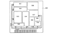
図1、図2に示す複合基板の製造装置は、貼り合わせ室101と、加熱ガス供給ユニット103を例とする熱処理手段と、第1のステージ105と、第2のステージ107と、第1のカセット室109と、第2のカセット室110と、第1の搬送手段111と、第2の搬送手段113と、第3の搬送手段115と、を有している。
The composite substrate manufacturing apparatus shown in FIGS. 1 and 2 includes a
貼り合わせ室101は、第1の基板121と第2の基板122とを貼り合わせる処理を行う場所である。
The
熱処理手段は、第2の基板122及び第2の基板122に貼り合わせられた第1の基板121を熱処理することができる。図1では貼り合わせ室101内に熱処理手段である加熱ガス供給ユニット103を設ける例を示す。このとき貼り合わせ室101は内壁を石英等で設け、加熱ガス供給ユニット103からは窒素、酸素、希ガス等のガスが所望の温度にて供給されると良い。また、加熱ガス供給ユニット103は、第2のステージ107に設けられた温度センサー125と、温度制御ユニット127とにより制御される。これらのガスにより、熱処理後の被処理基板の冷却も行うことができる。加熱ガスにて熱処理する構成とすることにより、基板面内を均一な温度にて熱処理することができる。熱処理手段による加熱は、上記高温のガスを用いて加熱を行う方式としてもよいし、ランプ光により加熱を行う方式としてもよい。ランプ光源を用いる場合、反射板を付加し、効率良く被処理基板に光が照射される構成とすることが好ましい。ランプ光源としては、例えば、棒状のハロゲンランプを用いることができる。またヒーター線を一例とする、ジュール熱にて加熱される発熱体からの輻射により加熱を行う方式としても良く、熱伝導加熱、対流加熱または輻射加熱である広い手段を用いることができる。このような熱処理手段により、貼り合わせの直後に第1の熱処理を施して、貼り合わせを強化することができる。
The heat treatment means can heat-treat the
第1のステージ105は、第1の基板121を支持するものであり、第1の基板121表面を下向きとして位置あわせをした上で固定することができる。固定方法としては、第1の基板121を真空吸着、静電吸着をすることが可能なトレイ140を設ける。図3は第2の基板122が第2のステージ107に搬送されたときの位置である。さらに、第1のステージ105は、第2の基板122一枚に対して貼り合わせる第1の基板121の枚数分のトレイ140が設けられている様子を示す。第1のステージ105の各トレイ140の位置は、第2の基板122上へ貼り合わせたときの第1の基板121の配置と一致している。また、第1のステージ105には、第1の基板121の一部に圧力を加えることができる圧力付加機構が設けられている。また第1のステージ105は、第1のステージ105を第2のステージ107に接近させたとき、第1の基板121の側面を機械的に支持する機構を有する。
The
第1のステージ105の構成の一例を図4(A)、図4(B)、図4(C)に示す。ここでは、第1の基板121表面を上向きとした状態でトレイ140に受け取り、その後第1の基板121表面を下向きにするための回転機構141が設けられる第1のステージ105の構成が示される。図4(A)のA−Bの断面図が図4(B)であり、各トレイ140には後に第1の基板121と第2の基板122とを貼り合わせるための圧力付加機構であるピン142が動作するための空間である開口部143が設けられる構造を示している。図4(B)にて圧力付加機構を動作させるとき、第1の基板121はトレイ140の吸着より解放されるが、第1のステージ105の端部が第1の基板121の端部の周りを囲うため、図4(C)のように第1の基板121の浮動を制限する。
An example of a structure of the
第2のステージ107は、第2の基板122を支持するものであり、第2の基板122表面を上向きとして位置あわせをした上で固定することができる。固定方法例としては真空吸着、静電吸着が挙げられる。又図示してはいないものの、第1のステージと第2のステージとのいずれかもしくは両方を移動させるステージ駆動部が設けられており、前記第1の基板と前記第2の基板とを近接させることができる。
The
第1のカセット室109は、第1の基板121を格納しておくものであり、第2のカセット室110は、第2の基板122を格納しておくものである。第2の基板122は第2のカセット室110に、基板表面を上向きにして格納される。
The
第1の搬送手段111は、第1の基板121を受け渡しステージ119から第1のステージ105の各トレイ140まで搬送するものである。
The
第2の搬送手段113は、第2の基板122を第2のステージ107の基板定位置まで搬送する。
The
また第3の搬送手段115は、第1の基板121を第1のカセット室109から受け渡しステージ119位置まで搬送する。
The third transfer means 115 transfers the
図1、図2のように貼り合わせ室101内に熱処理手段である加熱ガス供給ユニット103を設ける場合、貼り合わせ室101と連結して設けると良い。第1のステージ105が耐熱性の低い構造であれば、前記貼り合わせ室101内の熱処理手段を用いて基板を熱処理するとき、第1のステージ105はステージ格納室123に平行移動し格納することができる。また、図5のように、熱処理手段を内部に設けた熱処理室124を、貼り合わせ室101と連結して設けても良い。このとき第2の基板122及び第2の基板122に貼り合わせられた第1の基板121を、第2のステージ107上に載せた状態で熱処理室124に搬送し、熱処理を行う。
When the heating
図示しないが、本複合基板の製造装置には、基板洗浄手段を連結し設けていることが好ましい。洗浄手段としては、オゾン処理(例えば、オゾン水洗浄)、又は、超音波洗浄を行うことができるものが挙げられる。オゾン処理、超音波洗浄のどちらか一方でも良いし、両方を行っても良い。また、オゾン水洗浄とフッ酸による洗浄を複数回繰り返し行ってもよい。さらには洗浄機構として基板表面に純水を照射する、基板の面に平行な軸線まわりに回転して基板の面に接触するロールブラシ(PVA製)を有する洗浄装置を用いても良く、あるいは基板の面に垂直な軸線まわりに回転しつつ基板の面に接触するディスクブラシ(PVA製)を有する洗浄装置を用いても良い。また、ドライアイスを基板表面に吹き付け洗浄する方法も有効である。ドライアイスは昇華(気化)して空気中に拡散するため、表面の損傷を避けることが出来る。その他、気体を基板表面に噴射し異物を表面より飛散させることも有効である。洗浄手段は前記第1の基板表面を洗浄する機構、あるいは前記第2の基板表面を洗浄する機構、あるいは両方を備えていても良い。このような洗浄手段を設けることで、前記第1の基板と、前記第2の基板と、を貼り合せる前に両表面に付着した異物を更に効果的に除去することができる。 Although not shown, it is preferable that a substrate cleaning means is connected to the composite substrate manufacturing apparatus. Examples of the cleaning means include those capable of performing ozone treatment (for example, ozone water cleaning) or ultrasonic cleaning. Either ozone treatment or ultrasonic cleaning may be performed, or both may be performed. Further, ozone water cleaning and cleaning with hydrofluoric acid may be repeated a plurality of times. Further, as a cleaning mechanism, a cleaning device having a roll brush (made of PVA) that irradiates the substrate surface with pure water, rotates around an axis parallel to the surface of the substrate, and contacts the surface of the substrate may be used. A cleaning device having a disk brush (manufactured by PVA) that contacts the surface of the substrate while rotating around an axis perpendicular to the surface of the substrate may be used. A method of cleaning by spraying dry ice on the substrate surface is also effective. Since dry ice sublimates (vaporizes) and diffuses into the air, surface damage can be avoided. In addition, it is also effective to inject gas onto the substrate surface to scatter foreign matter from the surface. The cleaning means may include a mechanism for cleaning the surface of the first substrate, a mechanism for cleaning the surface of the second substrate, or both. By providing such a cleaning means, it is possible to more effectively remove foreign substances adhering to both surfaces before bonding the first substrate and the second substrate.
このように本実施の形態で各機能が説明される貼り合わせ室101並びに熱処理手段並びに第1のステージ105及び第2のステージ107を少なくとも有する構造であれば、本発明の装置は図1、図2の構成に限定して解釈されるものではない。例えば、第1の搬送手段111にて直接第1のカセット室109から第1のステージ105に搬送する装置構成であれば、第3の搬送手段115、及び第3の搬送手段115を備える搬送室131は設けなくても良い。
As long as the structure includes at least the
以下、図1、図2に示す装置を用い、第1の熱処理よる第1の基板121と第2の基板122とを貼り合わせる手順について説明する。尚、本実施の形態では、第1の基板121として、半導体基板の1である126mm角のシリコンウエハ、第2の基板122としてベース基板の1である600mm×720mmのガラス基板を想定して説明する。本実施の形態では第1の基板121を20枚、第2の基板122表面に貼り合わせる。すなわち第1のステージ105は、トレイ140a〜トレイ140tの計20のトレイを有し、これに対応する第1の基板121a〜第1の基板121tを処理することが出来る。尚本実施の形態では、対応しているトレイと第1の基板との機能を説明する際、トレイ140、第1の基板121と称する。こうして上記第1の搬送手段111により、第1の基板121が20枚全て第1のステージ105の各箇所に搬送される。
Hereinafter, a procedure of bonding the
まず第1の基板121を、第1のカセット室109から、第3の搬送手段115、第1の搬送手段111により、受け渡しステージ119を経由し、第1のステージ105のトレイ140の所定の位置に搬送する。ここでは第1のステージ105に搬送された第1の基板121の表面は上向きとする。その後、第1の基板121を表裏回転させ、待機させる。
First, the
第1の基板121表面を上向きにして第1の搬送手段111にて搬送する以外の方法として、第1の基板121表面を下向きとして第1の搬送手段111にて搬送し、第1のステージ105上に第1の基板121を受け渡す機構としても良い。このとき第1の基板121表面の異物の付着を低減することができる。
As a method other than the method in which the surface of the
図6(A−1)は第1の搬送手段111にて第1の基板121を支持している平面図を示している。図6(A−2)は同断面図を示している。このように、第1の搬送手段111は第1の基板121の端部を支持し第1の基板121表面を触れない状態で、第1のステージ105のトレイ140の直下に第1の基板121を搬送した後、図6(B)に示されるように第1のステージ105のトレイ140が第1の基板121の裏面を吸着し、図6(C)に示されるように第1のステージ105のトレイ140が上昇することで第1の基板121が第1のステージ105に移載される。
6A-1 is a plan view in which the
上記の一連の動作を第2の基板122に貼り合わせる第1の基板121の数だけ繰り返し、第1のステージ105の全てのトレイ140に第1の基板121を配置する。このとき第2の基板122は第2のカセット室110にあるため、上記の一連の動作に伴う発塵の影響は受けない。すなわち基板表面への異物の付着を低減することができる。
The series of operations described above is repeated as many times as the number of
この後、第1のステージ105の下方に位置される第2のステージ107上に、第2の基板122を搬送する。このとき第2のステージ107に設けられた位置調節機構により、基板の貼り合わせに係る位置(第2の基板122と第1の基板121との相対的な位置関係)が微調整される。なお、該微調整は、第2の基板122を配置した後に、第2の基板122に付したマーカー等を基準として行うようにしても良い。この場合には、例えば、マーカーの位置をアライメント用のカメラを用いて検出する方法などを用いることができる。位置調節機構として、例えば、4本の直動アクチュエータを組み合わせて用いることにより、x方向、y方向、θ方向の微調整が可能となる。
Thereafter, the
第1の基板121が配置された後には、第1のステージ105あるいは第2のステージ107、あるいはその両方を動作することにより、第2の基板122と第1の基板121とを、接触しない範囲で間隔(距離)を可能な限り小さくする。その後、前記第1の基板を、前記トレイ140から離間する。これにより前記トレイ140が前記第1の基板121を把持することにより変化していた基板の形状を、元に戻すことができる。このとき前記第1の基板121は第1のステージ105により側面を支持されており、水平方向への浮動は抑えられている。
After the
次に、第1のステージ105に供えられた圧力付加機構を用いて第1の基板121の一部に圧力を加え、圧力を加えた第1の基板121の一部から第2の基板122と第1の基板121の貼り合わせを行う。具体的には、第1の基板121の一部に対応する圧力付加機構により、第2の基板122と第1の基板121を接触させ貼り合わせを行う。前記第1の基板121の一部は、基板中央部でも角部でも良いが、本実施の形態では基板中央とする。このように、一部から貼り合わせを開始することにより、最初に貼り合わせが開始された領域から周辺に向かって貼り合わせが進行し、最終的には第1の基板121全体が第2の基板122と貼り合わせられることになる。また、図には示していないが、貼り合わせ時における第2の基板122の浮き上がりを防止する機構を設けておくことが好ましい。第2の基板122の浮き上がりを防止する機構としては、例えば、第2の基板122を第2のステージ107に押しつけておくための静電チャックなどが挙げられる。
Next, pressure is applied to a part of the
貼り合わせをより強固にするために、接触界面に掛かる圧力を徐々に大きくしても良い。例えば、エアシリンダの様な機構をトレイ140を含めた第1のステージ105に用いる構成とし、第1の基板121を第2の基板122に押圧すればよい。空気圧を用いて第1のステージ105を昇降させることにより、第2の基板122と第1の基板121との接触界面に急激な圧力が加わることを防止できるため、貼り合わせを良好に行うことができるようになる。また、第1のステージ105の第1の基板121と接触する部分を、弾性体を用いて形成する構成としても良い。この場合にも、同様に急激な圧力が加わることを防止することができる。このような圧力付加機構は、第1のステージ105に供えられることが設計上容易であるが貼り合わせ室内に設けられていれば良い。
In order to further strengthen the bonding, the pressure applied to the contact interface may be gradually increased. For example, a mechanism such as an air cylinder may be used for the
貼り合わせ室101には仕切弁129が設けられ、貼り合わせ室101を熱処理雰囲気としたときにカセット室の雰囲気を隔離することができる。貼り合わせ室101内に固定されたものは熱処理に耐えられる部材を使用する。尚排気手段(図示しない)を設け、貼り合わせの際の雰囲気を減圧雰囲気としてもよい。この場合には、雰囲気中の汚染物による影響を低減することができるため、貼り合わせに係る界面を清浄に保つことができる。また、貼り合わせの際の空気の閉じ込めを低減することができる。
A
次に、貼り合わせられた第2の基板122及び第1の基板121に対して第1の熱処理を施して、貼り合わせを強固なものとする。当該第1の熱処理は、装置内に熱処理手段が設けられている場合には該熱処理手段を用いて行う。装置内に熱処理手段が設けられていない場合であっても、できる限り第2の基板122の搬送を避け、貼り合わせ直後に行うようにする。貼り合わせ後、第1の熱処理前に第2の基板122の搬送を行う場合には、第2の基板122の撓みなどにより第1の基板121が剥離する可能性が極めて高くなるためである。本実施の形態においては装置内の熱処理手段を用いて行う場合について示すこととする。
Next, a first heat treatment is performed on the
上記第1の熱処理は、第1の基板121の上方及び第2の基板122の下方に設けられたヒーターを用いて行うことができる。貼り合わせられた基板の一方のみを加熱する場合には、第2の基板122と第1の基板121に温度差が生じ、基板に撓みが生じる可能性が高まるためである。一方で、このような撓みが問題とならない場合には、上方又は下方のいずれか一方のヒーターを用いた加熱であっても良い。加熱温度は、第2の基板122の耐熱温度以下、かつ、損傷領域の劈開が生じない温度とする必要がある。例えば、150℃以上450℃以下、好ましくは200℃以上400℃以下とすることができる。処理時間は、1分以上(好ましくは3分以上)とすれば良いが、処理速度と貼り合わせ強度との関係から最適な条件を適宜設定すればよい。本実施の形態においては、200℃、2時間の第1の熱処理を施すこととする。なお、基板の貼り合わせに係る領域にのみマイクロ波を照射することで、局所的に加熱することも可能である。なお、基板同士の貼り合わせ強度に問題がない場合には、上記第1の熱処理を省略しても良い。
The first heat treatment can be performed using a heater provided above the
その後、第1のステージ105が上昇し、第1の基板121と第1のステージ105が分離して、第2の基板122と第1の基板121との貼り合わせが終了する。
After that, the
上記方法にて、発明の複合基板の製造装置を用い第1の熱処理による貼り合わせが成されるが、続いて400℃以上750℃以下の温度範囲である第2の熱処理を行い、第1の基板121の一部、ここでは単結晶シリコン層を第2の基板122すなわちベース基板上に形成し、第1の基板121を第2の基板122より分離しても良い。このとき第2の熱処理に対し十分耐熱性を有する第1のステージ105にて第1の基板121の浮動を制限しつつ第2の熱処理を行うことで、第1の基板121が第2の基板122から分離した後に第2の基板122上を浮動し、第2の基板122表面を損傷することを避けることができる。その後各第1の基板121は、図3におけるトレイ140に吸着させ、第1の搬送手段111にて第1のカセット室109に回収することができる。
In the above method, the first substrate is bonded by the first heat treatment using the composite substrate manufacturing apparatus of the invention. Subsequently, the second heat treatment in the temperature range of 400 ° C. or higher and 750 ° C. or lower is performed. A part of the
なお、本実施の形態で示す複合基板の製造装置は、本明細書の他の実施の形態で示すSOI基板の作製方法、半導体装置の作製方法と適宜組み合わせて行うことができる。 Note that the composite substrate manufacturing apparatus described in this embodiment can be combined as appropriate with any of the methods for manufacturing an SOI substrate and semiconductor devices described in other embodiments in this specification.
(実施の形態2)
本実施の形態では、上記実施の形態1で示した複合基板の製造装置を用いたSOI基板の作製方法の一例に関して図面を参照して説明する。
(Embodiment 2)
In this embodiment, an example of a method for manufacturing an SOI substrate using the composite substrate manufacturing apparatus described in
まず、実施の形態1では第1の基板121に相当する複数の半導体基板を準備する。ここでは、半導体基板200a〜半導体基板200tの、計20枚を用いる場合について説明する。
First, in
半導体基板200a〜200tは、市販の単結晶半導体基板を用いることができ、例えば、単結晶のシリコン基板やゲルマニウム基板、ガリウムヒ素やインジウムリン等の化合物半導体基板が挙げられる。市販のシリコン基板としては、直径5インチ(125mm)、直径6インチ(150mm)、直径8インチ(200mm)、直径12インチ(300mm)サイズの円形のものが代表的である。なお、形状は円形に限られず矩形状等に加工したシリコン基板を用いることも可能である。以下の説明では、半導体基板200a〜200tとして、5インチ四方の正方形の単結晶シリコン基板を用いる場合について示す。
As the
次に、半導体基板200aの表面上に絶縁膜202aを設け、半導体基板200aの表面から所定の深さに脆化層204aを設ける(図7(A)参照)。また、半導体基板200b〜200tについても同様に、表面上に絶縁膜202b〜202tをそれぞれ設け、表面から所定の深さに脆化層204b〜200tをそれぞれ設ける。
Next, the insulating
絶縁膜202a〜202tは、例えば、酸化シリコン膜、酸化窒化シリコン膜、窒化シリコン膜、窒化酸化シリコン膜等の単層、又はこれらを積層させた膜を用いることができる。これらの膜は、熱酸化法、CVD法又はスパッタリング法等を用いて形成することができる。また、CVD法を用いて絶縁膜202a〜202tを形成する場合には、テトラエトキシシラン(略称;TEOS:化学式Si(OC2H5)4)等の有機シランを用いて作製される酸化シリコン膜を絶縁膜202a〜202tに用いることができる。
As the insulating
例えば、半導体基板200a〜200t上に酸化窒化シリコン膜と窒化酸化シリコン膜を順に積層させて形成した後、半導体基板200a〜200tの表面から所定の深さの領域にイオンを導入し、その後、CVD法によりテトラエトキシシランを用いて作製される酸化シリコン膜を窒化酸化シリコン膜上に形成してもよい。
For example, after a silicon oxynitride film and a silicon nitride oxide film are sequentially stacked over the
なお、酸化窒化シリコン膜とは、その組成として、窒素よりも酸素の含有量が多いものであって、ラザフォード後方散乱法(RBS:Rutherford Backscattering Spectrometry)、及び水素前方散乱法(HFS:Hydrogen Foward Scattering)を用いて測定した場合に、濃度範囲として酸素が50〜70原子%、窒素が0.5〜15原子%、Siが25〜35原子%、水素が0.1〜10原子%の範囲で含まれるものをいう。また、窒化酸化シリコン膜とは、その組成として、酸素よりも窒素の含有量が多いものであって、RBS及びHFSを用いて測定した場合に、濃度範囲として酸素が5〜30原子%、窒素が20〜50原子%、Siが25〜35原子%、水素が15〜25原子%の範囲で含まれるものをいう。但し、酸化窒化シリコンまたは窒化酸化シリコンを構成する原子の合計を100原子%としたとき、窒素、酸素、Si及び水素の含有比率が上記の範囲内に含まれるものとする。 Note that the silicon oxynitride film has a composition that contains more oxygen than nitrogen, and includes Rutherford Backscattering (RBS) and Hydrogen Forward Scattering (HFS). ) In the range of 50 to 70 atomic% oxygen, 0.5 to 15 atomic% nitrogen, 25 to 35 atomic% Si, and 0.1 to 10 atomic% hydrogen. It means what is included. In addition, the silicon nitride oxide film has a composition containing more nitrogen than oxygen. When measured using RBS and HFS, the concentration range of oxygen is 5 to 30 atomic%, nitrogen. Is contained in the range of 20-50 atomic%, Si is 25-35 atomic%, and hydrogen is 15-25 atomic%. However, when the total number of atoms constituting silicon oxynitride or silicon nitride oxide is 100 atomic%, the content ratio of nitrogen, oxygen, Si, and hydrogen is included in the above range.
次いで表面から電界で加速されたイオンを所定の深さに水素をイオンドープ法またはイオン注入法で照射する事によって脆化層204a〜204tを形成する。ここで意味するイオン注入はイオンの質量分離を行うことを意味し、イオンドープはイオンの質量分離を行わないことを意味する。イオンドープまたはイオン注入はベース基板に転置するSOI層の厚さを考慮して行われる。当該SOI層の厚さは5nm乃至500nm、好ましくは10nm乃至200nm、更に好ましくは10nm乃至100nm、更に好ましくは10nm乃至50nmの厚さとする。イオンをイオンドープまたはイオン注入する際の加速電圧はこのような厚さを考慮して、半導体基板200a〜200tにイオンドープまたはイオン注入されるようにする。なお、剥離後にSOI層の表面をCMP(ケミカルメカニカルポリッシング)等の研磨工程によって研磨または溶融して平坦化するため、剥離直後のSOI層の厚さは50nm乃至500nmとしておくことが好ましい。
Next, the embrittled
上記脆化層204a〜204tの形成にあたり、イオンドープ法において、H+イオンでも良いが、H3 +イオン若しくはH2 +イオンの何れかを主イオンとしてもよい。また、イオン注入法において、H+イオンでも良いが、水素のクラスターイオンであるH3 +やH2 +をイオン注入してもよい。脆化層204a〜204tは、水素イオンのみでなく希ガスイオンを用いてもよく、或いは両者を混合させて用いてもよい。また、脆化層204a〜204tを形成する前に、半導体基板表面に、自然酸化膜、ケミカルオキサイド、又は酸素を含む雰囲気でUV光を照射することにより形成された酸化膜を形成しておくことが好ましい。ここで、ケミカルオキサイドは、オゾン水、過酸化酸素水、硫酸等の酸化剤でボンドウエハ表面を処理することにより形成することができる。また、熱酸化膜、シラン系のガスを用いてCVD法で成膜した酸化珪素膜、酸化窒化珪素膜、窒化酸化珪素膜などを脆化層204a〜204tを形成する前に形成してもよい。半導体基板表面に酸化膜を形成しておくことで、脆化層204a〜204tを形成する際の半導体基板表面のエッチングによる表面荒れを防ぐことができる。
In forming the
次に、実施の形態1では第2の基板122に相当するベース基板220を準備する(図7(B)参照)。ここではベース基板220の形状は、600×720mmの長方形を例に説明する。
Next, in
ベース基板220は、絶縁体でなる基板を用いる。具体的には、ベース基板220として、アルミノシリケートガラス、アルミノホウケイ酸ガラス、バリウムホウケイ酸ガラスのような電子工業用に使われるガラス基板を用いる。ベース基板220として大面積化が可能で安価なガラス基板を用いることにより、シリコンウエハを用いる場合と比較して低コスト化を図ることができる。
As the
ベース基板220の表面には、絶縁膜を設けても良い。該絶縁膜が設けられていることにより、ベース基板からアルカリ金属などの不純物が拡散して半導体膜が汚染することを防ぐことができる。絶縁膜の材料としては、十分な平坦性が得られるのであれば、PECVD法またはスパッタ法により得られる酸化珪素膜、酸化窒化珪素膜、窒化酸化珪素膜、窒化珪素膜、窒化ゲルマニウム膜、酸化窒化ゲルマニウム膜、窒化酸化ゲルマニウム膜などのシリコンまたはゲルマニウムを組成に含む絶縁膜を用いることができる。また、酸化アルミニウム、酸化タンタル、酸化ハフニウムなどの金属の酸化物でなる絶縁膜、窒化アルミニウムなどの金属の窒化物でなる絶縁膜、酸化窒化アルミニウム膜などの金属の酸化窒化物でなる絶縁膜、窒化酸化アルミニウム膜などの金属の窒化酸化物でなる絶縁膜を用いることもできる。勿論、ベース基板220の表面に何も形成しなくても良い。本実施の形態では何も形成しない構造を例とする。
An insulating film may be provided on the surface of the
次に、複数の半導体基板200a〜200tの表面とベース基板220の表面とを対向させ、絶縁膜202a〜202tとベース基板220とをそれぞれ貼り合わせる(図7(C)参照)。この貼り合わせ処理は、上記実施の形態1で示した複合基板の製造装置を用いて行う。第1のステージ205内の各トレイに接着された半導体基板200a〜200tの、それぞれ形成された絶縁膜202a〜202tと、第2のステージ206に接着されたベース基板220の表面とを近接し、実施の形態1のように貼り合せることにより接合が形成される。この接合は、ファンデルワールス力が作用しており、半導体基板200a〜200tとベース基板220を圧接することにより、Si−OH等を結合種として、水素結合による接合を形成することが可能となる。
Next, the surfaces of the plurality of
なお、半導体基板200a〜200tをベース基板220に貼り合わせる前に、半導体基板200a〜200t上に形成された絶縁膜202a〜202tと、ベース基板220の表面処理を行うことが好ましい。表面処理としては、オゾン処理(例えば、オゾン水洗浄)、又は、超音波洗浄を行うことができる。オゾン処理、超音波洗浄のどちらか一方でも良いし、両方を行っても良い。また、オゾン水洗浄とフッ酸による洗浄を複数回繰り返し行ってもよい。このような表面処理を行うことにより、絶縁膜202a〜202t、ベース基板220表面の有機物等のゴミを除去し、表面を親水化することができる。
Note that before the
他にも、表面処理としてプラズマ処理による表面処理を行ってもよい。例えば、真空状態のチャンバーに不活性ガス(例えば、Arガス)及び/又は反応性ガス(例えば、O2ガス、N2ガス)を導入し、被処理面(ここでは、ベース基板220又は絶縁膜202a〜202t)にバイアス電圧を印加してプラズマ状態として行う。プラズマ中には電子とArの陽イオンが存在し、陰極方向(被処理面側)にArの陽イオンが加速される。加速されたArの陽イオンが被処理面に衝突することによって、被処理面をスパッタエッチングすることができる。このとき、被処理面の凸部から優先的にスパッタエッチングされ、当該被処理面の平坦性を向上することができる。このような処理室を本発明の複合基板の製造装置に連結してもよい。また、このような表面処理を行っても、絶縁膜202a〜202t、ベース基板220表面を親水化することができる。さらに上記プラズマ処理を、上記オゾン処理等の洗浄と組み合わせても良い。
In addition, surface treatment by plasma treatment may be performed as the surface treatment. For example, an inert gas (for example, Ar gas) and / or a reactive gas (for example, O 2 gas or N 2 gas) is introduced into a vacuum chamber, and a surface to be processed (here, the
次に、熱処理を行い脆化層204a〜204cにて分離(劈開)することにより、ベース基板220上に、絶縁膜202a〜202cを介して単結晶半導体膜224a〜224cを設ける(図7(D)参照)。ここでは、400℃以上750℃以下の第2の熱処理を行うことにより、半導体基板の脆化層に含まれる微小な空洞の体積変化が起こり、当該脆化層に沿って分離することが可能となる。熱処理装置として、被処理基板であるベース基板220及び半導体基板の急速加熱を行うことができる構成とすることにより、熱処理時間の短縮化を図ることができる。また、ベース基板220の歪点より高い温度が利用できる。第2の熱処理は、高温のガスを用いて加熱を行う方式(Gas Rapid Thermal Anneal)としてもよいし、ランプ光により加熱を行う方式(Lamp Rapid Thermal Anneal)としてもよい。
Next, heat treatment is performed to separate (cleave) the embrittled
前記第2の熱処理も、実施の形態1に示される本発明の複合基板の製造装置にて処理することができる。このとき第1のステージ105を半導体基板に接触させつつ第2の熱処理を行うことで、半導体基板がベース基板から分離した後にベース基板上を浮動し、ベース基板表面を損傷することを避けることができる。その後各半導体基板は、図1における第1のステージ105に吸着させ、第1の搬送手段111にて第1のカセット室109に回収することができる。
The second heat treatment can also be processed by the composite substrate manufacturing apparatus of the present invention shown in the first embodiment. At this time, by performing the second heat treatment while the
以上の工程により、ベース基板220上に、それぞれ絶縁膜202a〜絶縁膜202cを介して単結晶半導体膜224a〜224cが設けられたSOI基板を作製することができる。
Through the above steps, an SOI substrate in which the single
なお、上記工程において、得られたSOI基板の表面に平坦化処理を行ってもよい。平坦化処理を行うことにより、剥離後にベース基板220上に設けられた単結晶半導体膜224a〜224cの表面に凹凸が生じた場合でもSOI基板の表面を平坦化することができる。
Note that in the above steps, planarization treatment may be performed on the surface of the obtained SOI substrate. By performing the planarization treatment, the surface of the SOI substrate can be planarized even when unevenness is generated on the surfaces of the single
平坦化処理としては、CMP(Chemical Mechanical Polishing)、エッチング処理、レーザー光の照射等により行うことができる。ここでは、ドライエッチングまたはウエットエッチングの一方、または双方を組み合わせたエッチング処理(エッチバック処理)を行った後にレーザー光を照射することによって、単結晶半導体膜224a〜224cの再結晶化と表面の平坦化を行う。
The planarization treatment can be performed by CMP (Chemical Mechanical Polishing), etching treatment, laser light irradiation, or the like. Here, the single
レーザー光を単結晶半導体膜の上面側から照射することで、単結晶半導体膜の上面を溶融させることができる。溶融した後、単結晶半導体膜が冷却、固化することで、その上面の平坦性が向上した単結晶半導体膜が得られる。レーザー光を用いることにより、ベース基板220が直接加熱されないため、当該ベース基板220の温度上昇を抑えることができる。このため、ガラス基板のような耐熱性の低い基板をベース基板220に用いることが可能である。
By irradiating laser light from the upper surface side of the single crystal semiconductor film, the upper surface of the single crystal semiconductor film can be melted. After melting, the single crystal semiconductor film is cooled and solidified, whereby a single crystal semiconductor film with improved flatness on the upper surface is obtained. By using laser light, the
なお、レーザー光の照射による単結晶半導体膜の溶融は、部分溶融とすることが好ましい。完全溶融させた場合には、液相となった後の無秩序な核発生により微結晶化し、結晶性が低下する可能性が高いためである。一方で、部分溶融させることにより、溶融されていない固相部分から結晶成長が進行する。これにより、半導体膜中の欠陥を減少させることができる。ここで、完全溶融とは、単結晶半導体膜が下部界面付近まで溶融されて、液体状態になることをいう。他方、部分溶融とは、この場合、単結晶半導体膜の上部は溶融して液相となるが、下部は溶融せずに固相のままであることをいう。 Note that melting of the single crystal semiconductor film by laser light irradiation is preferably partial melting. This is because, when completely melted, there is a high possibility that the crystallinity is lowered due to disordered nucleation after the liquid phase is formed and the crystallinity is lowered. On the other hand, by partial melting, crystal growth proceeds from a solid phase portion that is not melted. Thereby, defects in the semiconductor film can be reduced. Here, complete melting means that the single crystal semiconductor film is melted to the vicinity of the lower interface to be in a liquid state. On the other hand, partial melting means that in this case, the upper part of the single crystal semiconductor film is melted into a liquid phase, but the lower part is not melted and remains in a solid phase.
上記レーザー光の照射には、パルス発振レーザーを用いることが好ましい。これは、瞬間的に高エネルギーのパルスレーザー光を発振することができ、溶融状態を作り出すことが容易となるためである。発振周波数は、1Hz以上10MHz以下程度とすることが好ましい。 A pulsed laser is preferably used for the laser light irradiation. This is because high-energy pulsed laser light can be instantaneously oscillated, and it becomes easy to create a molten state. The oscillation frequency is preferably about 1 Hz to 10 MHz.
上述のようにレーザー光を照射した後には、単結晶半導体膜の膜厚を小さくする薄膜化工程を行っても良い。単結晶半導体膜の薄膜化には、ドライエッチングまたはウエットエッチングの一方、または双方を組み合わせたエッチング処理(エッチバック処理)を適用すればよい。例えば、単結晶半導体膜がシリコン材料からなる層である場合、ドライエッチングとしてSF6と02をプロセスガスに用いて、単結晶半導体膜を薄くすることができる。 After the laser light irradiation as described above, a thinning process for reducing the thickness of the single crystal semiconductor film may be performed. In order to reduce the thickness of the single crystal semiconductor film, an etching process (etchback process) in which one of dry etching or wet etching or a combination of both is applied may be applied. For example, when the single crystal semiconductor film is a layer made of a silicon material, the single crystal semiconductor film can be thinned by using SF6 and 02 as a process gas as dry etching.
なお、平坦化処理はSOI基板に限らず分離後の半導体基板200a〜200tに対して行ってもよい。分離後の半導体基板200a〜200tの表面を平坦にすることによって、当該半導体基板200a〜200tをSOI基板の作製工程において再利用することが可能となる。
Note that the planarization process is not limited to the SOI substrate, and may be performed on the separated
なお、本実施の形態で示したSOI基板の作製方法は、本明細書の他の実施の形態で示す作製方法と適宜組み合わせて行うことができる。 Note that the method for manufacturing an SOI substrate described in this embodiment can be combined with manufacturing methods described in other embodiments in this specification as appropriate.
(実施の形態3)
本実施の形態では、上記実施の形態2で作製したSOI基板を用いて、薄膜トランジスタ(TFT)を作製する方法を説明する。
(Embodiment 3)
In this embodiment, a method for manufacturing a thin film transistor (TFT) using the SOI substrate manufactured in
まず、図12および図13を参照して、nチャネル型薄膜トランジスタ、およびpチャネル型薄膜トランジスタを作製する方法を説明する。複数の薄膜トランジスタ(TFT)を組み合わせることで、各種の半導体装置を形成することができる。 First, a method for manufacturing an n-channel thin film transistor and a p-channel thin film transistor is described with reference to FIGS. Various semiconductor devices can be formed by combining a plurality of thin film transistors (TFTs).
SOI基板として、上記実施の形態2の方法で作製したSOI基板を用いる場合について説明する。
A case where an SOI substrate manufactured by the method of
図12(A)は、図3を用いて説明した方法で作製されたSOI基板の断面図である。 FIG. 12A is a cross-sectional view of an SOI substrate manufactured by the method described with reference to FIGS.
エッチングにより、単結晶半導体膜224aをパターニングして、図12(B)に示すように半導体膜251、252を形成する。半導体膜251はnチャネル型のTFTを構成し、半導体膜252はpチャネル型のTFTを構成する。
The single
図12(C)に示すように、半導体膜251、252上に絶縁膜254を形成する。次に、絶縁膜254を介して半導体膜251上にゲート電極255を形成し、半導体膜252上にゲート電極256を形成する。
As shown in FIG. 12C, an insulating
なお、単結晶半導体膜224aのエッチングを行う前に、TFTのしきい値電圧を制御するために、ホウ素、アルミニウム、ガリウムなどのp型を付与する不純物元素、またはリン、ヒ素などのn型を付与する不純物元素を単結晶半導体膜224aに添加することが好ましい。例えば、nチャネル型TFTが形成される領域にp型を付与する不純物元素を添加し、pチャネル型TFTが形成される領域にn型を付与する不純物元素を添加する。
Note that an impurity element imparting a p-type such as boron, aluminum, or gallium, or an n-type such as phosphorus or arsenic is used to control the threshold voltage of the TFT before etching the single
次に、図12(D)に示すように半導体膜251にn型の低濃度不純物領域257を形成し、半導体膜252にp型の高濃度不純物領域259を形成する。具体的には、まず、半導体膜251にn型の低濃度不純物領域257を形成する。このため、pチャネル型TFTとなる半導体膜252をレジストでマスクし、不純物元素を半導体膜251に添加する。不純物元素としてリンまたはヒ素を添加すればよい。イオンドーピング法またはイオン注入法により不純物元素を添加することにより、ゲート電極255がマスクとなり、半導体膜251に自己整合的にn型の低濃度不純物領域257が形成される。半導体膜251のゲート電極255と重なる領域はチャネル形成領域258となる。
Next, as illustrated in FIG. 12D, an n-type low
次に、半導体膜252を覆うマスクを除去した後、nチャネル型TFTとなる半導体膜251をレジストマスクで覆う。次に、イオンドーピング法またはイオン注入法により不純物元素を半導体膜252に添加する。不純物元素として、ボロンを添加することができる。不純物元素の添加工程では、ゲート電極256がマスクとして機能して、半導体膜252にp型の高濃度不純物領域259が自己整合的に形成される。p型の高濃度不純物領域259はソース領域またはドレイン領域として機能する。半導体膜252のゲート電極256と重なる領域はチャネル形成領域260となる。ここでは、n型の低濃度不純物領域257を形成した後、p型の高濃度不純物領域259を形成する方法を説明したが、先にp型の高濃度不純物領域259を形成することもできる。
Next, after removing the mask covering the
次に、半導体膜251を覆うレジストを除去した後、プラズマCVD法等によって窒化シリコン等の窒素化合物や酸化シリコン等の酸化物からなる単層構造または積層構造の絶縁膜を形成する。この絶縁膜を垂直方向の異方性エッチングすることで、図13(A)に示すように、ゲート電極255、256の側面に接するサイドウォール絶縁膜261、262を形成する。この異方性エッチングにより、絶縁膜254もエッチングされる。
Next, after removing the resist covering the
次に、図13(B)に示すように、半導体膜252をレジスト265で覆う。半導体膜251にソース領域またはドレイン領域として機能する高濃度不純物領域を形成するため、イオン注入法またはイオンドーピング法により、半導体膜251に高ドーズ量で不純物元素を添加する。ゲート電極255およびサイドウォール絶縁膜261がマスクとなり、n型の高濃度不純物領域267が形成される。次に、不純物元素の活性化のための熱処理を行う。
Next, as illustrated in FIG. 13B, the
活性化の熱処理の後、図13(C)に示すように、水素を含んだ絶縁膜268を形成する。絶縁膜268を形成後、350℃以上450℃以下の温度による熱処理を行い、絶縁膜268中に含まれる水素を半導体膜251、252中に拡散させる。絶縁膜268は、プロセス温度が350℃以下のプラズマCVD法により窒化シリコンまたは窒化酸化シリコンを堆積することで形成できる。半導体膜251、252に水素を供給することで、半導体膜251、252中および絶縁膜254との界面での捕獲中心となるような欠陥を効果的に補償することができる。
After the heat treatment for activation, an insulating
その後、層間絶縁膜269を形成する。層間絶縁膜269は、酸化シリコン膜、BPSG(Boron Phosphorus Silicon Glass)膜などの無機材料でなる絶縁膜、または、ポリイミド、アクリルなどの有機樹脂膜から選ばれた単層構造の膜、積層構造の膜で形成することができる。層間絶縁膜269にコンタクトホールを形成した後、図13(C)に示すように配線270を形成する。配線270の形成には、例えば、アルミニウム膜またはアルミニウム合金膜などの低抵抗金属膜をバリアメタル膜で挟んだ3層構造の導電膜で形成することができる。バリアメタル膜は、モリブデン、クロム、チタンなどの金属膜で形成することができる。
Thereafter, an
以上の工程により、nチャネル型TFTとpチャネル型TFTを有する半導体装置を作製することができる。SOI基板の作製過程で、チャネル形成領域を構成する半導体膜の金属元素の濃度を低減させているので、オフ電流が小さく、しきい値電圧の変動が抑制されたTFTを作製することができる。 Through the above steps, a semiconductor device having an n-channel TFT and a p-channel TFT can be manufactured. In the process of manufacturing the SOI substrate, the concentration of the metal element in the semiconductor film forming the channel formation region is reduced, so that a TFT with a small off-state current and a suppressed threshold voltage can be manufactured.
(実施の形態4)
本実施の形態では、上記実施の形態と異なる薄膜トランジスタの作製方法に関して図面を参照して説明する。本実施の形態に示す薄膜トランジスタの製造方法では、半導体膜と配線との接続に係る開口が自己整合的に形成されることを特徴としている。
(Embodiment 4)
In this embodiment, a method for manufacturing a thin film transistor, which is different from that in the above embodiment, will be described with reference to drawings. The manufacturing method of the thin film transistor described in this embodiment is characterized in that an opening related to the connection between the semiconductor film and the wiring is formed in a self-aligning manner.
はじめに、上記実施の形態2で示した方法を用いて作製したSOI基板を用意する。そして、該SOI基板における半導体膜を島状にパターニングして島状半導体膜906を形成した後、ゲート絶縁膜として機能する絶縁膜908、及びゲート電極(又は配線)として機能する導電膜を順に形成する。本実施の形態では、ゲート電極として機能する導電膜を二層構造で形成するが、本発明はこれに限定されるものではない。ここで、絶縁膜908は、酸化珪素、酸化窒化珪素、窒化酸化珪素、窒化珪素などの材料を用いて、CVD法やスパッタリング法などにより形成することができる。絶縁膜908の厚さは5nm以上100nm以下程度とすれば良い。また、導電膜は、タンタル(Ta)、タングステン(W)、チタン(Ti)、モリブデン(Mo)、アルミニウム(Al)、銅(Cu)、クロム(Cr)、ニオブ(Nb)等の材料を用いて、CVD法やスパッタリング法などにより形成することができる。導電膜の厚さは、二層の合計が100nm以上500nm以下程度となるようにすれば良い。なお、本実施の形態では、絶縁膜908を酸化珪素(厚さ20nm)にて形成し、導電膜(下層)を窒化タンタル(厚さ50nm)にて形成し、導電膜(上層)をタングステン(厚さ200nm)にて形成する場合について説明する。
First, an SOI substrate manufactured using the method described in
なお、上記の半導体膜には、薄膜トランジスタの閾値電圧を制御するために、硼素、アルミニウム、ガリウムなどのp型を付与する不純物や、リン、砒素などのn型を付与する不純物を添加しても良い。例えば、p型を付与する不純物として硼素を添加する場合、5×1016cm−3以上1×1017cm−3以下の濃度で添加すれば良い。また、半導体膜に対して水素化処理を行っても良い。水素化処理は、例えば、水素雰囲気中において350℃、2時間程度行う。
Note that an impurity imparting a p-type such as boron, aluminum, or gallium or an impurity imparting an n-type such as phosphorus or arsenic may be added to the semiconductor film in order to control the threshold voltage of the thin film transistor. good. For example, when boron is added as an impurity imparting p-type conductivity, it may be added at a concentration of 5 × 10 16
次に、上記のゲート電極として機能する導電膜をパターニングする。なお、本実施の形態における薄膜トランジスタの製造方法では、上記の導電膜に対して少なくとも二度のパターニングを行うが、ここでは、そのうちの一度目のパターニングを行う。これにより、最終的に形成されるゲート電極より一回り大きい導電膜910、及び導電膜912が形成される。ここで、「一回り大きい」とは、二度目のパターニング工程において用いられるゲート電極形成用のレジストマスクを、導電膜910、及び導電膜912の位置に合わせて形成できる程度の大きさをいうものとする。なお、上記二度のパターニングは、導電膜の島状半導体膜906と重なる領域に対して行えば良いものであり、導電膜全面に対して二度のパターニングを行う必要はない。
Next, the conductive film functioning as the gate electrode is patterned. Note that in the method for manufacturing a thin film transistor in this embodiment, the conductive film is patterned at least twice, but here, the first patterning is performed. Thus, a
その後、上記の絶縁膜908、導電膜910、及び導電膜912を覆うように、絶縁膜914を形成する(図15(A)、図17(A)参照)。ここで、絶縁膜914は、酸化珪素、酸化窒化珪素、窒化酸化珪素、窒化珪素、酸化ハフニウム、酸化アルミニウムなどの材料を用いて、CVD法やスパッタリング法などにより形成することができる。絶縁膜914の厚さは0.5μm以上2μm以下程度とすることが好ましい。本実施の形態では、一例として、絶縁膜914を酸化珪素(厚さ1μm)にて形成する場合について説明する。なお、本実施の形態においては、ベース基板900上に、絶縁膜904、及び半導体膜が順に設けられた構造のSOI基板を用いて説明しているが、本発明はこれに限定して解釈されるものではない。
After that, an insulating
なお、図15(A)は、平面図である図17(A)のP−Qにおける断面に対応する図である。同様に、図15(B)と図17(B)が対応し、図15(D)と図17(C)が対応し、図16(C)と図17(D)が対応する。図17に示す平面図では、簡単のため、対応する断面図における一部の構成要素を省略している。 Note that FIG. 15A is a diagram corresponding to a cross section taken along a line PQ in FIG. 17A which is a plan view. Similarly, FIG. 15B corresponds to FIG. 17B, FIG. 15D corresponds to FIG. 17C, and FIG. 16C corresponds to FIG. 17D. In the plan view shown in FIG. 17, some components in the corresponding cross-sectional views are omitted for simplicity.
次に、上記の絶縁膜914上に、パターニング工程において用いるゲート電極形成用のレジストマスク916を形成する。該パターニング工程は、上記導電膜に対する二度のパターニングのうち、二度目のパターニング工程に当たるものである。レジストマスク916は、感光性物質であるレジスト材料を塗布した後、パターンを露光することで形成できる。レジストマスク916の形成後には、該レジストマスク916を用いて、導電膜910、導電膜912、及び絶縁膜914をパターニングする。具体的には絶縁膜914を選択的にエッチングして絶縁膜922を形成した後、導電膜910、及び導電膜912を選択的にエッチングしてゲート電極として機能する導電膜918、導電膜920を形成する(図15(B)、図17(B)参照)。ここで、絶縁膜914を選択的にエッチングする際には、ゲート絶縁膜として機能する絶縁膜908の一部も図15(B)のように、同時にエッチングされる。
Next, a resist
次に、レジストマスク916を除去した後、島状半導体膜906、絶縁膜908、導電膜918、導電膜920、絶縁膜922などを覆うように、絶縁膜924を形成する。絶縁膜924は後のサイドウォール形成時のバリア層として機能する。絶縁膜924は、酸化珪素、酸化窒化珪素、窒化酸化珪素、窒化珪素、酸化ハフニウム、酸化アルミニウム、酸化タンタルなどの材料を用いて形成することができるが、バリア層として機能させるためには、後のサイドウォールに用いられる材料とエッチング時の選択比が取れる材料を用いて形成することが好ましいと言える。絶縁膜924の厚さは10nm以上200nm以下程度とすれば良い。本実施の形態では、絶縁膜924を、窒化珪素(厚さ50nm)を用いて形成することとする。
Next, after the resist
絶縁膜924の形成後には、導電膜918、導電膜920、絶縁膜922等をマスクとして、一導電型を付与する不純物元素を島状半導体膜906に添加する。本実施の形態では、島状半導体膜906にn型を付与する不純物元素(例えばリンや砒素)を添加する。該不純物の添加により、島状半導体膜906に不純物領域926が形成される(図15(C)参照)。なお、本実施の形態においては、絶縁膜924を形成した後に、n型を付与する不純物元素を添加する構成としたが、本発明はこれに限られない。例えば、レジストマスクを除去した後、又は除去する前に上記の不純物元素を添加し、その後、絶縁膜924を形成する構成としてもよい。また、添加する不純物元素を、p型を付与する不純物元素とすることもできる。
After the insulating
次に、サイドウォール928を形成する(図15(D)、図17(C)参照)。サイドウォール928は、絶縁膜924を覆うように絶縁膜を形成し、該絶縁膜に対して垂直方向を主体とした異方性エッチングを適用することで形成することができる。上記異方性エッチングにより、絶縁膜が選択的にエッチングされることになるためである。絶縁膜は、酸化珪素、酸化窒化珪素、窒化酸化珪素、窒化珪素、酸化ハフニウム、酸化アルミニウム、酸化タンタルなどの材料を用いて、CVD法やスパッタリング法などにより形成することができる。また、有機材料を含む膜を、スピンコートなどにより形成しても良い。本実施の形態においては、絶縁膜の材料として酸化珪素を用いることとする。すなわち、サイドウォール928は酸化珪素により形成される。また、上記エッチングガスとしては、例えば、CHF3とヘリウムの混合ガスを用いることができる。なお、サイドウォール928を形成する工程はこれらに限定されない。
Next, a
次に、絶縁膜922、サイドウォール928などをマスクとして、島状半導体膜906に一導電型を付与する不純物元素を添加する。なお、島状半導体膜906には、先の工程で添加した不純物元素と同じ導電型の不純物元素をより高い濃度で添加する。つまり、本実施の形態においては、n型を付与する不純物元素を添加することになる。
Next, an impurity element imparting one conductivity type is added to the island-shaped
上記不純物元素の添加により、島状半導体膜906に、チャネル形成領域930と、低濃度不純物領域932と、高濃度不純物領域934が形成される。低濃度不純物領域932はLDD(Lightly Doped Drain)領域として機能し、高濃度不純物領域934はソース又はドレインとして機能する。
By the addition of the impurity element, a
次に、絶縁膜924をエッチングして、高濃度不純物領域に達する開口(コンタクトホール)を形成する(図16(A)参照)。本実施の形態においては、酸化珪素を用いて絶縁膜922、及びサイドウォール928を形成し、窒化珪素を用いて絶縁膜924を形成しているため、絶縁膜924を選択的にエッチングして開口を形成することができる。
Next, the insulating
上記高濃度不純物領域に達する開口を形成した後、絶縁膜914を選択的にエッチングすることにより、開口936を形成する(図16(B)参照)。開口936は、高濃度不純物領域に達する開口と比較して大きく形成されることになる。これは、開口936は、プロセスルールやデザインルールに従ってその最小線幅が決まるのに対して、高濃度不純物領域に達する開口は、自己整合的に形成されることでより微細化されるためである。
After the opening reaching the high-concentration impurity region is formed, the insulating
その後、上記高濃度不純物領域に達する開口及び開口936を介して、島状半導体膜906の高濃度不純物領域934及び導電膜920に接する導電膜を形成する。該導電膜は、CVD法やスパッタリング法等により形成することができる。材料としては、アルミニウム(Al)、タングステン(W)、チタン(Ti)、タンタル(Ta)、モリブデン(Mo)、ニッケル(Ni)、白金(Pt)、銅(Cu)、金(Au)、銀(Ag)、マンガン(Mn)、ネオジム(Nd)、炭素(C)、珪素(Si)等を用いることができる。また、上記金属を主成分とする合金を用いても良いし、上記金属を含む化合物を用いても良い。また、上記導電膜は、単層構造としても良いし、積層構造としても良い。本実施の形態においては、チタンとアルミニウムとチタンとの三層構造とする場合を示す。
After that, a conductive film in contact with the high
上記導電膜を選択的にエッチングすることにより、ソース電極又はドレイン電極(ソース配線又はドレイン配線)として機能する導電膜938、導電膜940及び導電膜942、導電膜920と接続されて配線として機能する導電膜944、導電膜946及び導電膜948を形成する(図16(C)、図17(D)参照)。以上の工程により、島状半導体膜906と、ソース電極又はドレイン電極として機能する導電膜との接続を自己整合的に形成した薄膜トランジスタが完成する。
By selectively etching the conductive film, the
本実施の形態において示した方法により、ソース電極又はドレイン電極の接続関係を自己整合的に形成することができるため、トランジスタの構造を微細化することができる。つまり、半導体素子の集積度を向上することができるようになる。また、チャネル長や低濃度不純物領域の長さを自己整合的に規定することができるため、微細化において問題となるチャネル抵抗のばらつきを抑制することができる。すなわち、特性の優れたトランジスタを提供することができる。 With the method described in this embodiment, the connection relation between the source electrode and the drain electrode can be formed in a self-aligned manner, so that the structure of the transistor can be miniaturized. That is, the degree of integration of the semiconductor elements can be improved. In addition, since the channel length and the length of the low-concentration impurity region can be defined in a self-aligned manner, variation in channel resistance, which is a problem in miniaturization, can be suppressed. That is, a transistor with excellent characteristics can be provided.
(実施の形態5)
本実施の形態では、上記実施の形態で示した薄膜トランジスタを適用した半導体装置の具体的な態様について図面を参照して説明する。
(Embodiment 5)
In this embodiment, specific modes of a semiconductor device to which the thin film transistor described in any of the above embodiments is applied will be described with reference to drawings.
まず、半導体装置の一例として、マイクロプロセッサについて説明する。図8はマイクロプロセッサ500の構成例を示すブロック図である。
First, a microprocessor will be described as an example of a semiconductor device. FIG. 8 is a block diagram illustrating a configuration example of the
マイクロプロセッサ500は、演算回路501(Arithmetic logic unit。ALUともいう。)、演算回路制御部502(ALU Controller)、命令解析部503(Instruction Decoder)、割り込み制御部504(Interrupt Controller)、タイミング制御部505(Timing Controller)、レジスタ506(Register)、レジスタ制御部507(Register Controller)、バスインターフェース508(Bus I/F)、読み出し専用メモリ509、およびメモリインターフェース510を有している。
The
バスインターフェース508を介してマイクロプロセッサ500に入力された命令は、命令解析部503に入力され、デコードされた後、演算回路制御部502、割り込み制御部504、レジスタ制御部507、タイミング制御部505に入力される。演算回路制御部502、割り込み制御部504、レジスタ制御部507、タイミング制御部505は、デコードされた命令に基づき様々な制御を行う。
An instruction input to the
演算回路制御部502は、演算回路501の動作を制御するための信号を生成する。また、割り込み制御部504は、マイクロプロセッサ500のプログラム実行中に、外部の入出力装置や周辺回路からの割り込み要求を処理する回路であり、割り込み制御部504は、割り込み要求の優先度やマスク状態を判断して、割り込み要求を処理する。レジスタ制御部507は、レジスタ506のアドレスを生成し、マイクロプロセッサ500の状態に応じてレジスタ506の読み出しや書き込みを行う。タイミング制御部505は、演算回路501、演算回路制御部502、命令解析部503、割り込み制御部504、およびレジスタ制御部507の動作のタイミングを制御する信号を生成する。例えば、タイミング制御部505は、基準クロック信号CLK1を元に、内部クロック信号CLK2を生成する内部クロック生成部を備えている。図8に示すように、内部クロック信号CLK2は他の回路に入力される。
The arithmetic
次に、非接触でデータの送受信を行う機能、および演算機能を備えた半導体装置の一例を説明する。図9は、このような半導体装置の構成例を示すブロック図である。図9に示す半導体装置は、無線通信により外部装置と信号の送受信を行って動作するコンピュータ(以下、「RFCPU」という)と呼ぶことができる。 Next, an example of a semiconductor device having a function of performing transmission / reception of data without contact and an arithmetic function will be described. FIG. 9 is a block diagram illustrating a configuration example of such a semiconductor device. The semiconductor device illustrated in FIG. 9 can be referred to as a computer that operates by transmitting and receiving signals to and from an external device by wireless communication (hereinafter referred to as “RFCPU”).
図9に示すように、RFCPU511は、アナログ回路部512とデジタル回路部513を有している。アナログ回路部512として、共振容量を有する共振回路514、整流回路515、定電圧回路516、リセット回路517、発振回路518、復調回路519と、変調回路520を有している。デジタル回路部513は、RFインターフェース521、制御レジスタ522、クロックコントローラ523、インターフェース524、中央処理ユニット525、ランダムアクセスメモリ526、読み出し専用メモリ527を有している。
As illustrated in FIG. 9, the
RFCPU511の動作の概要は以下の通りである。アンテナ528が受信した信号は共振回路514により誘導起電力を生じる。誘導起電力は、整流回路515を経て容量部529に充電される。この容量部529はセラミックコンデンサーや電気二重層コンデンサーなどのキャパシタで形成されていることが好ましい。容量部529は、RFCPU511を構成する基板に集積されている必要はなく、他の部品としてRFCPU511に組み込むこともできる。
The outline of the operation of the
リセット回路517は、デジタル回路部513をリセットし初期化する信号を生成する。例えば、電源電圧の上昇に遅延して立ち上がる信号をリセット信号として生成する。発振回路518は、定電圧回路516により生成される制御信号に応じて、クロック信号の周波数とデューティー比を変更する。復調回路519は、受信信号を復調する回路であり、変調回路520は、送信するデータを変調する回路である。
The
例えば、復調回路519はローパスフィルタで形成され、振幅変調(ASK)方式の受信信号を、その振幅の変動をもとに、二値化する。また、送信データを振幅変調(ASK)方式の送信信号の振幅を変動させて送信するため、変調回路520は、共振回路514の共振点を変化させることで通信信号の振幅を変化させている。
For example, the
クロックコントローラ523は、電源電圧または中央処理ユニット525における消費電流に応じてクロック信号の周波数とデューティー比を変更するための制御信号を生成している。電源電圧の監視は電源管理回路530が行っている。
The
アンテナ528からRFCPU511に入力された信号は復調回路519で復調された後、RFインターフェース521で制御コマンドやデータなどに分解される。制御コマンドは制御レジスタ522に格納される。制御コマンドには、読み出し専用メモリ527に記憶されているデータの読み出し、ランダムアクセスメモリ526へのデータの書き込み、中央処理ユニット525への演算命令などが含まれている。
A signal input from the
中央処理ユニット525は、インターフェース524を介して読み出し専用メモリ527、ランダムアクセスメモリ526、制御レジスタ522にアクセスする。インターフェース524は、中央処理ユニット525が要求するアドレスより、読み出し専用メモリ527、ランダムアクセスメモリ526、制御レジスタ522のいずれかに対するアクセス信号を生成する機能を有している。
The
中央処理ユニット525の演算方式は、読み出し専用メモリ527にOS(オペレーティングシステム)を記憶させておき、起動とともにプログラムを読み出し実行する方式を採用することができる。また、専用回路で演算回路を構成して、演算処理をハードウェア的に処理する方式を採用することもできる。ハードウェアとソフトウェアを併用する方式では、専用の演算回路で一部の演算処理を行い、プログラムを使って、残りの演算を中央処理ユニット525が処理する方式を適用できる。
As a calculation method of the
次に、図10、図11を用いて、表示装置について説明する。 Next, the display device will be described with reference to FIGS.
図10は液晶表示装置を説明するための図面である。図10(A)は液晶表示装置の画素の平面図であり、図10(B)は、J−K切断線による図10(A)の断面図である。 FIG. 10 is a diagram for explaining a liquid crystal display device. FIG. 10A is a plan view of a pixel of the liquid crystal display device, and FIG. 10B is a cross-sectional view of FIG. 10A taken along the line J-K.
図10(A)に示すように、画素は、単結晶半導体膜320、単結晶半導体膜320と交差している走査線322、走査線322と交差している信号線323、画素電極324、画素電極324と単結晶半導体膜320を電気的に接続する電極328を有する。単結晶半導体膜320は、ベース基板300上に設けられた単結晶半導体膜から形成された層であり、画素のTFT325を構成する。
As shown in FIG. 10A, the pixel includes a single
SOI基板には上記実施の形態で示したSOI基板が用いられている。図10(B)に示すように、ベース基板300上に、絶縁膜321を介して単結晶半導体膜320が積層されている。ベース基板300としては、ガラス基板を用いることができる。TFT325の単結晶半導体膜320は、SOI基板の単結晶半導体膜をエッチングにより素子分離して形成された膜である。単結晶半導体膜320には、チャネル形成領域340、不純物元素が添加されたn型の高濃度不純物領域341が形成されている。TFT325のゲート電極は走査線322に含まれ、ソース電極およびドレイン電極の一方は信号線323に含まれている。
As the SOI substrate, the SOI substrate described in the above embodiment is used. As shown in FIG. 10B, a single
層間絶縁膜327上には、信号線323、画素電極324および電極328が設けられている。層間絶縁膜327上には、柱状スペーサ329が形成されている。信号線323、画素電極324、電極328および柱状スペーサ329を覆って配向膜330が形成されている。対向基板332には、対向電極333、対向電極を覆う配向膜334が形成されている。柱状スペーサ329は、ベース基板300と対向基板332の隙間を維持するために形成される。柱状スペーサ329によって形成される隙間に液晶層335が形成されている。信号線323および電極328と高濃度不純物領域341との接続部は、コンタクトホールの形成によって層間絶縁膜327に段差が生じるので、この接続部では液晶層335の液晶の配向が乱れやすい。そのため、この段差部に柱状スペーサ329を形成して、液晶の配向の乱れを防ぐ。
A
次に、エレクトロルミネセンス表示装置(以下、EL表示装置という。)について図11を参照して説明する。図11(A)はEL表示装置の画素の平面図であり、図11(B)は、J−K切断線による図11(A)の断面図である。 Next, an electroluminescent display device (hereinafter referred to as an EL display device) will be described with reference to FIG. FIG. 11A is a plan view of a pixel of an EL display device, and FIG. 11B is a cross-sectional view of FIG. 11A taken along the line JK.
図11(A)に示すように、画素は、TFTでなる選択用トランジスタ401、表示制御用トランジスタ402、走査線405、信号線406、および電流供給線407、画素電極408を含む。エレクトロルミネセンス材料を含んで形成される層(EL層)が一対の電極間に挟んだ構造の発光素子が各画素に設けられている。発光素子の一方の電極が画素電極408である。また、半導体膜403は、選択用トランジスタ401のチャネル形成領域、ソース領域およびドレイン領域が形成されている。半導体膜404は、表示制御用トランジスタ402のチャネル形成領域、ソース領域およびドレイン領域が形成されている。半導体膜403、404は、ベース基板上に設けられた単結晶半導体膜から形成された層である。
As shown in FIG. 11A, the pixel includes a
選択用トランジスタ401において、ゲート電極は走査線405に含まれ、ソース電極またはドレイン電極の一方は信号線406に含まれ、他方は電極411として形成されている。表示制御用トランジスタ402は、ゲート電極412が電極411と電気的に接続され、ソース電極またはドレイン電極の一方は、画素電極408に電気的に接続される電極413として形成され、他方は、電流供給線407に含まれている。
In the
表示制御用トランジスタ402はpチャネル型のTFTである。図11(B)に示すように、半導体膜404には、チャネル形成領域451、およびp型の高濃度不純物領域452が形成されている。なお、SOI基板は、上記実施の形態で作製したSOI基板が用いられている。
The
表示制御用トランジスタ402のゲート電極412を覆って、層間絶縁膜427が形成されている。層間絶縁膜427上に、信号線406、電流供給線407、電極411、413などが形成されている。また、層間絶縁膜427上には、電極413に電気的に接続されている画素電極408が形成されている。画素電極408は周辺部が絶縁性の隔壁層428で囲まれている。画素電極408上にはEL層429が形成され、EL層429上には対向電極430が形成されている。補強板として対向基板431が設けられており、対向基板431は樹脂層432によりベース基板300に固定されている。
An interlayer insulating
EL表示装置の階調の制御は、発光素子の輝度を電流で制御する電流駆動方式と、電圧でその輝度を制御する電圧駆動方式とがあるが、電流駆動方式は、画素ごとでトランジスタの特性値の差が大きい場合、採用することは困難であり、そのためには特性のばらつきを補正する補正回路が必要になる。SOI基板の作製工程、およびゲッタリング工程を含む製造方法でEL表示を作製することで、選択用トランジスタ401および表示制御用トランジスタ402は画素ごとに特性のばらつきがなくなるため、電流駆動方式を採用することができる。
There are two methods for controlling the gradation of an EL display device: a current driving method in which the luminance of a light-emitting element is controlled by current, and a voltage driving method in which the luminance is controlled by voltage. When the difference in values is large, it is difficult to adopt, and for this purpose, a correction circuit for correcting variation in characteristics is required. Since an EL display is manufactured by a manufacturing method including an SOI substrate manufacturing process and a gettering process, characteristics of the
つまり、SOI基板を用いることで、様々な電気機器を作製することができる。電気機器としては、ビデオカメラ、デジタルカメラ、ナビゲーションシステム、音響再生装置(カーオーディオ、オーディオコンポなど)、コンピュータ、ゲーム機器、携帯情報端末(モバイルコンピュータ、携帯電話、携帯型ゲーム機または電子書籍など)、記録媒体を備えた画像再生装置(具体的にはDVD(digital versatile disc)などの記録媒体に記憶された音声データを再生し、かつ記憶された画像データを表示しうる表示装置を備えた装置などが含まれる。 That is, various electrical devices can be manufactured by using an SOI substrate. Electrical equipment includes video cameras, digital cameras, navigation systems, sound playback devices (car audio, audio components, etc.), computers, game machines, personal digital assistants (mobile computers, mobile phones, portable game machines, electronic books, etc.) An image reproduction apparatus provided with a recording medium (specifically, an apparatus provided with a display device capable of reproducing audio data stored in a recording medium such as a DVD (digital versatile disc) and displaying the stored image data) Etc. are included.
図14は、本発明を適用した携帯電話の一例であり、図14(A)が正面図、図14(B)が背面図、図14(C)が2つの筐体をスライドさせたときの正面図である。携帯電話は、筐体701及び筐体702二つの筐体で構成されている。携帯電話は、携帯電話と携帯情報端末の双方の機能を備えており、コンピュータを内蔵し、音声通話以外にも様々なデータ処理が可能な所謂スマートフォンである。
14A and 14B illustrate an example of a mobile phone to which the present invention is applied. FIG. 14A is a front view, FIG. 14B is a rear view, and FIG. 14C is when two housings are slid. It is a front view. The mobile phone is composed of two housings, a
携帯電話は、筐体701及び筐体702で構成されている。筐体701においては、表示部703、スピーカ704、マイクロフォン705、操作キー706、ポインティングデバイス707、表面カメラ用レンズ708、外部接続端子ジャック709及びイヤホン端子710等を備え、筐体702においては、キーボード711、外部メモリスロット712、裏面カメラ713、ライト714等により構成されている。また、アンテナは筐体701に内蔵されている。
A cellular phone includes a
また、携帯電話には、上記の構成に加えて、非接触型ICチップ、小型記録装置等を内蔵していてもよい。 In addition to the above configuration, the mobile phone may incorporate a non-contact IC chip, a small recording device, and the like.
重なり合った筐体701と筐体702(図14(A)に示す。)は、スライドさせることが可能であり、スライドさせることで図14(C)のように展開する。表示部703には、実施の形態2及び実施の形態3で説明した表示装置の作製方法を適用した表示パネル又は表示装置を組み込むことが可能である。表示部703と表面カメラ用レンズ708を同一の面に備えているため、テレビ電話としての使用が可能である。また、表示部703をファインダーとして用いることで、裏面カメラ713及びライト714で静止画及び動画の撮影が可能である。
The
スピーカ704及びマイクロフォン705を用いることで、携帯電話は、音声記録装置(録音装置)又は音声再生装置として使用することができる。また、操作キー706により、電話の発着信操作、電子メール等の簡単な情報入力操作、表示部に表示する画面のスクロール操作、表示部に表示する情報の選択等を行うカーソルの移動操作等が可能である。
By using the
また、書類の作成、携帯情報端末としての使用等、取り扱う情報が多い場合は、キーボード711を用いると便利である。更に、重なり合った筐体701と筐体702(図14(A))をスライドさせることで、図14(C)のように展開させることができる。携帯情報端末として使用する場合には、キーボード711及びポインティングデバイス707を用いて、円滑な操作でカーソルの操作が可能である。外部接続端子ジャック709はACアダプタ及びUSBケーブル等の各種ケーブルと接続可能であり、充電及びパーソナルコンピュータ等とのデータ通信が可能である。また、外部メモリスロット712に記録媒体を挿入し、より大量のデータ保存及び移動が可能になる。
In addition, it is convenient to use the
筐体702の裏面(図14(B))には、裏面カメラ713及びライト714を備え、表示部703をファインダーとして静止画及び動画の撮影が可能である。
The rear surface of the housing 702 (FIG. 14B) is provided with a
また、上記の機能構成に加えて、赤外線通信機能、USBポート、テレビワンセグ受信機能、非接触ICチップ又はイヤホンジャック等を備えたものであってもよい。 Further, in addition to the above functional configuration, an infrared communication function, a USB port, a TV one-segment reception function, a non-contact IC chip, an earphone jack, or the like may be provided.
本実施の形態にて説明した各種電子機器は、上述のトランジスタ及び表示装置の作製方法を適用して作製することができるため、本発明を適用することで、これらの電子機器の表示特性及び生産性等を向上させることができる。 Various electronic devices described in this embodiment can be manufactured by using the above-described method for manufacturing a transistor and a display device. Therefore, by applying the present invention, display characteristics and production of these electronic devices are Etc. can be improved.
101 貼り合わせ室
103 加熱ガス供給ユニット
105 第1のステージ
107 第2のステージ
109 第1のカセット室
110 第2のカセット室
111 第1の搬送手段
113 第2の搬送手段
115 第3の搬送手段
119 受け渡しステージ
121 第1の基板
122 第2の基板
123 ステージ格納室
125 温度センサー
127 温度制御ユニット
129 仕切弁
131 搬送室
140 トレイ
204 脆化層
DESCRIPTION OF
Claims (14)
前記第1の基板の背面を持着するトレイと、
前記トレイが複数配設され、前記トレイの前記第1の基板を持着する面を鉛直下向きにして保持し、前記第1の基板の側面部を支持する第1のステージと、
前記第1のステージと対向し、前記第2の基板の表面を鉛直上向きにして、前記第2の基板を持着する第2のステージと、
前記第1の基板と前記第2の基板が近接するように、前記第1のステージと前記第2のステージを移動させるステージ駆動部と、
前記第1の基板と前記第2の基板が近接した状態で、前記第1の基板の背面の一部に圧力を加える圧力付加機構とを有することを特徴とする複合基板の製造装置。 A first substrate of several to an apparatus for producing a composite substrate attached to a second substrate,
A tray carrying the back of the first substrate;
The tray is multiple arrangement, a first stage which holds the plane diformate said first substrate of said tray vertically downward, to support the side surface portions of said first substrate,
A second stage facing the first stage and holding the second substrate with the surface of the second substrate facing vertically upward;
A stage driving unit that moves the first stage and the second stage so that the first substrate and the second substrate are close to each other;
An apparatus for manufacturing a composite substrate, comprising: a pressure applying mechanism that applies pressure to a part of the back surface of the first substrate in a state where the first substrate and the second substrate are close to each other.
前記圧力付加機構は前記第1のステージに設けられていることを特徴とする複合基板の製造装置。 In claim 1,
The apparatus for manufacturing a composite substrate, wherein the pressure applying mechanism is provided in the first stage.
第1の搬送手段と、
第2の搬送手段と、を有し、
前記第1の搬送手段は、前記第1の基板を前記トレイに搬送する手段を有し、
前記第2の搬送手段は、前記第2の基板を前記第2のステージに搬送する手段を有することを特徴とする複合基板の製造装置。 In claim 1 or claim 2,
First conveying means;
Second conveying means,
The first transport means has means for transporting the first substrate to the tray,
The apparatus for producing a composite substrate, wherein the second transport means includes means for transporting the second substrate to the second stage.
前記トレイは回転する手段を有し、
前記第1の基板の表面を、鉛直上向きに支持した状態から、反転させ、鉛直下向きに支持する手段を有することを特徴とする複合基板の製造装置。 In any one of Claim 1 thru | or 3,
The tray has means for rotating;
An apparatus for manufacturing a composite substrate, comprising means for reversing the surface of the first substrate from a state in which the surface is supported vertically upward and supporting it vertically downward.
熱処理手段を有し、
前記熱処理手段は、前記第1の基板と、前記第2の基板とを熱処理する手段を有することを特徴とする複合基板の製造装置。 In any one of Claims 1 thru | or 4,
Having heat treatment means,
The apparatus for manufacturing a composite substrate, wherein the heat treatment means includes means for heat treating the first substrate and the second substrate.
前記熱処理手段は加熱ガスの対流によるものであることを特徴とする複合基板の製造装置。 In claim 5,
The apparatus for manufacturing a composite substrate, wherein the heat treatment means is by convection of a heated gas.
前記熱処理手段はジュール熱にて加熱される発熱体からの輻射によるものであることを特徴とする複合基板の製造装置。 In claim 5,
The apparatus for manufacturing a composite substrate, wherein the heat treatment means is by radiation from a heating element heated by Joule heat.
前記第1の基板表面、あるいは前記第2の基板表面、あるいはその両方を洗浄する手段を有することを特徴とする複合基板の製造装置。 In any one of Claims 1 thru | or 7,
An apparatus for manufacturing a composite substrate, comprising means for cleaning the surface of the first substrate, the surface of the second substrate, or both.
第2の基板を第2のステージに、前記第2の基板の表面を鉛直上向きとして配置し、
前記第1の基板を、前記トレイから離間し、前記第1の基板の側面を支持しつつ、前記第1の基板の一部に圧力を加え、前記第1の基板の表面と前記第2の基板の表面との貼り合わせを行なうことを特徴とする複合基板の製造方法。 Arranging a plurality of first substrates on corresponding trays with the first substrate surface vertically downward;
Placing the second substrate on the second stage, with the surface of the second substrate facing vertically upward;
The first substrate is separated from the tray, and while supporting the side surface of the first substrate, pressure is applied to a part of the first substrate, the surface of the first substrate and the second substrate A method of manufacturing a composite substrate, comprising bonding to a surface of a substrate.
前記第1の基板を、対応するトレイに、前記第1の基板表面を鉛直上向きとして配置した後に前記トレイを反転させ、
複数の前記第1の基板を、対応するトレイに、前記第1の基板表面を鉛直下向きとして配置することを特徴とする複合基板の製造方法。 In claim 9,
Inverting the tray after placing the first substrate on the corresponding tray with the first substrate surface vertically upward;
A method of manufacturing a composite substrate, comprising: arranging a plurality of the first substrates on corresponding trays with the first substrate surface facing vertically downward.
前記第1の基板の表面と前記第2の基板の表面との貼り合わせを行った後、前記第1の基板と前記第2の基板とに熱処理を施すことを特徴とする複合基板の製造方法。 In claim 9 or claim 10,
A method of manufacturing a composite substrate, comprising: bonding a surface of the first substrate and a surface of the second substrate; and performing heat treatment on the first substrate and the second substrate. .
前記熱処理の温度条件は150℃以上450℃以下であることを特徴とする複合基板の製造方法。 In claim 11,
A temperature condition for the heat treatment is 150 ° C. or higher and 450 ° C. or lower.
前記第1の基板と前記第2の基板とに熱処理を施した後、前記第1の基板の側面を支持しつつ、400℃以上750℃以下の温度条件にて熱処理し、
前記第1の基板を前記トレイにて支持し、前記第2の基板より分離することを特徴とする複合基板の製造方法。 In claim 12,
After heat-treating the first substrate and the second substrate, heat-treating at a temperature condition of 400 ° C. or more and 750 ° C. or less while supporting the side surface of the first substrate,
A method of manufacturing a composite substrate, wherein the first substrate is supported by the tray and separated from the second substrate.
前記第1の基板と前記第2の基板とを貼り合わせる前に、前記第1の基板表面、あるいは前記第2の基板表面、あるいはその両方を洗浄することを特徴とする複合基板の製造方法。 In any one of Claim 9 thru | or 13,
A method of manufacturing a composite substrate, comprising: cleaning the surface of the first substrate, the surface of the second substrate, or both before bonding the first substrate and the second substrate together.
Priority Applications (1)
| Application Number | Priority Date | Filing Date | Title |
|---|---|---|---|
| JP2009039615A JP5409041B2 (en) | 2008-03-07 | 2009-02-23 | Composite substrate manufacturing apparatus and composite substrate manufacturing method using the composite substrate manufacturing apparatus |
Applications Claiming Priority (3)
| Application Number | Priority Date | Filing Date | Title |
|---|---|---|---|
| JP2008058222 | 2008-03-07 | ||
| JP2008058222 | 2008-03-07 | ||
| JP2009039615A JP5409041B2 (en) | 2008-03-07 | 2009-02-23 | Composite substrate manufacturing apparatus and composite substrate manufacturing method using the composite substrate manufacturing apparatus |
Publications (3)
| Publication Number | Publication Date |
|---|---|
| JP2009239262A JP2009239262A (en) | 2009-10-15 |
| JP2009239262A5 JP2009239262A5 (en) | 2012-03-29 |
| JP5409041B2 true JP5409041B2 (en) | 2014-02-05 |
Family
ID=41052389
Family Applications (1)
| Application Number | Title | Priority Date | Filing Date |
|---|---|---|---|
| JP2009039615A Expired - Fee Related JP5409041B2 (en) | 2008-03-07 | 2009-02-23 | Composite substrate manufacturing apparatus and composite substrate manufacturing method using the composite substrate manufacturing apparatus |
Country Status (3)
| Country | Link |
|---|---|
| US (1) | US20090223628A1 (en) |
| JP (1) | JP5409041B2 (en) |
| KR (1) | KR20090096353A (en) |
Families Citing this family (2)
| Publication number | Priority date | Publication date | Assignee | Title |
|---|---|---|---|---|
| CN102005517B (en) * | 2009-08-26 | 2013-09-18 | 首尔Opto仪器股份有限公司 | Method of fabricating light emitting diode using laser lift-off technique and laser lift-off apparatus |
| KR20140107343A (en) * | 2011-12-28 | 2014-09-04 | 에베 그룹 에. 탈너 게엠베하 | Method and Device for Bonding of Substrates |
Family Cites Families (19)
| Publication number | Priority date | Publication date | Assignee | Title |
|---|---|---|---|---|
| US4342090A (en) * | 1980-06-27 | 1982-07-27 | International Business Machines Corp. | Batch chip placement system |
| US4857689A (en) * | 1988-03-23 | 1989-08-15 | High Temperature Engineering Corporation | Rapid thermal furnace for semiconductor processing |
| JPH0410631A (en) * | 1990-04-27 | 1992-01-14 | Mitsubishi Electric Corp | Semiconductor chip sucking jig |
| US6468923B1 (en) * | 1999-03-26 | 2002-10-22 | Canon Kabushiki Kaisha | Method of producing semiconductor member |
| WO2001028000A1 (en) * | 1999-10-14 | 2001-04-19 | Shin-Etsu Handotai Co., Ltd. | Method for manufacturing soi wafer, and soi wafer |
| US6474477B1 (en) * | 2001-05-02 | 2002-11-05 | Ching T. Chang | Carrier assembly for semiconductor IC (integrated circuit) packages |
| JP2004055860A (en) * | 2002-07-22 | 2004-02-19 | Renesas Technology Corp | Semiconductor device fabricating process |
| KR100476591B1 (en) * | 2002-08-26 | 2005-03-18 | 삼성전자주식회사 | Wafer table, apparatus for sawing wafer and attaching semiconductor device and apparaus for sawing wafer and sorting semiconductor device using the same |
| US6818529B2 (en) * | 2002-09-12 | 2004-11-16 | Applied Materials, Inc. | Apparatus and method for forming a silicon film across the surface of a glass substrate |
| US6974168B2 (en) * | 2002-09-30 | 2005-12-13 | Intel Corporation | System and method for performing simultaneous precision die bond of photonic components onto a single substrate |
| US20080190981A1 (en) * | 2003-12-04 | 2008-08-14 | Yasutomo Okajima | Method for Processing Substrate, Apparatus for Processing Substrate, Method for Conveying Substrate and Mechanism for Conveying Substrate |
| JP4299721B2 (en) * | 2003-12-09 | 2009-07-22 | 株式会社ルネサステクノロジ | Method for transporting semiconductor device and method for manufacturing semiconductor device |
| JP4677717B2 (en) * | 2004-01-19 | 2011-04-27 | 株式会社Sumco | Method and apparatus for manufacturing SOI wafer |
| JP2006210898A (en) * | 2004-12-28 | 2006-08-10 | Shin Etsu Chem Co Ltd | Process for producing soi wafer, and soi wafer |
| KR20080042095A (en) * | 2005-07-27 | 2008-05-14 | 실리콘 제너시스 코포레이션 | Method and structure for fabricating multiple tile regions onto a plate using a controlled cleaving process |
| JP4595740B2 (en) * | 2005-08-16 | 2010-12-08 | パナソニック株式会社 | Chip inversion device, chip inversion method, and chip mounting device |
| US7456080B2 (en) * | 2005-12-19 | 2008-11-25 | Corning Incorporated | Semiconductor on glass insulator made using improved ion implantation process |
| TWI322476B (en) * | 2006-10-05 | 2010-03-21 | Advanced Semiconductor Eng | Die bonder and die bonding method thereof |
| US8387674B2 (en) * | 2007-11-30 | 2013-03-05 | Taiwan Semiconductor Manufacturing Comany, Ltd. | Chip on wafer bonder |
-
2009
- 2009-02-06 US US12/366,728 patent/US20090223628A1/en not_active Abandoned
- 2009-02-23 JP JP2009039615A patent/JP5409041B2/en not_active Expired - Fee Related
- 2009-03-06 KR KR1020090019109A patent/KR20090096353A/en not_active Application Discontinuation
Also Published As
| Publication number | Publication date |
|---|---|
| JP2009239262A (en) | 2009-10-15 |
| KR20090096353A (en) | 2009-09-10 |
| US20090223628A1 (en) | 2009-09-10 |
Similar Documents
| Publication | Publication Date | Title |
|---|---|---|
| JP5548395B2 (en) | Method for manufacturing SOI substrate | |
| JP5457002B2 (en) | Method for manufacturing semiconductor device | |
| JP5500833B2 (en) | Method for manufacturing SOI substrate | |
| JP2014179644A (en) | Method of manufacturing soi substrate | |
| JP5354900B2 (en) | Method for manufacturing semiconductor substrate | |
| JP5478166B2 (en) | Method for manufacturing semiconductor device | |
| JP5409033B2 (en) | Method for manufacturing semiconductor device | |
| JP5394077B2 (en) | Method for manufacturing SOI substrate | |
| JP5552237B2 (en) | manufacturing device | |
| JP5486781B2 (en) | Method for manufacturing semiconductor device | |
| US8420504B2 (en) | Method for manufacturing semiconductor device | |
| JP5478199B2 (en) | Method for manufacturing semiconductor device | |
| JP5386193B2 (en) | Method for manufacturing SOI substrate | |
| JP5409041B2 (en) | Composite substrate manufacturing apparatus and composite substrate manufacturing method using the composite substrate manufacturing apparatus | |
| US20100173472A1 (en) | Method for manufacturing soi substrate and method for manufacturing semiconductor device | |
| JP5618521B2 (en) | Method for manufacturing semiconductor device | |
| JP5580010B2 (en) | Method for manufacturing semiconductor device | |
| JP5430109B2 (en) | Method for manufacturing SOI substrate | |
| JP2010147313A (en) | Method of manufacturing soi substrate |
Legal Events
| Date | Code | Title | Description |
|---|---|---|---|
| A521 | Request for written amendment filed |
Free format text: JAPANESE INTERMEDIATE CODE: A523 Effective date: 20120210 |
|
| A621 | Written request for application examination |
Free format text: JAPANESE INTERMEDIATE CODE: A621 Effective date: 20120210 |
|
| TRDD | Decision of grant or rejection written | ||
| A977 | Report on retrieval |
Free format text: JAPANESE INTERMEDIATE CODE: A971007 Effective date: 20131024 |
|
| A01 | Written decision to grant a patent or to grant a registration (utility model) |
Free format text: JAPANESE INTERMEDIATE CODE: A01 Effective date: 20131029 |
|
| A61 | First payment of annual fees (during grant procedure) |
Free format text: JAPANESE INTERMEDIATE CODE: A61 Effective date: 20131105 |
|
| R150 | Certificate of patent or registration of utility model |
Free format text: JAPANESE INTERMEDIATE CODE: R150 |
|
| R250 | Receipt of annual fees |
Free format text: JAPANESE INTERMEDIATE CODE: R250 |
|
| LAPS | Cancellation because of no payment of annual fees |