JP5408982B2 - Substrate charge removal device and charge removal method - Google Patents
Substrate charge removal device and charge removal method Download PDFInfo
- Publication number
- JP5408982B2 JP5408982B2 JP2008313533A JP2008313533A JP5408982B2 JP 5408982 B2 JP5408982 B2 JP 5408982B2 JP 2008313533 A JP2008313533 A JP 2008313533A JP 2008313533 A JP2008313533 A JP 2008313533A JP 5408982 B2 JP5408982 B2 JP 5408982B2
- Authority
- JP
- Japan
- Prior art keywords
- substrate
- charge
- liquid
- gas
- processed
- Prior art date
- Legal status (The legal status is an assumption and is not a legal conclusion. Google has not performed a legal analysis and makes no representation as to the accuracy of the status listed.)
- Expired - Fee Related
Links
Images


Landscapes
- Cleaning Or Drying Semiconductors (AREA)
Description
この発明は、たとえば半導体ウエーハや液晶ディスプレイのガラス基板などの回路パターンが形成された基板のデバイス面に帯電した電荷を除去する基板の帯電除去装置及び除去方法に関する。 The present invention relates to a substrate charge removal apparatus and method for removing charges charged on a device surface of a substrate on which a circuit pattern such as a semiconductor wafer or a glass substrate of a liquid crystal display is formed.
たとえば、液晶表示装置や半導体装置の製造工程においては、半導体ウエーハやガラス基板などの基板の回路パターンが形成された、被処理面としてのデバイス面を高い清浄度で洗浄処理することが要求される工程がある。 For example, in a manufacturing process of a liquid crystal display device or a semiconductor device, it is required to clean a device surface as a surface to be processed on which a circuit pattern of a substrate such as a semiconductor wafer or a glass substrate is formed with high cleanliness. There is a process.
上記基板のデバイス面を洗浄処理する方式としては、洗浄液中に基板を浸漬するデイップ方式や回転テーブルに保持された基板のデバイス面に向けて洗浄液をノズルから噴射して洗浄するスピン方式などがあり、それぞれの方式は基板の洗浄条件などに応じて適宜、選択的に採用されている。 As a method of cleaning the device surface of the substrate, there are a dip method in which the substrate is immersed in the cleaning solution, and a spin method in which the cleaning solution is sprayed from the nozzle toward the device surface of the substrate held on the rotary table. Each method is selectively employed as appropriate according to the substrate cleaning conditions and the like.
スピン処理方式において、基板を回転させながら洗浄液を供給すると、基板の回転によってデバイス面に洗浄液との摩擦による摩擦帯電が生じ、その帯電によって洗浄液中の帯電粒子が付着して洗浄欠陥が生じたり、放電によって回路パターンが損傷するなどのことがある。 In the spin processing method, when the cleaning liquid is supplied while rotating the substrate, frictional charging due to friction with the cleaning liquid occurs on the device surface due to rotation of the substrate, and charged particles in the cleaning liquid adhere to the charging due to the charging, The circuit pattern may be damaged by the discharge.
そこで、特許文献1では基板に所定のタイミングで炭酸イオンが溶解した帯電防止液を供給することで、基板を高速回転させたときの摩擦帯電を抑制するようにしている。
ところで、半導体ウエーハや液晶ディスプレイのガラス基板などの基板に回路パターンを形成した場合、基板のデバイス面には金属や絶縁材などの種類の異なる複数種の材料が露出することがある。そのようなデバイス面を有する基板を高速回転させて洗浄液を供給すると、洗浄液との摩擦によって基板のデバイス面にはマイナスの電荷だけでなく、プラスの電荷も帯電することになる。 By the way, when a circuit pattern is formed on a substrate such as a semiconductor wafer or a glass substrate of a liquid crystal display, a plurality of different types of materials such as metals and insulating materials may be exposed on the device surface of the substrate. When a cleaning liquid is supplied by rotating a substrate having such a device surface at a high speed, not only a negative charge but also a positive charge is charged on the device surface of the substrate due to friction with the cleaning liquid.
しかしながら、特許文献1のように帯電防止液に炭酸イオンだけを溶解させたのでは、炭酸イオンは基板のデバイス面に帯電したマイナスの電荷を除去することができても、プラスの電荷を除去することができないということがあるため、帯電による影響を確実に防止することができないということがある。 However, if only carbonate ions are dissolved in the antistatic solution as in Patent Document 1, even if carbonate ions can remove negative charges charged on the device surface of the substrate, they remove positive charges. In some cases, the effects of charging cannot be reliably prevented.
しかも、基板のデバイス面に帯電する電荷の電位レベルはデバイス面に露出した材料の種類や基板の回転速度などの種々の条件によって異なる。そのため、特許文献1のように単に炭酸イオンが溶解した帯電防止液をデバイス面に供給するだけでは、デバイス面に帯電した電荷の電位レベルによっては、その電荷を確実に除去することができないということがある。 In addition, the potential level of the charge charged on the device surface of the substrate varies depending on various conditions such as the type of material exposed on the device surface and the rotation speed of the substrate. For this reason, simply supplying an antistatic solution in which carbonate ions are dissolved to the device surface as in Patent Document 1 cannot reliably remove the charge depending on the potential level of the charge charged on the device surface. There is.
この発明は、基板に帯電した電荷がマイナス或いはプラスのどちらであっても、その電荷を確実に除去することができ、しかも基板の被処理面の電位レベルに応じた電位の処理液を供給することで、基板の被処理面に帯電した電荷をその電位レベルに応じて確実に除去できるようにした基板の帯電除去装置及び帯電除去方法を提供することにある。 In the present invention, even if the charge on the substrate is negative or positive, the charge can be reliably removed, and a treatment liquid having a potential corresponding to the potential level of the surface to be treated of the substrate is supplied. Accordingly, it is an object of the present invention to provide a substrate charge removal device and a charge removal method that can reliably remove charges charged on the surface to be processed of the substrate according to the potential level.
この発明は、基板に帯電した電荷を除去する帯電除去装置であって、
上記基板が供給される処理槽と、
上記基板の被処理面の電位レベルを検出する電位検出手段と、
この電位検出手段が検出する上記基板の被処理面の電位レベルに応じて所定の電子配置の気体を供給可能とする気体選択手段と
液体及び上記気体選択手段によって選択された気体が供給されこれら液体と気体とによって微細気泡を含む処理液を生成して上記基板の被処理面に供給する処理液供給手段とを具備し、
上記微細気泡を含む処理液を上記基板の被処理面に供給し、上記微細気泡のもつ電荷によって上記被処理面に帯電した電荷を消失させることを特徴とする基板の帯電除去装置にある。
The present invention is a charge removing device for removing charges charged on a substrate,
A treatment tank to which the substrate is supplied;
A potential detecting means for detecting a potential level of the surface to be processed of the substrate;
Gas selection means and liquid capable of supplying a gas having a predetermined electron arrangement according to the potential level of the surface to be processed detected by the potential detection means, and the liquid selected by the gas selection means are supplied to the liquid. And a processing liquid supply means for generating a processing liquid containing fine bubbles by gas and supplying the processing liquid to the surface to be processed of the substrate ,
In the apparatus for removing charges from a substrate, the processing liquid containing the fine bubbles is supplied to the surface to be processed of the substrate, and the charges charged on the surface to be processed are eliminated by the charges of the fine bubbles .
この発明は、基板に帯電した電荷を除去する帯電除去方法であって、
処理槽に基板を供給する工程と、
上記基板の被処理面の電位レベルを検出する工程と、
検出された上記被処理面の電位レベルに応じて所定の電子配置の気体を選択する工程と、
液体及び選択された上記気体によって微細気泡を含む処理液を生成して上記基板の被処理面に供給し上記微細気泡のもつ電荷によって上記被処理面に帯電した電荷を消失させる工程と
を具備したことを特徴とする基板の帯電除去方法にある。
The present invention relates to a charge removal method for removing charges charged on a substrate,
Supplying a substrate to the treatment tank;
Detecting a potential level of the surface to be processed of the substrate;
Selecting a gas having a predetermined electron arrangement according to the detected potential level of the surface to be processed;
Generating a treatment liquid containing fine bubbles by the liquid and the selected gas and supplying the treatment liquid to the surface to be processed of the substrate, and erasing the charge charged on the surface to be processed by the charge of the fine bubbles. The present invention provides a method for removing charge from a substrate.
この発明によれば、基板の被処理面に生じた電荷がマイナス或いはプラスのいずれであっても、処理液に含まれる微細気泡によって確実に除去することができる。 According to the present invention, even if the charge generated on the surface to be processed of the substrate is negative or positive, it can be reliably removed by the fine bubbles contained in the processing liquid.
しかも、基板の被処理面の電位レベルを検出し、その検出に基いて微細気泡を形成する気体の種類を供給可能とするため、帯電レベルに応じた電位レベルの微細気泡によって除電効果を向上させることが可能となる。 In addition, since the potential level of the surface to be processed of the substrate is detected, and the type of gas that forms microbubbles can be supplied based on the detection, the neutralization effect is improved by the microbubbles at the potential level according to the charge level. It becomes possible.
以下、この発明の一実施の形態を図面を参照しながら説明する。
図1は基板Wの処理装置兼用の帯電防止装置を示す。この帯電防止装置は処理槽1を備えている。この処理槽1の内部には回転テーブル2が設けられ、この回転テーブル2は処理槽1の下方に設けられた第1の回転駆動源3によって回転駆動されるようになっている。
An embodiment of the present invention will be described below with reference to the drawings.
FIG. 1 shows an antistatic device also used as a substrate W processing apparatus. The antistatic device includes a processing tank 1. A rotary table 2 is provided inside the processing tank 1, and the rotary table 2 is rotationally driven by a first
上記回転テーブル2の上面には半導体ウエーハやガラス基板などの上記基板Wが図示しない回路パターンが形成された被処理面としてのデバイス面を上に向けて供給載置され、下面がたとえば真空吸着などの手段によって保持される。
On the upper surface of the
上記基板Wにはそのデバイス面に帯電した電荷を除去するための処理液Lが供給される。基板Wに供給されてこの基板Wのデバイス面の電荷を後述するように除去した処理液Lは、上記処理槽1の底部に一端が接続された排液管5を通じて排出されるようになっている。 The substrate W is supplied with a treatment liquid L for removing charges charged on the device surface. The processing liquid L supplied to the substrate W and from which the charges on the device surface of the substrate W are removed as will be described later is discharged through a drain pipe 5 having one end connected to the bottom of the processing tank 1. Yes.
上記処理槽1には、処理液供給手段としてのナノバブル発生器11で作られた微細気泡としてのナノバブルを含む処理液Lが供給される。すなわち、ナノバブル発生器11で作られた処理液Lは貯液槽7に貯えられ、この貯液槽7を通じて上記処理槽1に後述するように供給される。
The treatment tank 1 is supplied with a treatment liquid L containing nanobubbles as fine bubbles produced by a nanobubble generator 11 as a treatment liquid supply means. That is, the processing liquid L produced by the nanobubble generator 11 is stored in the
上記ナノバブル発生器11には気体供給ポンプ12と液体供給ポンプ13の吐出側がそれぞれ接続されている。上記気体供給ポンプ12の吸引側には種類の異なる複数種の気体、この実施の形態ではN2ガス、Heガス、Arガス及びO2ガスを供給する第1の乃至第4のガス供給源15a〜15dがそれぞれ第1乃至第4の開閉制御弁16a〜16dを介して接続されている。
The nanobubble generator 11 is connected to the discharge side of the
上記液体供給ポンプ13の吸引側には上記ナノバブル発生器11にイソプロピルアルコール(IPA)や純水などの液体を供給する液体供給源17が第5の開閉制御弁18を介して接続されている。
A
上記気体供給ポンプ12と液体供給ポンプ13は制御装置20によって発停が制御され、第1乃至第4の開閉制御弁16a〜16d及び第5の開閉制御弁18は上記制御装置20によって開閉が制御されるようになっている。
The
上記ナノバブル発生器11に供給された液体は旋回流となり、上記液体は気体よりも旋回速度の速い旋回流となって気体の周囲に沿って流れる。気体の供給圧力と液体の供給圧力を設定することで、気体が液体によって剪断され、直径が1μm以下の微細径のバブル、つまりナノバブルが発生し、そのナノバブルが液体に混入して処理液Lとしてのナノバブル水となる。 The liquid supplied to the nanobubble generator 11 becomes a swirl flow, and the liquid flows as a swirl flow having a swirl speed faster than that of the gas, and flows around the gas. By setting the gas supply pressure and the liquid supply pressure, the gas is sheared by the liquid, a fine bubble having a diameter of 1 μm or less, that is, a nanobubble is generated, and the nanobubble is mixed into the liquid as the processing liquid L. It becomes nano bubble water.
上記液体に含まれるバブルの粒径は上記気体と液体との旋回速度によって設定することができ、この実施の形態では液体に剪断された気体の直径が上述したように1μm以下のナノバブルとなるよう、上記ナノバブル発生器11に供給される気体と液体との旋回速度が設定される。それによって、上記ナノバブル発生器11から上記貯液槽7に供給されて貯えられる処理液Lは上述したようにナノバブルを含む、ナノバブル水となる。
The particle size of the bubbles contained in the liquid can be set by the swirling speed of the gas and the liquid. In this embodiment, the diameter of the gas sheared by the liquid is nanobubbles of 1 μm or less as described above. The swirl speed between the gas and the liquid supplied to the nanobubble generator 11 is set. Thereby, the processing liquid L supplied to the
なお、液体に含まれるバブルの大きさはナノバブルよりも大きなマイクロバブル又はマイクロナノバブルであってもよく、またナノバブルとマイクロバブルが混合していてもよい。要は図3に示すように気泡Bにマイナスの電荷が帯電し、そのマイナスの電荷にプラスの電荷が静電結合する微細気泡であればよい。 Note that the size of the bubbles contained in the liquid may be microbubbles or micronanobubbles larger than nanobubbles, or nanobubbles and microbubbles may be mixed. In short, as shown in FIG. 3, the bubble B may be a fine bubble in which a negative charge is charged and a positive charge is electrostatically coupled to the negative charge.
このようにして、上記貯液槽7に貯えられたナノバブルを含む処理液Lは、この貯液槽7に一端が接続された給液管21を通じて上記処理槽1の上方に配置された処理液供給ノズル22に供給される。上記給液管21の中途部には加圧ポンプ23が設けられている。
In this way, the processing liquid L containing nanobubbles stored in the
上記処理液供給ノズル22は水平アーム25の先端に設けられた取付け板26に軸線を垂直にして取り付けられている。この水平アーム25の基端は軸線を垂直にして設けられた回転軸27の上部に連結されている。この回転軸27は第2の回転駆動源28によって回転駆動される。それによって、上記処理液供給ノズル22は回転テーブル2によって回転駆動される基板Wの上方で、この基板Wを横切る方向に水平に円弧運動するようになっている。
The treatment
上記液体供給ポンプ13の吐出側には上記制御装置20によって駆動が制御される三方切換え弁29が設けられている。この三方切換え弁29の3つのポートのうちの1つは上記液体供給ポンプ13の吐出側に接続され、残りの2つのポートのうちの一方は上記ナノバブル発生器11の供給側に接続され、他方は上記加圧ポンプ23の吸引側に接続されている。
A three-
さらに、上記加圧ポンプ23の吸引側と上記貯液槽7との間には第6の開閉制御弁30が設けられている。この第6の開閉制御弁30は上記制御装置20によって開閉が制御される。
Further, a sixth open /
それによって、上記加圧ポンプ23の吐出側に給液管21を介して接続された処理液供給ノズル22には、上記上記貯液槽7に貯えられたナノバブルを含む処理液L或いは上記液体供給源17のIPAや純水などの洗浄液のいずれか一方を選択的に供給できるようになっている。
As a result, the processing
上記回転テーブル2の上方には、この回転テーブル2に供給された基板Wの電位レベルを検出する電位検出手段としての表面電位計31が配置されている。この表面電位計31は基板Wの被処理面に帯電した電位レベルを基板Wの全面にわたって検出し、その検出信号を上記制御装置20に出力される。
Above the
上記制御装置20は、表面電位計31が検出した基板Wの被処理面に帯電した電位レベルに応じて気体供給ポンプ12の吸引側に接続された第1乃至第4のガス供給源15a〜15dのうちの1つ或いは複数のガス供給源からのガスを上記ナノバブル発生器11に供給されるよう、第1乃至第4の開閉制御弁16a〜16dを開閉制御するようになっている。
The
すなわち、第1乃至第4のガス供給源15a〜15dから供給されるそれぞれのガスは、それらの元素の電子配置が異なるから、電子配置に応じて各ガスの安定帯電量にも差がある。ガスの安定帯電量に差があれば、基板Wに帯電した電荷の除電能力にも差が生じる。
That is, the respective gases supplied from the first to fourth
したがって、表面電位計31が検出する基板Wの被処理面に帯電した電位レベルに応じた帯電量(除電能力)となる電子配置の気体を1つ或いは複数選択することで、ナノバブルは基板Wに帯電した電荷を過不足なく除去することができる電位を持つことになる。 Therefore, the nanobubbles are formed on the substrate W by selecting one or a plurality of electronically-arranged gases having a charge amount (static elimination capability) corresponding to the potential level charged on the surface of the substrate W detected by the surface electrometer 31. It has a potential that can remove the charged charges without excess or deficiency.
つぎに、上記構成の処理装置兼用の帯電防止装置を用いて基板Wを洗浄処理するときの作用について説明する。
まず、基板Wを洗浄処理する場合には、処理槽1の回転テーブル2上に基板Wを供給載置する。ついで、第1の回転駆動源3を作動させて回転テーブル2を回転させ、さらに第2の回転駆動源28を作動させて水平アーム25を揺動させる。
Next, the operation when the substrate W is subjected to the cleaning process using the antistatic apparatus also serving as a processing apparatus having the above-described configuration will be described.
First, when cleaning the substrate W, the substrate W is supplied and placed on the
それと同時に、液体供給ポンプ13及び加圧ポンプ23を作動させるとともに、三方切換え弁29及び第5、第6の開閉制御弁18,30を切換え制御し、上記液体供給ポンプ13によって吸引された液体供給源17の洗浄液を給液管21を通じて処理液供給ノズル22に供給する。
At the same time, the
処理液供給ノズル22に供給された洗浄液Lは基板Wのデバイス面に向けて噴射供給される。それによって、基板Wのデバイス面は洗浄処理されることになる。
このようにして、基板Wのデバイス面を洗浄処理すると、そのデバイス面には、洗浄液Lとの摩擦力によって静電気が帯電し、その静電気によって微粒子の付着や微細パターンの損傷を招く虞がある。
The cleaning liquid L supplied to the processing
When the device surface of the substrate W is cleaned in this manner, static electricity is charged on the device surface by the frictional force with the cleaning liquid L, and the static electricity may cause adhesion of fine particles and damage of the fine pattern.
そこで、基板Wのデバイス面を洗浄処理したならば、表面電位計31によってデバイス面の電位レベルを測定する。表面電位計31の測定結果は制御装置20に出力される。制御装置20は表面電位計31の測定結果、つまりデバイス面の電位レベルに応じて第1乃至第4のガス供給源15a〜15dのうちから、所定の電子配置の気体を選択して気体供給ポンプ12によってナノバブル発生器11に供給する。
Therefore, if the device surface of the substrate W is cleaned, the potential level of the device surface is measured by the surface potential meter 31. The measurement result of the surface electrometer 31 is output to the
それと同時に、三方切換え弁29と第6の開閉制御弁30を制御し、基板Wの洗浄処理時にはナノバブル発生器11を通らずに処理液供給ノズル22に供給されていた洗浄液を、上記ナノバブル発生器11に供給する。
At the same time, the three-
それによって、ナノバブル発生器11では、第1乃至第4のガス供給源15a〜15dのいずれかから選択された基板Wのデバイス面の電位レベルに応じた電子配置の気体と液体供給源17からの洗浄液とによってナノバブルを含む処理液Lが生成され、その処理液Lが貯液槽7を介して加圧ポンプ23によって処理液供給ノズル22に供給される。
As a result, in the nanobubble generator 11, the electronic arrangement gas and
図3に示すように、ナノバブルBはマイナスの電荷が帯電し、そのマイナスの電荷にプラスの電荷が静電結合している。そのため、ナノバブルBを含む処理液Lが基板Wのデバイス面に供給されると、ナノバブルBに静電結合したプラスの電荷が基板Wのデバイス面に帯電したマイナスの電荷に結合してそのマイナスの電荷を中和して除去する。それによって、ナノバブルBはマイナスの電荷だけとなるから、そのマイナスの電荷が基板Wのデバイス面に帯電したプラスの電荷に結合してそのプラスの電荷を中和して除去する。 As shown in FIG. 3, the nanobubble B is charged with a negative charge, and the positive charge is electrostatically coupled to the negative charge. Therefore, when the processing liquid L containing nanobubbles B is supplied to the device surface of the substrate W, positive charges electrostatically coupled to the nanobubbles B are combined with negative charges charged on the device surface of the substrate W, and the negative charges Neutralize and remove charge. As a result, the nanobubble B has only a negative charge, and the negative charge is combined with the positive charge charged on the device surface of the substrate W to neutralize and remove the positive charge.
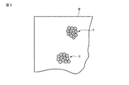
すなわち、基板Wのデバイス面には、図2に示すようにその面に露出した金属などの材料の種類によって局部的にマイナスやプラスの電荷がそれぞれマイナス電荷群X或いはプラス電荷群Yとして帯電する。そのため、デバイス面にナノバブルを含む処理液Lを供給すれば、デバイス面にマイナス或いはプラスのいずれの電荷が帯電していても、それらの電荷を確実に除去することができる。 That is, as shown in FIG. 2, negative and positive charges are locally charged on the device surface of the substrate W as a negative charge group X or a positive charge group Y depending on the type of material such as metal exposed on the surface. . Therefore, if the processing liquid L containing nanobubbles is supplied to the device surface, the charge can be reliably removed regardless of whether a negative or positive charge is charged on the device surface.
しかも、基板Wのデバイス面の電位レベルを表面電位計31で測定し、その電位レベルに応じた電子配置の気体を選択し、液体供給源17から供給される洗浄液とでナノバブルを含む処理液Lを生成するようにした。
In addition, the potential level of the device surface of the substrate W is measured by the surface potential meter 31, a gas having an electron arrangement corresponding to the potential level is selected, and the processing liquid L containing nanobubbles with the cleaning liquid supplied from the
すなわち、第1乃至第4のガス供給源15a〜15dから供給される種類の異なるそれぞれの気体は、その種類に応じて電子配置に違いがあるから、その気体の電子配置の違い応じて生成されるナノバブルがもつ帯電レベルにも差が生じる。
That is, since the different types of gases supplied from the first to fourth
したがって、表面電位計31の測定に基き、基板Wのデバイス面の帯電レベルに応じた電子配置の気体を選択すれば、ナノバブルのもつ電位レベルをデバイス面の帯電レベルとほぼ同等に設定することができる。 Therefore, based on the measurement of the surface potential meter 31, if a gas having an electronic arrangement corresponding to the charge level on the device surface of the substrate W is selected, the potential level of the nanobubbles can be set almost equal to the charge level on the device surface. it can.
それによって、基板Wのデバイス面に帯電した静電気を確実に中和して除去することができる。しかも、ナノバブルがもつ電位レベルがデバイス面の電位レベルよりも高過ぎることがないことで、ナノバブルに電荷が多く残留し、その残留した電荷が上記デバイス面に帯電して残留したり、デバイス面にナノバブルがもつ電位によって過度な衝撃を与えることもない。 Thereby, the static electricity charged on the device surface of the substrate W can be reliably neutralized and removed. In addition, since the potential level of the nanobubbles is not too high than the potential level of the device surface, a lot of charges remain in the nanobubbles, and the remaining charges remain on the device surface. There is no excessive impact by the potential of the nanobubbles.
しかも、ナノバブルがもつ電位レベルがデバイス面の電位レベルよりも低すぎることもないから、基板Wのデバイス面に帯電した電荷が残留することなく、確実に中和して除去することができる。 In addition, since the potential level of the nanobubbles is not too lower than the potential level of the device surface, the charged charges can be reliably neutralized and removed without the charged charges remaining on the device surface of the substrate W.
図4は基板Wに行う処理の種類と、基板Wの電位レベル(帯電レベル)の変化との関係を示している。すなわち、基板Wの電位レベルは、基板Wの処理内容、回転数、供給する液の種類などによって変化する。 FIG. 4 shows the relationship between the type of processing performed on the substrate W and the change in the potential level (charging level) of the substrate W. That is, the potential level of the substrate W varies depending on the processing content of the substrate W, the number of rotations, the type of liquid to be supplied, and the like.
図4に示すように処理1の場合、基板Wの電位レベルはマイナスになり、処理2の場合にはプラス、処理3の場合の電位レベルは処理1の場合よりも大きなマイナスになるなどのことがある。
As shown in FIG. 4, in the case of the process 1, the potential level of the substrate W is negative, in the case of the
したがって、処理1〜3のいずれを行うかによって変化する基板Wの帯電レベルに応じてナノバブル発生器11に供給する気体の種類を選択することで、基板Wの帯電レベルを抑制することが可能となる。 Therefore, the charge level of the substrate W can be suppressed by selecting the type of gas supplied to the nanobubble generator 11 in accordance with the charge level of the substrate W that changes depending on which of the processes 1 to 3 is performed. Become.
上記一実施の形態では基板を回転テーブルに載置して洗浄液を供給する、いわゆるスピン方式の処理装置を例に挙げて説明したが、処理槽内で基板を搬送ローラで水平搬送しながら洗浄した後、その基板から帯電した電荷を除去する場合であっても、この発明を適用することができる。 In the above-described embodiment, the substrate is placed on the rotary table and the cleaning liquid is supplied as an example, and a so-called spin processing apparatus has been described as an example, but the substrate is cleaned while being transported horizontally by the transport roller in the processing tank. Thereafter, the present invention can be applied even when the charged charge is removed from the substrate.
その場合、基板に対する洗浄液及び処理液の供給は、処理液供給ノズルに代わり、搬送される基板の搬送方向と交差する幅方向に沿って細長く形成されたスリット状のノズル孔を有する処理液供給ノズル体などを用いればよい。 In this case, the supply of the cleaning liquid and the processing liquid to the substrate is performed in place of the processing liquid supply nozzle, and the processing liquid supply nozzle having a slit-like nozzle hole that is elongated along the width direction intersecting the transport direction of the substrate to be transported. A body or the like may be used.
また、基板を洗浄処理してからそのデバイス面の電位レベルを測定し、その測定に基いて除電処理する場合について説明したが、基板の除電処理は洗浄処理の後だけに限られず、たとえば現像処理やエッチング処理など、液体を用いて基板を処理した後であれば、この発明の帯電除去を適用することができる。 In addition, although the case where the substrate surface is subjected to the cleaning process and the potential level of the device surface is measured and the charge removal process is performed based on the measurement has been described, the substrate charge removal process is not limited to the cleaning process. The charge removal according to the present invention can be applied after the substrate is processed with a liquid, such as etching or etching.
1…処理槽、2…回転テーブル、11…ナノバブル発生器(処理液供給手段)、15a〜15d…第1乃至第4のガス供給源、20…制御装置。22…処理液供給ノズル、31…表面電位計。 DESCRIPTION OF SYMBOLS 1 ... Processing tank, 2 ... Rotary table, 11 ... Nano bubble generator (processing liquid supply means), 15a-15d ... 1st thru | or 4th gas supply source, 20 ... Control apparatus. 22 ... Treatment liquid supply nozzle, 31 ... Surface potential meter.
Claims (3)
上記基板が供給される処理槽と、
上記基板の被処理面の電位レベルを検出する電位検出手段と、
この電位検出手段が検出する上記基板の被処理面の電位レベルに応じて所定の電子配置の気体を供給可能とする気体選択手段と
液体及び上記気体選択手段によって選択された気体が供給されこれら液体と気体とによって微細気泡を含む処理液を生成して上記基板の被処理面に供給する処理液供給手段と
を具備し、
上記微細気泡を含む処理液を上記基板の被処理面に供給し、上記微細気泡のもつ電荷によって上記被処理面に帯電した電荷を消失させることを特徴とする基板の帯電除去装置。 A device for removing charges charged on a substrate,
A treatment tank to which the substrate is supplied;
A potential detecting means for detecting a potential level of the surface to be processed of the substrate;
Gas selection means and liquid capable of supplying a gas having a predetermined electron arrangement according to the potential level of the surface to be processed detected by the potential detection means, and the liquid selected by the gas selection means are supplied to the liquid. And a processing liquid supply means for generating a processing liquid containing fine bubbles by gas and supplying the processing liquid to the surface to be processed of the substrate ,
An apparatus for removing charge from a substrate, comprising: supplying a treatment liquid containing the fine bubbles to a surface to be treated of the substrate; and eliminating charges charged on the surface to be treated by charges of the fine bubbles .
処理槽に基板を供給する工程と、
上記基板の被処理面の電位レベルを検出する工程と、
検出された上記被処理面の電位レベルに応じて所定の電子配置の気体を選択する工程と、
液体及び選択された上記気体によって微細気泡を含む処理液を生成して上記基板の被処理面に供給し上記微細気泡のもつ電荷によって上記被処理面に帯電した電荷を消失させる工程と
を具備したことを特徴とする基板の帯電除去方法。 A charge removal method for removing charges charged on a substrate,
Supplying a substrate to the treatment tank;
Detecting a potential level of the surface to be processed of the substrate;
Selecting a gas having a predetermined electron arrangement according to the detected potential level of the surface to be processed;
Generating a treatment liquid containing fine bubbles by the liquid and the selected gas and supplying the treatment liquid to the surface to be processed of the substrate, and erasing the charge charged on the surface to be processed by the charge of the fine bubbles. A method for removing charge from a substrate.
Priority Applications (1)
| Application Number | Priority Date | Filing Date | Title |
|---|---|---|---|
| JP2008313533A JP5408982B2 (en) | 2008-12-09 | 2008-12-09 | Substrate charge removal device and charge removal method |
Applications Claiming Priority (1)
| Application Number | Priority Date | Filing Date | Title |
|---|---|---|---|
| JP2008313533A JP5408982B2 (en) | 2008-12-09 | 2008-12-09 | Substrate charge removal device and charge removal method |
Publications (3)
| Publication Number | Publication Date |
|---|---|
| JP2010140966A JP2010140966A (en) | 2010-06-24 |
| JP2010140966A5 JP2010140966A5 (en) | 2012-01-19 |
| JP5408982B2 true JP5408982B2 (en) | 2014-02-05 |
Family
ID=42350872
Family Applications (1)
| Application Number | Title | Priority Date | Filing Date |
|---|---|---|---|
| JP2008313533A Expired - Fee Related JP5408982B2 (en) | 2008-12-09 | 2008-12-09 | Substrate charge removal device and charge removal method |
Country Status (1)
| Country | Link |
|---|---|
| JP (1) | JP5408982B2 (en) |
Families Citing this family (8)
| Publication number | Priority date | Publication date | Assignee | Title |
|---|---|---|---|---|
| EP3188849B1 (en) | 2014-09-05 | 2022-02-16 | Tennant Company | Systems and methods for supplying treatment liquids having nanobubbles |
| JP6541492B2 (en) * | 2015-07-29 | 2019-07-10 | 東京エレクトロン株式会社 | Liquid processing method and liquid processing apparatus |
| JP6924993B2 (en) * | 2017-10-04 | 2021-08-25 | 株式会社荏原製作所 | Substrate cleaning equipment and substrate cleaning method |
| KR102090975B1 (en) * | 2018-09-10 | 2020-03-19 | (주)신우에이엔티 | Wafer cleaning apparatus using nanobubble |
| JP7242228B2 (en) | 2018-09-26 | 2023-03-20 | 芝浦メカトロニクス株式会社 | SUBSTRATE PROCESSING APPARATUS AND SUBSTRATE PROCESSING METHOD |
| JP2021069999A (en) * | 2019-10-31 | 2021-05-06 | キヤノン株式会社 | Method for generating ultrafine bubble, and device and method for generating ultrafine bubble-containing liquid |
| JP7399783B2 (en) * | 2020-04-30 | 2023-12-18 | 株式会社Screenホールディングス | Substrate processing device, substrate processing method, learning data generation method, learning method, learning device, learned model generation method, and learned model |
| TW202347434A (en) * | 2022-05-26 | 2023-12-01 | 日商東京威力科創股份有限公司 | Substrate processing device and substrate processing method |
Family Cites Families (5)
| Publication number | Priority date | Publication date | Assignee | Title |
|---|---|---|---|---|
| JP2004121962A (en) * | 2002-10-01 | 2004-04-22 | National Institute Of Advanced Industrial & Technology | Method and apparatus for using nanometer-bubble |
| JP2007253120A (en) * | 2006-03-24 | 2007-10-04 | Hitachi Plant Technologies Ltd | Ultrasonic cleaning method |
| JP2007317821A (en) * | 2006-05-25 | 2007-12-06 | Dainippon Screen Mfg Co Ltd | Substrate-treating apparatus and substrate treatment method |
| JP5023705B2 (en) * | 2007-01-10 | 2012-09-12 | 東京エレクトロン株式会社 | Semiconductor device manufacturing method, semiconductor manufacturing apparatus, and storage medium |
| JP4776030B2 (en) * | 2007-03-30 | 2011-09-21 | 大日本スクリーン製造株式会社 | Substrate processing apparatus and substrate processing method |
-
2008
- 2008-12-09 JP JP2008313533A patent/JP5408982B2/en not_active Expired - Fee Related
Also Published As
| Publication number | Publication date |
|---|---|
| JP2010140966A (en) | 2010-06-24 |
Similar Documents
| Publication | Publication Date | Title |
|---|---|---|
| JP5408982B2 (en) | Substrate charge removal device and charge removal method | |
| CN108780746B (en) | Substrate cleaning apparatus, substrate cleaning method, substrate processing apparatus, and substrate drying apparatus | |
| CN109647769B (en) | Cleaning device | |
| US8888925B2 (en) | Nozzle, substrate processing apparatus, and substrate processing method | |
| JP4976949B2 (en) | Substrate processing equipment | |
| JP2012170872A (en) | Substrate cleaning apparatus, substrate cleaning method and apparatus and method for manufacturing display | |
| US20230256479A1 (en) | Substrate processing method and substrate processing device | |
| JPWO2006038472A1 (en) | Substrate processing apparatus and substrate processing method | |
| JP2006286665A (en) | Method and apparatus for cleaning electronic device | |
| JP2008183532A (en) | Substrate processing apparatus and substrate processing method | |
| KR100563843B1 (en) | Processing apparatus and processing method | |
| JPH08264626A (en) | Sample-and-hold method, method for treating fluid on sample surface, and devices for those methods | |
| WO2013035731A1 (en) | Liquid treatment apparatus for substrate, and method for controlling liquid treatment apparatus for substrate | |
| CN104971916B (en) | Cleaning device and cleaning method | |
| JP2018129470A (en) | Substrate processing apparatus and substrate processing method | |
| JP2006286947A (en) | Method and apparatus for cleaning electronic device | |
| JP2010114123A (en) | Substrate processing apparatus and method | |
| KR100682538B1 (en) | Apparatus and method for cleaning semiconductor wafer | |
| US9640384B2 (en) | Substrate cleaning apparatus and substrate cleaning method | |
| JP2009246000A (en) | Processing equipment and method of substrate | |
| JP4776030B2 (en) | Substrate processing apparatus and substrate processing method | |
| JP3638511B2 (en) | Substrate cleaning device | |
| JP2014179566A (en) | Substrate processing apparatus and substrate processing method | |
| JP5302781B2 (en) | Substrate liquid processing apparatus, substrate liquid processing method, and storage medium storing substrate liquid processing program | |
| JP2005252137A (en) | Cleaning method for substrate, and apparatus for substrate |
Legal Events
| Date | Code | Title | Description |
|---|---|---|---|
| A521 | Request for written amendment filed |
Free format text: JAPANESE INTERMEDIATE CODE: A523 Effective date: 20111128 |
|
| A621 | Written request for application examination |
Free format text: JAPANESE INTERMEDIATE CODE: A621 Effective date: 20111128 |
|
| A977 | Report on retrieval |
Free format text: JAPANESE INTERMEDIATE CODE: A971007 Effective date: 20130131 |
|
| A131 | Notification of reasons for refusal |
Free format text: JAPANESE INTERMEDIATE CODE: A131 Effective date: 20130226 |
|
| A521 | Request for written amendment filed |
Free format text: JAPANESE INTERMEDIATE CODE: A523 Effective date: 20130412 |
|
| TRDD | Decision of grant or rejection written | ||
| A01 | Written decision to grant a patent or to grant a registration (utility model) |
Free format text: JAPANESE INTERMEDIATE CODE: A01 Effective date: 20131029 |
|
| A61 | First payment of annual fees (during grant procedure) |
Free format text: JAPANESE INTERMEDIATE CODE: A61 Effective date: 20131105 |
|
| R150 | Certificate of patent or registration of utility model |
Ref document number: 5408982 Country of ref document: JP Free format text: JAPANESE INTERMEDIATE CODE: R150 |
|
| LAPS | Cancellation because of no payment of annual fees |