JP5389311B2 - Signal processing device - Google Patents
Signal processing device Download PDFInfo
- Publication number
- JP5389311B2 JP5389311B2 JP2005123270A JP2005123270A JP5389311B2 JP 5389311 B2 JP5389311 B2 JP 5389311B2 JP 2005123270 A JP2005123270 A JP 2005123270A JP 2005123270 A JP2005123270 A JP 2005123270A JP 5389311 B2 JP5389311 B2 JP 5389311B2
- Authority
- JP
- Japan
- Prior art keywords
- digital
- data
- signal
- phase difference
- output
- Prior art date
- Legal status (The legal status is an assumption and is not a legal conclusion. Google has not performed a legal analysis and makes no representation as to the accuracy of the status listed.)
- Expired - Fee Related
Links
Images


Classifications
-
- G—PHYSICS
- G01—MEASURING; TESTING
- G01R—MEASURING ELECTRIC VARIABLES; MEASURING MAGNETIC VARIABLES
- G01R19/00—Arrangements for measuring currents or voltages or for indicating presence or sign thereof
- G01R19/25—Arrangements for measuring currents or voltages or for indicating presence or sign thereof using digital measurement techniques
- G01R19/2506—Arrangements for conditioning or analysing measured signals, e.g. for indicating peak values ; Details concerning sampling, digitizing or waveform capturing
-
- H—ELECTRICITY
- H03—ELECTRONIC CIRCUITRY
- H03H—IMPEDANCE NETWORKS, e.g. RESONANT CIRCUITS; RESONATORS
- H03H21/00—Adaptive networks
- H03H21/0012—Digital adaptive filters
-
- G—PHYSICS
- G01—MEASURING; TESTING
- G01R—MEASURING ELECTRIC VARIABLES; MEASURING MAGNETIC VARIABLES
- G01R25/00—Arrangements for measuring phase angle between a voltage and a current or between voltages or currents
Description
本願発明は、入力される2つの交流信号を所定のディジタル信号処理を行って2つの交流信号の位相差を算出する信号処理装置に関するものである。 The present invention relates to a signal processing device that performs predetermined digital signal processing on two input AC signals to calculate a phase difference between the two AC signals.
互いに位相の異なる2つの交流信号をV(θ)=sin(θ)、I(θ)=sin(θ−φ)(θ=ωt,ωは角速度、φは位相差)とすると、位相差φの関数sin(φ),cos(φ)は、三角関数の公式より、下記に示す(7)式と(8)式とによって求めることができる。なお、(7)式,(8)式において、V’(θ)、I’(θ)はそれぞれV(θ)、I(θ)の微分関数である。 Assuming that two AC signals having different phases are V (θ) = sin (θ), I (θ) = sin (θ−φ) (θ = ωt, ω is an angular velocity, φ is a phase difference), the phase difference φ The functions sin (φ) and cos (φ) can be obtained by the following formulas (7) and (8) from the trigonometric formula. In the equations (7) and (8), V ′ (θ) and I ′ (θ) are differential functions of V (θ) and I (θ), respectively.

従来、ディジタル信号処理により上記の(7)式及び(8)式の演算処理を行うことにより、位相差φを算出する信号処理装置が知られている(例えば、特許文献1参照)。 2. Description of the Related Art Conventionally, a signal processing apparatus that calculates a phase difference φ by performing arithmetic processing of the above formulas (7) and (8) by digital signal processing is known (for example, see Patent Document 1).
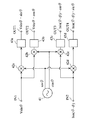
従来の信号処理回路は、図7に示す演算回路を有し、同図に示す演算回路から出力される4つの演算結果Vsin(θ)・sin(θ),Vsin(θ)・cos(θ),Isin(θ−φ)・cos(θ),Isin(θ−φ)・sin(θ)を用いて、(7)式及び(8)式内の各項を演算することにより、関数cos(φ),sin(φ)やこれらの関数から更にtan-1(φ)を演算して位相差φを算出している。 The conventional signal processing circuit has an arithmetic circuit shown in FIG. 7, and four arithmetic results Vsin (θ) · sin (θ) and Vsin (θ) · cos (θ) output from the arithmetic circuit shown in FIG. , Isin (θ−φ) · cos (θ), Isin (θ−φ) · sin (θ), and by calculating each term in the equations ( 7 ) and ( 8 ), the function cos ( The phase difference φ is calculated by further calculating tan −1 (φ) from φ), sin (φ) and these functions.
なお、図7に示す演算回路は、2つの基準波sin(θ),cos(θ)を出力する発振部41と、発振部41から出力される基準波sin(θ),cos(θ)と、入力信号である2つの交流信号Vsin(θ),Isin(θ−φ)とを乗算する乗算部42a,42b,42c,42dと、高調波を除去するためのディジタルローパスフィルタ43a,43b,43c,43dとを備えている。
Note that the arithmetic circuit shown in FIG. 7 includes an
この構成によると、発振部41から出力された基準波sin(θ)は、乗算部42aにおいて、入力された交流電圧信号Vsin(θ)と乗算され、その演算結果の信号Vsin(θ)・sin(θ)がディジタルローパスフィルタ43aを介して出力される。また、基準波sin(θ)は、乗算部42dにおいて、入力された交流電流信号Isin(θ−φ)と乗算され、その演算結果の信号Isin(θ−φ)・sin(θ)がディジタルローパスフィルタ43dを介して出力される。
According to this configuration, the reference wave sin (θ) output from the oscillating
一般に乗算部42aに入力される基準波sin(θ)と交流電圧信号Vsin(θ)の周波数とは正確には一致しない。交流電圧信号と基準波との微小な周波数のずれをΔωとし、基準波をsin(ωt+Δωt)、cos(ωt+Δωt)とすると、乗算部42aから出力される信号は、Vsin(ωt)・sin(ωt+Δωt)となり、乗算部42dから出力される信号は、Isin(ωt−φ)・sin(ωt+Δωt)となる。
Generally, the frequency of the reference wave sin (θ) and the AC voltage signal Vsin (θ) input to the
これらの出力信号を三角関数の積和の公式により変形すると、Vsin(ωt)・sin(ωt+Δωt)=(V/2)・[sin(2ωt+Δωt)+cos(Δωt)]、Isin(ωt−φ)・sin(ωt+Δωt)=(I/2)・[sin(2ωt+Δωt−φ)+cos(Δωt+φ)]、となり、乗算部42aの出力信号に基準波の2次高調波sin(2ωt)が含まれることになるので、これを除去するため、乗算部42aの後段にディジタルローパスフィルタ43aが設けられ、乗算部42dの後段にディジタルローパスフィルタ43dが設けられている。
When these output signals are transformed by a product-sum formula of trigonometric functions, Vsin (ωt) · sin (ωt + Δωt) = (V / 2) · [sin (2ωt + Δωt) + cos (Δωt)], Isin (ωt−φ) · sin (ωt + Δωt) = (I / 2) · [sin (2ωt + Δωt−φ) + cos (Δωt + φ)], and the output signal of the
従って、演算回路の出力端OUT1,OUT4からはそれぞれ基準波の2次高調波を含まないVsin(θ)・sin(θ)とIsin(θ−φ)・sin(θ)とが出力される。
Therefore, the Vsin without the output OUT1,
また、発振部41から出力された基準波cos(θ)は、乗算部42bにおいて、交流電圧信号Vsin(θ)と乗算され、その演算結果の信号Vsin(θ)・cos(θ)がディジタルローパスフィルタ43bを介して出力されるとともに、乗算部42cにおいて、交流電流信号Isin(θ−φ)と乗算され、その演算結果の信号Isin(θ−φ)・cos(θ)がディジタルローパスフィルタ43cを介して出力される。
The reference wave cos (θ) output from the oscillating
乗算器42b,42cについても乗算器42a,42dと同様にその出力信号には基準波の2次高調波が含まれるので、乗算器42bと乗算器42cの後段にそれぞれディジタルローパスフィルタ43bとディジタルローパスフィルタ43cが設けられている。すなわち、乗算器42b,42cの出力信号は、Isin(ωt)・cos(ωt+Δωt)=(V2)・[sin(2ωt+Δωt−φ)+sin(Δωt)]、Isin(ωt−φ)・cos(ωt+Δωt)=(I/2)・[sin(2ωt+Δωt−φ)+sin(Δωt+φ)]となり、それぞれ基準波の2次高調波sin(2ωt)が含まれることになるので、その2次高調波sin(2ωt)はディジタルローパスフィルタ43b,43cによって除去される。
Similarly to the
ところで、上記位相差演算回路では、発振部41から出力される基準波sin(θ),cos(θ)と、入力される交流電圧信号Vsin(θ),交流電流信号Isin(θ−φ)との周波数の微小誤差によって出力端OUT1〜OUT4から出力される4個の出力値が大きく影響を受け、その結果、(7)式及び(8)式によって算出される位相差φに関する値を正確に演算することができず、位相差φの検出精度が不安定であるといった問題点を有する。
In the phase difference calculation circuit, the reference waves sin (θ) and cos (θ) output from the oscillating
また、乗算部42a〜42dの後段に基準波の2次高調波を除去するためのディジタルローパスフィルタ43a〜43dを必要とするので、これらのディジタルローパスフィルタ43a〜43dでのフィルタリング処理に時間を要し、位相差演算回路全体の演算速度の高速化が困難であるといった問題点もあった。
Further, since digital low-
本願発明は、上記した事情のもとで考え出されたものであって、2つの交流信号の位相差を高速にかつ高精度で算出することのできる信号処理装置を提供することを、その課題とする。 The present invention has been conceived under the circumstances described above, and its object is to provide a signal processing device capable of calculating the phase difference between two AC signals at high speed and with high accuracy. And
上記の課題を解決するため、本願発明では、次の技術的手段を講じている。 In order to solve the above problems, the present invention takes the following technical means.
本願発明によって提供される信号処理装置は、入力される2つのアナログの交流信号を所定のディジタル信号処理を行って2つの交流信号の位相差を算出する信号処理装置であって、前記2つの交流信号をそれぞれ予め設定された所定の周期でサンプリングし、各サンプリングのレベル値を示すディジタル交流データに変換する信号変換手段と、フィードバックによって通過帯域の共振周波数を所望の周波数に追従させる適応型ディジタルフィルタを有し、前記信号変換手段から出力される2つのディジタル交流データから前記共振周波数のディジタル交流データx[k],y[k]をそれぞれ濾波して出力し、併せて、前記共振周波数に基づく余弦信号データを出力する濾波手段と、前記濾波手段から出力されるディジタル交流データx[k],y[k]と前記余弦信号データとを用いて下記(1)〜(4)式により前記ディジタル交流データx[k],y[k]を微分した2つのディジタル交流データx’[k],y’[k]を演算する微分演算手段と、前記濾波手段から出力される2つのディジタル交流データx[k],y[k]と、前記微分演算手段から出力される2つのディジタル交流データx’ [k],y’ [k]を用いて、下記(5),(6)式により前記2つのディジタル交流データx[k],y[k]の位相差φを演算する位相差演算手段と、を備えることを特徴としている(請求項1)。 The signal processing apparatus provided by the present invention is a signal processing apparatus that performs predetermined digital signal processing on two input analog AC signals and calculates a phase difference between the two AC signals, and the two AC signals Signal conversion means for sampling a signal at a predetermined cycle and converting it into digital AC data indicating the level value of each sampling, and an adaptive digital filter for tracking the resonance frequency of the passband to a desired frequency by feedback And filtering and outputting the digital AC data x [k] and y [k] of the resonance frequency from the two digital AC data output from the signal conversion means, and based on the resonance frequency. Filtering means for outputting cosine signal data and digital AC data x [k], y [output from the filtering means. Two digital AC data x ′ [k], y ′ obtained by differentiating the digital AC data x [k], y [k] by the following equations (1) to (4) using k] and the cosine signal data. differential arithmetic means for calculating [k], two digital AC data x [k], y [k] output from the filtering means, and two digital AC data x ′ [2] output from the differential arithmetic means. a phase difference calculating means for calculating a phase difference φ between the two digital AC data x [k] and y [k] using the following equations (5) and (6) using k] and y ′ [k]: (Claim 1).
ここで、「A1」,「A2」は各交流信号の振幅値を示す。また、「ω」は角周波数を示し、「k+1」は、信号変換手段によるサンプリングデータの時間軸上の位置kに対して1つ後の時間軸上の位置を示し、「k−1」は、上記kに対して1つ前の時間軸上の位置を示す。 Here, “A 1 ” and “A 2 ” indicate the amplitude value of each AC signal. “Ω” indicates an angular frequency, “k + 1” indicates a position on the time axis that is one after the position k on the time axis of the sampling data by the signal conversion means, and “k−1” indicates , The position on the time axis immediately before k is shown.
この構成によれば、濾波手段から出力される2つのディジタル交流データx[k],y[k]と、微分演算手段から出力される2つのディジタル交流データx’ [k],y’ [k]を用いて位相差演算手段によって入力される交流信号の位相差を正確に求めることができる。そのため、従来のように、基準波を発生させて位相差を求めていた構成に比して、検出精度をはるかに向上させることができる。また、高調波を除去するためのディジタルローパスフィルタを用いる必要がないため、高速に位相差を演算することができる。また、発振部やディジタルローパスフィルタ等を用いる必要がない結果、回路構成が容易となる。 According to this configuration, the two digital AC data x [k], y [k] output from the filtering means and the two digital AC data x ′ [k], y ′ [k] output from the differential operation means. ] Can be used to accurately determine the phase difference of the AC signal input by the phase difference calculation means. Therefore, the detection accuracy can be greatly improved as compared with the conventional configuration in which a reference wave is generated to obtain a phase difference. Further, since it is not necessary to use a digital low-pass filter for removing harmonics, the phase difference can be calculated at high speed. In addition, as a result of not having to use an oscillation unit, a digital low-pass filter, or the like, the circuit configuration is facilitated.
また、上記信号処理装置において、前記信号変換手段によって2つの交流信号を変換する前に、当該2つの交流信号を所定の増幅度で増幅する増幅手段をさらに備えるとよい(請求項2) The signal processing apparatus may further include an amplifying unit that amplifies the two AC signals at a predetermined amplification degree before the two AC signals are converted by the signal converting unit.
本願発明のその他の特徴および利点は、添付図面を参照して以下に行う詳細な説明によって、より明らかとなろう。 Other features and advantages of the present invention will become more apparent from the detailed description given below with reference to the accompanying drawings.
以下、本願発明の好ましい実施の形態を、添付図面を参照して具体的に説明する。 Hereinafter, preferred embodiments of the present invention will be specifically described with reference to the accompanying drawings.
図1は、本願発明に係る信号処理装置が適用される高周波電力供給システムの一例を示す図である。この高周波電力供給システムは、半導体ウェハや液晶基板等の被加工物に対して高周波電力を供給して、例えばプラズマエッチングといった加工処理を行うものである。この高周波電力供給システムは、高周波電源装置1、インピーダンス整合装置2及び負荷としてのプラズマチャンバー3で構成され、インピーダンス整合装置2とプラズマチャンバー3との間には、プラズマチャンバー3の入力端における高周波の電圧信号と電流信号とを測定する電圧/電流測定装置4が設けられ、この電圧/電流測定装置4に本実施形態に係る信号処理装置が適用される。
FIG. 1 is a diagram showing an example of a high-frequency power supply system to which a signal processing apparatus according to the present invention is applied. This high-frequency power supply system supplies high-frequency power to a workpiece such as a semiconductor wafer or a liquid crystal substrate, and performs processing such as plasma etching. The high-frequency power supply system includes a high-frequency
電圧/電流測定装置4は、図2に示すように、主としてアナログの交流電圧信号を検出する電圧検出部11aと、アナログの交流電流信号を検出する電流検出部11bとからなるアナログ信号処理部11と、このアナログ信号処理部11から出力されるアナログ信号(交流電圧信号と交流電流信号)をディジタル信号に変換して交流電圧信号の実効値Vrms、交流電流信号の実効値Irms、及び交流電圧信号と交流電流信号の位相差φを算出するディジタル信号処理部12とで構成されている。
As shown in FIG. 2, the voltage /
ディジタル信号処理部12は、図3に示すように、アナログ信号処理部11から入力される交流信号を所定の増幅度で増幅するゲイン調整回路21a,21b、ゲイン調整回路21a,21bから入力されるアナログ信号をディジタル信号に変換するA/D変換部22、A/D変換部22から出力されるディジタルの交流信号から所望の周波数の交流信号を抽出するディジタルフィルタ部23、交流電圧信号の実効値Vrmsを演算する実効値演算回路24、交流電流信号の実効値Irmsを演算する実効値演算回路25、及び交流電圧信号と交流電流信号との間の位相差φを演算する位相差演算回路26により構成されている。
As shown in FIG. 3, the digital
ゲイン調整回路21aは、アナログ信号処理部11の電圧検出部11aで検出された交流電圧信号Vを増幅するものであり、ゲイン調整回路21bは、アナログ信号処理部11の電流検出部11bで検出された交流電流信号Iを増幅するものである。なお、ゲイン調整回路21a,21bは、アナログ信号処理部11に含まれていてもよい。
The
電圧/電流測定装置4では、入力される交流信号がディジタル処理されるため、交流信号の入力レベルが小さいと、ディジタル処理における演算の精度が悪化することがある。そのため、本実施形態では、ゲイン調整回路21a,21bを設けることにより、低いレベルの交流信号が入力されても安定したディジタル処理を行い得るようにしている。
In the voltage /
A/D変換部22は、交流電圧信号に対するA/D変換回路22aと交流電流信号に対するA/D変換回路22bを有している。また、ディジタルフィルタ部23は、交流電圧信号に対して所望の周波数の交流電圧信号を抽出するための適応型ディジタルフィルタ23aと、交流電流信号に対して所望の周波数の交流電流信号を抽出するための適応型ディジタルフィルタ23bとを有している。ここに所望の周波数とは、高周波電源装置1から出力される高周波電源の周波数で、例えば高周波電力供給システムに使用される13.56Hzの周波数である。
The A /
また、適応型ディジタルフィルタ23a,23bは、いわゆるIIR(infinite impulse response)ローパスフィルタからなり、入力されるディジタルの交流信号データのうち、所定の遮断周波数以上の周波数成分を除去するものであって、例えば図4に示す構成の、共振周波数foを所望の周波数に追従させることのできるディジタルフィルタである。適応型ディジタルフィルタ23aからは、交流電圧信号データ及び余弦信号データが出力され、適応型ディジタルフィルタ23bからは、交流電流信号データが出力される。
The adaptive
例えば、適応型ディジタルフィルタ23a,23bは、IIRローパスフィルタからなるディジタルフィルタ31とこのディジタルフィルタ31の通過帯域の中心周波数を決定する係数aを制御する係数制御回路32とで構成され、ディジタルフィルタ31にディジタルデータ(サンプリングデータ)r[n]が入力される毎に、当該ディジタルデータのレベル値r[n]とディジタルフィルタ31から出力されるディジタルデータのレベル値x[n]との誤差e[n]=r[n]−x[n]が最小となるように係数a[n+1]を演算し、その演算結果を次のディジタルデータr[n+1]の入力の際にディジタルフィルタ31に設定することにより、ディジタルフィルタ31に入力される信号のうち、特定の単一周波数foの信号のみを濾波するものである。なお、係数aは、周波数との関係においてa=2r・cos(ω)が成立し、この係数aは、係数信号データとして位相差演算回路26に出力される。ここで、rは極座標で表したときの極半径を示す。
For example, adaptive
位相差演算回路26は、適応型ディジタルフィルタ23a,23bから出力される交流電圧信号データ、交流電流信号データ及び係数信号データから両交流信号の位相差を演算により求めるものである。
The phase
図5は、位相差演算回路26のブロック構成図である。位相差演算回路26は、2つの微分演算回路33,34と、算出演算回路35と、数式演算回路36とによって構成されている。
FIG. 5 is a block configuration diagram of the phase
微分演算回路33は、交流電圧信号データx[k]を微分して交流電圧信号データx′[k]を出力するものである。微分演算回路34は、交流電流信号データy[k]を微分して交流電流信号データy′[k]を出力するものである。算出演算回路35は、入力される係数信号データである係数aに基づいて1/[2sin(ω) ]を演算により求め、その値を各微分演算回路33,34に出力するものである。数式演算回路36は、微分演算回路33,34からの交流電圧信号データx′[k]及び交流電流信号データy′[k]に基づいて、下記に示す(13)、(14)式を演算するものである。
The
この構成によれば、微分演算回路33,34には、下式に示す交流電圧信号データx[k]及び交流電流信号データy[k]が入力される。
According to this configuration, the AC voltage signal data x [k] and the AC current signal data y [k] represented by the following expressions are input to the
ここで、A1は交流電圧信号の振幅値であり、A2は交流電流信号の振幅値である。また、「ω」は角周波数であり、「k」はA/D変換部22によるサンプリングデータの時間軸上の位置を示す。
Here, A 1 is the amplitude value of the AC voltage signal, and A 2 is the amplitude value of the AC current signal. “Ω” is an angular frequency, and “k” indicates a position on the time axis of sampling data by the A /
次いで、微分演算回路33,34では、交流電圧信号データx[k]及び交流電流信号データy[k]に基づいて各交流信号データにおける直交成分x′[k],y′[k]が以下の演算式(11)、(12)により求められる。このとき、算出演算回路35においては、上述した係数a=2r・cos(ω)に基づいて、cos(ω)がcos(ω)=a/2rの演算式によって求められる。そして、このcos(ω)に基づいて1/[2sin(ω) ]の値が演算により求められ、その値が各微分演算回路33,34に出力される。すなわち、sin(ω)は、√[1−cos2(ω)]によって算出することができる。
Next, in the
ここで、「k+1」は、図6に示すように、A/D変換部22によるサンプリングデータの時間軸上の位置kに対して1つ後の時間軸上の位置を示し、「k−1」は、上記kに対して1つ前の時間軸上の位置を示す。
Here, “k + 1” indicates a position on the time axis that is one after the position k on the time axis of the sampling data by the A /
そして、各交流信号データにおける直交成分x′[k],y′[k]は、数式演算回路36に入力され、下記に示す演算式(13)、(14)に基づく演算が行われることにより、cos(φ),sin(φ)の位相差データp[k],q[k]がそれぞれ求められる。このようにして、位相差φが求められる。なお、数式演算回路36は、tan(φ)を出力するようにして、tan(φ)から位相差φを求めるようにしてもよい。
Then, the orthogonal components x ′ [k], y ′ [k] in each AC signal data are input to the mathematical
なお、cos(φ),sin(φ)は、以下のようにして求められる。ここでは、アナログ信号として正弦波x(θ),y(θ)を考えると、x(θ),y(θ)は以下の(15)、(16)式で表される。 Note that cos (φ) and sin (φ) are obtained as follows. Here, considering sine waves x (θ) and y (θ) as analog signals, x (θ) and y (θ) are expressed by the following equations (15) and (16).
ここで、x(θ),y(θ)を微分した値x′(θ),y′(θ)は、は、それぞれ以下の(17)、(18)式で表される。 Here, values x ′ (θ) and y ′ (θ) obtained by differentiating x (θ) and y (θ) are expressed by the following equations (17) and (18), respectively.
また、α=θ、β=θ−φとすると、α−β=φとなる。そのため、sin(φ) ,cos(φ) は、それぞれ以下の(19)、(20)式で表される。 If α = θ and β = θ−φ, then α−β = φ. Therefore, sin (φ) and cos (φ) are expressed by the following equations (19) and (20), respectively.
そして、(15)〜(18)式を変形してそれぞれ(19)式、(20)式に代入すると、sin(φ) ,cos(φ) は、それぞれ以下の(21)、(22)式で表される。 When the equations (15) to (18) are modified and substituted into the equations (19) and (20), sin (φ) and cos (φ) are expressed by the following equations (21) and (22), respectively. It is represented by
このように、位相差演算回路26では、入力される交流電圧信号及び交流電流信号がディジタル処理され、上記した演算式を用いて交流電圧信号と交流電流信号との位相差φを求めることができるので、位相差φを正確にかつ高速に求めることができる。そのため、従来のように、基準波を発生させて位相差を求めていた構成に比して、検出精度をはるかに向上させることができる。また、高調波を除去するためのディジタルローパスフィルタを用いる必要がないため、高速に位相差を演算することができる。また、位相差演算回路26において、発振部やディジタルローパスフィルタ等を用いる必要がない結果、回路構成が容易となる。
Thus, in the phase
図2に示す電圧/電流測定装置4によれば、アナログ信号処理部11の電圧検出部11aによりプラズマチャンバー3の入力端における高周波電源の交流電圧信号が検出され、所定のアナログ信号処理(不要なノイズを除去するフィルタリング処理等)が行われた後、ディジタル信号処理部12に入力される。ディジタル信号処理部12では、ゲイン調整回路21aによりレベル調整が行われ、A/D変換回路22aによりアナログの電圧信号がディジタルの電圧信号(サンプリングデータ)に変換された後、適応型ディジタルフィルタ23aで所望の周波数(この例では、13.56MHz)の電圧信号が抽出され、その電圧信号が実効値演算回路24と位相差演算回路26に入力される。
According to the voltage /
また、アナログ信号処理部11の電流検出部11bによりプラズマチャンバー3の入力端における高周波電源の交流電流信号が検出され、上述と同様の所定のアナログ信号処理が行われた後、ディジタル信号処理部12に入力される。ディジタル信号処理部12では、ゲイン調整回路21bによりレベル調整が行われ、A/D変換回路22bによりアナログの電流信号がディジタルの電流信号(サンプリングデータ)に変換された後、適応型ディジタルフィルタ23bで所望の周波数(この例では、13.56MHz)の電流信号のみが抽出され、その電流信号が実効値演算回路25と位相差演算回路26に入力される。
In addition, after the
そして、実効値演算回路24で、上述したディジタル信号処理により周波数13.56MHzの交流電圧信号Vの実効値Vrmsを示すディジタルデータが生成され、外部に出力される。同様に実効値演算回路25で、上述したディジタル信号処理により周波数13.56MHzの交流電流信号Iの実効値Irmsを示すディジタルデータが生成され、外部に出力される。また、位相差演算回路26により交流電圧信号Vと交流電流信号Iとの位相差φが演算され、その演算値を示すディジタルデータが生成され、外部に出力される。
Then, the effective
もちろん、この発明の範囲は上述した実施の形態に限定されるものではない。 Of course, the scope of the present invention is not limited to the embodiment described above.
1 高周波電源装置
2 インピーダンス整合装置
3 プラズマチャンバー
4 電圧/電流測定装置
11 アナログ信号処理部
12 ディジタル信号処理部
21a,21b ゲイン調整回路
22 A/D変換部
23 ディジタルフィルタ部
26 位相差演算回路
DESCRIPTION OF
Claims (2)
前記2つの交流信号をそれぞれ予め設定された所定の周期でサンプリングし、各サンプリングのレベル値を示すディジタル交流データに変換する信号変換手段と、
フィードバックによって通過帯域の共振周波数を所望の周波数に追従させる適応型ディジタルフィルタを有し、前記信号変換手段から出力される2つのディジタル交流データから前記共振周波数のディジタル交流データx[k],y[k]をそれぞれ濾波して出力し、併せて、前記共振周波数に基づく余弦信号データを出力する濾波手段と、
前記濾波手段から出力されるディジタル交流データx[k],y[k]と前記余弦信号データとを用いて下記(1)〜(4)式により前記ディジタル交流データx[k],y[k]を微分した2つのディジタル交流データx’[k],y’[k]を演算する微分演算手段と、
前記濾波手段から出力される2つのディジタル交流データx[k],y[k]と、前記微分演算手段から出力される2つのディジタル交流データx’[k],y’[k]を用いて、下記(5),(6)式により前記2つのディジタル交流データx[k],y[k]の位相差φを演算する位相差演算手段と、
を備えることを特徴とする、信号処理装置。
A signal conversion means for sampling the two AC signals at a predetermined cycle, respectively, and converting the sampling signals into digital AC data indicating the level value of each sampling;
It has an adaptive digital filter that makes the resonance frequency of the passband follow a desired frequency by feedback, and from the two digital AC data output from the signal conversion means, the digital AC data x [k], y [ k] for filtering and outputting, respectively, and filtering means for outputting cosine signal data based on the resonance frequency;
Using the digital AC data x [k] and y [k] output from the filtering means and the cosine signal data , the digital AC data x [k] and y [k] are expressed by the following equations (1) to (4). Differential operation means for calculating two digital AC data x ′ [k] and y ′ [k] obtained by differentiating
Using the two digital AC data x [k], y [k] output from the filtering means and the two digital AC data x ′ [k], y ′ [k] output from the differential operation means Phase difference calculating means for calculating a phase difference φ between the two digital AC data x [k] and y [k] according to the following equations (5) and (6):
A signal processing apparatus comprising:
Priority Applications (2)
| Application Number | Priority Date | Filing Date | Title |
|---|---|---|---|
| JP2005123270A JP5389311B2 (en) | 2005-04-21 | 2005-04-21 | Signal processing device |
| US11/406,885 US7702702B2 (en) | 2005-04-21 | 2006-04-19 | Signal processing device for computing phase difference between alternating current signals |
Applications Claiming Priority (1)
| Application Number | Priority Date | Filing Date | Title |
|---|---|---|---|
| JP2005123270A JP5389311B2 (en) | 2005-04-21 | 2005-04-21 | Signal processing device |
Publications (3)
| Publication Number | Publication Date |
|---|---|
| JP2006300746A JP2006300746A (en) | 2006-11-02 |
| JP2006300746A5 JP2006300746A5 (en) | 2010-02-25 |
| JP5389311B2 true JP5389311B2 (en) | 2014-01-15 |
Family
ID=37235708
Family Applications (1)
| Application Number | Title | Priority Date | Filing Date |
|---|---|---|---|
| JP2005123270A Expired - Fee Related JP5389311B2 (en) | 2005-04-21 | 2005-04-21 | Signal processing device |
Country Status (2)
| Country | Link |
|---|---|
| US (1) | US7702702B2 (en) |
| JP (1) | JP5389311B2 (en) |
Families Citing this family (16)
| Publication number | Priority date | Publication date | Assignee | Title |
|---|---|---|---|---|
| US8603736B2 (en) | 2004-06-07 | 2013-12-10 | Monogram Biosciences, Inc. | Compositions and methods for determining resistance to inhibitors of virus entry using recombinant virus assays |
| JP5255930B2 (en) * | 2008-07-04 | 2013-08-07 | 新電元工業株式会社 | Phase detector |
| US7825719B2 (en) * | 2008-12-29 | 2010-11-02 | Advanced Energy Industries, Inc. | System and method for wideband phase-adjustable common excitation |
| JP5371052B2 (en) * | 2010-03-31 | 2013-12-18 | 株式会社ダイヘン | High frequency power supply |
| JP5392166B2 (en) * | 2010-04-02 | 2014-01-22 | トヨタ自動車株式会社 | Fuel cell system |
| JP2013250231A (en) * | 2012-06-04 | 2013-12-12 | Daihen Corp | Phase difference detection device, phase difference detection program, and plasma processing system using phase difference detection device |
| EP2936541B1 (en) | 2012-12-18 | 2017-02-01 | TRUMPF Hüttinger GmbH + Co. KG | Method for producing high-frequency power and power supply system having a power converter for supplying a load with power |
| EP2936542B1 (en) | 2012-12-18 | 2018-02-28 | TRUMPF Hüttinger GmbH + Co. KG | Arc extinguishing method and power supply system having a power converter |
| US9609653B2 (en) * | 2014-10-15 | 2017-03-28 | National Instruments Corporation | Spectral stitching method to increase instantaneous bandwidth in vector signal generators |
| JP5971425B1 (en) | 2015-03-16 | 2016-08-17 | 純教 西江 | AC signal analyzing apparatus, AC signal analyzing method and program |
| JP6195393B1 (en) * | 2016-03-23 | 2017-09-13 | ウィンボンド エレクトロニクス コーポレーション | Output circuit |
| CN109856929B (en) * | 2017-11-30 | 2020-06-16 | 上海微电子装备(集团)股份有限公司 | Signal processing device and processing method, alignment system and alignment method and photoetching machine |
| CN113740594B (en) * | 2021-09-10 | 2023-10-17 | 温州大学 | High-precision measuring circuit for effective value of alternating voltage |
| CN113740591B (en) * | 2021-09-10 | 2023-10-13 | 温州大学 | Optimal estimation method for effective value of periodic signal |
| CN113740592B (en) * | 2021-09-13 | 2023-10-13 | 温州大学 | Optimal measurement circuit for effective value of periodic signal |
| US20240039563A1 (en) * | 2022-07-26 | 2024-02-01 | Bae Systems Information And Electronic Systems Integration Inc. | Method for rapid baseline recovery for irregular frequency content large dynamic range unipolar data signals |
Family Cites Families (15)
| Publication number | Priority date | Publication date | Assignee | Title |
|---|---|---|---|---|
| US5165051A (en) * | 1990-05-15 | 1992-11-17 | The United States Of America As Represented By The Administrator Of The National Aeronautics And Space Administration | Modified fast frequency acquisition via adaptive least squares algorithm |
| US5117726A (en) * | 1990-11-01 | 1992-06-02 | International Business Machines Corporation | Method and apparatus for dynamic midi synthesizer filter control |
| EP0526836B1 (en) * | 1991-08-07 | 1997-01-29 | Kabushiki Kaisha Toshiba | QPSK demodulator with automatic frequency control |
| JPH06188683A (en) * | 1992-04-23 | 1994-07-08 | Masatada Hata | Adaptive digital filter |
| JPH0645832A (en) * | 1992-07-24 | 1994-02-18 | Olympus Optical Co Ltd | Digital phase discriminating method |
| JP3144283B2 (en) * | 1995-10-24 | 2001-03-12 | 松下電器産業株式会社 | Delay detector |
| JP3252694B2 (en) * | 1996-02-26 | 2002-02-04 | 富士電機株式会社 | Phase difference measuring device |
| US5949821A (en) * | 1996-08-05 | 1999-09-07 | Motorola, Inc. | Method and apparatus for correcting phase and gain imbalance between in-phase (I) and quadrature (Q) components of a received signal based on a determination of peak amplitudes |
| JP3256661B2 (en) * | 1996-09-18 | 2002-02-12 | 三菱電機株式会社 | AC amplitude detector |
| JPH11287830A (en) * | 1998-04-01 | 1999-10-19 | Kawasaki Steel Corp | Detection method and device of phase component of sign wave signal |
| JPH11308075A (en) * | 1998-04-22 | 1999-11-05 | Kokusai Electric Co Ltd | Digital filter circuit |
| JP2000338141A (en) * | 1999-03-25 | 2000-12-08 | Tokyo Electric Power Co Inc:The | Apparatus and method for measuring voltage and apparatus and method for measuring electric energy |
| US6657394B2 (en) | 2001-04-06 | 2003-12-02 | Eni Technology, Inc. | Reflection coefficient phase detector |
| JP2004096871A (en) * | 2002-08-30 | 2004-03-25 | Hitachi Ltd | Linkage protection system for distributed power supply equipment |
| JP2004214963A (en) * | 2002-12-27 | 2004-07-29 | Sony Corp | Ofdm demodulator |
-
2005
- 2005-04-21 JP JP2005123270A patent/JP5389311B2/en not_active Expired - Fee Related
-
2006
- 2006-04-19 US US11/406,885 patent/US7702702B2/en not_active Expired - Fee Related
Also Published As
| Publication number | Publication date |
|---|---|
| US20060248138A1 (en) | 2006-11-02 |
| JP2006300746A (en) | 2006-11-02 |
| US7702702B2 (en) | 2010-04-20 |
Similar Documents
| Publication | Publication Date | Title |
|---|---|---|
| JP5389311B2 (en) | Signal processing device | |
| JP5631628B2 (en) | Multi-rate processing for plasma RF source measurement | |
| US8841902B2 (en) | Testing device and testing method for non destructive detection of a defect in a test piece by means of an eddy current | |
| JP4436884B1 (en) | Signal processing method, signal processing apparatus, and Coriolis flow meter | |
| JP2008527378A (en) | Method for detecting RF power supplied to a load and complex impedance of the load | |
| JP2003337062A (en) | Noise eliminator for gravimetry and noise elimination method for gravimetry | |
| WO2011102031A1 (en) | Signal processing method, signal processing device, and coriolis flow meter. | |
| JP2007033286A (en) | Method and device for measuring impedance | |
| JP2014126523A (en) | Speed calculation device, speed calculation method, and program | |
| EP1164355B1 (en) | Angular velocity sensor | |
| EP2618140A2 (en) | Test Set-Up and Test Method for Non-Destructive Detection of a Flaw in a Device under Test by Means of an Eddy Current | |
| JP2002329599A (en) | Device for detecting phase and supplying power | |
| JP2005344874A (en) | Magnetic bearing device | |
| US20050171992A1 (en) | Signal processing apparatus, and voltage or current measurer utilizing the same | |
| JP2010181307A (en) | Signal processing method and apparatus, and coriolis flowmeter | |
| EP2363693A1 (en) | Signal processing method, signal processing apparatus, and coriolis flowmeter | |
| JP4002132B2 (en) | Electromagnetic flow meter | |
| JP2005214932A5 (en) | ||
| JP5070787B2 (en) | Surface acoustic wave measuring apparatus and method | |
| JP2008170412A (en) | Signal processing method and signal processor | |
| JP2008128856A (en) | Measuring device using spherical surface acoustic wave device | |
| US7038605B2 (en) | Apparatus and method for measuring noise, and recording medium | |
| CN114152296A (en) | FPGA-based electromagnetic water meter signal processing method | |
| JP2014199737A (en) | High frequency power supply device | |
| JPH08136596A (en) | Phase-difference measuring apparatus |
Legal Events
| Date | Code | Title | Description |
|---|---|---|---|
| A521 | Request for written amendment filed |
Free format text: JAPANESE INTERMEDIATE CODE: A523 Effective date: 20080410 |
|
| A621 | Written request for application examination |
Free format text: JAPANESE INTERMEDIATE CODE: A621 Effective date: 20080410 |
|
| A521 | Request for written amendment filed |
Free format text: JAPANESE INTERMEDIATE CODE: A523 Effective date: 20100113 |
|
| A131 | Notification of reasons for refusal |
Free format text: JAPANESE INTERMEDIATE CODE: A131 Effective date: 20110614 |
|
| A521 | Request for written amendment filed |
Free format text: JAPANESE INTERMEDIATE CODE: A523 Effective date: 20110803 |
|
| A131 | Notification of reasons for refusal |
Free format text: JAPANESE INTERMEDIATE CODE: A131 Effective date: 20120403 |
|
| A521 | Request for written amendment filed |
Free format text: JAPANESE INTERMEDIATE CODE: A523 Effective date: 20120525 |
|
| A131 | Notification of reasons for refusal |
Free format text: JAPANESE INTERMEDIATE CODE: A131 Effective date: 20121218 |
|
| TRDD | Decision of grant or rejection written | ||
| A01 | Written decision to grant a patent or to grant a registration (utility model) |
Free format text: JAPANESE INTERMEDIATE CODE: A01 Effective date: 20131008 |
|
| A61 | First payment of annual fees (during grant procedure) |
Free format text: JAPANESE INTERMEDIATE CODE: A61 Effective date: 20131009 |
|
| R150 | Certificate of patent or registration of utility model |
Ref document number: 5389311 Country of ref document: JP Free format text: JAPANESE INTERMEDIATE CODE: R150 Free format text: JAPANESE INTERMEDIATE CODE: R150 |
|
| R250 | Receipt of annual fees |
Free format text: JAPANESE INTERMEDIATE CODE: R250 |
|
| R250 | Receipt of annual fees |
Free format text: JAPANESE INTERMEDIATE CODE: R250 |
|
| R250 | Receipt of annual fees |
Free format text: JAPANESE INTERMEDIATE CODE: R250 |
|
| R250 | Receipt of annual fees |
Free format text: JAPANESE INTERMEDIATE CODE: R250 |
|
| R250 | Receipt of annual fees |
Free format text: JAPANESE INTERMEDIATE CODE: R250 |
|
| LAPS | Cancellation because of no payment of annual fees |