US8841902B2 - Testing device and testing method for non destructive detection of a defect in a test piece by means of an eddy current - Google Patents
Testing device and testing method for non destructive detection of a defect in a test piece by means of an eddy current Download PDFInfo
- Publication number
- US8841902B2 US8841902B2 US13/548,921 US201213548921A US8841902B2 US 8841902 B2 US8841902 B2 US 8841902B2 US 201213548921 A US201213548921 A US 201213548921A US 8841902 B2 US8841902 B2 US 8841902B2
- Authority
- US
- United States
- Prior art keywords
- signal
- demodulator
- converter
- input
- pass filter
- Prior art date
- Legal status (The legal status is an assumption and is not a legal conclusion. Google has not performed a legal analysis and makes no representation as to the accuracy of the status listed.)
- Active, expires
Links
- 238000012360 testing method Methods 0.000 title claims abstract description 63
- 238000001514 detection method Methods 0.000 title claims abstract description 12
- 230000001066 destructive effect Effects 0.000 title claims abstract description 10
- 230000007547 defect Effects 0.000 title description 2
- 230000005284 excitation Effects 0.000 claims abstract description 117
- 230000009467 reduction Effects 0.000 claims abstract description 41
- 238000001914 filtration Methods 0.000 claims abstract description 24
- 238000006243 chemical reaction Methods 0.000 claims description 28
- 230000002829 reductive effect Effects 0.000 claims description 22
- 230000007774 longterm Effects 0.000 claims description 19
- 238000010998 test method Methods 0.000 claims description 11
- 230000005672 electromagnetic field Effects 0.000 claims 1
- 238000012545 processing Methods 0.000 description 26
- 239000008186 active pharmaceutical agent Substances 0.000 description 17
- 238000000034 method Methods 0.000 description 16
- 230000004044 response Effects 0.000 description 11
- 238000004458 analytical method Methods 0.000 description 7
- 230000001629 suppression Effects 0.000 description 7
- 230000000670 limiting effect Effects 0.000 description 6
- 230000003595 spectral effect Effects 0.000 description 6
- 238000001228 spectrum Methods 0.000 description 6
- 230000003321 amplification Effects 0.000 description 4
- 238000004364 calculation method Methods 0.000 description 4
- 238000003199 nucleic acid amplification method Methods 0.000 description 4
- 238000013139 quantization Methods 0.000 description 4
- 238000003860 storage Methods 0.000 description 4
- 230000001052 transient effect Effects 0.000 description 4
- 230000010355 oscillation Effects 0.000 description 3
- 238000005070 sampling Methods 0.000 description 3
- 238000007792 addition Methods 0.000 description 2
- 238000013016 damping Methods 0.000 description 2
- 230000036039 immunity Effects 0.000 description 2
- 238000002156 mixing Methods 0.000 description 2
- 230000008569 process Effects 0.000 description 2
- 230000002441 reversible effect Effects 0.000 description 2
- 239000000523 sample Substances 0.000 description 2
- 230000001360 synchronised effect Effects 0.000 description 2
- 238000012935 Averaging Methods 0.000 description 1
- 239000004072 C09CA03 - Valsartan Substances 0.000 description 1
- 230000009471 action Effects 0.000 description 1
- 230000004075 alteration Effects 0.000 description 1
- 230000002238 attenuated effect Effects 0.000 description 1
- 230000015572 biosynthetic process Effects 0.000 description 1
- 230000008859 change Effects 0.000 description 1
- 238000005520 cutting process Methods 0.000 description 1
- 238000013461 design Methods 0.000 description 1
- 238000011161 development Methods 0.000 description 1
- 230000000694 effects Effects 0.000 description 1
- 230000002452 interceptive effect Effects 0.000 description 1
- 230000004807 localization Effects 0.000 description 1
- 238000004519 manufacturing process Methods 0.000 description 1
- 238000000926 separation method Methods 0.000 description 1
- 238000001308 synthesis method Methods 0.000 description 1
- 230000001960 triggered effect Effects 0.000 description 1
Images


Classifications
-
- G—PHYSICS
- G01—MEASURING; TESTING
- G01N—INVESTIGATING OR ANALYSING MATERIALS BY DETERMINING THEIR CHEMICAL OR PHYSICAL PROPERTIES
- G01N27/00—Investigating or analysing materials by the use of electric, electrochemical, or magnetic means
- G01N27/72—Investigating or analysing materials by the use of electric, electrochemical, or magnetic means by investigating magnetic variables
- G01N27/82—Investigating or analysing materials by the use of electric, electrochemical, or magnetic means by investigating magnetic variables for investigating the presence of flaws
- G01N27/90—Investigating or analysing materials by the use of electric, electrochemical, or magnetic means by investigating magnetic variables for investigating the presence of flaws using eddy currents
- G01N27/9046—Investigating or analysing materials by the use of electric, electrochemical, or magnetic means by investigating magnetic variables for investigating the presence of flaws using eddy currents by analysing electrical signals
Definitions
- This application relates to a test set-up and a test method for non-destructive detection of a flaw in a device by means of an eddy current testing.
- an electromagnetic signal is produced in the device being tested that has an electrical conductivity. Eddy currents form in the device being tested and are picked up. Changes in these eddy currents around the flaw are analyzed.
- WO 2006/007826 A1 describes a device for non-destructive and contact-free detection of flaws in a device under test.
- a probe signal is scanned by means of an analog-digital-converter stage to form a demodulated digital measuring signal from the digitalized signal.
- the analog-digital-converter stage is triggered with a whole fraction of a frequency of a carrier oscillation.
- UK Patent Application Publication GB 2 457 496 A deals with a system for detection of defects by means of eddy currents.
- a driver signal generates eddy currents in a test object.
- a measuring signal is digitalized by means of an analog-digital converter and then demodulated. Four or eight signal values are digitalized and demodulated per period of the measuring signal.
- a primary object of this application is to provide a test set-up and a test method for non-destructive detection of a flaw in a device being tested by means of an eddy current, in which the accuracy of the analysis is increased.
- a test set-up for non-destructive detection of a flaw in a device being tested by means of an eddy current comprises an excitation coil, a receiving coil, an analog-digital converter, a filter arrangement, and a demodulator.
- An excitation signal can be sent to the excitation coil to act on the device being tested with an electromagnetic alternating field.
- the receiving coil is designed to generate a coil signal that is a function of the flaw in the device under test.
- the analog-digital converter is coupled to the receiving coil on the input side.
- the filter arrangement is coupled to the analog-digital converter on the input side and designed for band-pass filtering and scan frequency reduction.
- the demodulator is coupled to an output of the filter arrangement on the input side.
- a value of a demodulator input signal that is sent to the demodulator is generated from several values of a converter output signal provided by an analog-digital converter.
- a converter scan frequency of the analog-digital converter can be set so high that the coil signal is overscanned.
- the accuracy is preserved by the band-pass filtering and scan frequency reduction so that a demodulator output signal is also determined very precisely at the output of the demodulator.
- the analog-digital converter is designed to provide the converter output signal with the converter scan frequency.
- the filter arrangement is designed to convert the converter output signal into the demodulator input signal with a reduced scan frequency.
- the reduced scan frequency is smaller than the converter scan frequency by a reduction factor of R.
- the demodulator is designed to demodulate the demodulator input signal.
- the reduction factor is preset.
- the reduction factor can be adjustable.
- a slow demodulator is adequate.
- the filter arrangement comprises a band-pass filter, which is coupled to the analog-digital converter on the input side and to the demodulator on the output side.
- the band-pass filter issues an input signal.
- the filter arrangement is designed to provide only one value as the demodulator input signal for the scan frequency reduction out of a first number P of values of the input signal.
- the first number P is an integer and is greater than or equal to 1.
- the first number P is less than a reduction factor of R.
- the filter arrangement can be designed in multiple stages. At least two stages of the filter arrangement can be designed for scan frequency reduction. One stage of the filter arrangement can implement the selection of the Pth value.
- a scan frequency of the input signal is a rational multiple MIN of an excitation frequency of the excitation signal.
- the input signal has a first number M of values during a second number N of periods of the excitation signal.
- the first number M and the second number N are integers.
- the first number M and the second number N are usually different.
- the filter arrangement comprises an input filter, which is coupled to the band-pass filter on the input side and has the first number M of low-pass filter arrangements.
- the input filter in each case sends one of the first numbers M of values of the input signal to one of the first numbers M of the low-pass filter arrangements.
- the demodulator is coupled to an output of the input filter on the input side.
- a high flexibility is present in the analysis of the coil signal by the selection of the first number M and the second number N.
- the scan frequency of the input signal which corresponds to the scan frequency of the demodulator, is limited upward.
- analog-digital converter abbreviated AD converter
- AD converter is implemented separately from the digital demodulator.
- first number M and as a second number N only integers that are free of a common whole factor, which is greater than 1, can be considered.
- the second number N is greater than 1.
- the first number M is greater than 1.
- at least two values in the second number N of periods of the excitation signal are analyzed.
- the first number M can take on, for example, only odd numbers.
- the excitation signal can be sinusoidal.
- the proportion of harmonic waves in the excitation signal is very low.
- a test method for non-destructive detection of a flaw in a device being tested by means of an eddy current comprises acting on the device being tested with an electromagnetic alternating field by means of an excitation coil.
- An excitation signal is sent to the excitation coil.
- a coil signal which is a function of the flaw in the device under test, is generated by means of a receiving coil.
- a converter output signal is provided by digitalization of the coil signal.
- a demodulator input signal is generated by filtering the converter output signal with a band-pass filter characteristic as well as a scan frequency reduction. The demodulator input signal is demodulated by means of a demodulator.
- the digitalization and the demodulation are performed at different rates.
- a high converter scan frequency can be achieved during digitalization, so that the Nyquist-Shannon sampling theorem can be maintained.
- band-pass filtering and scan frequency reduction By means of band-pass filtering and scan frequency reduction, a precise demodulator input signal can be generated.
- a further processing of the demodulator input signal is made possible with a slow-operating digital demodulator.
- a further processing of the demodulator input signal is made possible with a slow-operating digital demodulator
- the test method comprises a digital demodulation with frequency conversion.
- the test method has a modulo demodulation.
- an analog-digital converter performs the digitalization in the converter scan frequency.
- the converter scan frequency can be at least twice the excitation frequency.
- the converter scan frequency can be set so high that an underscanning of the coil signal is avoided.
- FIGS. 1A to 1C show an exemplary embodiment of a test set-up
- FIG. 2 shows another exemplary embodiment of a test set-up
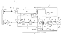
- FIG. 1A shows an exemplary embodiment of a test set-up 10 .
- the test set-up 10 comprises a signal processor 11 , which has a generator 12 .
- the test set-up 10 comprises a digital-analog converter 13 and an excitation coil 14 .
- An output of the generator 12 is connected to an input of the digital-analog converter 13 .
- An output of the digital-analog converter 13 is coupled to the excitation coil 14 .
- the test set-up 10 comprises an excitation amplifier 15 that is arranged between the output of the digital-analog converter 13 and the excitation coil 14 .
- a device being tested 16 is arranged near the excitation coil 14 .
- the test set-up 10 has a receiving coil 17 and an AD converter 21 .
- the receiving coil 17 is implemented as an absolute coil.
- the test set-up 10 implements an absolute channel test method.
- the receiving coil 17 is located close to the device being tested 16 .
- An output of the receiving coil 17 is coupled to an input of an AD converter 21 .
- the test set-up 10 comprises a receiving amplifier 20 , which couples the receiving coil 17 to the AD converter 21 .
- An amplification factor of the receiving amplifier 20 can be set by the signal processor 11 .
- the filter arrangement 22 comprises an input filter 29 .
- the test set-up 10 has a demodulator 27 .
- the demodulator 27 is implemented as a digital demodulator.
- the input filter 29 is arranged between the band-pass filter 25 and the other decimation unit 26 and the demodulator 27 .
- a signal input of the demodulator 27 is coupled to an output of the input filter 29 .
- the filter arrangement 22 comprises a subtractor 31 , which connects the input filter 29 to the demodulator 27 .
- the demodulator 27 comprises first and second multipliers 32 , 33 , which are connected to the signal input and two demodulator inputs 28 , 28 ′ of the demodulator 27 . Furthermore, the demodulator 27 comprises a demodulator filter 34 and a demodulator decimation unit 35 , which are downstream to the first and second multipliers 32 , 33 . Moreover, the test set-up 10 comprises a display 38 , which is coupled to the demodulator 27 on the input side. The test set-up 10 comprises a clock generator 39 . The clock generator 39 is coupled to a clock input of the signal processor 11 , a clock input of the digital-analog converter 13 , as well as a clock input of the AD converter 21 .
- the test set-up 10 comprises an analog-digital converter arrangement 18 , abbreviated AD-converter arrangement.
- the AD-converter arrangement 18 comprises the AD converter 21 as well as a portion of the filter arrangement 22 ,
- the AD-converter arrangement 18 has the low-pass filter 23 , the decimation unit 24 , the band-pass filter 25 , and the other decimation unit 26 .
- the signal processer 11 comprises another part of the filter arrangement 22 and the demodulator 27 .
- the signal processor 11 has the input filter 29 and the subtractor 31 .
- the clock generator 32 provides a clock signal CLK with a clock frequency CLK.
- the clock signal CLK is sent to the AD-converter arrangement 18 , the digital-analog converter 13 , and the signal processor 11 .
- the clock signal CLK thus synchronizes the processes in the signal processor 11 , the digital-analog converter 13 , as well as the AD-converter arrangement 18 .
- the generator 12 provides a generator signal SEG in the form of digital values.
- the digital-analog converter 13 generates a digital-analog-converter signal SDA from the generator signal SEG.
- the digital-analog-converter signal SDA is amplified by means of the excitation amplifier 15 and sent as an excitation signal SE to the excitation coil 14 .
- a coil signal SP can be picked up on the receiving coil 17 .
- the coil signal SP is amplified by the receiving amplifier 20 and sent to the AD converter 22 as an amplified coil signal SP′.
- the AD converter arrangement 18 generates an input signal SDE from the coil signal SP or the amplified coil signal SP′.
- the input signal is a digital signal.
- the AD converter 21 converts the amplified coil signal SP′ into a converter output signal SW.
- the AD converter 21 scans the amplified coil signal SP′ at a converter scan frequency f a .
- the converter scan frequency f a is equal to the clock frequency f CLK of the clock generator 31 .
- the coil signal SP is scanned at constant intervals.
- the time interval between two scan times is 1/f a and is constant.
- the converter scan frequency f a is independent of the value of the excitation frequency f m and also remains constant during a change of the excitation frequency f m .
- the filter arrangement 22 generates a demodulator input signal SD from the converter output signal SW.
- the converter output signal SW is filtered by means of the low-pass filter 23 and converted with respect to the scan frequencies by means of the decimation unit 24 .
- the decimation unit 24 implements conversion of a high scan frequency to a low scan frequency, i.e., down-sampling.
- the thus generated signal is filtered by means of the band-pass filter 25 and converted again with respect to the scan frequency by means of the additional decimation unit 26 .
- the input signal SDE that is provided by the AD converter arrangement 18 thus has a scan frequency f a′ .
- the scan rate f a′ of the input signal SDE is less than the converter scan rate f a .
- f a R 1 *f a′
- R 1 is a first reduction factor.
- the first reduction factor R 1 is an integer or a rational number. In this case, R 1 >0.
- the signal processor 11 controls the filter arrangement 22 , in particular, the decimation unit 24 and the band-pass filter 25 , via control lines.
- the input signal SDE reflects values that are generated at identical time intervals.
- the time interval between two values of the input signal SDE is 1/f n′ .
- the time interval is constant.
- the subtractor 31 provides, on the output side, a demodulator input signal SD, which is a function of a difference between the short-term signal low-pass filter SK and the long-term signal low-pass filter SE
- the demodulator input signal SD is fed to the demodulator 27 .
- the signal processor 11 provides two demodulator signals DS, DS′ in the form of sine values or cosine values to the first and second multipliers 32 , 33 via the demodulator inputs 28 , 28 ′.
- the provision of the sine and cosine values by the signal processor 11 is done with the scan frequency f a′ of the input signal SDE.
- the sine value and the cosine value, which are sent to the first and second multipliers 32 , 33 form a sine oscillation or a cosine oscillation with the excitation frequency f m .
- the plot of the sine values of the demodulator signal DS, which are sent to the first multiplier 32 thus corresponds to the phase response of the generator signal SEG provided by the generator 12 .
- the demodulation frequency of the demodulator signal DS, DS′ is thus the excitation frequency f m .
- the first multiplier 32 multiplies the demodulator signal DS in the form of sine values with the demodulator input signal SD.
- the second multiplier 33 multiplies the othe demodulator signal DS′ in the form of cosine values with the demodulator input signal SD.
- the first demodulator output signal S 1 provided by the first multiplier 32 and the second demodulator output signal S 2 provided by the second multiplier 33 are filtered by means of the demodulator filter 34 and the demodulator decimation unit 35 and reduced relative to the scan frequency and issued as first and second wanted signals SN 1 , SN 2 to first and second wanted signal outputs 36 , 37 of the demodulator 27 .
- the first wanted signal SN 1 reflects the imaginary portion
- the second wanted signal SN 2 reflects the real portion of the wanted signal.
- the first and second wanted signals SN 1 , SN 2 are depicted as points on the display 38 .
- an X coordinate of the point corresponds to the first wanted signal SN 1
- a Y coordinate of the point corresponds to the second wanted signal SN 2 .
- the signal processor 11 implements the input filter 29 , the subtractor 31 , as well as the demodulator 27 by means of a software-implemented method.
- the signal processor 11 performs the method for processing the input signal SDE on-line.
- the low-pass filter 23 , the band-pass filter 25 , and the demodulator filter 34 are designed as finite impulse response filters, abbreviated FIR filters.
- the input filter 29 is implemented as an infinite impulse response filter, abbreviated IIR filter.
- the low-pass filter 23 and the decimation unit 24 are integrated in a unit.
- a frequency divider is arranged between the clock generator 39 and the AD converter 21 , which divides the clock frequency f CLK with a whole factor L 1 .
- f CLK f a *L 1 .
- the filter arrangement 22 is divided into the AD converter arrangement 18 and the signal processor 11 in a different way.
- the test set-up 10 comprises an anti-aliasing filter, which is arranged between the receiving coil 17 and the input of the AD converter 22 .
- the anti-aliasing filter is implemented as a receiving low-pas filter.
- the filter can be referred to as an anti-scan-interference filter.
- FIG. 1B shows an exemplary embodiment of the input filter 29 , as it can be implemented in the test set-up 10 according to FIG. 1A .
- the input filter 29 comprises the first number M of low-pass filter arrangements 40 , 41 , 42 .
- a first low-pass filter arrangement 40 comprises a first short-term low-pass filter 43 and a first long-term low-pass filter 44 .
- a second low-pass filter arrangement 41 correspondingly comprises a second short-term low-pass filter and a second long-term low-pass filter 45 , 46 .
- the input filter 29 comprises additional short-term and long-term low-pass filters.
- an Mth low-pass filter arrangement 42 comprises an Mth short-term low-pass filter 47 and an Mth long-term low-pass filter 48 .
- the input filter 29 comprises an input switch 49 as well as an output switch 50 and another output switch 51 .
- the input switch 49 couples the filter input 30 of the input filter 29 alternately to the input of the first, the second, up to the Mth low-pass filter arrangement 40 , 41 , 42 .
- the input of the first low-pass filter arrangement 40 is connected to the input of the first short-term low-pass filter 43 and the input of the first long-term low-pass filter 44 .
- the signal processor 11 controls the input switch 49 with a control signal SC in such a way that the first value of the first number M of values of the input signal SDE of the first low-pass filter arrangement 40 is sent to the second value of the second low-pass filter arrangement 41 as well as the Mth value of the Mth low-pass filter arrangement 42 .
- the same is repeated with the next M values of the input signal SDE, i.e., in the following periods of the excitation signal SE.
- the short-term low-pass filters 43 , 45 , 47 filter the respective value of the input signal with a short time constant compared to a time constant of the long-term low-pass filters 44 , 46 , 48 .
- the short-term low-pass filters 43 , 45 , 47 forward a first number Z 1 of the periods of the excitation signal SE.
- the long-term low-pass filters 44 , 46 , 48 forward a second number Z 2 of periods of the excitation signal SE. In this case, the following holds true: Z 1 ⁇ Z 2 .
- the output switch 50 alternately switches an output of the first short-term low-pass filter 43 , an output of the second short-term low-pass filter 45 , and an output of the Mth short-term low-pass filter 47 to the first input of the subtractor 31 .
- the additional output switch 51 alternately switches an output of the first long-term low-pass filter 44 , an output of the second long-term low-pass filter 46 , and an output of the Mth long-term low-pass filter 48 to the second input of the subtractor 31 .
- the difference between the short-term signal low-pass filter SK and the long-term signal low-pass filter SL of the first low-pass filter arrangement 40 thus is present as the demodulator input signal SD, and then the difference between the two output signals of the second low-pass filter arrangement 41 up to the difference between the two output signals of the Mth low-pass filter arrangement 42 are available.
- the input filter 29 is implemented as an FIR filter.
- the input filter 29 can optionally also be designed for scan rate reduction.
- the short- and long-term low-pass filters 43 to 48 can produce a scan rate reduction.
- FIG. 1C shows a graphic depiction of the harmonic demodulation, as it is implemented by means of the input filter 29 .
- the input signal SDE that is provided by the AD converter arrangement 18 is shown in magnitude and phase here.
- the second and third values of the first number M of values are sent to the second short-term and/or long-term low-pass filters 45 , 46 of the second low-pass filter arrangement 41 or to the Mth short-term low-pass filter 47 and the Mth long-term low-pass filter 48 of the Mth low-pass filter arrangement 42 .
- a short-term signal low-pass filter SK in the example at the output of the first short-term low-pass filter 43 can be calculated such that:
- SK SK ′ + SDE - SK ′ 2 M , whereby SK is the current value of the short-term signal low-pass filter, SK′ is the previous value of the short-term signal low-pass filter, SDE is the current value of the input signal, and M is the first number.
- FIG. 1C depicts additional values for the rational ratio between the scan frequency f a′ and the excitation frequency f m .
- a conventional digital demodulation can be performed using the following equations:
- the first signal S 1 which reproduces the alternating components, can be calculated with the following equations:
- the scan frequency fa′ also called sample frequency, for demodulation frequency, which is identical to the excitation frequency fm, is in a harmonic ratio
- the first number M of angles is produced during the second number N of periods of the excitation signal SE.
- fa′*N fm*M:
- Z 1 is a first number of periods and Z 2 is a second number of periods of the excitation signal SE, over which averaging is done.
- ⁇ n is the alternating component.
- the second signal S 2 is calculated by using the cosine function instead of the sine function.
- the AD converter arrangement 18 performs the analog-digital conversion, for example, with 24-bit resolution.
- the low-pass filter arrangements 40 , 41 , 42 in the input filter 29 have, for example, an accuracy of 32 or 40 bits.
- the subtractor 31 is designed to scale the demodulator input signal SD to, for example, 16 bits. To process the alternating component ⁇ n in the demodulator 27 , a computational accuracy of, for example, 16 bits, is adequate.
- the demodulator 27 calculates the real and imaginary portions of the first and second signals S 1 , S 2 , and it implements post-filtering of the real and imaginary portions for generating the wanted signals SN 1 , SN 2 .
- the scan frequency fa′ can advantageously be matched to the excitation frequency fm.
- the excitation frequency fm can be converted between preset values during operation.
- the rational ratio M/N is set as a function of the value of the excitation frequency fm.
- the rational ratio M/N is reduced with an increasing value of the excitation frequency fm.
- the rational ratio M/N is set in such a way that the scan frequency fa′ is smaller han a maximum scan rate that can be processed by the signal processor 11 .
- the rational ratio M/N is set in such a way that the interval between the scan frequency fa′ and the maximum scan frequency that can be processed by the signal processor 11 is as small as possible.
- a table 62 in the signal processor 11 which contains the first number M of sine values and cosine values, is adequate for the storage of the demodulator signals DS, DS′ at an excitation frequency fm. Also, for several preset values of the excitation frequency fm, the storage requirement for the table 62 in the signal processor 11 is low.
- the test set-up 10 implements a harmonic demodulation.
- the harmonic demodulation with sliding mean value formation makes it possible for a signal processor 11 that is designed for low processing speeds to be adequate for the signal processing. In the signal processor 11 , only multiplications with sine/cosine table values and simple computation operations are performed.
- the filter arrangement 22 comprises a signal processing system 29 ′.
- the signal processing system 29 ′ is arranged at the position of the input filter 29 that is depicted in FIG. 1A .
- the signal processing system 29 ′ couples the band-pass filter 25 to the demodulator 27 .
- the signal processing system 29 ′ has a conversion system 29 ′′.
- the conversion system 29 ′′ is designed to provide only one value as the demodulator input signal SD to the scan frequency reduction of a first number P of values of the input signal SDE.
- the first number P is an integer and is greater than or equal to 1. In one embodiment, the first number P is greater than 1 .
- the signal processing system 29 ′ performs this at high and mean values of the excitation frequency fm.
- the signal processing system 29 ′ is adjustable. If the excitation frequency fm has a low value, the signal processing system 29 ′ activates a signal low-pass filter 29 ′′.
- the signal processor 11 thus performs different method steps for signal processing of the input signal SDE depending on the value of the excitation frequency fm. While at high and mean values of the excitation frequency fm of P values, only one value of the input signal SDE is passed on, at low values of the excitation frequency fm, the input signal SDE is low-pass-filtered with an FIR characteristic 29 ′′′.
- the signal processing system thus comprises the conversion system 29 ′′ for high and mean excitation frequencies fm and the signal low-pass filter 29 ′′′ for low excitation frequencies fm.
- the filter arrangement 22 has an additional low-pass filter 52 , which is downstream of the low-pass filter 23 . Furthermore, the filter arrangement 22 has an output low-pass filter 53 as well as a switch device 54 .
- the switch device 54 switches either the band-pass filter 25 or the output low-pass filter 53 between the additional low-pass filter 52 and the signal processing system 29 ′.
- the band-pass filter 25 ensures signal band limitation before demodulation.
- the signal processing system 29 ′ has an accuracy of 32 bits.
- the demodulator 27 is designed for a 32-bit accuracy.
- the word length in the demodulator 27 is 32 bits.
- the sine table that is used in the demodulator 27 is 16 bits long.
- the first filter ladder 55 has a band-rejection filter 57 .
- the band-rejection filter 57 is downstream to the first multiplier 33 .
- a high-pass filter 58 , a low-pass filter 59 , another high-pass filter 60 as well as another low-pass filter 61 are downstream to the band-rejection filter 57 .
- the band-rejection filter 57 and the low-pass filter 59 are implemented as FIR (Finite Impulse Response) filters.
- the high-pass filters 58 , 60 as well as the additional low-pass filter 61 are implemented as IIR (Infinite Impulse Response) filters.
- the first wanted signal SN 1 indicates the imaginary portion
- the second wanted signal SN 2 indicates the real portion of the wanted signal.
- the signal processor 11 performs the complex sine/cosine demodulation and the additional signal processing.
- the digital input signal SDE is real-valued and requires only a signal path.
- the analog circuit expense is reduced to one-half compared to a real-valued and imaginary-valued digital input signal.
- a savings in cost and a very compact structure are made possible.
- digital antecedents in comparison to analog circuits have a higher accuracy and are subject to smaller fluctuations.
- converter scan rate f a 5000 kHz
- pass-band frequencies of 980 kHz to 1020 kHz stop-band frequencies of 750 kHz to 1250 kHz
- pass-band fluctuation 0.1 (-dB) stop-band fluctuation 120 (-dB)
- filter length 96 32-bit floating point calculation
- FIR equiripple
- the signal processor 11 generates the excitation frequency fm and the demodulation frequency of the demodulation signals DS, DS′ from the clock signal CLK.
- the excitation frequency f m , the demodulation frequency of the demodulation signals DS, DS′ and the scan frequency f a of the AD converter 21 are synchronous to one another and are set exactly.
- the demodulation frequency is the frequency with which the sine and cosine values are provided to the demodulator 27 .
- the clock signal CLK, the excitation signal SE, as well as a trigger signal of the AD converter 21 which has the converter scan rate f a , are synchronous to one another.
- the excitation signal SE has a phase offset. With the phase offset, the running time in the filter arrangement 22 is compensated, so that no phase rotation is present between the demodulator input signal SD and the demodulator signal DS, DS′.
- n is the phase increment.
- the length of the sine table does not have any effect on the frequency accuracy, which by itself is fixed by the accumulator word width N 1 and is f CLK /2 N1 . If n is a whole multiple of 2 N1-M1 , the output table values correspond exactly to the scan times of the desired sine function.
- a quantization noise with the standard deviations s for rounded table values and a signal-to-noise ratio SNR are produced according to the following equation:
- the error signal in this case has a discrete line spectrum.
- SFDR 6 ⁇ M 1 ⁇ 4 [dB]
- a 16k table with 2 14 entries with 14-bit word length is adequate.
- the amplitude-quantization noise is then ⁇ 86 dB and with the presence of phase noise, the maximum spectral line of the error signal is at most ⁇ 80 dB relative to the sine amplitude.
- a rigid analog excitation low-pass filter 70 is required as a reconstruction low-pass filter; a rigid clock frequency f CLK is used.
- the 20 MHz clock of the AD converter 21 is also used as a clock signal CLK with the clock frequency f CLK .
- the phase accumulator in the generator 12 has a word width of 32 bits. While no phase error occurs in the upper frequency range of the excitation frequency fm of 1 MHz to 16 kHz, at the low frequencies, it is reduced below 4 kHz of the entire signal-to-noise ratio to approximately 67 dB as a result of the phase noise. In the demodulation, because of the narrow band limitation, higher-frequency interference is all the more strongly suppressed the lower the excitation frequency fm is.
- the demodulation also produces a frequency component in the double demodulation frequency fm′ in addition to the even component, and said demodulation frequency fm′ is suppressed by the degree 3 linear-phase FIR band-rejection filter 57 , 57 ′ with only four coefficients.
- An accuracy of 16 bits for the coefficients is advantageously adequate.
- the band-rejection filter 57 , 57 ′ is located before the high-pass filter 58 , 58 ′, since otherwise, because of the high amplitude of the basic frequency harmonic, only very slow attenuated step responses would be the result.
- the high-pass filter 58 , 58 ′ is advantageously implemented as an IIR filter, since its limiting frequency and thus the transient response time can be switched very simply.
- the degree 1 IIR-high-pass filter 58 , 58 ′ makes possible an error voltage suppression with quick adjustment.
- the IIR filter type allows for a coefficient switch-over with the shortest transient response behavior, since a minimum phase system is present. Based on the degree 1, the computing expense is low.
- R′ total reduction factor
- the signal processor 11 Since usually the device being tested 16 is moved past the receiver coil 17 , the signal processor 11 has to analyze the data of the input signal SDE online to make possible a localization of the error in the device being tested 16 .
- the excitation frequency f m 1 MHz
- the FIR low-pass filter 59 , 59 ′ with 23 coefficients and a band limitation to 15 kHz follows as a post-filter. In this connection, the scan frequency is reduced to 208 kHz.
- the low-pass filter 59 , 59 ′ is used in addition to correct the damping of the degree 3 band-rejection filter 57 , 57 ′ in the pass-band range.
- a very high damping of the frequency component in the double demodulation frequency is generated by the zero point of the FIR band-rejection filter 57 , 57 ′ and the post-filtering in the following reduction low-pass filter 59 , 59 ′.
- FIR filters can be used very efficiently for scan rate reduction. Because of the finite impulse response, the calculation at the scan frequency f a′ or the reduced scan frequency fa′′ is possible. FIR filters have a linear phase, so that distortions are avoided, and the time signal shape is maintained.
- the wanted signal band can lie closer to the excitation frequency fm, specifically, for example, up to a factor of 3 below the excitation frequency fm (and thus no longer has to be at least less than 1/10 of the excitation frequency fm).
- the narrow-band filtering produces high noise immunity and a reduction of noise.
- an IIR high-pass filter 60 , 60 ′ and a degree 2 or 4 IIR-low-pass filter 61 , 61 ′ follows the reduction low-pass filter 59 .
- the IIR high-pass filter 60 , 60 ′ and the IIR low-pass filter 61 , 61 ′ are recursive filters and are rigidly set.
- the IIR high-pass filter 60 , 60 ′ and the IIR low-pass filter 61 , 61 ′ are automatically readjusted as a function of the test speed.
- optionally coefficients with 32 -bit word lengths may be necessary.
- the IIR high-pass filter 60 , 60 ′ and the IIR low-pass filter 61 , 61 ′ are automatically matched by the test set-up 10 to the test speed, with which the device being tested 16 is examined.
- the coefficients of the filters 60 , 60 ′, 61 , 61 ′ are calculated and switched by the signal processor 11 .
- the IIR high-pass filter 60 , 60 ′ and the IIR low-pass filter 61 , 61 ′ produce a filtering of the low-frequency wanted signal for noise suppression.
- the IIR high-pass filter 58 , 58 ′ is used primarily in a differential coil arrangement, as shown in FIG. 3A . If only one coil, namely the receiving coil 17 , is used on the receiving side, the test set-up 10 implements an absolute channel. In the case of an absolute channel, the bias-IIR-high-pass filter 58 , 58 ′ is replaced by a subtractor, which subtracts a compensation value from the signal. The compensation value for the zero adjustment is determined and readjusted by the signal processor 11 .
- the low-pass filter 23 has a scan rate reduction by a factor of 4, and the band-pass filter 25 and the output low-pass filter 53 in each case have a scan rate reduction by a factor of 2.
- a scan rate reduction factor of the other low-pass filter 52 can be set.
- the clock frequency fCLK is typically 20 MHz and is used both by the AD converter arrangement 18 and by the generator 12 .
- a 10 MHz clock is used as a scan rate for reducing the load of the signal processor 11 for the digital generation of the excitation signal SE with the excitation frequency fm instead of 20 MHz.
- the phase increment is increased.
- the maximum amplitude deviation is then ⁇ 0.14 dB.
- the excitation filter 70 which is used as a reconstruction filter, can then have a degree of 5 to 6 with an edge steepness of 30 to 36 dB per octave.
- the signal processor 11 calculates the sine and cosine values of the demodulator signal DS, DS′.
- the calculation can be done by series approximation or by means of the CORDIC (COrdinate Rotation DIgital Computer) method.
- FIG. 3A shows an exemplary embodiment of a detail of the test set-up 10 as it can be used, for example, in the test setup according to FIG. 1A .
- the additional receiving coil 72 of the test set-up 10 is arranged in series in the receiving coil 17 .
- the receiving coil 17 and the additional receiving coil 72 thus form a differential coil arrangement.
- FIG. 3B shows an exemplary embodiment of another detail of the test set-up 10 according to FIG. 2 .
- the test setup 10 has the band-pass 25 and the demodulator 27 , between which the signal processing system 29 ′ is provided.
- the signal processing system 29 ′ is explained for high values of the excitation frequency fm, in which the conversion system 29 ′′ is activated.
- the conversion system 29 ′′ is used for scan rate reduction.
- the conversion system 29 ′′ is implemented as a switch 80 .
- An input of the switch 80 is connected to the band-pass filter 25 .
- the switch 80 has the first number P of outputs.
- the first output of the switch 80 is connected to the demodulator 27 .
- the conversion system 29 ′′ reduces the scan frequency f a′ by the whole factor of P to the reduced scan frequency f a′′ .
- the conversion system 29 ′′ can therefore also be referred to as a downward mixer.
- the conversion system 29 ′′ is implemented as a decimator. It can also be referred to as a resampler.
- the conversion system 29 ′′ is thus implemented in that only each Pth value is transmitted. The intermediate values are omitted.
- the signal processor 11 implements the conversion system 29 ′′ and the demodulator 27 by storage and further processing by means of demodulation of each Pth value of the input signal SDE.
- the signal processor 11 receives the unnecessary P ⁇ 1 value of the input signal SDE but does not demodulate the latter.
- the signal processing system 29 ′ implements a conversion method using the conversion system 29 ′′.
- the conversion method does not require any explicit multiplication by changing the scan frequency f a′ to the reduced scan frequency fa′′.
- the operations in the signal processing system 29 ′ and the subsequent operations are implemented by the signal processor 11 with the reduced scan frequency f a′′ .
- a signal processor 11 can be used at low speed.
- the AD conversion, filtering and scan rate reduction and subsequent demodulation are carried out with observance of the sampling theorem and the folding properties of time-discrete systems and with use of aliasing.
- a rational ratio between the scanning frequency f a′ , and the mean frequency fm is not necessary.
- the method can also be implemented without a rational ratio between the scan frequency f a′ , f a′′ and the excitation frequency f m .
- FIGS. 4A to 4D show an exemplary embodiment of the spectra in the test set-up 10 according to FIG. 3B .
- the excitation frequency fm has the value of 1015 kHz.
- FIG. 4A the frequency spectrum of the coil signal SP is indicated.
- FIG. 4B shows the input signal SDE after scanning with the converter scan rate fa and the band-pass filtering by means of the band-pass filter 25 .
- FIG. 4C shows the rate-reduced demodulator input signal SD that is provided by the conversion system 29 ′′ of the signal processing system 29 ′.
- the scan frequency fa′ in this case is scan-rate-reduced to the reduced scan frequency f a′′ , and the excitation frequency f m is converted to a demodulation frequency after conversion f m′ .
- the demodulation frequency after conversion fm′ can also be referred to as an intermediate frequency.
- the first and second wanted signals SN 1 , SN 2 are indicated, which are generated by demodulation, low-pass filtering, and additional scan rate reduction within the demodulator 27 .
- the coil signal SP is narrow-banded and amplitude- and phase-modulated.
- the coil signal has a bandwidth of 15 kHz in this example.
- the band-pass filter 25 has a band-pass range of +/ ⁇ 15 kHz and a band-rejection limit of +/ ⁇ 170 kHz to the band limitation.
- the coil signal SP is thus converted, i.e., mixed downward to the intermediate frequency fm′ according to the following equation:
- the modulo demodulation method With the method of frequency conversion by downward mixing, the filtered signal of the band-pass filter 25 is converted to a lower intermediate frequency. This is suitable primarily for high excitation frequencies fm. For low excitation frequencies fm, however, the signal of the band-pass filter 25 is directly demodulated after low-pass filtering by means of the signal low-pass filter 29 ′′′.
- the demodulation can be carried out in the original position or in the reverse position of the frequency.
- k ⁇ f a′′ ⁇ f m′ ⁇ ( k+ 0.5) ⁇ f a′′ where K is an integer. This corresponds to the requirement f m′ ⁇ f a′′ /2 .
- no reverse position of the frequency takes place.
- the condition has to be met: f b ⁇ f m′ ⁇ f a′′ /2 ⁇ f B
- the band-pass signal at fm′ is then complex-demodulated with sin(2 ⁇ fm′ t) and cos(2 ⁇ fm′ t).
- the intermediate frequency fm′, the reduced scan frequency f a′′ , and thus the scan frequency f a′ are in a harmonic ratio to one another.
- the reduced scan rate fa′′ is a rational multiple of the intermediate frequency m′.
- f m′ /f a′′ a/b holds true, whereby a and b are integers.
- the largest possible data rate for a 16-bit word length is approximately 50 M word/s.
- R>2 in each case only the scan values in a ratio R/2 are further used. All other read-in values are ignored.
- the demodulation frequency f m′ is unlike the excitation frequency f m . However, at lower frequencies without downward mixing, the demodulation frequency is equal to the excitation frequency f m .
- the method can thus have the following advantages: A complete digital demodulation and filtering is carried out. In addition, a band-pass filtering is carried out in the AD-converter arrangement 18 . The operations are performed on the intermediate frequency at a lower scan frequency. Thus, there is a savings in computing time. The use of a processor at low speed is made possible. Only an AD converter 21 and a signal path are required between the receiver coil 17 up to the demodulator 27 for demodulation of real and imaginary portions, i.e., in-phase/quadrature components, on the intermediate frequency. By contrast, in general two AD converters are required in the case of conventional underscanning with direct demodulation and conversion into the base band.
- the test set-up 10 performs the test method online. The test set-up 10 can be implemented economically.
Abstract
Description
whereby SK is the current value of the short-term signal low-pass filter, SK′ is the previous value of the short-term signal low-pass filter, SDE is the current value of the input signal, and M is the first number.
f a′ =M/N·f m
whereby the table word width b is in bits. In all other values of n, the cutting of the non-integer table indices [ai*2−(N1-M1)] results in a phase error, which produces an additional noise component in the output in the form of an amplitude error that is modulated with the excitation frequency fm. For small phase errors ep, the following are produced for the digital-analog-converter signal SDA of the digital-analog converter 13:
SFDR=6·M1−4 [dB]
k·f a″ <f m′<(k+0.5)·f a″
where K is an integer. This corresponds to the requirement fm′<fa″/2 . Thus, no reverse position of the frequency takes place. In addition, the condition has to be met:
f b <f m′ <f a″/2−f B
Claims (11)
Priority Applications (1)
| Application Number | Priority Date | Filing Date | Title |
|---|---|---|---|
| US13/548,921 US8841902B2 (en) | 2012-01-20 | 2012-07-13 | Testing device and testing method for non destructive detection of a defect in a test piece by means of an eddy current |
Applications Claiming Priority (2)
| Application Number | Priority Date | Filing Date | Title |
|---|---|---|---|
| US201261588730P | 2012-01-20 | 2012-01-20 | |
| US13/548,921 US8841902B2 (en) | 2012-01-20 | 2012-07-13 | Testing device and testing method for non destructive detection of a defect in a test piece by means of an eddy current |
Publications (2)
| Publication Number | Publication Date |
|---|---|
| US20130187643A1 US20130187643A1 (en) | 2013-07-25 |
| US8841902B2 true US8841902B2 (en) | 2014-09-23 |
Family
ID=48796708
Family Applications (1)
| Application Number | Title | Priority Date | Filing Date |
|---|---|---|---|
| US13/548,921 Active 2032-11-24 US8841902B2 (en) | 2012-01-20 | 2012-07-13 | Testing device and testing method for non destructive detection of a defect in a test piece by means of an eddy current |
Country Status (1)
| Country | Link |
|---|---|
| US (1) | US8841902B2 (en) |
Cited By (1)
| Publication number | Priority date | Publication date | Assignee | Title |
|---|---|---|---|---|
| US11169298B2 (en) | 2016-07-20 | 2021-11-09 | Halliburton Energy Services, Inc. | Shaped sensor coil for attenuating motion-induced noise during remote field testing of pipe |
Families Citing this family (9)
| Publication number | Priority date | Publication date | Assignee | Title |
|---|---|---|---|---|
| US9350985B2 (en) * | 2013-09-25 | 2016-05-24 | Olympus Ndt, Inc. | Method and circuitry for removing circling drifts in NDT/NDI measurement display |
| CN108027254B (en) | 2015-08-11 | 2021-04-06 | 大陆-特韦斯股份有限公司 | Device for measuring a measurement variable |
| DE102015215331A1 (en) * | 2015-08-11 | 2017-02-16 | Continental Teves Ag & Co. Ohg | Electronic control unit |
| DE102016202403A1 (en) | 2016-02-17 | 2017-08-17 | Continental Teves Ag & Co. Ohg | sensor |
| DE102016202402A1 (en) | 2016-02-17 | 2017-08-17 | Continental Teves Ag & Co. Ohg | sensor |
| US11231392B2 (en) | 2016-12-27 | 2022-01-25 | Industrial Technology Research Institute | Detecting device and method thereof |
| TWI674415B (en) * | 2016-12-27 | 2019-10-11 | 財團法人工業技術研究院 | Detecting device and method thereof |
| US11130692B2 (en) * | 2017-06-28 | 2021-09-28 | Uop Llc | Process and apparatus for dosing nutrients to a bioreactor |
| CN116953065B (en) * | 2023-09-20 | 2024-01-23 | 中国核电工程有限公司 | Positioning method for weld defects of stainless steel cladding |
Citations (10)
| Publication number | Priority date | Publication date | Assignee | Title |
|---|---|---|---|---|
| JPH05292133A (en) | 1992-04-14 | 1993-11-05 | Japan Radio Co Ltd | Digital demodulation circuit |
| US5811682A (en) * | 1995-12-13 | 1998-09-22 | Ebara Corporation | Electromagnetic acoustic transducer EMAT and inspection system with EMAR |
| US20040066189A1 (en) | 2002-10-08 | 2004-04-08 | Estell Lopez | Dynamic gain control in a digital eddy current signal processor |
| WO2006007826A1 (en) | 2004-07-19 | 2006-01-26 | Prüftechnik Dieter Busch AG | Method and device for the non-destructive and contactless detection of flaws in a test piece moved relative to a probe |
| DE102004051506A1 (en) | 2004-10-21 | 2006-04-27 | Prüftechnik Dieter Busch AG | Method for detecting faults in a test piece moved relative to a probe in a non-destructive and non-contact manner using a filter whose frequency is set depending on the fault frequency |
| EP1995590A1 (en) | 2007-05-23 | 2008-11-26 | GE Inspection Technologies, LP | Method and apparatus for digital measurement of an eddy current signal |
| GB2457496A (en) | 2008-02-15 | 2009-08-19 | Ge London Patent Operation | A system for detecting defects using eddy currents |
| US7757557B2 (en) * | 2005-10-14 | 2010-07-20 | Olympus Ndt | Ultrasonic detection measurement system using a tunable digital filter with 4x interpolator |
| JP2010271317A (en) | 2009-05-20 | 2010-12-02 | Prueftechnik Dieter Busch Ag | Instrument and method for measuring induction |
| DE102012100460A1 (en) | 2012-01-20 | 2013-07-25 | Prüftechnik Dieter Busch AG | Test arrangement and test method for nondestructive detection of an error in a test specimen by means of an eddy current |
-
2012
- 2012-07-13 US US13/548,921 patent/US8841902B2/en active Active
Patent Citations (15)
| Publication number | Priority date | Publication date | Assignee | Title |
|---|---|---|---|---|
| JPH05292133A (en) | 1992-04-14 | 1993-11-05 | Japan Radio Co Ltd | Digital demodulation circuit |
| US5811682A (en) * | 1995-12-13 | 1998-09-22 | Ebara Corporation | Electromagnetic acoustic transducer EMAT and inspection system with EMAR |
| US20040066189A1 (en) | 2002-10-08 | 2004-04-08 | Estell Lopez | Dynamic gain control in a digital eddy current signal processor |
| US7423424B2 (en) | 2004-07-19 | 2008-09-09 | Prüftechnik Dieter Busch AG | Method and apparatus for the non-destructive and contactless detection of faults in a test piece which is moved relative to a probe |
| US20070080681A1 (en) | 2004-07-19 | 2007-04-12 | Prueftecnik Dieter Busch Ag | Method and device for the non-destructive and contactless detection of flaws in a test piece moved relative to a probe |
| WO2006007826A1 (en) | 2004-07-19 | 2006-01-26 | Prüftechnik Dieter Busch AG | Method and device for the non-destructive and contactless detection of flaws in a test piece moved relative to a probe |
| US7443156B2 (en) | 2004-07-19 | 2008-10-28 | Pruftechnik Dieter Busch Ag | Apparatus and method for identifying defects on objects or for locating objects |
| EP1794582B1 (en) | 2004-07-19 | 2009-05-27 | Prüftechnik Dieter Busch Ag | Method and device for the non-destructive and contactless detection of flaws in a test piece moved relative to a probe |
| DE102004051506A1 (en) | 2004-10-21 | 2006-04-27 | Prüftechnik Dieter Busch AG | Method for detecting faults in a test piece moved relative to a probe in a non-destructive and non-contact manner using a filter whose frequency is set depending on the fault frequency |
| US7757557B2 (en) * | 2005-10-14 | 2010-07-20 | Olympus Ndt | Ultrasonic detection measurement system using a tunable digital filter with 4x interpolator |
| EP1995590A1 (en) | 2007-05-23 | 2008-11-26 | GE Inspection Technologies, LP | Method and apparatus for digital measurement of an eddy current signal |
| US20080290866A1 (en) | 2007-05-23 | 2008-11-27 | Cuffe John M | Method and apparatus for digital measurement of an eddy current signal |
| GB2457496A (en) | 2008-02-15 | 2009-08-19 | Ge London Patent Operation | A system for detecting defects using eddy currents |
| JP2010271317A (en) | 2009-05-20 | 2010-12-02 | Prueftechnik Dieter Busch Ag | Instrument and method for measuring induction |
| DE102012100460A1 (en) | 2012-01-20 | 2013-07-25 | Prüftechnik Dieter Busch AG | Test arrangement and test method for nondestructive detection of an error in a test specimen by means of an eddy current |
Cited By (1)
| Publication number | Priority date | Publication date | Assignee | Title |
|---|---|---|---|---|
| US11169298B2 (en) | 2016-07-20 | 2021-11-09 | Halliburton Energy Services, Inc. | Shaped sensor coil for attenuating motion-induced noise during remote field testing of pipe |
Also Published As
| Publication number | Publication date |
|---|---|
| US20130187643A1 (en) | 2013-07-25 |
Similar Documents
| Publication | Publication Date | Title |
|---|---|---|
| US8841902B2 (en) | Testing device and testing method for non destructive detection of a defect in a test piece by means of an eddy current | |
| EP2618140B1 (en) | Test set-up and test method for non-destructive detection of a flaw in a device under test by means of an eddy current | |
| JP5389311B2 (en) | Signal processing device | |
| EP2725726B1 (en) | Method and apparatus for magnitude and phase response calibration of receivers | |
| CN105676008B (en) | Digital electric field sensor | |
| CN104122444A (en) | All-digital intermediate frequency spectrum analyzer and spectrum analyzing method | |
| US20040066189A1 (en) | Dynamic gain control in a digital eddy current signal processor | |
| CN110971231A (en) | Digital lock-in amplifier incorporating ratiometric operation | |
| JP2015087271A (en) | Property measurement device with surface acoustic wave sensor | |
| CN110263482B (en) | Eddy impedance solving method and device based on cross correlation algorithm | |
| US20170307567A1 (en) | Electrical signal processing device | |
| Shoupeng et al. | Quadrature demodulation based circuit implementation of pulse stream for ultrasonic signal FRI sparse sampling | |
| JP4350488B2 (en) | Voltage, current, active power, reactive power, frequency measuring device and measuring method in power system | |
| CN109541309B (en) | Spectrum analyzer and signal processing method thereof | |
| JP2007003458A (en) | Digital orthogonal lock-in detecting method and device | |
| JP2006017486A (en) | Spectral analysis method using nuclear magnetic resonance and nuclear magnetic resonance system | |
| JP5797843B2 (en) | Method and apparatus for testing material under test in a non-destructive manner | |
| US6873149B1 (en) | Method and system for eddy current proximity system noise reduction | |
| WO2023199085A1 (en) | Filtering device and method to extract signal from noise | |
| Zhengming et al. | A new-developed multi-frequency impedance analyzing instrument used for eddy current testing based on DSP | |
| JP2017166905A (en) | Phase detection circuit and surface acoustic wave sensor | |
| JP6995403B2 (en) | Asynchronous FRA and synchronous detector | |
| KR101606467B1 (en) | Device for inspecting defects of test body using eddy current | |
| Rosado et al. | Real-time processing of multi-frequency eddy currents testing signals | |
| US10511317B2 (en) | Electric quantity measuring device comprising an analog-digital converter |
Legal Events
| Date | Code | Title | Description |
|---|---|---|---|
| AS | Assignment |
Owner name: PRUEFTECHNIK DIETER BUSCH AG, GERMANY Free format text: ASSIGNMENT OF ASSIGNORS INTEREST;ASSIGNORS:LYSEN, HEINRICH;BRAEU, WERNER;REEL/FRAME:028547/0193 Effective date: 20120705 |
|
| STCF | Information on status: patent grant |
Free format text: PATENTED CASE |
|
| MAFP | Maintenance fee payment |
Free format text: PAYMENT OF MAINTENANCE FEE, 4TH YR, SMALL ENTITY (ORIGINAL EVENT CODE: M2551) Year of fee payment: 4 |
|
| FEPP | Fee payment procedure |
Free format text: ENTITY STATUS SET TO UNDISCOUNTED (ORIGINAL EVENT CODE: BIG.) |
|
| AS | Assignment |
Owner name: PRUEFTECHNIK DIETER BUSCH GMBH, GERMANY Free format text: CHANGE OF NAME;ASSIGNOR:PRUEFTECHNIK DIETER BUSCH AG;REEL/FRAME:054547/0408 Effective date: 20200917 |
|
| MAFP | Maintenance fee payment |
Free format text: PAYMENT OF MAINTENANCE FEE, 8TH YEAR, LARGE ENTITY (ORIGINAL EVENT CODE: M1552); ENTITY STATUS OF PATENT OWNER: LARGE ENTITY Year of fee payment: 8 |