JP5388712B2 - Foreign matter removal device - Google Patents
Foreign matter removal device Download PDFInfo
- Publication number
- JP5388712B2 JP5388712B2 JP2009142706A JP2009142706A JP5388712B2 JP 5388712 B2 JP5388712 B2 JP 5388712B2 JP 2009142706 A JP2009142706 A JP 2009142706A JP 2009142706 A JP2009142706 A JP 2009142706A JP 5388712 B2 JP5388712 B2 JP 5388712B2
- Authority
- JP
- Japan
- Prior art keywords
- drive signal
- transformer
- generation circuit
- switching element
- signal generation
- Prior art date
- Legal status (The legal status is an assumption and is not a legal conclusion. Google has not performed a legal analysis and makes no representation as to the accuracy of the status listed.)
- Expired - Fee Related
Links
Images


Classifications
-
- B—PERFORMING OPERATIONS; TRANSPORTING
- B08—CLEANING
- B08B—CLEANING IN GENERAL; PREVENTION OF FOULING IN GENERAL
- B08B7/00—Cleaning by methods not provided for in a single other subclass or a single group in this subclass
- B08B7/0035—Cleaning by methods not provided for in a single other subclass or a single group in this subclass by radiant energy, e.g. UV, laser, light beam or the like
Description
本発明は、ビデオカメラ、デジタルスチルカメラ等の撮像装置の光学部品に付着した異物を除去する技術に関する。 The present invention relates to a technique for removing foreign substances adhering to optical components of an imaging apparatus such as a video camera or a digital still camera.
近年、撮像装置においては、光学センサの分解能の向上と共に、使用中に光学系に付着するゴミ(異物)が撮影画像に影響を及ぼすことが問題となってきている。特に、ビデオカメラ、スチルカメラに搭載される撮像素子の分解能はめざましく向上している。そのため、撮像素子の近くに配置されている赤外線カットフィルタ、光学ローパスフィルタ等に、外部からの埃や内部の機械的な摺擦面で生ずる摩耗粉等の異物が付着すると、次のような現象が起こる。すなわち、撮像素子の分解能が高く、さらに撮像素子面での像のぼけが少ないため、撮影画像に異物が写り込むことがある。 2. Description of the Related Art In recent years, in an imaging apparatus, there has been a problem that dust (foreign matter) adhering to an optical system during use has an effect on a captured image as the resolution of an optical sensor is improved. In particular, the resolution of image sensors mounted on video cameras and still cameras has been remarkably improved. Therefore, when foreign matter such as dust from the outside or wear powder generated on the internal mechanical friction surface adheres to the infrared cut filter, optical low-pass filter, etc., located near the image sensor, the following phenomenon occurs: Happens. That is, since the resolution of the image sensor is high and the image blur on the image sensor surface is small, foreign matter may appear in the captured image.
撮像装置において塵埃が付着した場合、使用者が塵埃を拭き取ることで画像品位は回復するが、機器の使用中に付着した塵埃は撮影後に確認するほかない。その間に撮影した画像については塵埃の画像が映り込むため、ソフトウェアによる画像の修正が必要となる。 When dust adheres to the image pickup apparatus, the image quality is restored by wiping the dust off by the user, but the dust attached during use of the device can only be checked after shooting. Since the dust image appears in the images taken during that time, it is necessary to correct the images by software.
そこで、振動を利用した防塵機構を備えたカメラが商品化されている。ここで、この振動を利用した防塵機構は、多大な振動エネルギーを必要とする。そのため、特許文献1には次のような技術が開示されている。少なくとも1つの振動モードの振動の節と他の振動モードの振動の節との節間隔が他の節間隔より小さい節間に、支持部材を配置し、電気機械エネルギ変換素子によって光学部品に同時に複数の振動モードを生じさせる。これにより、振動エネルギの損失を抑え、塵埃除去装置の消費エネルギを低減させながら光学部品に付着した塵埃を除去すると共に、発熱による光学特性の劣化を抑制する。 Therefore, cameras equipped with a dust-proof mechanism using vibration have been commercialized. Here, the dust-proof mechanism using this vibration requires a large amount of vibration energy. Therefore, Patent Document 1 discloses the following technique. A support member is disposed between nodes having a vibration node of at least one vibration mode and a vibration node of another vibration mode smaller than the other node intervals, and a plurality of optical members are simultaneously formed by an electromechanical energy conversion element. The vibration mode is generated. Thereby, loss of vibration energy is suppressed, dust attached to the optical component is removed while reducing energy consumption of the dust removing device, and deterioration of optical characteristics due to heat generation is suppressed.
特許文献1に開示されているような複数の振動モードを同時に発生させるための方法を、図7に示すようなデジタルスチルカメラに装備された塵埃除去装置の構成図を参照して説明する。 A method for simultaneously generating a plurality of vibration modes as disclosed in Patent Document 1 will be described with reference to a configuration diagram of a dust removing device equipped in a digital still camera as shown in FIG.
図7において、デジタルスチルカメラは、撮像素子部14−1及びカバーガラス14−2を有する撮像素子パッケージ14と、塵埃除去装置とを備えている。塵埃除去装置は、振動体を構成する圧電素子2−1,2−2と、支持部材61と、駆動回路13と、光学フィルタ51とを備えて構成される。
In FIG. 7, the digital still camera includes an image
しかしながら、従来の塵埃除去機構においては、複数の振動モードを発生させるために、複数の電気機械エネルギー変換素子である圧電素子を、複数の駆動周波数で駆動する必要がある。そのため、出力周波数の異なる駆動回路を複数必要とする。また、光学フィルタ51に圧電素子を配置する場合、撮像領域外に配置する必要があり、複数の圧電素子を配置した場合、高価な光学フィルタの必要面積が増大する問題があった。また、光学フィルタの大きさが増大すると、カメラの小型化の障害となる場合もあった。
However, in the conventional dust removal mechanism, in order to generate a plurality of vibration modes, it is necessary to drive the piezoelectric elements that are a plurality of electromechanical energy conversion elements at a plurality of driving frequencies. For this reason, a plurality of drive circuits having different output frequencies are required. Further, when a piezoelectric element is arranged on the
本発明は上述した課題に鑑みてなされたものであり、その目的は、光学部品に付着した異物を除去する場合の消費エネルギーを低減させるとともに、電気機械エネルギー変換素子を削減して高価な光学フィルタの面積を削減することである。 The present invention has been made in view of the above-described problems, and an object of the present invention is to reduce energy consumption when removing foreign matters adhering to an optical component, and reduce an electromechanical energy conversion element and an expensive optical filter. It is to reduce the area.
上述した課題を解決し、目的を達成するために、本発明に係わる異物除去装置は、光学部品に付着した異物を除去する異物除去装置であって、前記光学部品の一端に配置された圧電素子と、電源と、前記圧電素子を駆動するための電圧を生成するトランスであって、1次側巻線と、2次側巻線とを有し、前記2次側巻線が前記圧電素子に接続されているトランスと、第1の周波数の第1の駆動信号を発生する第1の駆動信号発生回路と、ソースが前記電源に、ドレインが前記トランスの1次側巻線の一端に、ゲートが前記第1の駆動信号発生回路に接続される第1のポジティブ側スイッチング素子と、ソースがグランドに、ドレインが前記トランスの1次側巻線の一端に、ゲートが前記第1の駆動信号発生回路に接続される第1のネガティブ側スイッチング素子と、前記第1の周波数とは異なる第2の周波数の第2の駆動信号を発生する第2の駆動信号発生回路と、ソースが前記電源に、ドレインが前記トランスの1次側巻線の他端に、ゲートが前記第2の駆動信号発生回路に接続される第2のポジティブ側スイッチング素子と、ソースがグランドに、ドレインが前記トランスの1次側巻線の他端に、ゲートが前記第2の駆動信号発生回路に接続される第2のネガティブ側スイッチング素子と、を備えることを特徴とする。 To solve the above problems and achieve the object, the foreign matter removing apparatus according to the present invention, there is provided a foreign matter removing device for removing foreign matter adhered to an optical component, a piezoelectric element that is disposed on one end of the optical components When a power supply, wherein a transformer for generating a voltage for driving the piezoelectric element, a primary winding, and a secondary winding, the secondary winding is the piezoelectric element A connected transformer, a first drive signal generating circuit for generating a first drive signal of a first frequency, a source at the power source, a drain at one end of the primary winding of the transformer, and a gate Includes a first positive-side switching element connected to the first drive signal generation circuit, a source to ground, a drain to one end of the primary winding of the transformer, and a gate to the first drive signal generation First negative connected to the circuit A switching element, the first and second drive signal generating circuit for generating a second driving signal different from the second frequency is the frequency, the source is the power source, the primary winding of the drain is the transformer A second positive-side switching element having a gate connected to the second drive signal generation circuit, a source connected to the ground, a drain connected to the other end of the primary winding of the transformer, and a gate connected to the other end of the transformer and wherein the obtaining Bei and a second negative side switching element connected to the second drive signal generating circuit.
本発明によれば、光学部品に付着した異物を除去する場合の消費エネルギーを低減させるとともに、電気機械エネルギー変換素子を削減して高価な光学フィルタの面積を削減することが可能となる。 ADVANTAGE OF THE INVENTION According to this invention, while reducing the energy consumption when removing the foreign material adhering to an optical component, it becomes possible to reduce an electromechanical energy conversion element and to reduce the area of an expensive optical filter.
以下、本発明の好適な実施形態について、図面を参照して詳細に説明する。 DESCRIPTION OF EMBODIMENTS Hereinafter, preferred embodiments of the present invention will be described in detail with reference to the drawings.
(第1の実施形態)
図1は、本発明の第1の実施形態に係わる撮像装置としてのデジタルスチルカメラに装備された塵埃除去装置(異物除去装置)を示す図であり、図1(a)は、塵埃除去装置の構成を示す分解斜視図である。図1(b)は、撮像素子パッケージ及び光学フィルタに対するシール部材の接合構造を示す断面図である。
(First embodiment)
FIG. 1 is a diagram showing a dust removing device (foreign matter removing device) equipped in a digital still camera as an imaging device according to the first embodiment of the present invention. FIG. 1 (a) is a diagram of the dust removing device. It is a disassembled perspective view which shows a structure. FIG. 1B is a cross-sectional view showing a joint structure of the seal member to the image sensor package and the optical filter.
図1において、デジタルスチルカメラは、撮像素子部14−1及びカバーガラス14−2を有する撮像素子パッケージ14と、塵埃除去装置(異物除去装置)とを備えている。塵埃除去装置は、圧電素子2と、支持部材11,12と、駆動回路13と、光学フィルタ51(光学部品)とを備えて構成される。
In FIG. 1, the digital still camera includes an image
本実施形態では、撮像素子部14−1の前面に配置される光学フィルタ51を塵埃除去装置の振動部材として用いる。光学フィルタ51の長手方向一端部には、圧電素子2が接着されている。圧電素子2には、駆動回路13により交番電圧(駆動信号)が印加される。撮像素子パッケージ14は、撮像素子部14−1をカバーガラス14−2で封止した構造となっている。
In the present embodiment, the
支持部材11,12は、撮像素子パッケージ14と光学フィルタ51との間に粘着材料により固定されている。支持部材11,12は、撮像素子パッケージ14と光学フィルタ51の相対的な位置決めをすると共に、光学フィルタ51を支持している。シール部材21は、支持部材11,12の上端部同士を結ぶように接続されている。シール部材22は、支持部材11,12の下端部同士を結ぶように接続されている。シール部材21,22は、支持部材11,12と共に閉じた枠形状を構成している。
The
シール部材21の縦断面形状を図1(b)に拡大して示す。尚、シール部材22の断面形状も同様であり、図示は省略する。シール部材21,22の光学フィルタ51に対する接触面の幅は、シール部材21,22の撮像素子パッケージ14に対する接触面の幅と比較して小さく形成されている。シール部材21,22は、縦断面形状がリップ形状となっている。
The longitudinal cross-sectional shape of the sealing
上記のように、支持部材11,12を撮像素子パッケージ14及び光学フィルタ51に粘着材料により固定している。そのため、支持部材11,12及びシール部材21,22により、撮像素子パッケージ14と光学フィルタ51との間に密閉空間を構成することができる。これにより、外部の塵埃(異物)が撮像素子パッケージ14と光学フィルタ51の間に侵入するのを防止することができる。
As described above, the
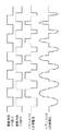
図2は、塵埃除去装置により発生させる振動モードの振動形状を示す図である。図2は、圧電素子2により光学フィルタ51に生じさせる振動モードの振動形状と支持部材11,12の位置関係を示している。本実施形態では、曲げ4次の振動モードを第1の振動モード、曲げ5次の振動モードを第2の振動モードとしている。即ち、第1の振動モード及び第2の振動モードは、光学フィルタ51を厚さ方向へ曲げ変形させる面外振動モードである。第1の振動モード及び第2の振動モードの振動は、光学フィルタ51に同時或いは順次加えられる。
FIG. 2 is a diagram illustrating a vibration shape of a vibration mode generated by the dust removing device. FIG. 2 shows a positional relationship between the vibration shape of the vibration mode generated in the
第1の振動モードの振動41の5箇所の節31A〜31Eと、第2の振動モードの振動42の6箇所の節32A〜32Fの間隔は、中央付近の節31Cと節32Cとの間隔及び節31Cと節32Dとの間隔が最も広い。両端の節31Aと節32Aとの間隔及び節31Eと節32Fとの間隔が最も接近している。
The distance between the five
本実施形態では、第1及び第2の振動モードの節の間隔が小さい、両端の節31Aと節32Aとの間及び節31Eと節32Fとの間に、それぞれ支持部材11,12を位置させている。支持部材11,12は、光学フィルタ51と撮像素子パッケージ14との間のギャップを管理するのに十分な剛性を有し、振動を阻害しない柔軟性を有する弾性部材からなる。支持部材11,12を上記の位置に配置することにより、光学フィルタ51に加える振動が阻害されることを抑制している。
In the present embodiment, the
上記の支持部材11及び12により光学フィルタ51の支持を行っているため、シール部材21,22は封止の機能だけを有すればよい。そのため、シール部材21,22を、柔軟性を持たせ且つ光学フィルタ51に対する接触面積を狭く構成することができる。従って、シール部材21,22が第1及び第2の振動モードの振動の複数の腹位置にわたって配置されても、光学フィルタ51に加える振動を阻害しにくい。これにより、光学フィルタ51に付着した塵埃を振動により効果的に除去することができる。
Since the
図3は本実施形態に係る塵埃除去装置を駆動するための電気回路の回路構成を示す図である。図3において、電源101は圧電素子2を駆動するための電源であり、カメラの場合にはカメラ全体を駆動するための電源と共用する。第1の駆動信号発生回路102は圧電素子2に発生させる複数の振動モードのうち、第1の振動モードを生成するための第1の周波数の信号を発生させる。第2の駆動信号発生回路103は圧電素子2に発生させる複数の振動モードのうち、第2の振動モードを生成するための第2の周波数の信号を発生させる。第1及び第2の駆動信号発生回路102,103は、それぞれ、必要な振動モードのうち一つの振動モードに対応する周波数信号を発生する。また、これらの周波数信号は、それぞれ異なる振動を発生させるために異なる周波数を持つ。
FIG. 3 is a diagram showing a circuit configuration of an electric circuit for driving the dust removing device according to the present embodiment. In FIG. 3, a power source 101 is a power source for driving the
第1の駆動回路104は第1の駆動信号発生回路102で発生された駆動信号で制御され、101を電源として、トランス110の1次側巻き線111の一端を駆動する。また、第2の駆動回路105は第2の駆動信号発生回路103で発生された駆動信号で制御され、101を電源として、トランス110の1次側巻き線111の他端を駆動する。P−chMOSFET106,108は第1及び第2の駆動回路104,105を構成する第1のポジティブ側スイッチング素子および第2のポジティブ側スイッチング素子である。
The
P−chMOSFET106は、ソースが電源101に、ドレインがトランス110の1次側巻線111の一端、ゲートが第1の駆動信号発生回路102の出力に接続されている。P−chMOSFET108は、ソースが電源101に、ドレインがトランス110の1次側巻線111の他端に、ゲートが第2の駆動信号発生回路103の出力に接続されている。
The P-
N−chMOSFET107,109は駆動回路104,105を構成する第1のネガティブ側スイッチング素子および第2のネガティブ側スイッチング素子である。N−chMOSFET107は、ソースがグランドに、ドレインがトランス110の1次側巻線111の一端に、ゲートが第1の駆動信号発生回路102の出力に接続されている。N−chMOSFET109は、ソースがグランドに、ドレインがトランス110の1次側巻線111の他端に、ゲートが第2の駆動信号発生回路103の出力に接続されている。P−chMOSFET106とN−chMOSFET107のの組み合わせで、第1の駆動回路104を構成する。P−chMOSFET108とN−chMOSFET109の組み合わせで、第2の駆動回路105を構成する。
N-
トランス110の2次側巻線112は、圧電素子2に接続されており、トランス110の1次側巻線111の電流変化に従って磁気結合により電圧を発生し、圧電素子2に駆動電圧を印加する。
A secondary winding 112 of the
図4は本実施形態に係る塵埃除去装置を駆動するための電気回路の信号の状態を示す図である。具体的には、第1の駆動回路104の出力、第2の駆動回路105の出力、トランス110の1次側巻線111に流れる電流、トランス110の2次側巻線112に発生する電圧を示している。ここで、2次側巻線112に発生する電圧は、圧電素子2の容量成分とトランス110の2次側巻線112のインダクタンス成分により正弦波の電圧が生成される。また、トランス110の2次側巻線112に発生する電圧は、トランス110の1次側巻線111と2次側巻線112の巻線比により、圧電素子2を駆動するのに適正な電圧に昇圧される。
FIG. 4 is a diagram illustrating a signal state of an electric circuit for driving the dust removing device according to the present embodiment. Specifically, the output of the
さらに、トランス110の2次側巻線112に発生した電圧は、第1の駆動回路104と第2の駆動回路105の出力周波数を合成した波形となる。つまり、第1の駆動信号発生回路102の出力と第2の駆動信号発生回路103から出力された周波数の信号の二つの周波数信号の成分を含む合成信号となっている。
Further, the voltage generated in the secondary winding 112 of the
この信号で、圧電素子2を駆動することで、圧電素子2に第1及び第2の振動モードの複数の振動を発生させることができる。
By driving the
以上、説明したように、第1の実施形態によれば、一つの圧電素子2に同時に複数の節を発生させることができるため、必要な圧電素子の数量を削減できるとともに、高価な光学フィルタの面積を削減し、低コスト化と小型化を図ることができる。
As described above, according to the first embodiment, since a plurality of nodes can be simultaneously generated in one
(第2の実施形態)
上記の第1の実施形態では、トランスの1次側巻線の一端と他端を異なる周波数の駆動回路の出力で駆動することで二つの周波数の信号を合成した。これに対し、これから説明する第2の実施形態では、トランスの1次側巻き線を2つに分けて配置している。
(Second Embodiment)
In the first embodiment described above, signals at two frequencies are synthesized by driving one end and the other end of the primary winding of the transformer with outputs of drive circuits having different frequencies. On the other hand, in the second embodiment to be described, the primary winding of the transformer is divided into two parts.
本実施形態におけるデジタルスチルカメラに装備された塵埃除去装置の外観構成は、第1の実施形態で説明した図1、図2と同様であるためここでは説明を省略する。 Since the external configuration of the dust removing device installed in the digital still camera in the present embodiment is the same as that in FIGS. 1 and 2 described in the first embodiment, the description thereof is omitted here.
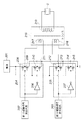
図5は、本実施形態に係わる塵埃除去装置を駆動するための電気回路の回路構成を示す図である。図5において、電源201は圧電素子2を駆動するための電源であり、カメラの場合にはカメラ全体を駆動するための電源と共用する。第1の駆動信号発生回路202は圧電素子2に発生させる複数の振動モードのうち、第1の振動モードを生成するための第1の周波数の信号を発生させる。第2の駆動信号発生回路203は圧電素子2に発生させる複数の振動モードのうち、第2の振動モードを生成するための第2の周波数の信号を発生させる。そして、第1及び第2の駆動信号発生回路202,203は、それぞれ、必要な振動モードのうち一つの振動モードに対応する周波数信号を発生する。また、これらの周波数信号は、それぞれ異なる振動を発生させるために異なる周波数を持つ。
FIG. 5 is a diagram showing a circuit configuration of an electric circuit for driving the dust removing apparatus according to the present embodiment. In FIG. 5, a
第1の駆動回路204は第1の駆動信号発生回路202で発生された駆動信号で制御され、201を電源として、トランス216の第1の1次側巻き線217を駆動する。第2の駆動回路205は第2の駆動信号発生回路203で発生された駆動信号で制御され、201を電源として、トランス216の第2の1次側巻き線218を駆動する。インバータ206,207(第1のインバータおよび第2のインバータ)は、第1及び第2の駆動信号発生回路202,203からの信号を反転させる。P−chMOSFET208,210,212,214は駆動回路204,205を構成する第1ないし第4のポジティブ側スイッチング素子である。
The
P−chMOSFET208(第1のポジティブ側スイッチング素子)は、ソースが電源201に、ドレインがトランス216の第1の1次側巻線217の一方に、ゲートが第1の駆動信号発生回路202の出力に接続されている。P−chMOSFET210(第2のポジティブ側スイッチング素子)は、ソースが電源201に、ドレインがトランス216の第1の1次側巻線217他方に、ゲートがインバータ206に接続されている。P−chMOSFET212(第3のポジティブ側スイッチング素子)は、ソースが電源201に、ドレインがトランス216の第2の1次側巻線218の一方に、ゲートが第2の駆動信号発生回路203の出力に接続されている。P−chMOSFET214(第4のポジティブ側スイッチング素子)は、ソースが電源201に、ドレインがトランス216の第2の1次側巻線218の他方に、ゲートがインバータ207に接続されている。
In the P-ch MOSFET 208 (first positive side switching element), the source is the
N−chMOSFET209,211,213,215は第1及び第2の駆動回路204,205を構成する第1ないし第4のネガティブ側スイッチング素子である。N−chMOSFET209(第1のネガティブ側スイッチング素子)は、ソースがグランドに、ドレインがトランス216の第1の1次側巻線217の一方に、ゲートが第1の駆動信号発生回路202の出力に接続されている。N−chMOSFET211(第2のネガティブ側スイッチング素子)は、ソースがグランドに、ドレインがトランス216の第1の1次側巻線217の他方に、ゲートがインバータ206に接続されている。N−chMOSFET213(第3のネガティブ側スイッチング素子)は、ソースがグランドに、ドレインがトランス216の第2の1次側巻線218の一方に、ゲートが第2の駆動信号発生回路203の出力に接続されている。N−chMOSFET215(第4のネガティブ側スイッチング素子)は、ソースがグランドに、ドレインがトランス216の第2の1次側巻線218の他方に、ゲートがインバータ207に接続されている。
N-
そして、P−chMOSFET208,210とN−chMOSFET209,211の組み合わせで、駆動回路204を構成する。P−chMOSFET212,214とN−chMOSFET213,215の組み合わせで、駆動回路205を構成する。
The
トランス216の2次側巻線219は、圧電素子2に接続されており、トランス216の第1の1次側巻線217及び第2の1次側巻線218の電流変化に従って磁気結合により電圧を発生し、圧電素子2に駆動電圧を印加する。
The secondary side winding 219 of the
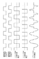
図6は本実施形態に係わる塵埃除去装置を駆動するための電気回路の信号の状態を示す図である。具体的には、第1の駆動信号発生回路202の出力、第2の駆動信号発生回路203の出力、トランス216の第1の1次側巻線217に流れる電流、トランス216の第2の1次側巻線218に流れる電流、トランス216の2次側巻線219に発生する電圧を示している。ここで、2次側巻線219に発生する電圧は、圧電素子2の容量成分とトランス216の2次側巻線219のインダクタンス成分により正弦波の電圧が生成される。また、トランス216の2次側巻線219に発生する電圧は、トランス216の1次側巻線217,218と2次側巻線219の巻線比により、圧電素子2を駆動するのに適正な電圧に昇圧される。
FIG. 6 is a diagram showing a signal state of an electric circuit for driving the dust removing apparatus according to the present embodiment. Specifically, the output of the first drive
さらに、トランス216の2次側巻線219に発生した電圧は、第1の駆動信号発生回路202と第2の駆動信号発生回路203の出力周波数を合成した波形、つまり、二つの周波数信号の成分を含む合成信号となっている。この信号で、圧電素子2を駆動することで、圧電素子2に第1及び第2の振動モードの複数の振動を発生させることができる。
Further, the voltage generated in the secondary winding 219 of the
以上、説明したように、本実施形態によれば、一つの圧電素子2に同時に複数の節を発生させることができるため、必要な圧電素子の数量を削減できるとともに、高価な光学フィルタの面積を削減し、低コスト化と小型化を図ることができる。
As described above, according to the present embodiment, since a plurality of nodes can be simultaneously generated in one
なお、上記の第1及び第2の実施形態では、デジタルスチルカメラに塵埃除去装置を適用した場合を例に挙げて説明したが、本発明はこれに限定されるものではない。塵埃除去装置は、デジタルスチルカメラ以外にも、複写機、ファクシミリ、スキャナ、ビデオカメラ等の各種機器に適用することができる。 In the first and second embodiments, the case where the dust removing device is applied to the digital still camera has been described as an example. However, the present invention is not limited to this. The dust removing device can be applied to various devices such as a copying machine, a facsimile, a scanner, and a video camera in addition to a digital still camera.
Claims (6)
前記光学部品の一端に配置された圧電素子と、
電源と、
前記圧電素子を駆動するための電圧を生成するトランスであって、1次側巻線と、2次側巻線とを有し、前記2次側巻線が前記圧電素子に接続されているトランスと、
第1の周波数の第1の駆動信号を発生する第1の駆動信号発生回路と、
ソースが前記電源に、ドレインが前記トランスの1次側巻線の一端に、ゲートが前記第1の駆動信号発生回路に接続される第1のポジティブ側スイッチング素子と、
ソースがグランドに、ドレインが前記トランスの1次側巻線の一端に、ゲートが前記第1の駆動信号発生回路に接続される第1のネガティブ側スイッチング素子と、
前記第1の周波数とは異なる第2の周波数の第2の駆動信号を発生する第2の駆動信号発生回路と、
ソースが前記電源に、ドレインが前記トランスの1次側巻線の他端に、ゲートが前記第2の駆動信号発生回路に接続される第2のポジティブ側スイッチング素子と、
ソースがグランドに、ドレインが前記トランスの1次側巻線の他端に、ゲートが前記第2の駆動信号発生回路に接続される第2のネガティブ側スイッチング素子と、を備えることを特徴とする異物除去装置。 A foreign matter removing device for removing foreign matter attached to an optical component,
A piezoelectric element disposed on one end of the optical component,
Power supply,
A transformer for generating a voltage for driving the piezoelectric element, the transformer having a primary side winding and a secondary side winding, wherein the secondary side winding is connected to the piezoelectric element When,
A first drive signal generating circuit for generating a first drive signal having a first frequency;
A first positive switching element having a source connected to the power source, a drain connected to one end of the primary winding of the transformer, and a gate connected to the first drive signal generation circuit;
A first negative-side switching element having a source connected to ground, a drain connected to one end of the primary winding of the transformer, and a gate connected to the first drive signal generation circuit;
A second drive signal generating circuit for generating a second drive signal having a second frequency different from the first frequency;
A second positive-side switching element having a source connected to the power source, a drain connected to the other end of the primary winding of the transformer, and a gate connected to the second drive signal generation circuit;
Source connected to the ground, and characterized on the other end of the drain is the transformer primary winding, a second negative side switching element having a gate connected to said second drive signal generating circuit, that obtain Bei the Foreign matter removal device to do.
前記光学部品の一端に配置された圧電素子と、
電源と、
前記圧電素子を駆動するための電圧を生成するトランスであって、第1および第2の1次側巻線と、2次側巻線とを有し、前記2次側巻線が前記圧電素子に接続されているトランスと、
第1の周波数の第1の駆動信号を発生する第1の駆動信号発生回路と、
ソースが前記電源に、ドレインが前記トランスの前記第1の1次側巻線の一端に、ゲートが前記第1の駆動信号発生回路に接続される第1のポジティブ側スイッチング素子と、
ソースがグランドに、ドレインが前記トランスの前記第1の1次側巻線の前記一端に、ゲートが前記第1の駆動信号発生回路に接続される第1のネガティブ側スイッチング素子と、
前記第1の駆動信号発生回路の出力を反転する第1のインバータと、
ソースが前記電源に、ドレインが前記トランスの前記第1の1次側巻線の他端に、ゲートが前記第1のインバータに接続される第2のポジティブ側スイッチング素子と、
ソースがグランドに、ドレインが前記トランスの前記第1の1次側巻線の前記他端に、ゲートが前記第1のインバータに接続される第2のネガティブ側スイッチング素子と、
前記第1の周波数とは異なる第2の周波数の第2の駆動信号を発生する第2の駆動信号発生回路と、
ソースが前記電源に、ドレインが前記トランスの前記第2の1次側巻線の一端に、ゲートが前記第2の駆動信号発生回路に接続される第3のポジティブ側スイッチング素子と、
ソースがグランドに、ドレインが前記トランスの前記第2の1次側巻線の前記一端に、ゲートが前記第2の駆動信号発生回路に接続される第3のネガティブ側スイッチング素子と、
前記第2の駆動信号発生回路の出力を反転する第2のインバータと、
ソースが前記電源に、ドレインが前記トランスの前記第2の1次側巻線の他端に、ゲートが前記第2のインバータに接続される第4のポジティブ側スイッチング素子と、
ソースがグランドに、ドレインが前記トランスの前記第2の1次側巻線の前記他端に、ゲートが前記第2のインバータに接続される第4のネガティブ側スイッチング素子と、を備えることを特徴とする異物除去装置。 A foreign matter removing device for removing foreign matter attached to an optical component,
A piezoelectric element disposed on one end of the optical component,
Power supply,
A transformer for generating a voltage for driving the piezoelectric element, the transformer including first and second primary windings and a secondary winding, wherein the secondary winding is the piezoelectric element. A transformer connected to the
A first drive signal generating circuit for generating a first drive signal having a first frequency;
A first positive switching element having a source connected to the power source, a drain connected to one end of the first primary winding of the transformer, and a gate connected to the first drive signal generating circuit;
A first negative switching element having a source connected to ground, a drain connected to the one end of the first primary winding of the transformer, and a gate connected to the first drive signal generation circuit;
A first inverter for inverting the output of the first drive signal generation circuit;
A second positive switching element having a source connected to the power source, a drain connected to the other end of the first primary winding of the transformer, and a gate connected to the first inverter;
A second negative switching element having a source connected to ground, a drain connected to the other end of the first primary winding of the transformer, and a gate connected to the first inverter;
A second drive signal generating circuit for generating a second drive signal having a second frequency different from the first frequency;
A third positive switching element having a source connected to the power source, a drain connected to one end of the second primary winding of the transformer, and a gate connected to the second drive signal generation circuit;
A third negative-side switching element having a source connected to ground, a drain connected to the one end of the second primary winding of the transformer, and a gate connected to the second drive signal generation circuit;
A second inverter for inverting the output of the second drive signal generation circuit;
A fourth positive switching element having a source connected to the power source, a drain connected to the other end of the second primary winding of the transformer, and a gate connected to the second inverter;
Source connected to the ground, the other end of the drain of said transformer second primary winding, and a fourth negative-side switching element having a gate connected to said second inverter, that obtain Bei the A foreign matter removing device.
Priority Applications (2)
| Application Number | Priority Date | Filing Date | Title |
|---|---|---|---|
| JP2009142706A JP5388712B2 (en) | 2009-06-15 | 2009-06-15 | Foreign matter removal device |
| US12/796,800 US8237328B2 (en) | 2009-06-15 | 2010-06-09 | Foreign substance removing apparatus |
Applications Claiming Priority (1)
| Application Number | Priority Date | Filing Date | Title |
|---|---|---|---|
| JP2009142706A JP5388712B2 (en) | 2009-06-15 | 2009-06-15 | Foreign matter removal device |
Publications (3)
| Publication Number | Publication Date |
|---|---|
| JP2010288238A JP2010288238A (en) | 2010-12-24 |
| JP2010288238A5 JP2010288238A5 (en) | 2012-07-26 |
| JP5388712B2 true JP5388712B2 (en) | 2014-01-15 |
Family
ID=43306218
Family Applications (1)
| Application Number | Title | Priority Date | Filing Date |
|---|---|---|---|
| JP2009142706A Expired - Fee Related JP5388712B2 (en) | 2009-06-15 | 2009-06-15 | Foreign matter removal device |
Country Status (2)
| Country | Link |
|---|---|
| US (1) | US8237328B2 (en) |
| JP (1) | JP5388712B2 (en) |
Families Citing this family (2)
| Publication number | Priority date | Publication date | Assignee | Title |
|---|---|---|---|---|
| JP5381366B2 (en) * | 2008-06-26 | 2014-01-08 | 株式会社ニコン | Imaging device |
| JP5501902B2 (en) | 2010-09-03 | 2014-05-28 | オリンパスイメージング株式会社 | Vibrating device and imaging device using the same |
Family Cites Families (5)
| Publication number | Priority date | Publication date | Assignee | Title |
|---|---|---|---|---|
| JPH06274016A (en) * | 1993-03-19 | 1994-09-30 | Canon Inc | Image forming device |
| JP2000151285A (en) * | 1998-11-11 | 2000-05-30 | Oki Electric Ind Co Ltd | Amplitude modulation circuit |
| JP2006259162A (en) * | 2005-03-16 | 2006-09-28 | Olympus Imaging Corp | Optical device with dust-proof function |
| JP2007047198A (en) * | 2005-08-05 | 2007-02-22 | Olympus Imaging Corp | Optical equipment |
| JP4724584B2 (en) * | 2006-03-29 | 2011-07-13 | キヤノン株式会社 | Dust removing device, image reading device, and imaging device |
-
2009
- 2009-06-15 JP JP2009142706A patent/JP5388712B2/en not_active Expired - Fee Related
-
2010
- 2010-06-09 US US12/796,800 patent/US8237328B2/en not_active Expired - Fee Related
Also Published As
| Publication number | Publication date |
|---|---|
| US20100315711A1 (en) | 2010-12-16 |
| JP2010288238A (en) | 2010-12-24 |
| US8237328B2 (en) | 2012-08-07 |
Similar Documents
| Publication | Publication Date | Title |
|---|---|---|
| JP4724584B2 (en) | Dust removing device, image reading device, and imaging device | |
| JP5455057B2 (en) | Driving method of vibrating body, vibrating device, driving device having the vibrating device, dust removing device, and optical apparatus | |
| JP4759635B2 (en) | Vibration device | |
| JP5089065B2 (en) | Dust removal device | |
| JP2007228246A (en) | Dust eliminating device and driving method | |
| JP5383429B2 (en) | Vibrating device, driving device having the vibrating device, dust removing device, and optical apparatus | |
| JP5882796B2 (en) | Driving method for vibrating body, vibrating device, driving device having the vibrating device, and optical apparatus | |
| JP4759636B2 (en) | Vibration device | |
| US20120274243A1 (en) | Driving circuit for vibration apparatus | |
| US8493506B2 (en) | Imaging device unit and imaging apparatus for removing dust from an optical device | |
| JP5344134B2 (en) | Imaging device and optical device | |
| JP5388712B2 (en) | Foreign matter removal device | |
| JP5783708B2 (en) | Dust removing device and imaging device | |
| JP2009296356A (en) | Optical component and optical apparatus | |
| JP4905170B2 (en) | Dust removal device and imaging device | |
| JP2008211629A (en) | Imaging apparatus and optical device | |
| JP5262135B2 (en) | Optical components and optical equipment | |
| US8299418B2 (en) | Imaging device unit and photographing apparatus comprising a piezoelectric element mounted on a plate | |
| JP2015027671A (en) | Vibration device, driving device with vibration device, dust removal device, and optical equipment | |
| JP4834409B2 (en) | Dust remover | |
| JP5611434B2 (en) | Vibrating device, driving device having the vibrating device, dust removing device, and optical apparatus | |
| JP5228507B2 (en) | Optical component, imaging device and optical apparatus | |
| JP5245870B2 (en) | Optical apparatus and photographing apparatus | |
| US20110102896A1 (en) | Foreign substance removing apparatus | |
| JP2005331829A (en) | Electrostatic shutter device, optical equipment, and optical equipment having the shutter device, and camera |
Legal Events
| Date | Code | Title | Description |
|---|---|---|---|
| A521 | Request for written amendment filed |
Free format text: JAPANESE INTERMEDIATE CODE: A523 Effective date: 20120608 |
|
| A621 | Written request for application examination |
Free format text: JAPANESE INTERMEDIATE CODE: A621 Effective date: 20120608 |
|
| A977 | Report on retrieval |
Free format text: JAPANESE INTERMEDIATE CODE: A971007 Effective date: 20130418 |
|
| A131 | Notification of reasons for refusal |
Free format text: JAPANESE INTERMEDIATE CODE: A131 Effective date: 20130507 |
|
| A521 | Request for written amendment filed |
Free format text: JAPANESE INTERMEDIATE CODE: A523 Effective date: 20130702 |
|
| TRDD | Decision of grant or rejection written | ||
| A01 | Written decision to grant a patent or to grant a registration (utility model) |
Free format text: JAPANESE INTERMEDIATE CODE: A01 Effective date: 20130909 |
|
| A61 | First payment of annual fees (during grant procedure) |
Free format text: JAPANESE INTERMEDIATE CODE: A61 Effective date: 20131008 |
|
| LAPS | Cancellation because of no payment of annual fees |