JP2010288238A5 - - Google Patents
Download PDFInfo
- Publication number
- JP2010288238A5 JP2010288238A5 JP2009142706A JP2009142706A JP2010288238A5 JP 2010288238 A5 JP2010288238 A5 JP 2010288238A5 JP 2009142706 A JP2009142706 A JP 2009142706A JP 2009142706 A JP2009142706 A JP 2009142706A JP 2010288238 A5 JP2010288238 A5 JP 2010288238A5
- Authority
- JP
- Japan
- Prior art keywords
- drive signal
- transformer
- primary winding
- circuit
- source
- Prior art date
- Legal status (The legal status is an assumption and is not a legal conclusion. Google has not performed a legal analysis and makes no representation as to the accuracy of the status listed.)
- Granted
Links
Images
Description
上述した課題を解決し、目的を達成するために、本発明に係わる異物除去装置は、光学部品に付着した異物を除去する異物除去装置であって、光学部品の一端に配置された圧電素子と、前記圧電素子を駆動するための電圧を生成するトランスであって、1次側巻線と、2次側巻線とを有し、該2次側巻線が前記圧電素子に接続されているトランスと、第1の周波数の第1の駆動信号を発生する第1の駆動信号発生回路と、前記トランスの前記1次側巻線の一端に接続され、前記第1の駆動信号発生回路により生成された前記第1の駆動信号を前記1次側巻線の一端に加える第1の駆動回路と、第2の周波数の第2の駆動信号を発生する第2の駆動信号発生回路と、前記トランスの前記1次側巻線の他端に接続され、前記第2の駆動信号発生回路により生成された前記第2の駆動信号を前記1次側巻線の他端に加える第2の駆動回路と、を備え、前記第1の駆動信号の第1の周波数と前記第2の駆動信号の第2の周波数は互いに異なることを特徴とする。 In order to solve the above-described problems and achieve the object, a foreign matter removing apparatus according to the present invention is a foreign matter removing apparatus that removes foreign matter adhering to an optical component, and includes a piezoelectric element disposed at one end of the optical component, A transformer for generating a voltage for driving the piezoelectric element, the transformer having a primary side winding and a secondary side winding, the secondary side winding being connected to the piezoelectric element a transformer, is connected to the first drive signal generation circuit for generating a first drive signal of a first frequency, to one end of the primary winding of the transformer, generated by the first drive signal generating circuit A first drive circuit for applying the first drive signal applied to one end of the primary winding, a second drive signal generation circuit for generating a second drive signal of a second frequency, and the transformer Connected to the other end of the primary winding of the second drive signal generating circuit. And a second driving circuit for adding the generated second drive signal to the other end of the primary winding by, wherein the first frequency of the first drive signal the second driving signal the second frequency and wherein the Rukoto different from each other.
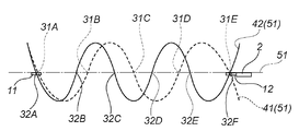
第1の振動モードの振動41の5箇所の節31A〜31Eと、第2の振動モードの振動42の6箇所の節32A〜32Fの間隔は、中央付近の節31Cと節32Cとの間隔及び節31Cと節32Dとの間隔が最も広い。両端の節31Aと節32Aとの間隔及び節31Eと節32Fとの間隔が最も接近している。
The distance between the five
Claims (8)
光学部品の一端に配置された圧電素子と、
前記圧電素子を駆動するための電圧を生成するトランスであって、1次側巻線と、2次側巻線とを有し、該2次側巻線が前記圧電素子に接続されているトランスと、
第1の周波数の第1の駆動信号を発生する第1の駆動信号発生回路と、
前記トランスの前記1次側巻線の一端に接続され、前記第1の駆動信号発生回路により生成された前記第1の駆動信号を前記1次側巻線の一端に加える第1の駆動回路と、
第2の周波数の第2の駆動信号を発生する第2の駆動信号発生回路と、
前記トランスの前記1次側巻線の他端に接続され、前記第2の駆動信号発生回路により生成された前記第2の駆動信号を前記1次側巻線の他端に加える第2の駆動回路と、を備え、
前記第1の駆動信号の第1の周波数と前記第2の駆動信号の第2の周波数は互いに異なることを特徴とする異物除去装置。 A foreign matter removing device for removing foreign matter attached to an optical component,
A piezoelectric element disposed at one end of the optical component;
A transformer for generating a voltage for driving the piezoelectric element, the transformer having a primary side winding and a secondary side winding, the secondary side winding being connected to the piezoelectric element When,
A first drive signal generating circuit for generating a first drive signal having a first frequency;
A first drive circuit connected to one end of the primary winding of the transformer and applying the first drive signal generated by the first drive signal generating circuit to one end of the primary winding; ,
A second drive signal generating circuit for generating a second drive signal having a second frequency;
A second drive connected to the other end of the primary side winding of the transformer and applying the second drive signal generated by the second drive signal generating circuit to the other end of the primary side winding. A circuit ,
It said first second frequency of the first frequency and the second driving signal of the driving signal foreign matter removing apparatus according to claim Rukoto different from each other.
前記第2の駆動回路は、ソースが電源に、ドレインが前記トランスの1次側巻線の他端に、ゲートが前記第2の駆動信号発生回路に接続される第2のポジティブ側スイッチング素子と、ソースがグランドに、ドレインが前記トランスの1次側巻線の他端に、ゲートが前記第2の駆動信号発生回路に接続される第2のネガティブ側スイッチング素子とを含むことを特徴とする請求項1に記載の異物除去装置。 A first positive switching element having a source connected to a power source, a drain connected to one end of a primary winding of the transformer, and a gate connected to the first drive signal generating circuit; source connected to the ground, one end of the drain is the transformer primary winding, a first negative side switching element having a gate connected to said first drive signal generating circuit seen including,
The second drive circuit includes a second positive switching element having a source connected to a power source, a drain connected to the other end of the primary winding of the transformer, and a gate connected to the second drive signal generation circuit. , the source is ground, the other end of the drain is the transformer primary winding, and wherein a call and a second negative side switching element having a gate connected to said second drive signal generating circuit The foreign matter removing apparatus according to claim 1.
光学部品の一端に配置された圧電素子と、
前記圧電素子を駆動するための電圧を生成するトランスであって、第1および第2の1次側巻線と、2次側巻線とを有し、該2次側巻線が前記圧電素子に接続されているトランスと、
第1の周波数の第1の駆動信号を発生する第1の駆動信号発生回路と、
前記トランスの前記第1の1次側巻線に接続され、前記第1の駆動信号発生回路により生成された前記第1の駆動信号を前記第1の1次側巻線に加える第1の駆動回路と、
第2の周波数の第2の駆動信号を発生する第2の駆動信号発生回路と、
前記トランスの前記第2の1次側巻線に接続され、前記第2の駆動信号発生回路により生成された前記第2の駆動信号を前記第2の1次側巻線に加える第2の駆動回路と、を備え、
前記第1の駆動信号の第1の周波数と前記第2の駆動信号の第2の周波数は互いに異なることを特徴とする異物除去装置。 A foreign matter removing device for removing foreign matter attached to an optical component,
A piezoelectric element disposed at one end of the optical component;
A transformer for generating a voltage for driving the piezoelectric element, the transformer including first and second primary windings and a secondary winding, wherein the secondary winding is the piezoelectric element. A transformer connected to the
A first drive signal generating circuit for generating a first drive signal having a first frequency;
A first drive connected to the first primary winding of the transformer and applying the first drive signal generated by the first drive signal generation circuit to the first primary winding. Circuit,
A second drive signal generating circuit for generating a second drive signal having a second frequency;
A second drive connected to the second primary winding of the transformer and applying the second drive signal generated by the second drive signal generating circuit to the second primary winding. A circuit ,
It said first second frequency of the first frequency and the second driving signal of the driving signal foreign matter removing apparatus according to claim Rukoto different from each other.
前記第2の駆動回路は、ソースが電源に、ドレインが前記トランスの前記第2の1次側巻線の一端に、ゲートが前記第2の駆動信号発生回路に接続される第3のポジティブ側スイッチング素子と、ソースがグランドに、ドレインが前記トランスの前記第2の1次側巻線の前記一端に、ゲートが前記第2の駆動信号発生回路に接続される第3のネガティブ側スイッチング素子と、前記第2の駆動信号発生回路の出力を反転する第2のインバータと、ソースが電源に、ドレインが前記トランスの前記第2の1次側巻線の他端に、ゲートが前記第2のインバータに接続される第4のポジティブ側スイッチング素子と、ソースがグランドに、ドレインが前記トランスの前記第2の1次側巻線の前記他端に、ゲートが前記第2のインバータに接続される第4のネガティブ側スイッチング素子とを含むことを特徴とする請求項5に記載の異物除去装置。 The first drive circuit has a source connected to a power source, a drain connected to one end of the first primary winding of the transformer, and a gate connected to the first drive signal generation circuit. a switching element, the source is ground, the end of the drain of said transformer first primary winding, a first negative side switching element having a gate connected to said first drive signal generating circuit a first inverter for inverting an output of said first drive signal generating circuit, a source connected to the power supply, the drain other end of the first primary winding of the transformer, the gate is the first a second positive side switching element connected to the inverter, the source is a ground, the other end of the drain of said transformer first primary winding, and a gate connected to said first inverter And two of the negative side switching element only contains,
It said second driving circuit, a source power supply, the drain one end of the second primary winding of the transformer, a third positive having a gate connected to said second drive signal generating circuit a side switching element, the source is ground, the drain is the one end of the second primary winding of the transformer, the third negative side switching gate is connected to the second drive signal generation circuit An element, a second inverter for inverting the output of the second drive signal generation circuit, a source as a power source, a drain as the other end of the second primary winding of the transformer, and a gate as the first and a fourth positive side switching element connected to the second inverter, the source is a ground, the other end of the drain is the second primary winding of the transformer, connected to gate the second inverter Be done Foreign matter removing apparatus according to claim 5, characterized in it to contain 4 and negative side switching elements.
Priority Applications (2)
| Application Number | Priority Date | Filing Date | Title |
|---|---|---|---|
| JP2009142706A JP5388712B2 (en) | 2009-06-15 | 2009-06-15 | Foreign matter removal device |
| US12/796,800 US8237328B2 (en) | 2009-06-15 | 2010-06-09 | Foreign substance removing apparatus |
Applications Claiming Priority (1)
| Application Number | Priority Date | Filing Date | Title |
|---|---|---|---|
| JP2009142706A JP5388712B2 (en) | 2009-06-15 | 2009-06-15 | Foreign matter removal device |
Publications (3)
| Publication Number | Publication Date |
|---|---|
| JP2010288238A JP2010288238A (en) | 2010-12-24 |
| JP2010288238A5 true JP2010288238A5 (en) | 2012-07-26 |
| JP5388712B2 JP5388712B2 (en) | 2014-01-15 |
Family
ID=43306218
Family Applications (1)
| Application Number | Title | Priority Date | Filing Date |
|---|---|---|---|
| JP2009142706A Expired - Fee Related JP5388712B2 (en) | 2009-06-15 | 2009-06-15 | Foreign matter removal device |
Country Status (2)
| Country | Link |
|---|---|
| US (1) | US8237328B2 (en) |
| JP (1) | JP5388712B2 (en) |
Families Citing this family (2)
| Publication number | Priority date | Publication date | Assignee | Title |
|---|---|---|---|---|
| JP5381366B2 (en) * | 2008-06-26 | 2014-01-08 | 株式会社ニコン | Imaging device |
| JP5501902B2 (en) | 2010-09-03 | 2014-05-28 | オリンパスイメージング株式会社 | Vibrating device and imaging device using the same |
Family Cites Families (5)
| Publication number | Priority date | Publication date | Assignee | Title |
|---|---|---|---|---|
| JPH06274016A (en) * | 1993-03-19 | 1994-09-30 | Canon Inc | Image forming device |
| JP2000151285A (en) * | 1998-11-11 | 2000-05-30 | Oki Electric Ind Co Ltd | Amplitude modulation circuit |
| JP2006259162A (en) * | 2005-03-16 | 2006-09-28 | Olympus Imaging Corp | Optical device with dust-proof function |
| JP2007047198A (en) * | 2005-08-05 | 2007-02-22 | Olympus Imaging Corp | Optical equipment |
| JP4724584B2 (en) * | 2006-03-29 | 2011-07-13 | キヤノン株式会社 | Dust removing device, image reading device, and imaging device |
-
2009
- 2009-06-15 JP JP2009142706A patent/JP5388712B2/en not_active Expired - Fee Related
-
2010
- 2010-06-09 US US12/796,800 patent/US8237328B2/en not_active Expired - Fee Related
Similar Documents
| Publication | Publication Date | Title |
|---|---|---|
| JP5256432B1 (en) | Full bridge power converter | |
| ATE454744T1 (en) | BIDIRECTIONAL BATTERY INVERTER | |
| JP2015226438A5 (en) | ||
| JP2015144556A5 (en) | ||
| JP2012176235A5 (en) | ||
| DK2328264T3 (en) | Direct inverter and system with such direct inverter | |
| JP2017017842A5 (en) | ||
| JP2011027877A5 (en) | Signal line drive circuit | |
| JP2010288238A5 (en) | ||
| JP2013520146A5 (en) | ||
| JP2013524624A5 (en) | ||
| JP2012152719A5 (en) | ||
| JP2011014719A5 (en) | ||
| ATE519558T1 (en) | ENERGY SOURCE WITH SATURABLE REACTOR | |
| JP6101983B2 (en) | Power generation circuit and transmitter using the same | |
| CN210926062U (en) | Installation fixed knot of piezoceramics transformer constructs | |
| JP2015156741A (en) | Power transmission system, power receiver, and power transmitter | |
| TW200812213A (en) | Single-stage driving circuit for linear piezoelectric ceramic motor | |
| Satyan et al. | Ultrasonic cleaner powered by efficient utilization of solar power | |
| RU2009125093A (en) | VIBROACOUSTIC MASSAGE DEVICE | |
| JP5885544B2 (en) | Piezoelectric transformer drive circuit, power supply device, and piezoelectric transformer drive method | |
| TW201640801A (en) | Static reluctance magneto-electric amplification device | |
| Rødgaard et al. | Design of interleaved interdigitated electrode multilayer piezoelectric transformer utilizing longitudinal and thickness mode vibrations | |
| JP2007134484A (en) | Piezoelectric transformer | |
| JP5587691B2 (en) | Inverter drive system |