JP5384331B2 - 表面プラズモン共鳴に基づくセンサ - Google Patents
表面プラズモン共鳴に基づくセンサ Download PDFInfo
- Publication number
- JP5384331B2 JP5384331B2 JP2009512553A JP2009512553A JP5384331B2 JP 5384331 B2 JP5384331 B2 JP 5384331B2 JP 2009512553 A JP2009512553 A JP 2009512553A JP 2009512553 A JP2009512553 A JP 2009512553A JP 5384331 B2 JP5384331 B2 JP 5384331B2
- Authority
- JP
- Japan
- Prior art keywords
- radiation detector
- detector according
- radiation
- energy absorber
- coupling means
- Prior art date
- Legal status (The legal status is an assumption and is not a legal conclusion. Google has not performed a legal analysis and makes no representation as to the accuracy of the status listed.)
- Expired - Fee Related
Links
- 238000002198 surface plasmon resonance spectroscopy Methods 0.000 title claims description 41
- 230000005855 radiation Effects 0.000 claims description 78
- 238000010168 coupling process Methods 0.000 claims description 64
- 230000008878 coupling Effects 0.000 claims description 62
- 238000005859 coupling reaction Methods 0.000 claims description 62
- 239000006096 absorbing agent Substances 0.000 claims description 37
- 230000003287 optical effect Effects 0.000 claims description 23
- 239000000463 material Substances 0.000 claims description 22
- 230000008859 change Effects 0.000 claims description 19
- PCHJSUWPFVWCPO-UHFFFAOYSA-N gold Chemical compound [Au] PCHJSUWPFVWCPO-UHFFFAOYSA-N 0.000 claims description 13
- 229910052737 gold Inorganic materials 0.000 claims description 13
- 239000010931 gold Substances 0.000 claims description 13
- 238000010521 absorption reaction Methods 0.000 claims description 10
- 238000001514 detection method Methods 0.000 claims description 10
- 229910052709 silver Inorganic materials 0.000 claims description 10
- 239000004332 silver Substances 0.000 claims description 10
- 239000002245 particle Substances 0.000 claims description 8
- 230000004044 response Effects 0.000 claims description 8
- 230000001419 dependent effect Effects 0.000 claims description 6
- 230000005670 electromagnetic radiation Effects 0.000 claims description 4
- 238000012545 processing Methods 0.000 claims description 4
- 238000001914 filtration Methods 0.000 claims description 3
- 239000000758 substrate Substances 0.000 claims description 3
- 230000008093 supporting effect Effects 0.000 claims description 3
- 230000004907 flux Effects 0.000 claims description 2
- 239000003989 dielectric material Substances 0.000 claims 1
- 230000002452 interceptive effect Effects 0.000 claims 1
- 230000006903 response to temperature Effects 0.000 claims 1
- 229910052751 metal Inorganic materials 0.000 description 50
- 239000002184 metal Substances 0.000 description 50
- 238000006073 displacement reaction Methods 0.000 description 21
- 239000010409 thin film Substances 0.000 description 19
- 230000035945 sensitivity Effects 0.000 description 18
- 239000000126 substance Substances 0.000 description 15
- 238000000034 method Methods 0.000 description 14
- 238000004088 simulation Methods 0.000 description 14
- 230000007613 environmental effect Effects 0.000 description 13
- 238000003384 imaging method Methods 0.000 description 13
- BQCADISMDOOEFD-UHFFFAOYSA-N Silver Chemical compound [Ag] BQCADISMDOOEFD-UHFFFAOYSA-N 0.000 description 9
- 238000002310 reflectometry Methods 0.000 description 7
- 230000005672 electromagnetic field Effects 0.000 description 6
- 230000008901 benefit Effects 0.000 description 5
- 230000001965 increasing effect Effects 0.000 description 5
- 239000000203 mixture Substances 0.000 description 5
- 238000012544 monitoring process Methods 0.000 description 5
- 230000008542 thermal sensitivity Effects 0.000 description 5
- 238000003491 array Methods 0.000 description 4
- 238000004630 atomic force microscopy Methods 0.000 description 4
- 238000010586 diagram Methods 0.000 description 4
- 238000009826 distribution Methods 0.000 description 4
- 230000003595 spectral effect Effects 0.000 description 4
- 230000001133 acceleration Effects 0.000 description 3
- 230000007423 decrease Effects 0.000 description 3
- 230000000694 effects Effects 0.000 description 3
- 239000011521 glass Substances 0.000 description 3
- 230000001976 improved effect Effects 0.000 description 3
- 238000005452 bending Methods 0.000 description 2
- 239000004020 conductor Substances 0.000 description 2
- 230000005284 excitation Effects 0.000 description 2
- 238000010438 heat treatment Methods 0.000 description 2
- 238000005259 measurement Methods 0.000 description 2
- 230000007246 mechanism Effects 0.000 description 2
- 230000000704 physical effect Effects 0.000 description 2
- 230000008569 process Effects 0.000 description 2
- 238000000926 separation method Methods 0.000 description 2
- 239000007787 solid Substances 0.000 description 2
- 238000001179 sorption measurement Methods 0.000 description 2
- RYGMFSIKBFXOCR-UHFFFAOYSA-N Copper Chemical compound [Cu] RYGMFSIKBFXOCR-UHFFFAOYSA-N 0.000 description 1
- 241000588724 Escherichia coli Species 0.000 description 1
- 206010037660 Pyrexia Diseases 0.000 description 1
- 229910052581 Si3N4 Inorganic materials 0.000 description 1
- 229910004298 SiO 2 Inorganic materials 0.000 description 1
- VYPSYNLAJGMNEJ-UHFFFAOYSA-N Silicium dioxide Chemical compound O=[Si]=O VYPSYNLAJGMNEJ-UHFFFAOYSA-N 0.000 description 1
- 229910052782 aluminium Inorganic materials 0.000 description 1
- XAGFODPZIPBFFR-UHFFFAOYSA-N aluminium Chemical compound [Al] XAGFODPZIPBFFR-UHFFFAOYSA-N 0.000 description 1
- 238000004458 analytical method Methods 0.000 description 1
- 238000005102 attenuated total reflection Methods 0.000 description 1
- 239000011248 coating agent Substances 0.000 description 1
- 238000000576 coating method Methods 0.000 description 1
- 238000001816 cooling Methods 0.000 description 1
- 229910052802 copper Inorganic materials 0.000 description 1
- 239000010949 copper Substances 0.000 description 1
- 210000002858 crystal cell Anatomy 0.000 description 1
- 238000013461 design Methods 0.000 description 1
- 238000011161 development Methods 0.000 description 1
- 238000003487 electrochemical reaction Methods 0.000 description 1
- 230000005520 electrodynamics Effects 0.000 description 1
- 238000005516 engineering process Methods 0.000 description 1
- 230000002708 enhancing effect Effects 0.000 description 1
- 238000002474 experimental method Methods 0.000 description 1
- 239000010408 film Substances 0.000 description 1
- 239000003574 free electron Substances 0.000 description 1
- 230000001939 inductive effect Effects 0.000 description 1
- 238000003331 infrared imaging Methods 0.000 description 1
- 238000012905 input function Methods 0.000 description 1
- 239000012212 insulator Substances 0.000 description 1
- 230000001678 irradiating effect Effects 0.000 description 1
- 238000002955 isolation Methods 0.000 description 1
- 239000007788 liquid Substances 0.000 description 1
- 239000004973 liquid crystal related substance Substances 0.000 description 1
- 238000004519 manufacturing process Methods 0.000 description 1
- 238000013507 mapping Methods 0.000 description 1
- 239000011159 matrix material Substances 0.000 description 1
- 244000005700 microbiome Species 0.000 description 1
- 230000010363 phase shift Effects 0.000 description 1
- 230000001902 propagating effect Effects 0.000 description 1
- 238000006479 redox reaction Methods 0.000 description 1
- 239000000523 sample Substances 0.000 description 1
- 238000004904 shortening Methods 0.000 description 1
- 239000005368 silicate glass Substances 0.000 description 1
- 229910052710 silicon Inorganic materials 0.000 description 1
- 239000010703 silicon Substances 0.000 description 1
- HQVNEWCFYHHQES-UHFFFAOYSA-N silicon nitride Chemical compound N12[Si]34N5[Si]62N3[Si]51N64 HQVNEWCFYHHQES-UHFFFAOYSA-N 0.000 description 1
- 229910052814 silicon oxide Inorganic materials 0.000 description 1
- 239000013076 target substance Substances 0.000 description 1
- 238000001931 thermography Methods 0.000 description 1
- 230000000930 thermomechanical effect Effects 0.000 description 1
Images


Classifications
-
- G—PHYSICS
- G01—MEASURING; TESTING
- G01J—MEASUREMENT OF INTENSITY, VELOCITY, SPECTRAL CONTENT, POLARISATION, PHASE OR PULSE CHARACTERISTICS OF INFRARED, VISIBLE OR ULTRAVIOLET LIGHT; COLORIMETRY; RADIATION PYROMETRY
- G01J5/00—Radiation pyrometry, e.g. infrared or optical thermometry
- G01J5/58—Radiation pyrometry, e.g. infrared or optical thermometry using absorption; using extinction effect
-
- G—PHYSICS
- G01—MEASURING; TESTING
- G01J—MEASUREMENT OF INTENSITY, VELOCITY, SPECTRAL CONTENT, POLARISATION, PHASE OR PULSE CHARACTERISTICS OF INFRARED, VISIBLE OR ULTRAVIOLET LIGHT; COLORIMETRY; RADIATION PYROMETRY
- G01J5/00—Radiation pyrometry, e.g. infrared or optical thermometry
- G01J5/38—Radiation pyrometry, e.g. infrared or optical thermometry using extension or expansion of solids or fluids
- G01J5/40—Radiation pyrometry, e.g. infrared or optical thermometry using extension or expansion of solids or fluids using bimaterial elements
Description
−Nin C. Loh他著「Sub-10 cm3 interferometric accelerometer with nano-g resolution」(Journal of micro-electromechanical systems, v.11, N.3, 2002)及び
−W. Vance Payne & Jon Geist著「Low Cost Digital Vibration Meter」(J. Res. Natl. Inst. Stand. Technol. 112, 115-128 (2007))。
マイクロメカニカル(生)化学センサは以下の文献から理解される。
−Florence Quist他著「Nano-mechanical Cantilever Motion Generated by a Surface-Confined Redox Reaction」(J. Phys. Chem. B, 107, 10691-10695, 2003.)
−Karin Y. Gfeller他著「Micromechanical oscillators as rapid biosensor for the detection of active growth of Escherichia coli」(Biosensors and Bioelectronics 21, 528-533, 2005.)
−H P Lang他著「An Artificial Nose Based on Microcantilever Array Sensors」(Journal of Physics: Conference Series 61, 663-667, 2007)
−A. Vidic他著「A new cantilever system for gas and liquid sensing」(Ultramicroscopy 97, 407-416, 2003.)
−M.K. Baller他著「A cantilever array-based artificial nose」(Ultramicroscopy 82, 19, 2000.)
−H.P. Lang他著「An artificial nose based on a micromechanical cantilever array」(Analytica Chimica Acta 393, 59-65, 1999.)
−Vincent Tabard-Cossa他著「Redox-lnduced Surface Stress of Polypyrrole-Based Actuators」(J. Phys. Chem. B, 109, 17531-17537, 2005.)
−Vincent Tabard-Cossa他著「A differential microcantilever-based system for measuring surface stress changes induced by electrochemical reactions」(Sensors and Actuators B 107, 233-241, 2005.)
マイクロメカニカル(電)磁界センサは以下の文献から理解される。
−Todd G. Ruskell他著「Field mapping with the magnetic resonance force microscope」(J. Appl. Phys., Vol. 86, No. 1, 1999.)
−S. Lee and Y. C. Lee著Near-field imaging of high-frequency magnetic fields with calorimetric cantilever probes」(Journal of applied physics 99, 08H306, 2006.)
−L.Y. Beaulieu他著「Calibrating laser beam deflection systems for use in atomic force microscopes and cantilever sensors」(Applied physics letters 88, 083108, 2006)及び
−L.Y. Beaulieu他著「A complete analysis of the laser beam deflection systems used in cantilever-based systems」(Ultramicroscopy 107, 422-430, 2007)。
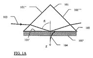
放射検出器であって、
検出される入射放射を吸収し、当該吸収の結果として温度上昇を受ける、エネルギー吸収体と、
エネルギー吸収体の上記温度上昇を検出する光学読取り手段と
を備え、
上記光学読取り手段は、表面プラズモン共鳴を励起することによって光ビームを上記エネルギー吸収体に結合する入力結合手段を含み、表面プラズモン共鳴条件は、エネルギー吸収体の温度に依存し、
上記エネルギー吸収体は、誘電体層によって上記入力結合手段から分離される、
放射検出器によって達成される。
そのようなセンサは、
マイクロメカニカル振動子(より詳細には、カンチレバービームの形をとる)と、
当該マイクロメカニカル振動子の変位を検出する光学読取り手段と
を備え、
当該光学読取り手段は、表面プラズモン共鳴を励起することによって、光ビームを導電性表面に結合する入力結合手段を含み、表面プラズモン共鳴条件は、上記マイクロメカニカル振動子の変位に依存する。
上記マイクロメカニカル振動子は、或る間隙だけ上記入力結合手段から離隔して配置されることができ、上記表面プラズモン共鳴条件は、上記間隙の厚みに依存する。これは、本発明のカンチレバーに基づく熱放射検出器を参照しながら既に説明されているのと同じ動作原理である。
上記入力結合手段は、導電層によって覆われる表面を有する誘電体を含むことができ、当該入力結合手段は、上記導電層内で表面プラズモンを励起するようになっている。
代替的には、上記入力結合手段は、上記間隙によって上記マイクロメカニカル振動子から分離される誘電体表面を有する誘電体を含むことができ、当該マイクロメカニカル振動子は、好ましくは入力結合手段に向かって配置される表面上に導電層を含み、当該入力結合手段は、上記導電層内で表面プラズモンを励起するようになっている。
上記マイクロメカニカル振動子は、環境条件を検知すると共に、当該環境条件に基づく当該マイクロメカニカル振動子の変位又は共振周波数を変更するようになっている、検知層のような、少なくとも1つの検知素子を含むことができる。
上記で説明されたように、上記検知素子は、以下とすることができる:
検出される分子を固着し、それによって、上記マイクロメカニカル振動子の質量又は剛性を変更するか、又はその変位を引き起こすようになっている化学検知素子。
微生物又はその一部を固着し、それによって、上記マイクロメカニカル振動子の質量又は剛性を変更するか、又はその変位を引き起こすようになっている生物検知素子。
電磁界の中に入れられるときに力を受け、それによって、上記マイクロメカニカル振動子の変位を引き起こすようになっている電磁界検知素子。
又は、その温度が基準温度から逸脱するときに熱膨張差を受け、それによって、上記マイクロメカニカル振動子(すなわち、熱放射検出器において用いられる二材料又は多材料ビーム)の変位を引き起こすようになっている熱検知素子。この事例では、センサは、入射放射を吸収し、それによって、上記熱検知素子を加熱するための放射吸収素子をさらに含むことができる。
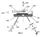
プリズム202の屈折率:1.500
空隙2032の厚み: 500nm
金属層2031:
厚み: 32nm
組成: 銀
デバイ温度: 225K
質量密度: 10.5g/cm2
原子量: 107.87g/mole
抵抗の温度係数: 4100ppm/K
誘電率: −18.2+0.5i
カンチレバー2033:
組成: 金/Si3N4
厚み: 50nm/50nm
ピクセルサイズ: 70μm×10μm
周囲温度: 18℃
この第1のシミュレーションの結果は以下のとおりである。
SPR角θR: 45°30’
熱分解能: 0.013K
エネルギー分解能: 0.001nJ
空隙2032の厚み: 885nm
金属層2031の厚み: 43nm
他の全てのパラメータは変更されていない。
第2のシミュレーションの結果は以下のとおりである。
SPR角θR: 43°23’
熱分解能: 3×10⁻⁴K
エネルギー分解能: 1.8×10⁻⁵nJ
ピクセルサイズ: 25μm×10μm
金属層2031:
厚み: 42nm
組成: 金
デバイ温度: 165K
質量密度: 19.32g/cm2
原子量: 196.97g/mole
抵抗の温度係数: 3800ppm/K
誘電率: −11.54+1.2i
この第3のシミュレーションの結果は以下のとおりである。
SPR角θR: 46°15’
熱分解能: 0.23K
エネルギー分解能: 0.001nJ
プリズム502の屈折率:1.500
空隙5031の厚み: 1010nm
金属層5032:
厚み: 130nm
組成: 銀(第1の例と同じ物理的特性)
ピクセルサイズ: 70μm×10μm
周囲温度: 18℃
この第4のシミュレーションの結果は以下のとおりである。
SPR角θR: 43°28’
熱による反射率の変動: 4%/K
熱分解能: 0.087K
エネルギー分解能: 0.02nJ
空隙5031の厚み: 590nm
金属層5032:
厚み: 130nm
組成: 金(第2の例と同じ物理的特性)
ピクセルサイズ: 25μm×10μm
他の全てのパラメータは第3の例と同じである。
この第5のシミュレーションの結果は以下のとおりである。
SPR角θR: 44°25’
熱による反射率の変動: 3.8%/K
熱分解能: 0.2K
エネルギー分解能: 0.08nJ
Claims (28)
- 放射検出器であって、
検出される入射放射(RAD)を吸収し、該吸収の結果として温度上昇を受ける、エネルギー吸収体(2033、5032)と、
前記エネルギー吸収体(2033、5032)の前記温度上昇を検出する光学読取り手段と
を備え、
前記光学読取り手段は、表面プラズモン共鳴を励起することによって光ビーム(2011、611)を前記エネルギー吸収体(2033、5032)に結合する入力結合手段(202、3021、402、502)を含み、表面プラズモン共鳴条件は、前記エネルギー吸収体(2033、5032)の温度に依存し、
前記エネルギー吸収体(2033、5032)は、誘電体層(2032、5031)によって前記入力結合手段(202、3021、402、502)から分離され、
前記エネルギー吸収体(2033、5032)を前記入力結合手段(202、3021、402、502)から分離する前記誘電体層(2032、5031)は間隙である
ことを特徴とする、放射検出器。 - 前記エネルギー吸収体(2033、5032)と、表面プラズモンをサポートする導電層(2031、402、532)と、前記誘電体層(2032、5031)とを少なくとも含む多層構造(203、403、503)を備える、請求項1記載の放射検出器。
- 前記導電層(2031、402、532)は、金及び銀から選択される材料から形成される、請求項2に記載の放射検出器。
- 前記多層構造(203、403、503)は、前記エネルギー吸収体(2033、5032)の少なくとも一部の温度変動に応じて厚みが変化する誘電体層(2032)を含む、請求項2又は3に記載の放射検出器。
- 前記エネルギー吸収体(2033、5032)は、温度変動に応じて撓むようになっている多材料カンチレバー(2033)をさらに含み、厚みが変化する前記誘電体層(2032)は、前記多材料カンチレバー(2033)を前記入力結合手段(202、3021、402)から分離する前記間隙(2032)を含み、それによって、前記多材料カンチレバー(2033)の撓みが、前記間隙(2032)の幅の変化を引き起こす、請求項1に従属するときの請求項4に記載の放射検出器。
- 前記多材料カンチレバーは二材料カンチレバーである、請求項5に記載の放射検出器。
- 前記多材料カンチレバー(2033)の少なくとも1つの表面(2033’)は、検出される入射放射(RAD)又は粒子束を吸収すると共に、該吸収の結果として、温度上昇を受けるようになっている、請求項5又は6に記載の放射検出器。
- 前記多材料カンチレバー(2033)は誘電体材料のみから形成される、請求項5〜7のいずれか一項に記載の放射検出器。
- 前記入力結合手段(202、3021、402)は、
その上に前記多層構造(203)の導電層(2031)が配置されている、クレッチマン−レーサー構成の誘電体プリズム(202)、
その上に前記多層構造(203)の導電層(2031)が配置されている、誘電体体積格子(3021)、及び
基板(4021)上に配置される導電性レリーフ格子(402)であって、前記エネルギー吸収体の前記多層構造(203)の導電層を構成する導電性レリーフ格子(402)
から選択される、請求項5〜8のいずれか一項に記載の放射検出器。 - 前記間隙(2032)は、
前記多材料カンチレバー(2033)と、
前記誘電体プリズム(202)、体積格子(3021)、又は基板(4021)上に配置される前記導電層(2031)と
の間に配置される、請求項7に記載の放射検出器。 - 前記多層構造(2033、5032)は、前記エネルギー吸収体(2033、5032)の少なくとも一部の温度変動に応じて誘電率が変化する層を含む、請求項1〜10のいずれか一項に記載の放射検出器。
- 温度変動に応じて誘電率が変化する前記層は、前記多材料カンチレバー(2033)の一部である、請求項5〜10のいずれか一項に従属するときの請求項11に記載の放射検出器。
- 誘電率が変化する前記層は、表面プラズモンをサポートする導電層(5032)である、請求項11に記載の放射検出器。
- 誘電率が変化する前記導電層(5032)は、検出される入射放射(RAD)を吸収するようになっていると共に、該吸収の結果として温度上昇を受け、前記誘電体層(5031)によって前記入力結合手段(502)から分離される、請求項13に記載の放射検出器。
- 前記入力結合手段は、オットー構成の誘電体プリズム(502)を含み、該誘電体プリズム(502)と、誘電率が変化する前記導電層(5032)との間に誘電体層(5031)が配置される、請求項13又は14に記載の放射検出器。
- 熱放射検出器の2次元アレイ(600)を含む、請求項1〜15のいずれか一項に記載の放射検出器。
- 前記エネルギー吸収体(2033、5032)の結合面に対して少なくともTM偏光の成分を有する偏光ビーム(2011、611)を生成し、該ビームを、前記エネルギー吸収体(2033、5032)に結合するように前記入力結合手段(202、3021、402、502)に誘導する光放射源(201、601)をさらに備える、請求項1〜16のいずれか一項に記載の放射検出器。
- 前記光放射源(201、601)は可視光放射源又は近赤外線放射源である、請求項17に記載の放射検出器。
- 前記光放射源(201、601)はレーザである、請求項17又は18に記載の放射検出器。
- 前記光ビーム(611)はコリメートされたビームであり、
前記光放射源(601)は、該ビームを前記2次元アレイ(600)の全ての熱放射検出器に同時に誘導するようになっている、請求項16に従属するときの請求項17〜19のいずれか一項に記載の放射検出器。 - 前記入力結合手段によって前記エネルギー吸収体(2033、5032)に結合される前記光ビーム(2011、611)の反射された部分を検出する、光検出器(204)又は光検出器アレイ(604)をさらに備える、請求項1〜20のいずれか一項に記載の放射検出器。
- 前記光検出器(204)又は前記光検出器アレイ(604)は、フォトダイオード、フォトダイオードの2次元アレイ、光電子増倍管、光電子増倍管の2次元アレイ、電荷結合素子、電荷結合素子の2次元アレイ、及び感光性シートから選択される、請求項21に記載の放射検出器。
- 前記反射されたビームを前記放射検出器(204)又は光検出器アレイ(604)に光学的に結合する出力結合手段(202’’’、3022、402、502’’’)をさらに備える、請求項21又は22に記載の放射検出器。
- 前記出力結合手段は、誘電体プリズム(202、502)の1つの表面(202’’’、502’’’)を含み、該プリズムの異なる表面(202’’、502’’)は前記入力結合手段を構成するか、又は該入力結合手段に属する、請求項23に記載の放射検出器。
- 単一の格子(402)が、前記入力結合手段及び前記出力結合手段の両方に属する、請求項23に記載の放射検出器。
- 前記エネルギー吸収体(2033、5032)の温度上昇によって引き起こされる、前記入力結合手段によって前記エネルギー吸収体(2033、5032)に結合される光ビーム(2011、611)の反射された部分の位相の変化を、その強度の変化に変換する干渉手段(205)をさらに備える、請求項1〜25のいずれか一項に記載の放射検出器。
- 前記入力結合手段によって前記エネルギー吸収体(2033、5032)に結合される光ビーム(611)の反射された部分によって搬送される放射像を処理する空間フィルタリング(605)手段をさらに備える、請求項16に従属するときの請求項17〜26のいずれか一項に記載の放射検出器。
- 前記エネルギー吸収体(2033、5032)は、赤外線電磁放射を吸収するようになっている、請求項1〜27のいずれか一項に記載の放射検出器。
Applications Claiming Priority (3)
| Application Number | Priority Date | Filing Date | Title |
|---|---|---|---|
| EP06011321 | 2006-06-01 | ||
| EP06011321.4 | 2006-06-01 | ||
| PCT/EP2007/055068 WO2007137995A2 (en) | 2006-06-01 | 2007-05-24 | A thermal detector |
Publications (2)
| Publication Number | Publication Date |
|---|---|
| JP2009539085A JP2009539085A (ja) | 2009-11-12 |
| JP5384331B2 true JP5384331B2 (ja) | 2014-01-08 |
Family
ID=37264485
Family Applications (1)
| Application Number | Title | Priority Date | Filing Date |
|---|---|---|---|
| JP2009512553A Expired - Fee Related JP5384331B2 (ja) | 2006-06-01 | 2007-05-24 | 表面プラズモン共鳴に基づくセンサ |
Country Status (4)
| Country | Link |
|---|---|
| US (1) | US8242446B2 (ja) |
| EP (1) | EP2029984A2 (ja) |
| JP (1) | JP5384331B2 (ja) |
| WO (1) | WO2007137995A2 (ja) |
Families Citing this family (23)
| Publication number | Priority date | Publication date | Assignee | Title |
|---|---|---|---|---|
| JP2009042164A (ja) * | 2007-08-10 | 2009-02-26 | Hitachi Maxell Ltd | 赤外線カメラ |
| CN101256353B (zh) * | 2008-03-28 | 2010-12-08 | 中国科学院上海光学精密机械研究所 | 探针诱导光刻薄膜及其制备方法 |
| US8159341B2 (en) * | 2008-05-05 | 2012-04-17 | Thorad Corporation | Hazard detection and mitigation system and method |
| FR2965349B1 (fr) * | 2010-09-23 | 2017-01-20 | Commissariat Energie Atomique | Bolometre a detection frequentielle |
| US8461529B2 (en) | 2010-09-23 | 2013-06-11 | Ut-Battelle, Llc | Variable waveband infrared imager |
| US8988061B2 (en) | 2011-02-10 | 2015-03-24 | U.S. Department Of Energy | Nanomechanical electric and electromagnetic field sensor |
| US10965889B2 (en) * | 2011-06-20 | 2021-03-30 | Fluke Corporation | Thermal imager that analyzes temperature measurement calculation accuracy |
| US8569187B2 (en) * | 2011-06-24 | 2013-10-29 | Applied Materials, Inc. | Thermal processing apparatus |
| EP2745096B1 (en) | 2011-08-17 | 2016-10-12 | Public Service Solutions Inc | Passive detectors for imaging systems |
| CN103913244A (zh) * | 2012-12-31 | 2014-07-09 | 中国科学院微电子研究所 | 透明衬底探测器及其制造方法 |
| KR102040149B1 (ko) | 2013-02-01 | 2019-11-04 | 삼성전자주식회사 | 적외선 검출기 |
| KR102040151B1 (ko) | 2013-04-29 | 2019-11-04 | 삼성전자주식회사 | 열 복사 센서 및 이를 포함하는 열상 촬영 장치 |
| CN103398785B (zh) * | 2013-07-26 | 2015-10-28 | 西北核技术研究所 | 基于旋转式吸收体的高能激光能量测量装置 |
| DE102014108424B3 (de) * | 2014-06-16 | 2015-06-11 | Johann Wolfgang Goethe-Universität | Nicht-invasive Stoffanalyse |
| US9851256B2 (en) | 2014-06-26 | 2017-12-26 | MP High Tech Solutions Pty Ltd | Apparatus and method for electromagnetic radiation sensing |
| US9810581B1 (en) | 2014-07-28 | 2017-11-07 | MP High Tech Solutions Pty Ltd | Micromechanical device for electromagnetic radiation sensing |
| US9500468B2 (en) | 2014-08-25 | 2016-11-22 | Board Of Trustees Of Michigan State University | Scanning interferometry technique for through-thickness evaluation in multi-layered transparent structures |
| US9857229B1 (en) | 2015-06-24 | 2018-01-02 | MP High Tech Solutions Pty Ltd | Fabrication method for micromechanical sensors |
| CN109141649B (zh) * | 2018-09-07 | 2023-07-21 | 烯旺新材料科技股份有限公司 | 人体吸收能量的检测装置及其检测方法 |
| US11085878B2 (en) | 2019-06-18 | 2021-08-10 | Eagle Technology, Llc | Radiation detection system with surface plasmon resonance detection and related methods |
| US11009611B2 (en) | 2019-06-18 | 2021-05-18 | Eagle Technology, Llc | Radiation detection system with surface plasmon resonance detection and related methods |
| US11231365B2 (en) * | 2019-07-08 | 2022-01-25 | Hanwha Systems Co., Ltd. | Apparatus and method for infrared imaging |
| KR102267315B1 (ko) * | 2019-12-03 | 2021-06-18 | 고려대학교 산학협력단 | 시료의 입자 크기 측정용 장치 |
Family Cites Families (10)
| Publication number | Priority date | Publication date | Assignee | Title |
|---|---|---|---|---|
| DE4310349C2 (de) * | 1993-03-30 | 2000-11-16 | Inst Mikrotechnik Mainz Gmbh | Sensorkopf und Verfahren zu seiner Herstellung |
| US5929440A (en) | 1996-10-25 | 1999-07-27 | Hypres, Inc. | Electromagnetic radiation detector |
| JPH10267841A (ja) * | 1997-03-24 | 1998-10-09 | Kokuritsu Shintai Shogaisha Rehabilitation Center Souchiyou | 表面プラズモン共鳴センシングデバイス |
| GB9710843D0 (en) | 1997-05-28 | 1997-07-23 | Secr Defence | A thermal detector array |
| EP1088215A1 (en) | 1998-05-26 | 2001-04-04 | California Institute Of Technology | Efficient color display using non-absorbing color filters |
| US6320991B1 (en) * | 1998-10-16 | 2001-11-20 | Imation Corp. | Optical sensor having dielectric film stack |
| US6805839B2 (en) * | 1999-03-12 | 2004-10-19 | Joseph P. Cunningham | Response microcantilever thermal detector |
| US6549687B1 (en) * | 2001-10-26 | 2003-04-15 | Lake Shore Cryotronics, Inc. | System and method for measuring physical, chemical and biological stimuli using vertical cavity surface emitting lasers with integrated tuner |
| US7027676B2 (en) * | 2004-03-08 | 2006-04-11 | Agilent Technologies, Inc. | Optical phase measurement of target |
| NZ528338A (en) | 2004-03-19 | 2006-10-27 | Ind Res Ltd | Biosensors for detecting bond rupture |
-
2007
- 2007-05-24 WO PCT/EP2007/055068 patent/WO2007137995A2/en active Application Filing
- 2007-05-24 JP JP2009512553A patent/JP5384331B2/ja not_active Expired - Fee Related
- 2007-05-24 EP EP07729497A patent/EP2029984A2/en not_active Withdrawn
- 2007-05-24 US US12/227,695 patent/US8242446B2/en not_active Expired - Fee Related
Also Published As
| Publication number | Publication date |
|---|---|
| WO2007137995A2 (en) | 2007-12-06 |
| WO2007137995A3 (en) | 2008-01-31 |
| JP2009539085A (ja) | 2009-11-12 |
| WO2007137995B1 (en) | 2008-03-20 |
| US8242446B2 (en) | 2012-08-14 |
| US20090238236A1 (en) | 2009-09-24 |
| EP2029984A2 (en) | 2009-03-04 |
Similar Documents
| Publication | Publication Date | Title |
|---|---|---|
| JP5384331B2 (ja) | 表面プラズモン共鳴に基づくセンサ | |
| Wachter et al. | Remote optical detection using microcantilevers | |
| US10048200B2 (en) | Optical sensor based with multilayered plasmonic structure comprising a nanoporous metallic layer | |
| US20070279635A1 (en) | Measuring apparatus and method using surface plasmon resonance | |
| Manalis et al. | Two-dimensional micromechanical bimorph arrays for detection of thermal radiation | |
| JP2787960B2 (ja) | 分光測定用の装置 | |
| JP5716977B2 (ja) | 分子共鳴の鏡像力顕微鏡 | |
| Evans et al. | Laser actuation of cantilevers for picometre amplitude dynamic force microscopy | |
| CN101113887A (zh) | 表面等离子共振测量装置和方法 | |
| Hernández et al. | Prism-based surface plasmon resonance for dual-parameter sensing | |
| Papas et al. | Optomechanical metamaterial nanobolometer | |
| JP6025074B2 (ja) | 被測定対象の熱輻射測定装置、及び被測定対象の熱輻射測定方法 | |
| Chen et al. | Oscillating wave sensors based on ultrahigh-order modes in symmetric metal-clad optical waveguides | |
| JPH0949851A (ja) | ワークピースの物理的特性を引き出す方法 | |
| JPH0949849A (ja) | ワークピースのニア・フィールド測定を行うのに適した装置 | |
| Shi et al. | Optical sensitivity analysis of deformed mirrors for microcantilever array IR imaging | |
| KR100911626B1 (ko) | 바이오 센서 측정 장치 | |
| Rosenberger et al. | Impact of silicon nitride thickness on the infrared sensitivity of silicon nitride–aluminum microcantilevers | |
| Michihata et al. | Microdisplacement sensor using an optically trapped microprobe based on the interference scale | |
| Su et al. | A high sensitivity THz detector | |
| Hastanin et al. | A far infrared/terahertz micromechanical sensor based on surface plasmons resonance | |
| Su et al. | A detection technology of THz based on surface plasmon resonance | |
| Hong et al. | Simple nanoimprinted polymer nanostructures for uncooled thermal detection by direct surface plasmon resonance imaging | |
| Higurashi et al. | Nanometer-displacement detection of optically trapped metallic particles based on critical angle method for small force detection | |
| Gotszalk et al. | Parallel SPM cantilever arrays for large area surface metrology and lithography |
Legal Events
| Date | Code | Title | Description |
|---|---|---|---|
| A621 | Written request for application examination |
Free format text: JAPANESE INTERMEDIATE CODE: A621 Effective date: 20100507 |
|
| A131 | Notification of reasons for refusal |
Free format text: JAPANESE INTERMEDIATE CODE: A131 Effective date: 20120417 |
|
| A601 | Written request for extension of time |
Free format text: JAPANESE INTERMEDIATE CODE: A601 Effective date: 20120717 |
|
| A521 | Request for written amendment filed |
Free format text: JAPANESE INTERMEDIATE CODE: A523 Effective date: 20120719 |
|
| A602 | Written permission of extension of time |
Free format text: JAPANESE INTERMEDIATE CODE: A602 Effective date: 20120724 |
|
| A131 | Notification of reasons for refusal |
Free format text: JAPANESE INTERMEDIATE CODE: A131 Effective date: 20130129 |
|
| A521 | Request for written amendment filed |
Free format text: JAPANESE INTERMEDIATE CODE: A523 Effective date: 20130422 |
|
| TRDD | Decision of grant or rejection written | ||
| A01 | Written decision to grant a patent or to grant a registration (utility model) |
Free format text: JAPANESE INTERMEDIATE CODE: A01 Effective date: 20131001 |
|
| A61 | First payment of annual fees (during grant procedure) |
Free format text: JAPANESE INTERMEDIATE CODE: A61 Effective date: 20131002 |
|
| R150 | Certificate of patent or registration of utility model |
Free format text: JAPANESE INTERMEDIATE CODE: R150 |
|
| LAPS | Cancellation because of no payment of annual fees |