JP5376707B2 - Laser annealing equipment - Google Patents
Laser annealing equipment Download PDFInfo
- Publication number
- JP5376707B2 JP5376707B2 JP2008013766A JP2008013766A JP5376707B2 JP 5376707 B2 JP5376707 B2 JP 5376707B2 JP 2008013766 A JP2008013766 A JP 2008013766A JP 2008013766 A JP2008013766 A JP 2008013766A JP 5376707 B2 JP5376707 B2 JP 5376707B2
- Authority
- JP
- Japan
- Prior art keywords
- mirror
- laser
- angle
- deviation
- respect
- Prior art date
- Legal status (The legal status is an assumption and is not a legal conclusion. Google has not performed a legal analysis and makes no representation as to the accuracy of the status listed.)
- Expired - Fee Related
Links
Images


Classifications
-
- B—PERFORMING OPERATIONS; TRANSPORTING
- B23—MACHINE TOOLS; METAL-WORKING NOT OTHERWISE PROVIDED FOR
- B23K—SOLDERING OR UNSOLDERING; WELDING; CLADDING OR PLATING BY SOLDERING OR WELDING; CUTTING BY APPLYING HEAT LOCALLY, e.g. FLAME CUTTING; WORKING BY LASER BEAM
- B23K26/00—Working by laser beam, e.g. welding, cutting or boring
- B23K26/08—Devices involving relative movement between laser beam and workpiece
- B23K26/083—Devices involving movement of the workpiece in at least one axial direction
-
- B—PERFORMING OPERATIONS; TRANSPORTING
- B23—MACHINE TOOLS; METAL-WORKING NOT OTHERWISE PROVIDED FOR
- B23K—SOLDERING OR UNSOLDERING; WELDING; CLADDING OR PLATING BY SOLDERING OR WELDING; CUTTING BY APPLYING HEAT LOCALLY, e.g. FLAME CUTTING; WORKING BY LASER BEAM
- B23K26/00—Working by laser beam, e.g. welding, cutting or boring
- B23K26/02—Positioning or observing the workpiece, e.g. with respect to the point of impact; Aligning, aiming or focusing the laser beam
- B23K26/04—Automatically aligning, aiming or focusing the laser beam, e.g. using the back-scattered light
- B23K26/042—Automatically aligning the laser beam
-
- B—PERFORMING OPERATIONS; TRANSPORTING
- B23—MACHINE TOOLS; METAL-WORKING NOT OTHERWISE PROVIDED FOR
- B23K—SOLDERING OR UNSOLDERING; WELDING; CLADDING OR PLATING BY SOLDERING OR WELDING; CUTTING BY APPLYING HEAT LOCALLY, e.g. FLAME CUTTING; WORKING BY LASER BEAM
- B23K26/00—Working by laser beam, e.g. welding, cutting or boring
- B23K26/02—Positioning or observing the workpiece, e.g. with respect to the point of impact; Aligning, aiming or focusing the laser beam
- B23K26/06—Shaping the laser beam, e.g. by masks or multi-focusing
- B23K26/073—Shaping the laser spot
- B23K26/0738—Shaping the laser spot into a linear shape
Abstract
Description
本発明は、線状ビームを被照射物に照射して被照射物をアニール処理するレーザアニール装置及び方法に関する。 The present invention relates to a laser annealing apparatus and method for annealing an irradiated object by irradiating the irradiated object with a linear beam.
液晶・半導体装置用の薄膜トランジスタの製造工程において、基板(半導体基板またはガラス基板)にレーザビームを照射し基板を改質するためにレーザアニール装置が用いられる。基板の改質には、アモルファスシリコンのような非晶質半導体薄膜の結晶化や、半導体膜に注入した不純物の活性化がある。 In a manufacturing process of a thin film transistor for a liquid crystal / semiconductor device, a laser annealing apparatus is used to modify a substrate by irradiating a substrate (semiconductor substrate or glass substrate) with a laser beam. The substrate modification includes crystallization of an amorphous semiconductor thin film such as amorphous silicon and activation of impurities implanted into the semiconductor film.
図5に、従来のレーザアニール装置30の概略図を示す。レーザアニール装置30は、レーザ発振器31から発振されたレーザビーム32をビーム整形光学系33により線状の断面形状をもつビームに整形し、この線状ビームを被照射物である基板34に対してビーム短軸方向(図でX方向)に走査することにより、基板34上の所望の領域にレーザビームを照射する(例えば、下記特許文献1を参照)。これにより、基板34を改質する。
FIG. 5 shows a schematic diagram of a conventional laser annealing
このようなレーザアニール装置30では、通常、ビーム位置を固定し、基板34を基板ステージ上に載せ、線状ビームの短軸方向に基板を移動させることによりビームの走査が行われる。ここで、レーザビーム32の指向度安定性、位置度安定性はゼロではなく、基準光線に対して出射位置や出射角度がずれる。図5では、角度ずれ光線35及び位置ずれ光線36が模式的に示されている。このような位置ずれ、角度ずれが線状ビームの短軸方向に生じると、被照射面でのビーム位置がビーム短軸方向(X方向)に時間的に往復移動することになる(以下、この現象を「ドリフト」という)。ビーム短軸方向にドリフトが起きると、基板34上の照射領域において、レーザビーム32の照射時間が相対的に長い領域と短い領域とが発生する。
In such a laser annealing
この結果、図6に示すように、目視でも観測できるビーム短軸方向(基板移動方向)に沿った照射ムラが生じる。このムラは数ミリメートル程度の領域で観測されるため、ビームは数秒間というオーダで角度ずれあるいは位置ずれが起きていると考えられる。このようなムラが生じた基板を使って製作される薄膜トランジスタはムラに応じて結晶の品質が異なるため、トランジスタ性能がばらついてしまうという問題がある。 As a result, as shown in FIG. 6, irradiation unevenness occurs along the minor axis direction of the beam (substrate movement direction) that can be observed visually. Since this unevenness is observed in an area of several millimeters, it is considered that the beam is deviated in angle or position on the order of several seconds. A thin film transistor manufactured using a substrate with such unevenness has a problem in that the transistor performance varies because the quality of the crystal varies depending on the unevenness.
このような問題に対し、下記特許文献2では、ドリフトを最小限に抑えるための技術が提案されている。
In order to solve such a problem,
図7に、特許文献2で提案されているレーザ加工装置40のドリフト補正装置41の構成を示す。図7において、ドリフト補正装置41は、光共振器を形成する一対の反射鏡43,44を備えたレーザ発振器42と、レーザ発振器42からのレーザビームを細長い断面形状のビームに変換するビーム整形器51と、ビーム整形器51を通ったビームの幅方向の中心位置を検出するビーム中心位置検出装置(ラインセンサ45,プロファイル位置演算装置46)と、ビームのドリフトにより検出中心位置Pがずれた場合、該ズレΔPをなくすように、光共振器の少なくとも一方の反射鏡の配向θf,θrを変える配向制御機構(ドリフト量演算装置47,ミラー角度演算装置48,リアミラー回転駆動装置49,フロントミラー回転駆動装置50)とを有する。また、図7においてレーザ加工装置40は、レーザビームを整形して基板53の表面に細長い断面形状の線状ビームを集光するためのビームホモジナイザ52を有する。
FIG. 7 shows the configuration of the
このように構成されたドリフト補正装置41により、ラインセンサ45で検出されたビーム中心位置に基づいて、ズレΔPを演算し、このズレΔPをなくすように光共振器の少なくとも一方の反射鏡の配向θf,θrを変える。これにより、基板53の表面におけるレーザビームのドリフトが抑制される。
The
上記特許文献2のドリフト補正装置41では、ビームの中心位置を測定するために、基板照射用のビームホモジナイザ52とは別系統のビーム整形器51を備える必要がある。このため、レーザアニール装置の大型化や製造コストの大幅な増大が避けられない。
また、上記特許文献2のドリフト補正装置41では、光共振器の少なくとも一方の反射鏡の配向を変えるが、このような操作では光共振器内のビームの伝搬特性が変化し、例えばレーザ出力に大きな影響を与えるため、実現性に乏しい。
In the
In addition, in the
本発明は上記の諸問題に鑑みてなされたものであり、新たなビーム整形器を追加することなく、しかも光共振器内のビーム伝搬特性に影響を与えることなく、ビーム短軸方向に生じるドリフトに起因する照射ムラを低減することができるレーザアニール装置及び方法を提供することを課題とする。 The present invention has been made in view of the above-mentioned problems. Drift that occurs in the minor axis direction of the beam without adding a new beam shaper and without affecting the beam propagation characteristics in the optical resonator. It is an object of the present invention to provide a laser annealing apparatus and method that can reduce irradiation unevenness caused by the above.
上記の課題を解決するため、本発明のレーザアニール装置及び方法は、以下の技術的手段を採用する。 In order to solve the above problems, the laser annealing apparatus and method of the present invention employ the following technical means.
本発明は、レーザ発振器から発振されたレーザビームをビーム整形光学系により線状の断面形状をもつビームに整形し、この線状ビームを被照射物に照射して被照射物をアニール処理するレーザアニール装置において、前記ビーム整形光学系を通過する前のレーザビームについて、線状ビームの短軸方向に対応する方向に関しての基準位置からの位置ずれを検出する位置ずれ検出器と、前記ビーム整形光学系を通過する前のレーザビームについて、線状ビームの短軸方向に対応する方向に関しての基準角度からの角度ずれを検出する角度ずれ検出器と、前記レーザ発振器と前記被照射物の間の光路上に配置されレーザビームを偏向させる偏向ミラーと、前記位置ずれ検出器及び前記角度ずれ検出器で検出した検出データに基づいて、被照射面での線状ビームの短軸方向の基準照射位置からの位置ずれをなくすように、前記偏向ミラーの向きを制御するミラー制御手段と、を備えることを特徴とする。 The present invention shapes a laser beam oscillated from a laser oscillator into a beam having a linear cross-sectional shape by a beam shaping optical system, and irradiates the irradiated object with this linear beam to anneal the irradiated object. In the annealing apparatus, for the laser beam before passing through the beam shaping optical system, a position deviation detector for detecting a position deviation from a reference position with respect to a direction corresponding to the minor axis direction of the linear beam, and the beam shaping optics An angle deviation detector for detecting an angle deviation from a reference angle with respect to a direction corresponding to the minor axis direction of the linear beam before passing through the system, and light between the laser oscillator and the irradiated object Based on the deflection mirror arranged on the road and deflecting the laser beam, and the detection data detected by the positional deviation detector and the angular deviation detector To eliminate the positional deviation from the reference irradiation position of the short-axis direction of the linear beam, characterized in that it comprises a mirror control unit for controlling the orientation of the deflection mirror.
また、本発明は、レーザビームをビーム整形光学系により線状の断面形状をもつビームに整形し、この線状ビームを被照射物に照射して被照射物をアニール処理するレーザアニール方法において、前記ビーム整形光学系を通過する前のレーザビームについて、線状ビームの短軸方向に対応する方向に関しての基準位置からの位置ずれと、線状ビームの短軸方向に対応する方向に関しての基準角度からの角度ずれを検出し、検出した位置ずれ及び角度ずれの各ずれ量に基づいて、被照射面での線状ビームの短軸方向の基準照射位置からの位置ずれをなくすように、レーザ発振器と被照射物の間の光路上に配置された偏向ミラーの向きを制御する、ことを特徴とする。 Further, the present invention provides a laser annealing method in which a laser beam is shaped into a beam having a linear cross-sectional shape by a beam shaping optical system, and the irradiated object is irradiated with the linear beam to anneal the irradiated object. The laser beam before passing through the beam shaping optical system is displaced from the reference position with respect to the direction corresponding to the minor axis direction of the linear beam and the reference angle with respect to the direction corresponding to the minor axis direction of the linear beam. The laser oscillator detects the angular deviation from the reference beam and eliminates the positional deviation from the reference irradiation position in the minor axis direction of the linear beam on the irradiated surface based on the detected positional deviation and angular deviation. The direction of the deflecting mirror disposed on the optical path between the object and the object to be irradiated is controlled.
上記のレーザアニール装置及び方法によれば、レーザビームの位置ずれ及び角度ずれを検出し、検出した位置ずれ及び角度ズレの各データに基づいて被照射面での位置ずれをなくすように偏向ミラーの向きを制御する。すなわち、位置ずれ及び角度ずれの各ずれ量に応じて偏向ミラーの向きを変化させ、光線の方向を制御する。これにより、被照射面での位置ずれ(ドリフト)の発生を抑制することができるため、ビーム短軸方向に生じるドリフトに起因する照射ムラを大幅に低減することができる。
また、上記特許文献2の手段と異なり、ビーム整形光学系を通過する前のレーザビームについて位置ずれと角度ずれを検出するので、基板照射用のビームホモジナイザとは別系統のビーム整形器を備える必要がなく、比較的簡単な機器構成で位置ずれと角度ずれを検出することができる。
また、上記特許文献2の手段と異なり、レーザ発振器と被照射物の間の光路上に配置された偏向ミラーを動作させてドリフトを補正するので、光共振器内のビーム伝搬特性に影響を与えることがない。
According to the laser annealing apparatus and method described above, the positional deviation and the angular deviation of the laser beam are detected, and the deflection mirror is arranged so as to eliminate the positional deviation on the irradiated surface based on the detected positional deviation and angular deviation data. Control the orientation. In other words, the direction of the light beam is controlled by changing the direction of the deflecting mirror in accordance with the amount of positional deviation and angular deviation. As a result, the occurrence of misalignment (drift) on the irradiated surface can be suppressed, so that irradiation unevenness due to drift occurring in the beam minor axis direction can be greatly reduced.
Further, unlike the means of the above-mentioned
In addition, unlike the means of the above-mentioned
上記のレーザアニール装置において、好ましくは、前記ミラー制御手段は、前記偏向ミラーを揺動させるミラー駆動装置と、該ミラー駆動装置の動作を制御するミラー角度制御装置とを備え、該ミラー角度制御装置は、前記レーザビームの位置ずれに対する被照射面での基準照射位置からの位置ずれを示す位置用補正テーブル、前記レーザビームの角度ずれに対する被照射面での基準照射位置からの位置ずれを示す角度用補正テーブル及び前記偏向ミラーの配向角度に対する被照射面でのビーム移動量を示すミラー用補正テーブルを記憶しており、前記位置用補正テーブル、前記角度用補正テーブル及び前記ミラー用補正テーブルを用いて、被照射面での線状ビームの短軸方向の位置ずれをなくすための前記偏向ミラーの配向角度を算出する。 In the laser annealing apparatus, preferably, the mirror control unit includes a mirror driving device that swings the deflection mirror, and a mirror angle control device that controls the operation of the mirror driving device, and the mirror angle control device. Is a position correction table indicating a positional deviation from the reference irradiation position on the irradiated surface with respect to the positional deviation of the laser beam, and an angle indicating a positional deviation from the reference irradiation position on the irradiated surface with respect to the angular deviation of the laser beam. Correction table and mirror correction table indicating the amount of beam movement on the irradiated surface with respect to the orientation angle of the deflection mirror are stored, and the position correction table, the angle correction table, and the mirror correction table are used. Calculating the orientation angle of the deflection mirror for eliminating the positional deviation of the linear beam on the irradiated surface in the minor axis direction.
上記構成によれば、ミラー角度制御装置により、位置用補正テーブル、角度用補正テーブル及びミラー用補正テーブルを用いて、被照射面での位置ずれをなくすための偏向ミラーの配向角度が算出されるので、高精度のドリフト補正を行うことができる。 According to the above configuration, the mirror angle control device calculates the orientation angle of the deflection mirror for eliminating the positional deviation on the irradiated surface using the position correction table, the angle correction table, and the mirror correction table. Therefore, highly accurate drift correction can be performed.
上記のレーザアニール装置において、好ましくは、前記偏向ミラーは、前記ビーム整形光学系よりも上流側の光路上に配置されている。 In the laser annealing apparatus, preferably, the deflection mirror is disposed on an optical path upstream of the beam shaping optical system.
ビーム整形光学系よりも上流側の位置では、レーザビームのビーム径は小さいため、当該位置に配置される偏向ミラーは、ビーム整形光学系よりも下流側に配置されるものよりも小型のもので済む。このため、上記の位置に配置された偏向ミラーの配向角度を変える機構を比較的小さく構成することができる。 Since the beam diameter of the laser beam is small at a position upstream of the beam shaping optical system, the deflection mirror disposed at the position is smaller than that disposed downstream of the beam shaping optical system. That's it. For this reason, the mechanism for changing the orientation angle of the deflecting mirror disposed at the above position can be made relatively small.
本発明によれば、新たなビーム整形器を追加することなく、しかも光共振器内のビーム伝搬特性に影響を与えることなく、ビーム短軸方向に生じるドリフトに起因する照射ムラを低減することができる。 According to the present invention, it is possible to reduce irradiation unevenness due to drift occurring in the beam minor axis direction without adding a new beam shaper and without affecting the beam propagation characteristics in the optical resonator. it can.
以下、本発明の好ましい実施形態を添付図面に基づいて詳細に説明する。なお、各図において共通する部分には同一の符号を付し、重複した説明を省略する。 Hereinafter, preferred embodiments of the present invention will be described in detail with reference to the accompanying drawings. In addition, the same code | symbol is attached | subjected to the common part in each figure, and the overlapping description is abbreviate | omitted.
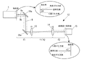
図1は、本発明の実施形態にかかるレーザアニール装置10の全体概略構成を示す図である。
図1において、レーザアニール装置10は、レーザ発振器1と、導入ミラー8と、ビーム整形光学系5と、落射ミラー9と、基板ステージ6とを備える。
FIG. 1 is a diagram showing an overall schematic configuration of a laser annealing
In FIG. 1, the laser annealing
レーザ発振器1は、レーザ媒質2と、光共振器3とを有する。
レーザ媒質2としては、固体レーザ媒質、ガスレーザ媒質、レーザダイオードが例示される。固体レーザ媒質としては、YAG、YLF、YVO4等が例示される。ガスレーザ媒質としては、エキシマ、CO2等が例示される。
光共振器3は、レーザ媒質2の両側に配置された一対の反射鏡3a,3bからなる。後側の反射鏡3aは全反射ミラーであり、出射側の反射鏡3bはハーフミラーである。
上記構成のレーザ発振器1により、一対の反射鏡3a,3bの間で光が増幅されレーザビームBが発振される。レーザビームBは、連続発振ビーム、パルス発振ビームのいずれでもよい。
The
Examples of the
The
The
導入ミラー8は、レーザビームBを偏向する偏向ミラー8a,8bからなり、レーザ発振器1から発振されたレーザビームBをビーム整形光学系5まで導く。
The
ビーム整形光学系5は、レーザ発振器1から発振されたレーザビームBを、被照射面において線状の断面形状をもつビーム(以下、「線状ビームLB」という)に整形する。図1において、線状ビームLBの長軸方向は、紙面に垂直な方向と一致する。
このような線状ビームLBを整形するビーム整形光学系5としては、従来周知の構成を採用することができる。ビーム整形光学系5は、例えば、ビームエキスパンダ、シリンドリカルレンズ、シリンドリカルレンズアレイ等で構成することができる。
The beam shaping
As the beam shaping
また、ビーム整形光学系5は、線状ビームLBの長軸方向のエネルギー分布(光強度分布)を均一化するための長軸用ビームホモジナイザと、線状ビームLBの短軸方向のエネルギー分布を均一化するための短軸用ビームホモジナイザの両方又は一方の機能を備えることが好ましい。この場合、長軸用、短軸用の各ホモジナイザは、シリンドリカルレンズアレイを用いたレンズアレイ方式、導波路を用いた導波路方式、回折光学素子を用いた方式など、各種の形態を採用できる。なお、レンズアレイ方式、導波路方式については例えば特開2007−214527号公報に、回折光学素子については例えば特開2005−217209号公報に開示されている。
Further, the beam shaping
落射ミラー9は、レーザビームBを被照射物である基板7の方向へ反射させる。
基板ステージ6は、基板7を載せる上面を有し、線状ビームLBの短軸方向と一致する図中の矢印X方向に移動可能に構成されている。したがって、基板7を基板ステージ6上に載せて、X方向に移動させることにより、所望の領域に線状ビームLBを走査することができる。
The epi-illumination mirror 9 reflects the laser beam B in the direction of the
The
レーザビームBの被照射物である基板7は、半導体基板又はガラス基板である。半導体基板の場合、イオンが注入された表層部を有し、レーザ照射によって表層部のイオンが活性化される。ガラス基板の場合、表面に非晶質半導体膜(例えばアモルファスシリコン膜)が形成され、レーザ照射によって非晶質半導体膜が結晶性半導体膜に改質される。
The
レーザ発振器1によるレーザビームBの発振や、基板ステージ6の動作は、図示しない制御装置によって制御される。これにより、基板7に対するレーザ照射時間(パルスレーザの場合、照射される単位領域あたりの総照射回数及び総照射時間)が制御される。
The oscillation of the laser beam B by the
図1において、レーザアニール装置10は、さらに、位置ずれ検出器12と、角度ずれ検出器16と、ミラー制御手段(21,22)とを備える。
In FIG. 1, the
位置ずれ検出器12は、ビーム整形光学系5を通過する前のレーザビームBについて、線状ビームLBの短軸方向に対応する方向に関しての基準位置からの位置ずれを検出する。
角度ずれ検出器16は、ビーム整形光学系5を通過する前のレーザビームBについて、線状ビームLBの短軸方向に対応する方向に関しての基準角度からの角度ずれを検出する。
ミラー制御手段(21,22)は、位置ずれ検出器12及び角度ずれ検出器16で検出した検出データに基づいて、被照射面での線状ビームLBの短軸方向の基準照射位置からの位置ずれをなくすように、偏向ミラー8bの向きを制御する。
The
The
Based on the detection data detected by the
図2を参照して、位置ずれ検出器12の一構成例を説明する。ビーム整形光学系5の上流側には、レーザ発振器1から発振されたレーザビームBの一部を分岐するビームスプリッタ19aが設置されており、ビームスプリッタ19aで分岐されたレーザビームBが位置ずれ検出器12に入射する。図2において、ビームスプリッタ19aで分岐されたレーザビームBは偏向ミラー20aで偏向されているが、偏向ミラー20aは位置ずれ検出器12の設置位置によっては省略可能である。
With reference to FIG. 2, a configuration example of the
図2において、破線で示されたBpは実線で示されたレーザビームBを基準光線とした場合の位置ずれ光線のイメージであり、一点鎖線で示されたBaはレーザビームBを基準光線とした場合の角度ずれ光線のイメージである。 In FIG. 2, Bp indicated by a broken line is an image of a misaligned ray when the laser beam B indicated by a solid line is used as a reference ray, and Ba indicated by a one-dot chain line uses the laser beam B as a reference ray. It is an image of an angle-shifted ray in case
図2において、位置ずれ検出器12は、第1焦点距離f1をもつ第1レンズ13と、第2焦点距離f2をもつ第2レンズ14と、位置ずれ検出用の第1撮像装置15とを有する。第1レンズ13は、その主点と物体面(この例では、レーザ発振器1の出射端面)との距離がf1となる位置に配置されている。第2レンズ14は、その主点と第1レンズ13の主点との距離がf1+f2となる位置に配置されている。第1撮像装置15は、その撮像面と第2レンズ14の主点との距離がf2となる位置に配置されている。第1撮像装置15としては、CCDイメージセンサやCMOSイメージセンサが例示される。
In FIG. 2, the
これにより、第1レンズ13と第2レンズ14が像転写光学系を形成し、物体面における像が、第2レンズ14の主点からf2だけ離れた位置の結像面に拡大転写される。このときの拡大倍率は、d1/d2=f1/f2である。第1撮像装置15の撮像面は上記の結像面の位置と一致するので、第1撮像装置15により結像面での転写像を観察することができる。この転写像を観察することで、位置ずれ量は検出されるが、角度ずれ量は検出されない。位置ずれ検出器12で取得した検出データは、ミラー角度制御装置22に送信される。
As a result, the
図3を参照して、角度ずれ検出器16の一構成例を説明する。ビームスプリッタ19aにより分岐されたレーザビームBは、第2レンズ14の出側に設置されたビームスプリッタ19bにより更に分岐されて、角度ずれ検出器16に入射する。図3において、ビームスプリッタ19bにより分岐されたレーザビームBは偏向ミラー20bで偏向されているが、偏向ミラー20bは角度ずれ検出器16の設置位置によっては省略可能である。
With reference to FIG. 3, a configuration example of the
図3において、角度ずれ検出器16は、第1焦点距離f1をもつ第1レンズ13と、第2焦点距離f2をもつ第2レンズ14と、第3焦点距離をもつ第3レンズ17と、角度ずれ検出用の第2撮像装置18とを有する。図3において、角度ずれ検出器16は、第1レンズ13と第2レンズ14を位置ずれ検出器12と共有しているが、位置ずれ検出器12とは独立した第1レンズ13と第2レンズ14を備えても良い。第2撮像装置18は、その撮像面と第3レンズ17の主点との距離が、第3レンズ17の焦点距離であるf3となる位置に配置されている。第2撮像装置18としては、CCDイメージセンサやCMOSイメージセンサが例示される。
In FIG. 3, the
このような構成において、θを角度ずれ量、Daを角度ずれ量θに基づく撮像面での位置ずれ量とした場合、Da=f3・tanθという関係が成立する。したがって、第2撮像装置18により撮像面での位置ずれ量Daを観察することにより、物体面での角度ずれ量θを検出することができる。このとき、位置ずれ量は検出されない。角度ずれ検出器16で取得した検出データは、ミラー角度制御装置22に送信される。
In such a configuration, when θ is an angle shift amount and Da is a position shift amount on the imaging surface based on the angle shift amount θ, the relationship Da = f3 · tan θ is established. Therefore, by observing the positional deviation amount Da on the imaging surface with the
なお、像転写の対象となる物体面の位置は、ビーム整形光学系5より上流側であれば、レーザ発振器1の出射端面に限られない。したがって、上記の物体面の位置は、レーザ発振器1の内部(ただし、出射側の反射鏡3bの外側)でもよいし、偏向ミラー8bの下流側であってもよい。また、上記の物体面の位置をレーザ発振器1の内部に設定する場合、可能であれば、位置ずれ検出器12と角度ずれ検出器16をレーザ発振器1の内部に設置してもよい。
Note that the position of the object surface to be image-transferred is not limited to the emission end surface of the
図1において、ミラー制御手段(21,22)は、偏向ミラーを揺動させるミラー駆動装置21と、ミラー駆動装置21の動作を制御するミラー角度制御装置22とを備える。
偏向ミラー8bは、線状ビームLBの長軸方向と一致する軸心aまわりに揺動自在に支持されている。ミラー駆動装置21は、この偏向ミラー8bに作用してその配向角度を変化させる。ミラー駆動装置21は、例えばACサーボモータで構成することができる。
In FIG. 1, the mirror control means (21, 22) includes a
The
なお、ミラー駆動装置21により揺動させる偏向ミラーは、レーザ発振器1と被照射物である基板7の間の光路上に配置されたものであれば、図1において駆動対象として示されている偏向ミラー8bに限定されない。したがって、別の偏向ミラー8aを揺動させてもよいし、落射ミラー9も偏向ミラーとしての機能を有するから落射ミラー9を揺動させてもよい。
In addition, if the deflection | deviation mirror rock | fluctuated by the
ミラー角度制御装置22は、位置ずれ検出器12と角度ずれ検出器16で検出された検出データに基づいて、被照射面での線状ビームLBの短軸方向の位置ずれをなくすための偏向ミラー8bの配向角度を算出し、算出した配向角度に対応する制御信号をミラー駆動装置21に送信する。
The mirror angle control device 22 is based on the detection data detected by the
図4において、(A)はレーザビームBの位置ずれに対する被照射面での基準照射位置からの位置ずれを示し、(B)はレーザビームBの角度ずれに対する被照射面での基準照射位置からの位置ずれを示し、(C)は偏向ミラーの配向角度に対する被照射面でのビーム移動量を示している。(A)〜(C)は計算あるいは実験により求めることができ、これをテーブル化することで、被照射面での位置ずれをなくすための偏向ミラー8bの配向角度を算出することができる。
4A shows the positional deviation from the reference irradiation position on the irradiated surface with respect to the positional deviation of the laser beam B, and FIG. 4B shows the positional deviation from the reference irradiation position on the irradiated surface with respect to the angular deviation of the laser beam B. (C) shows the amount of beam movement on the irradiated surface with respect to the orientation angle of the deflection mirror. (A) to (C) can be obtained by calculation or experiment, and by making this a table, it is possible to calculate the orientation angle of the
具体的には、ミラー角度制御装置22は、レーザビームBの位置ずれに対する被照射面での基準照射位置からの位置ずれを示す位置用補正テーブル、レーザビームBの角度ずれに対する被照射面での基準照射位置からの位置ずれを示す角度用補正テーブル及び偏向ミラーの配向角度に対する被照射面でのビーム移動量を示すミラー用補正テーブルを記憶しており、位置用補正テーブル、角度用補正テーブル及びミラー用補正テーブルを用いて、被照射面での線状ビームLBの短軸方向の位置ずれをなくすための偏向ミラー8bの配向角度を算出する。さらに、ミラー角度制御装置22は、算出した配向角度に対応する制御信号をミラー駆動装置21に送信する。
Specifically, the mirror angle control device 22 includes a position correction table indicating a positional deviation from the reference irradiation position on the irradiated surface with respect to the positional deviation of the laser beam B, and an irradiation surface with respect to the angular deviation of the laser beam B. An angle correction table that indicates a positional deviation from the reference irradiation position and a mirror correction table that indicates the amount of beam movement on the irradiated surface with respect to the orientation angle of the deflection mirror are stored, and a position correction table, an angle correction table, and Using the mirror correction table, the orientation angle of the
ミラー駆動装置21は、ミラー角度制御装置22からの制御信号に従って偏向ミラー8bの配向角度を変化させる。
上記の構成により、レーザビームBの位置ずれ及び角度ずれをリアルタイムで検出し、偏向ミラー8bの配向角度を自動制御するので、被照射面でのドリフト補正をリアルタイムで実行することができる。
The
With the above configuration, the positional deviation and the angular deviation of the laser beam B are detected in real time, and the orientation angle of the
上述した本発明のレーザアニール装置10及び方法によれば、位置ずれ及び角度ずれの各ずれ量に応じて偏向ミラー8bの向きを変化させ、偏向ミラー8b以降のレーザビームBの方向を制御する。これにより、被照射面での位置ずれ(ドリフト)の発生を抑制することができるため、ビーム短軸方向に生じるドリフトに起因する照射ムラを大幅に低減することができる。
According to the
また、上記特許文献2の手段と異なり、ビーム整形光学系5を通過する前のレーザビームBについて位置ずれと角度ずれを検出するので、基板照射用のビームホモジナイザ(実施形態ではビーム整形光学系5)とは別系統のビーム整形器を備える必要がなく、比較的簡単な機器構成で位置ずれと角度ずれを検出することができる。
Further, unlike the means of the above-mentioned
また、上記特許文献2の手段と異なり、レーザ発振器1と被照射物である基板7の間の光路上に配置された偏向ミラー8bを動作させてドリフトを補正するので、光共振器3内のビーム伝搬特性に影響を与えることがない。
Further, unlike the means of the above-mentioned
また、本実施形態によれば、ミラー角度制御装置22により、位置用補正テーブル、角度用補正テーブル及びミラー用補正テーブルを用いて、被照射面での位置ずれをなくすための偏向ミラー8bの配向角度が算出されるので、高精度のドリフト補正を行うことができる。
Further, according to the present embodiment, the mirror angle control device 22 uses the position correction table, the angle correction table, and the mirror correction table to align the
また、本実施形態によれば、ビーム整形光学系5よりも上流側の光路上に配置された偏向ミラー8bを揺動させる構成を採用している。ビーム整形光学系5よりも上流側の位置では、レーザビームBのビーム径は小さいため、この位置に配置される偏向ミラーは、ビーム整形光学系5よりも下流側に配置されるミラー(本実施形態では落射ミラー9)よりも小型である。したがって、ミラー駆動装置21を比較的小さく構成することができる。
In addition, according to the present embodiment, a configuration is adopted in which the
なお、上述した実施形態では、ビーム照射位置を固定し、基板7をビーム短軸方向に移動させることにより、ビーム走査を行う構成であったが、このような構成に代えて、基板位置を固定し、ビームを短軸方向に振ることにより、ビーム走査を行う構成を採用していてもよい。この場合、例えば特開2003−45820に開示されているように、ガルバノスキャナまたはポリゴンミラーと、fθレンズとの組み合わせによってビーム短軸方向にビームを振る手段を構成することができる。
In the above-described embodiment, the beam irradiation position is fixed and the
上記において、本発明の実施形態について説明を行ったが、上記に開示された本発明の実施の形態は、あくまで例示であって、本発明の範囲はこれら発明の実施の形態に限定されない。本発明の範囲は、特許請求の範囲の記載によって示され、さらに特許請求の範囲の記載と均等の意味および範囲内でのすべての変更を含むものである。 Although the embodiments of the present invention have been described above, the embodiments of the present invention disclosed above are merely examples, and the scope of the present invention is not limited to these embodiments. The scope of the present invention is indicated by the description of the scope of claims, and further includes meanings equivalent to the description of the scope of claims and all modifications within the scope.
B レーザビーム
LB 線状ビーム
1 レーザ発振器
2 レーザ媒質
3 光共振器
3a,3b 反射鏡
5 ビーム整形光学系
6 基板ステージ
7 基板(被照射物)
8 導入ミラー
8a,8b 偏向ミラー
9 落射ミラー
10 レーザアニール装置
12 位置ずれ検出器
13 第1レンズ
14 第2レンズ
15 第1撮像装置
16 角度ずれ検出器
17 第3レンズ
18 第2撮像装置
19a,19b ビームスプリッタ
20a,20b 偏向ミラー
21 ミラー駆動装置
22 ミラー角度制御装置
B Laser beam
8 Introducing
Claims (2)
前記ビーム整形光学系を通過する前のレーザビームについて、前記線状ビームの短軸方向に対応する方向に関しての基準位置からの位置ずれを検出する位置ずれ検出器と、
前記ビーム整形光学系を通過する前のレーザビームについて、前記線状ビームの短軸方向に対応する方向に関しての基準角度からの角度ずれを検出する角度ずれ検出器と、
前記レーザ発振器と前記被照射物の間の光路上に配置され前記レーザビームを偏向させる偏向ミラーと、
前記位置ずれ検出器及び前記角度ずれ検出器で検出した検出データに基づいて、被照射面での前記線状ビームの短軸方向の基準照射位置からの位置ずれをなくすように、前記偏向ミラーの向きを制御するミラー制御手段と、
を備えるレーザアニール装置であって、
前記ミラー制御手段は、前記偏向ミラーを揺動させるミラー駆動装置と、該ミラー駆動装置の動作を制御するミラー角度制御装置とを備え、
該ミラー角度制御装置は、前記レーザビームの位置ずれに対する被照射面での基準照射位置からの位置ずれを示す位置用補正テーブル、前記レーザビームの角度ずれに対する被照射面での基準照射位置からの位置ずれを示す角度用補正テーブル及び前記偏向ミラーの配向角度に対する被照射面でのビーム移動量を示すミラー用補正テーブルを記憶しており、前記位置用補正テーブル、前記角度用補正テーブル及び前記ミラー用補正テーブルを用いて、被照射面での線状ビームの短軸方向の位置ずれをなくすための前記偏向ミラーの配向角度を算出することを特徴とするレーザアニール装置。 In a laser annealing apparatus for shaping a laser beam oscillated from a laser oscillator into a beam having a linear cross-sectional shape by a beam shaping optical system, and irradiating the irradiated object with the linear beam to anneal the irradiated object ,
A misregistration detector that detects a misregistration from a reference position with respect to a direction corresponding to a minor axis direction of the linear beam with respect to the laser beam before passing through the beam shaping optical system;
An angle deviation detector for detecting an angle deviation from a reference angle with respect to a direction corresponding to a minor axis direction of the linear beam with respect to the laser beam before passing through the beam shaping optical system;
A deflection mirror disposed on an optical path between the laser oscillator and the irradiated object to deflect the laser beam;
Based on the detection data detected by the misalignment detector and the angular misalignment detector, the deflection mirror is arranged so as to eliminate misalignment from the reference irradiation position in the short axis direction of the linear beam on the irradiated surface. Mirror control means for controlling the orientation;
A Relais Zaaniru apparatus provided with,
The mirror control means includes a mirror drive device that swings the deflection mirror, and a mirror angle control device that controls the operation of the mirror drive device,
The mirror angle control device includes a position correction table that indicates a positional deviation from a reference irradiation position on the irradiated surface with respect to a positional deviation of the laser beam, and a reference irradiation position on the irradiated surface with respect to an angular deviation of the laser beam. An angle correction table that indicates positional deviation and a mirror correction table that indicates the amount of beam movement on the irradiated surface with respect to the orientation angle of the deflection mirror are stored. The position correction table, the angle correction table, and the mirror A laser annealing apparatus for calculating an orientation angle of the deflecting mirror for eliminating a positional deviation of a linear beam in a minor axis direction on an irradiated surface using a correction table.
Priority Applications (2)
| Application Number | Priority Date | Filing Date | Title |
|---|---|---|---|
| JP2008013766A JP5376707B2 (en) | 2008-01-24 | 2008-01-24 | Laser annealing equipment |
| US12/355,871 US8106341B2 (en) | 2008-01-24 | 2009-01-19 | Laser annealing apparatus and method |
Applications Claiming Priority (1)
| Application Number | Priority Date | Filing Date | Title |
|---|---|---|---|
| JP2008013766A JP5376707B2 (en) | 2008-01-24 | 2008-01-24 | Laser annealing equipment |
Publications (3)
| Publication Number | Publication Date |
|---|---|
| JP2009176934A JP2009176934A (en) | 2009-08-06 |
| JP2009176934A5 JP2009176934A5 (en) | 2011-02-24 |
| JP5376707B2 true JP5376707B2 (en) | 2013-12-25 |
Family
ID=41012444
Family Applications (1)
| Application Number | Title | Priority Date | Filing Date |
|---|---|---|---|
| JP2008013766A Expired - Fee Related JP5376707B2 (en) | 2008-01-24 | 2008-01-24 | Laser annealing equipment |
Country Status (2)
| Country | Link |
|---|---|
| US (1) | US8106341B2 (en) |
| JP (1) | JP5376707B2 (en) |
Families Citing this family (19)
| Publication number | Priority date | Publication date | Assignee | Title |
|---|---|---|---|---|
| USRE46672E1 (en) | 2006-07-13 | 2018-01-16 | Velodyne Lidar, Inc. | High definition LiDAR system |
| CN102513701B (en) | 2008-01-07 | 2015-08-19 | 株式会社Ihi | Laser anneal method and device |
| US8115137B2 (en) * | 2008-06-12 | 2012-02-14 | Ihi Corporation | Laser annealing method and laser annealing apparatus |
| JP5316124B2 (en) * | 2009-03-13 | 2013-10-16 | 日産自動車株式会社 | Laser welding equipment |
| US8669507B2 (en) * | 2010-10-22 | 2014-03-11 | Industrial Technology Research Institute | Laser scanning device |
| US20120097833A1 (en) * | 2010-10-22 | 2012-04-26 | Industrial Technology Research Institute | Laser scanning device |
| US10627490B2 (en) | 2016-01-31 | 2020-04-21 | Velodyne Lidar, Inc. | Multiple pulse, LIDAR based 3-D imaging |
| CA3017735C (en) | 2016-03-19 | 2023-03-14 | Velodyne Lidar, Inc. | Integrated illumination and detection for lidar based 3-d imaging |
| US10804407B2 (en) | 2016-05-12 | 2020-10-13 | Semiconductor Energy Laboratory Co., Ltd. | Laser processing apparatus and stack processing apparatus |
| JP7165587B2 (en) | 2016-06-01 | 2022-11-04 | ベロダイン ライダー ユーエスエー,インコーポレイテッド | Multi-pixel scanning LIDAR |
| KR102603393B1 (en) * | 2016-12-06 | 2023-11-17 | 삼성디스플레이 주식회사 | Laser processing apparatus |
| JP6496340B2 (en) * | 2017-03-17 | 2019-04-03 | ファナック株式会社 | Scanner control device, robot control device, and remote laser welding robot system |
| US10386465B2 (en) | 2017-03-31 | 2019-08-20 | Velodyne Lidar, Inc. | Integrated LIDAR illumination power control |
| US10545222B2 (en) | 2017-05-08 | 2020-01-28 | Velodyne Lidar, Inc. | LIDAR data acquisition and control |
| US11294041B2 (en) | 2017-12-08 | 2022-04-05 | Velodyne Lidar Usa, Inc. | Systems and methods for improving detection of a return signal in a light ranging and detection system |
| US10712434B2 (en) | 2018-09-18 | 2020-07-14 | Velodyne Lidar, Inc. | Multi-channel LIDAR illumination driver |
| US11082010B2 (en) | 2018-11-06 | 2021-08-03 | Velodyne Lidar Usa, Inc. | Systems and methods for TIA base current detection and compensation |
| US11885958B2 (en) | 2019-01-07 | 2024-01-30 | Velodyne Lidar Usa, Inc. | Systems and methods for a dual axis resonant scanning mirror |
| US10613203B1 (en) | 2019-07-01 | 2020-04-07 | Velodyne Lidar, Inc. | Interference mitigation for light detection and ranging |
Family Cites Families (17)
| Publication number | Priority date | Publication date | Assignee | Title |
|---|---|---|---|---|
| US4504147A (en) * | 1981-07-28 | 1985-03-12 | Huang Cheng Chung | Angular alignment sensor |
| JPH0373914A (en) * | 1989-08-16 | 1991-03-28 | Toshiba Corp | Optical axis adjusting device |
| JP3248109B2 (en) * | 1990-11-02 | 2002-01-21 | ソニー株式会社 | Step and repeat laser crystallization method and laser beam irradiation method |
| JPH11162868A (en) * | 1997-12-02 | 1999-06-18 | Toshiba Corp | Laser irradiation device |
| JPH11251220A (en) * | 1998-03-02 | 1999-09-17 | Nikon Corp | Exposure equipment and exposure method |
| JP2000042777A (en) | 1998-07-29 | 2000-02-15 | Sumitomo Heavy Ind Ltd | Device and method of correcting drift of laser beam and laser beam machine using this device |
| JP4180718B2 (en) * | 1999-01-29 | 2008-11-12 | 株式会社トプコン | Rotating laser device |
| JP2001102323A (en) * | 1999-09-30 | 2001-04-13 | Matsushita Electric Ind Co Ltd | Method for manufacturing laser-annealing apparatus and thin-film |
| JP2002158186A (en) | 2000-11-21 | 2002-05-31 | Toshiba Corp | Method and apparatus for laser annealing |
| JP2003045820A (en) | 2001-07-30 | 2003-02-14 | Semiconductor Energy Lab Co Ltd | Laser irradiation apparatus, and method, and method of manufacturing semiconductor device |
| JP3947065B2 (en) | 2002-08-30 | 2007-07-18 | 住友重機械工業株式会社 | Uniform laser beam irradiation device |
| JP2005217209A (en) * | 2004-01-30 | 2005-08-11 | Hitachi Ltd | Laser annealing method and laser annealer |
| JP4567984B2 (en) * | 2004-01-30 | 2010-10-27 | 株式会社 日立ディスプレイズ | Flat panel display manufacturing equipment |
| JP2006287183A (en) | 2005-03-10 | 2006-10-19 | Ishikawajima Harima Heavy Ind Co Ltd | Laser irradiation equipment of laser annealing device |
| JP2007110064A (en) | 2005-09-14 | 2007-04-26 | Ishikawajima Harima Heavy Ind Co Ltd | Laser annealing method and device thereof |
| JP2007214527A (en) | 2006-01-13 | 2007-08-23 | Ihi Corp | Laser annealing method and laser annealer |
| KR100828367B1 (en) * | 2006-08-28 | 2008-05-08 | 삼성전자주식회사 | Laser displasy apparatus |
-
2008
- 2008-01-24 JP JP2008013766A patent/JP5376707B2/en not_active Expired - Fee Related
-
2009
- 2009-01-19 US US12/355,871 patent/US8106341B2/en active Active
Also Published As
| Publication number | Publication date |
|---|---|
| US20090218475A1 (en) | 2009-09-03 |
| JP2009176934A (en) | 2009-08-06 |
| US8106341B2 (en) | 2012-01-31 |
Similar Documents
| Publication | Publication Date | Title |
|---|---|---|
| JP5376707B2 (en) | Laser annealing equipment | |
| WO2009150733A1 (en) | Laser annealing method and laser annealing apparatus | |
| KR100711155B1 (en) | Apparatus for manufacturing flat panel display devices | |
| JP6353683B2 (en) | Laser processing apparatus and laser processing method | |
| JP5254761B2 (en) | Laser processing equipment | |
| KR101242094B1 (en) | Laser anneal method and device | |
| US7991037B2 (en) | Multi-beam laser apparatus | |
| US7333255B2 (en) | Laser processing device | |
| KR100755817B1 (en) | Method and apparatus for correcting a defective pixel of a liquid crystal display | |
| KR20130138686A (en) | Laser annealing systems and methods with ultra-short dwell times | |
| JP2010530614A (en) | System and method for processing semiconductor structures using laser pulses distributed laterally within a scan window | |
| JPWO2008053915A1 (en) | Scanner optical system, laser processing apparatus, and scanner optical apparatus | |
| JP2006196638A (en) | Laser oscillation control method of pulse laser, and pulse laser system | |
| US20190193197A1 (en) | Laser machining apparatus and laser machining method | |
| JP5120685B2 (en) | Laser annealing method and laser annealing apparatus | |
| KR20130077415A (en) | Laser annealing appratus and laser annealing method | |
| JP2003347236A (en) | Laser irradiation device | |
| KR20200028601A (en) | Laser system and method for maintaining laser path | |
| JP5021277B2 (en) | Laser processing equipment | |
| JP7308439B2 (en) | LASER PROCESSING DEVICE AND OPTICAL ADJUSTMENT METHOD | |
| JP7262081B2 (en) | LASER PROCESSING DEVICE AND OPTICAL ADJUSTMENT METHOD | |
| KR20170039815A (en) | Laser crystalling apparatus | |
| JP2011044502A (en) | Light irradiation device and annealing device | |
| JP2009039733A (en) | Laser beam machining apparatus | |
| US20220084823A1 (en) | Laser irradiation apparatus and laser irradiation method |
Legal Events
| Date | Code | Title | Description |
|---|---|---|---|
| A521 | Request for written amendment filed |
Free format text: JAPANESE INTERMEDIATE CODE: A523 Effective date: 20110110 |
|
| A621 | Written request for application examination |
Free format text: JAPANESE INTERMEDIATE CODE: A621 Effective date: 20110110 |
|
| A131 | Notification of reasons for refusal |
Free format text: JAPANESE INTERMEDIATE CODE: A131 Effective date: 20130702 |
|
| A521 | Request for written amendment filed |
Free format text: JAPANESE INTERMEDIATE CODE: A523 Effective date: 20130715 |
|
| TRDD | Decision of grant or rejection written | ||
| A01 | Written decision to grant a patent or to grant a registration (utility model) |
Free format text: JAPANESE INTERMEDIATE CODE: A01 Effective date: 20130917 |
|
| A61 | First payment of annual fees (during grant procedure) |
Free format text: JAPANESE INTERMEDIATE CODE: A61 Effective date: 20130923 |
|
| R150 | Certificate of patent or registration of utility model |
Ref document number: 5376707 Country of ref document: JP Free format text: JAPANESE INTERMEDIATE CODE: R150 Free format text: JAPANESE INTERMEDIATE CODE: R150 |
|
| R250 | Receipt of annual fees |
Free format text: JAPANESE INTERMEDIATE CODE: R250 |
|
| R250 | Receipt of annual fees |
Free format text: JAPANESE INTERMEDIATE CODE: R250 |
|
| R250 | Receipt of annual fees |
Free format text: JAPANESE INTERMEDIATE CODE: R250 |
|
| LAPS | Cancellation because of no payment of annual fees |