JP5358105B2 - Display device - Google Patents
Display device Download PDFInfo
- Publication number
- JP5358105B2 JP5358105B2 JP2008060359A JP2008060359A JP5358105B2 JP 5358105 B2 JP5358105 B2 JP 5358105B2 JP 2008060359 A JP2008060359 A JP 2008060359A JP 2008060359 A JP2008060359 A JP 2008060359A JP 5358105 B2 JP5358105 B2 JP 5358105B2
- Authority
- JP
- Japan
- Prior art keywords
- voltage
- film
- signal line
- video signal
- transistor
- Prior art date
- Legal status (The legal status is an assumption and is not a legal conclusion. Google has not performed a legal analysis and makes no representation as to the accuracy of the status listed.)
- Expired - Fee Related
Links
Images


Classifications
-
- G—PHYSICS
- G09—EDUCATION; CRYPTOGRAPHY; DISPLAY; ADVERTISING; SEALS
- G09G—ARRANGEMENTS OR CIRCUITS FOR CONTROL OF INDICATING DEVICES USING STATIC MEANS TO PRESENT VARIABLE INFORMATION
- G09G3/00—Control arrangements or circuits, of interest only in connection with visual indicators other than cathode-ray tubes
- G09G3/20—Control arrangements or circuits, of interest only in connection with visual indicators other than cathode-ray tubes for presentation of an assembly of a number of characters, e.g. a page, by composing the assembly by combination of individual elements arranged in a matrix no fixed position being assigned to or needed to be assigned to the individual characters or partial characters
- G09G3/34—Control arrangements or circuits, of interest only in connection with visual indicators other than cathode-ray tubes for presentation of an assembly of a number of characters, e.g. a page, by composing the assembly by combination of individual elements arranged in a matrix no fixed position being assigned to or needed to be assigned to the individual characters or partial characters by control of light from an independent source
- G09G3/36—Control arrangements or circuits, of interest only in connection with visual indicators other than cathode-ray tubes for presentation of an assembly of a number of characters, e.g. a page, by composing the assembly by combination of individual elements arranged in a matrix no fixed position being assigned to or needed to be assigned to the individual characters or partial characters by control of light from an independent source using liquid crystals
- G09G3/3611—Control of matrices with row and column drivers
- G09G3/3648—Control of matrices with row and column drivers using an active matrix
-
- G—PHYSICS
- G09—EDUCATION; CRYPTOGRAPHY; DISPLAY; ADVERTISING; SEALS
- G09G—ARRANGEMENTS OR CIRCUITS FOR CONTROL OF INDICATING DEVICES USING STATIC MEANS TO PRESENT VARIABLE INFORMATION
- G09G3/00—Control arrangements or circuits, of interest only in connection with visual indicators other than cathode-ray tubes
- G09G3/20—Control arrangements or circuits, of interest only in connection with visual indicators other than cathode-ray tubes for presentation of an assembly of a number of characters, e.g. a page, by composing the assembly by combination of individual elements arranged in a matrix no fixed position being assigned to or needed to be assigned to the individual characters or partial characters
- G09G3/34—Control arrangements or circuits, of interest only in connection with visual indicators other than cathode-ray tubes for presentation of an assembly of a number of characters, e.g. a page, by composing the assembly by combination of individual elements arranged in a matrix no fixed position being assigned to or needed to be assigned to the individual characters or partial characters by control of light from an independent source
- G09G3/36—Control arrangements or circuits, of interest only in connection with visual indicators other than cathode-ray tubes for presentation of an assembly of a number of characters, e.g. a page, by composing the assembly by combination of individual elements arranged in a matrix no fixed position being assigned to or needed to be assigned to the individual characters or partial characters by control of light from an independent source using liquid crystals
-
- G—PHYSICS
- G02—OPTICS
- G02F—OPTICAL DEVICES OR ARRANGEMENTS FOR THE CONTROL OF LIGHT BY MODIFICATION OF THE OPTICAL PROPERTIES OF THE MEDIA OF THE ELEMENTS INVOLVED THEREIN; NON-LINEAR OPTICS; FREQUENCY-CHANGING OF LIGHT; OPTICAL LOGIC ELEMENTS; OPTICAL ANALOGUE/DIGITAL CONVERTERS
- G02F1/00—Devices or arrangements for the control of the intensity, colour, phase, polarisation or direction of light arriving from an independent light source, e.g. switching, gating or modulating; Non-linear optics
- G02F1/01—Devices or arrangements for the control of the intensity, colour, phase, polarisation or direction of light arriving from an independent light source, e.g. switching, gating or modulating; Non-linear optics for the control of the intensity, phase, polarisation or colour
- G02F1/13—Devices or arrangements for the control of the intensity, colour, phase, polarisation or direction of light arriving from an independent light source, e.g. switching, gating or modulating; Non-linear optics for the control of the intensity, phase, polarisation or colour based on liquid crystals, e.g. single liquid crystal display cells
- G02F1/133—Constructional arrangements; Operation of liquid crystal cells; Circuit arrangements
-
- G—PHYSICS
- G09—EDUCATION; CRYPTOGRAPHY; DISPLAY; ADVERTISING; SEALS
- G09G—ARRANGEMENTS OR CIRCUITS FOR CONTROL OF INDICATING DEVICES USING STATIC MEANS TO PRESENT VARIABLE INFORMATION
- G09G3/00—Control arrangements or circuits, of interest only in connection with visual indicators other than cathode-ray tubes
- G09G3/20—Control arrangements or circuits, of interest only in connection with visual indicators other than cathode-ray tubes for presentation of an assembly of a number of characters, e.g. a page, by composing the assembly by combination of individual elements arranged in a matrix no fixed position being assigned to or needed to be assigned to the individual characters or partial characters
-
- G—PHYSICS
- G09—EDUCATION; CRYPTOGRAPHY; DISPLAY; ADVERTISING; SEALS
- G09G—ARRANGEMENTS OR CIRCUITS FOR CONTROL OF INDICATING DEVICES USING STATIC MEANS TO PRESENT VARIABLE INFORMATION
- G09G2310/00—Command of the display device
- G09G2310/06—Details of flat display driving waveforms
-
- G—PHYSICS
- G09—EDUCATION; CRYPTOGRAPHY; DISPLAY; ADVERTISING; SEALS
- G09G—ARRANGEMENTS OR CIRCUITS FOR CONTROL OF INDICATING DEVICES USING STATIC MEANS TO PRESENT VARIABLE INFORMATION
- G09G2310/00—Command of the display device
- G09G2310/08—Details of timing specific for flat panels, other than clock recovery
-
- G—PHYSICS
- G09—EDUCATION; CRYPTOGRAPHY; DISPLAY; ADVERTISING; SEALS
- G09G—ARRANGEMENTS OR CIRCUITS FOR CONTROL OF INDICATING DEVICES USING STATIC MEANS TO PRESENT VARIABLE INFORMATION
- G09G2320/00—Control of display operating conditions
- G09G2320/04—Maintaining the quality of display appearance
- G09G2320/043—Preventing or counteracting the effects of ageing
-
- G—PHYSICS
- G09—EDUCATION; CRYPTOGRAPHY; DISPLAY; ADVERTISING; SEALS
- G09G—ARRANGEMENTS OR CIRCUITS FOR CONTROL OF INDICATING DEVICES USING STATIC MEANS TO PRESENT VARIABLE INFORMATION
- G09G3/00—Control arrangements or circuits, of interest only in connection with visual indicators other than cathode-ray tubes
- G09G3/20—Control arrangements or circuits, of interest only in connection with visual indicators other than cathode-ray tubes for presentation of an assembly of a number of characters, e.g. a page, by composing the assembly by combination of individual elements arranged in a matrix no fixed position being assigned to or needed to be assigned to the individual characters or partial characters
- G09G3/2007—Display of intermediate tones
- G09G3/2018—Display of intermediate tones by time modulation using two or more time intervals
- G09G3/2022—Display of intermediate tones by time modulation using two or more time intervals using sub-frames
-
- G—PHYSICS
- G09—EDUCATION; CRYPTOGRAPHY; DISPLAY; ADVERTISING; SEALS
- G09G—ARRANGEMENTS OR CIRCUITS FOR CONTROL OF INDICATING DEVICES USING STATIC MEANS TO PRESENT VARIABLE INFORMATION
- G09G3/00—Control arrangements or circuits, of interest only in connection with visual indicators other than cathode-ray tubes
- G09G3/20—Control arrangements or circuits, of interest only in connection with visual indicators other than cathode-ray tubes for presentation of an assembly of a number of characters, e.g. a page, by composing the assembly by combination of individual elements arranged in a matrix no fixed position being assigned to or needed to be assigned to the individual characters or partial characters
- G09G3/34—Control arrangements or circuits, of interest only in connection with visual indicators other than cathode-ray tubes for presentation of an assembly of a number of characters, e.g. a page, by composing the assembly by combination of individual elements arranged in a matrix no fixed position being assigned to or needed to be assigned to the individual characters or partial characters by control of light from an independent source
- G09G3/36—Control arrangements or circuits, of interest only in connection with visual indicators other than cathode-ray tubes for presentation of an assembly of a number of characters, e.g. a page, by composing the assembly by combination of individual elements arranged in a matrix no fixed position being assigned to or needed to be assigned to the individual characters or partial characters by control of light from an independent source using liquid crystals
- G09G3/3611—Control of matrices with row and column drivers
- G09G3/3614—Control of polarity reversal in general
-
- G—PHYSICS
- G09—EDUCATION; CRYPTOGRAPHY; DISPLAY; ADVERTISING; SEALS
- G09G—ARRANGEMENTS OR CIRCUITS FOR CONTROL OF INDICATING DEVICES USING STATIC MEANS TO PRESENT VARIABLE INFORMATION
- G09G3/00—Control arrangements or circuits, of interest only in connection with visual indicators other than cathode-ray tubes
- G09G3/20—Control arrangements or circuits, of interest only in connection with visual indicators other than cathode-ray tubes for presentation of an assembly of a number of characters, e.g. a page, by composing the assembly by combination of individual elements arranged in a matrix no fixed position being assigned to or needed to be assigned to the individual characters or partial characters
- G09G3/34—Control arrangements or circuits, of interest only in connection with visual indicators other than cathode-ray tubes for presentation of an assembly of a number of characters, e.g. a page, by composing the assembly by combination of individual elements arranged in a matrix no fixed position being assigned to or needed to be assigned to the individual characters or partial characters by control of light from an independent source
- G09G3/36—Control arrangements or circuits, of interest only in connection with visual indicators other than cathode-ray tubes for presentation of an assembly of a number of characters, e.g. a page, by composing the assembly by combination of individual elements arranged in a matrix no fixed position being assigned to or needed to be assigned to the individual characters or partial characters by control of light from an independent source using liquid crystals
- G09G3/3611—Control of matrices with row and column drivers
- G09G3/3696—Generation of voltages supplied to electrode drivers
Abstract
Description
本発明は、アクティブマトリクス型の表示装置、及びその駆動方法に関する。 The present invention relates to an active matrix display device and a driving method thereof.
アクティブマトリクス型の表示装置は、マトリクス状に配列された数十〜数百万個の各画素に、スイッチング素子と表示素子とが設けられている。該スイッチング素子により、ビデオ信号を画素へ入力した後も表示素子への電圧の印加または電流の供給がある程度維持されるので、アクティブマトリクス型はパネルの大型化、高精細化に柔軟に対応することができ、今後の表示装置の主流となりつつある。 In an active matrix display device, a switching element and a display element are provided in each of tens to millions of pixels arranged in a matrix. The switching element maintains a certain level of voltage application or current supply to the display element even after the video signal is input to the pixel. Therefore, the active matrix type can flexibly cope with the increase in size and definition of the panel. It is becoming the mainstream of future display devices.
上記表示装置が有する駆動回路の代表的なものとして、走査線駆動回路と信号線駆動回路とがある。走査線駆動回路により、複数の画素が1ラインごと、場合によっては複数ラインごとに選択される。そして信号線駆動回路により、該選択されたラインが有する画素へのビデオ信号の入力が制御される。 As a typical driver circuit included in the display device, there are a scan line driver circuit and a signal line driver circuit. The scanning line driving circuit selects a plurality of pixels for each line, or for each of the plurality of lines. Then, the video signal input to the pixels included in the selected line is controlled by the signal line driver circuit.
ところで、液晶材料を表示素子として用いる表示装置の場合、焼き付きと呼ばれる液晶材料の劣化を防ぐために、表示素子に印加する電圧の極性を所定のタイミングに従って反転させる交流駆動が行われる。例えば下記の特許文献1には、液晶層への電圧印加は交流駆動にて行う必要があると記載されている。具体的に交流駆動は、各画素に入力するビデオ信号の極性を、共通の電位を基準として反転させることによって行うことができる。
しかしながら、トランジスタをスイッチング素子として用いる表示装置の場合、交流駆動を行うことで、該トランジスタが劣化しやすいという問題があった。図20、図21を用いて、交流駆動を行う場合の画素の動作について説明する。 However, in the case of a display device using a transistor as a switching element, there is a problem that the transistor is easily deteriorated by performing AC driving. The operation of the pixel when AC driving is performed will be described with reference to FIGS.
図20(A)は、アクティブマトリクス型の表示装置が有する、一般的な画素の構成を示している。トランジスタ2001はビデオ信号の画素への入力を制御するためのスイッチング素子である。また表示素子2002は階調を表示することができる素子であり、表示素子2002が有する一対の電極のうち、共通の電圧が与えられている電極を対向電極と呼び、ビデオ信号に従って電圧が与えられる電極を画素電極と呼ぶ。
FIG. 20A illustrates a structure of a general pixel included in an active matrix display device. The
各画素には、信号線Si(i=1〜x)と走査線Gj(j=1〜y)が設けられている。そしてトランジスタ2001のゲートは、走査線Gjに接続されている。また、トランジスタ2001のソースとドレインは、いずれか一方が信号線Siに、他方が表示素子2002の画素電極に接続されている。
Each pixel is provided with a signal line Si (i = 1 to x) and a scanning line Gj (j = 1 to y). The gate of the
図21に、図20(A)に示す画素を交流駆動で動作させる場合において、信号線に与えられる電圧のタイミングチャートを示す。まず図20(A)に示すように、書き込み期間において走査線Gjが選択されることで、トランジスタ2001がオンになる。そして、信号線Siにビデオ信号の電圧+Vsigが与えられると、該電圧+Vsigはトランジスタ2001を介して表示素子2002の画素電極に与えられる。次に図20(B)に示すように、書き込み期間の終了と共に走査線Gjの選択が終了すると、トランジスタ2001がオフになる。よって、信号線Siの電圧に関わらず、次の書き込み期間まで電圧+Vsigは保持される。
FIG. 21 shows a timing chart of voltages applied to the signal lines in the case where the pixel shown in FIG. First, as illustrated in FIG. 20A, when the scan line Gj is selected in the writing period, the
そして図20(C)に示すように、再び書き込み期間において走査線Gjが選択されることで、トランジスタ2001がオンになる。このとき、信号線Siに与えられるビデオ信号は、電圧+Vsigの極性が反転した電圧−Vsigを有するものとする。信号線Siに電圧−Vsigが与えられると、該電圧−Vsigはトランジスタ2001を介して表示素子2002の画素電極に与えられる。このとき、トランジスタ2001のソースとドレイン間の電圧は、最終的にはほぼ0に近くなるのだが、トランジスタ2001がオンになり、信号線Siに電圧−Vsigが与えられた直後では、図20(C)に示すように、トランジスタ2001のソースとドレイン間に|2Vsig|もの電圧が印加されることになる。
Then, as illustrated in FIG. 20C, when the scan line Gj is selected again in the writing period, the
ソースとドレイン間に印加される電圧が高くなると、トランジスタ2001のドレイン近傍に高電界が発生するため、ホットキャリア効果が生じ、トランジスタが劣化して閾値電圧が変動してしまう。特に画素部の高精細化に伴いトランジスタのチャネル長が短くなると、この傾向は強くなり、閾値電圧の変動はより大きくなる。そして閾値電圧が大きく変動すると、トランジスタ2001がスイッチング素子として正常に動作しなくなるため、表示不良を起こしてしまう。よって、交流駆動によって生じるソースとドレイン間の電圧の高さは、表示装置の信頼性を落とす一因となっていた。
When the voltage applied between the source and the drain is increased, a high electric field is generated in the vicinity of the drain of the
また特許文献1には、上記信号線に相当する書き込み信号線に、時間と共に徐々に電圧が変化する書き込み信号を入力する構成について記載されている。しかし、特許文献1のように信号線に与える電圧を徐々に変化させるようにしても、画素が有する表示素子、及びそれに並列に接続された保持容量に蓄積される電荷量は、信号線に与える電圧の変化に対して、遅れて追随する。そのため、図20に示したような従来の駆動法に比べると、スイッチング素子として機能するトランジスタのソースとドレイン間の電圧を小さくすることはできるが、さらに小さく抑える余地がまだ残されていた。
なお、トランジスタにLDD(Lightly Doped Drain)領域を設けることは、ホットキャリア効果を抑制する有効な方法の一つである。しかし、LDD領域のようにトランジスタの構造自体を改良すると、作製行程が複雑になる上に、トランジスタの特性のばらつきを誘引する。そのため、トランジスタの構造を改良することで、ホットキャリア効果による閾値電圧の変動を抑えるのには限界があった。 Note that providing a transistor with an LDD (Lightly Doped Drain) region is one of effective methods for suppressing the hot carrier effect. However, when the transistor structure itself is improved as in the LDD region, the manufacturing process becomes complicated, and variations in transistor characteristics are induced. For this reason, there is a limit in suppressing the variation of the threshold voltage due to the hot carrier effect by improving the structure of the transistor.
本発明は上述した問題に鑑み、スイッチング素子として用いるトランジスタのドレイン近傍に高電界が発生するのを抑えることができる、信頼性の高い表示装置及びその駆動方法の提供を課題とする。 In view of the above-described problems, it is an object of the present invention to provide a highly reliable display device and a driving method thereof that can suppress generation of a high electric field in the vicinity of a drain of a transistor used as a switching element.
本発明者は、画素にビデオ信号の書き込みを行う際に、信号線へのビデオ信号の電圧のかけ方次第で、トランジスタのソースとドレイン間に印加される電圧の大きさを抑えることができるのではないかと考えた。そして画素の表示素子と、表示素子に並列に接続されたその他の容量とに、電荷が蓄積される緩和時間に着目し、信号線に与えるビデオ信号の電圧を、段階的に推移させて最終的に所望の高さにすることで、書き込み時においてトランジスタのソースとドレイン間に印加される電圧の大きさを抑えることができる表示装置を発案した。 The inventor can suppress the magnitude of the voltage applied between the source and the drain of the transistor depending on how the voltage of the video signal is applied to the signal line when writing the video signal to the pixel. I thought that. Focusing on the relaxation time during which charge is accumulated in the pixel display element and other capacitors connected in parallel to the display element, the voltage of the video signal applied to the signal line is changed in stages, and finally In addition, the present inventors have devised a display device that can suppress the magnitude of the voltage applied between the source and the drain of the transistor at the time of writing by setting it to a desired height.
具体的に本発明の表示装置は、複数の電源電圧の供給により、書き込み期間において信号線に与えるビデオ信号の電圧を、複数回に渡って段階的に変化させることができる信号線駆動回路を有する。そして信号線に与えるビデオ信号の電圧は、異なる電源電圧が与えられた複数の電源線を、信号線駆動回路の内部において順次切り替えることで、段階的に変化させることができる。この場合、信号線駆動回路は、複数の電源電圧の供給経路を有する。そして、前記複数の電源電圧に従って、ビデオ信号の電圧を順に切り替えて一の信号線に供給する回路を有する。 Specifically, the display device of the present invention includes a signal line driver circuit that can change a voltage of a video signal applied to a signal line in a writing period in a stepwise manner over a plurality of times by supplying a plurality of power supply voltages. . The voltage of the video signal applied to the signal line can be changed in stages by sequentially switching a plurality of power supply lines to which different power supply voltages are applied inside the signal line driver circuit. In this case, the signal line driver circuit has a plurality of power supply voltage supply paths. In addition, a circuit for sequentially switching the voltage of the video signal according to the plurality of power supply voltages and supplying the video signal to one signal line is provided.
或いは、信号線駆動回路の内部で電源電圧の切り替えを行うのではなく、供給される複数の電源電圧を表示装置の外部において順次切り替えることで、信号線に与えるビデオ信号の電圧を複数回に渡って段階的に変化させても良い。 Alternatively, instead of switching the power supply voltage inside the signal line driver circuit, the plurality of power supply voltages to be supplied are sequentially switched outside the display device, so that the voltage of the video signal applied to the signal line is multiple times. It may be changed step by step.
本発明では、書き込み期間において、スイッチング素子として用いるトランジスタのソースとドレイン間の電圧の絶対値を、図21に示したような駆動を行う従来の表示装置及び特許文献1に記載された駆動を行う表示装置よりも、小さく抑えることができる。よって、該トランジスタのドレイン近傍に高電界が発生するのを抑えることで、ホットキャリア効果によるトランジスタの劣化を防ぐことができる。そして本発明の構成により、スイッチング素子の信頼性の向上、延いては表示装置の信頼性の向上を実現することができる。 In the present invention, in the writing period, the absolute value of the voltage between the source and drain of the transistor used as the switching element is driven as shown in FIG. 21 and the conventional display device that drives as shown in FIG. It can be kept smaller than a display device. Therefore, by suppressing generation of a high electric field in the vicinity of the drain of the transistor, deterioration of the transistor due to the hot carrier effect can be prevented. With the configuration of the present invention, it is possible to improve the reliability of the switching element, and thus improve the reliability of the display device.
以下、本発明の実施の形態について図面を参照しながら説明する。但し、本発明は多くの異なる態様で実施することが可能であり、本発明の趣旨及びその範囲から逸脱することなくその形態及び詳細を様々に変更し得ることは当業者であれば容易に理解される。従って、本実施の形態の記載内容に限定して解釈されるものではない。 Hereinafter, embodiments of the present invention will be described with reference to the drawings. However, the present invention can be implemented in many different modes, and those skilled in the art can easily understand that the modes and details can be variously changed without departing from the spirit and scope of the present invention. Is done. Therefore, the present invention is not construed as being limited to the description of this embodiment mode.
(実施の形態1)
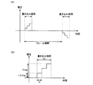
本発明の駆動方法について、図1を用いて説明する。図1(A)は、本発明において信号線に与えられる電圧のタイミングチャートを示している。図1(A)では、最初に出現している書き込み期間において、ビデオ信号の電圧が、共通の電圧から+Vsigまで階段状に段階的に推移するように信号線Siに与えられている。図1(A)において最初に出現している書き込み期間の、タイミングチャートの拡大図を図1(B)に示す。
(Embodiment 1)
The driving method of the present invention will be described with reference to FIG. FIG. 1A shows a timing chart of voltages applied to signal lines in the present invention. In FIG. 1A, the voltage of the video signal is given to the signal line Si so as to change stepwise in steps from the common voltage to + Vsig in the writing period that appears first. FIG. 1B shows an enlarged view of the timing chart in the writing period that first appears in FIG.
具体的には、図1(B)に示すように、書き込み期間が開始されると、信号線の電圧がまず+ΔVsigだけ変化する。ただし、|ΔVsig|<|Vsig|であるものとする。そして+ΔVsigだけ電圧が変化した後、時間tsが経過したら、再び信号線の電圧は+ΔVsigだけ変化する。ただし、書き込み期間の長さをtwとすると、ts<twであるものとする。 Specifically, as shown in FIG. 1B, when the writing period starts, the voltage of the signal line first changes by + ΔVsig. However, it is assumed that | ΔVsig | <| Vsig |. Then, after time ts has elapsed after the voltage has changed by + ΔVsig, the voltage of the signal line again changes by + ΔVsig. However, when the length of the writing period is tw, it is assumed that ts <tw.
そして次に時間tsが経過したら、再び信号線の電圧は+ΔVsigだけ変化する。これを順に繰り返し、最終的に信号線の電圧は+Vsigに到達する。そして次に出現する書き込み期間では、図1(A)に示すように、時間tsごとに信号線の電圧が−ΔVsigずつ変化するように駆動を行う。 Then, when the time ts elapses, the voltage of the signal line changes again by + ΔVsig. This is repeated in order, and finally the voltage of the signal line reaches + Vsig. In the next writing period, as shown in FIG. 1A, driving is performed such that the voltage of the signal line changes by −ΔVsig every time ts.
次に、本発明の効果についてよりわかりやすく説明するために、従来の場合と本発明の場合とで、ソースとドレイン間の電圧の時間変化を比較する。 Next, in order to explain the effect of the present invention more clearly, the time variation of the voltage between the source and the drain is compared between the conventional case and the case of the present invention.
まず従来のように、書き込み期間において、信号線に最初から所定の電圧を与える場合における、ソースとドレイン間の電圧Vds1について考察する。直前に信号線に与えられたビデオ信号の電圧を+Vsigとし、次の書き込み期間においてビデオ信号の電圧−Vsigが信号線に与えられるものと仮定する。このとき、画素電極では正電荷が放出され、負電荷が注入されるため、表示素子が有する画素電極の電圧をVp(t)とすると、Vp(t)は以下の式1で表される。
First, the voltage Vds1 between the source and the drain when a predetermined voltage is applied to the signal line from the beginning in the writing period as in the prior art will be considered. Assume that the voltage of the video signal applied to the signal line immediately before is + Vsig, and that the video signal voltage −Vsig is applied to the signal line in the next writing period. At this time, positive charges are emitted from the pixel electrode and negative charges are injected. Therefore, when the voltage of the pixel electrode included in the display element is Vp (t), Vp (t) is expressed by
(式1)
Vp(t)=Vsig×e−t/τ−Vsig×(1−e−t/τ)=−Vsig×(1−2e−t/τ)
(Formula 1)
Vp (t) = Vsig * e- t / τ -Vsig * (1-e- t / τ ) =-Vsig * (1-2e- t / τ )
よって、信号線に最初から所定の電圧を与える場合、ソースとドレイン間の電圧Vds1は、以下の式2で表される。
Therefore, when a predetermined voltage is applied to the signal line from the beginning, the voltage Vds1 between the source and the drain is expressed by the following
(式2)
Vds1=Vp(t)−(−Vsig)=−Vsig×(1−2e−t/τ)+Vsig=2Vsig×e−t/τ
(Formula 2)
Vds1 = Vp (t) − (− Vsig) = − Vsig × (1-2e− t / τ ) + Vsig = 2Vsig × e− t / τ
式2から、tを無限大にするとソースとドレイン間の電圧Vds1が0になるのを確かめることができる。そして式2から、従来の場合はtが0だとソースとドレイン間の電圧Vds1が2Vsigになることがわかる。
From
次に、上記特許文献1のように、信号線に与えるビデオ信号の電圧を、徐々に推移させながら最終的に所望の高さにする場合における、ソースとドレイン間の電圧Vds2について考察する。まず、直前に信号線に与えられたビデオ信号の電圧を+Vsig、書き込み時間をtwとすると、信号線の電圧Vs(t)は、以下の式3で表される。
Next, the voltage Vds2 between the source and the drain in the case where the voltage of the video signal applied to the signal line is finally set to a desired height while gradually changing as in
(式3)
Vs(t)=−(Vsig/tw)×t
(Formula 3)
Vs (t) = − (Vsig / tw) × t
表示素子で形成される容量の容量値をCl、表示素子が有する一対の電極間にかかる電圧を保持するための容量の容量値をCsとする。そして上記2つの容量に蓄積される電荷量のトータルの値をQとすると、以下の式4が成り立つ。
A capacitance value of a capacitor formed by the display element is Cl, and a capacitance value of a capacitor for holding a voltage applied between a pair of electrodes included in the display element is Cs. Then, if the total value of the amount of charge accumulated in the two capacitors is Q, the following
(式4)
Q=(Cs+Cl)×Vp(t)
(Formula 4)
Q = (Cs + Cl) × Vp (t)
さらに配線抵抗をRとすると、次の式5が成り立つ。
Further, when the wiring resistance is R, the following
(式5)
dQ/dt=(Cs+Cl)×(dVp(t)/dt)=−(Vp(t)−Vs(t))/R
(Formula 5)
dQ / dt = (Cs + Cl) × (dVp (t) / dt) = − (Vp (t) −Vs (t)) / R
次にτ=(Cs+Cl)×Rとすると、式5から式6が導き出される。
Next, assuming that τ = (Cs + Cl) × R,
(式6)
dVp(t)/dt=−(Vp(t)−Vs(t))/τ
(Formula 6)
dVp (t) / dt = − (Vp (t) −Vs (t)) / τ
ここで式1を式6に代入すると、式7が導き出される。
Here, when
(式7)
dVp(t)/dt=−(Vp(t)+(Vsig/tw)×t)/τ
(Formula 7)
dVp (t) / dt = − (Vp (t) + (Vsig / tw) × t) / τ
式7をtについて微分し、dVp(t)/dt=F(t)とおくと、式8が導き出される。 Differentiating Equation 7 with respect to t and setting dVp (t) / dt = F (t), Equation 8 is derived.
(式8)
dF(t)/dt=−(F(t)+Vsig/tw)/τ
(Formula 8)
dF (t) / dt = − (F (t) + Vsig / tw) / τ
なお、Vsig/twは定数なので、式9が成り立つ。 Since Vsig / tw is a constant, Equation 9 holds.
(式9)
dF(t)/dt=d(F(t)+Vsig/tw)/dt
(Formula 9)
dF (t) / dt = d (F (t) + Vsig / tw) / dt
式9を式8に代入すると、式10が得られる。 Substituting Equation 9 into Equation 8 yields Equation 10.
(式10)
d(F(t)+Vsig/tw)/dt=−(F(t)+Vsig/tw)/τ
(Formula 10)
d (F (t) + Vsig / tw) / dt =-(F (t) + Vsig / tw) / τ
式10は、F(t)+Vsig/twを微分すると元の関数に戻ることを示しているので、F(t)+Vsig/twが指数関数であることを意味する。よって、以下の式11が成り立つ。 Since Equation 10 indicates that when F (t) + Vsig / tw is differentiated, it returns to the original function, which means that F (t) + Vsig / tw is an exponential function. Therefore, the following expression 11 is established.
(式11)
F(t)+Vsig/tw=A×e−t/τ(Aは定数)
(Formula 11)
F (t) + Vsig / tw = A × e −t / τ (A is a constant)
dVp(t)/dt=F(t)なので、式11から以下の式12が得られる。 Since dVp (t) / dt = F (t), the following Expression 12 is obtained from Expression 11.
(式12)
dVp(t)/dt=A×e−t/τ−Vsig/tw
(Formula 12)
dVp (t) / dt = A * e- t / τ- Vsig / tw
式12を積分すると、以下の式13が導き出される。 When Equation 12 is integrated, the following Equation 13 is derived.
(式13)
Vp(t)=−τ×A×e−t/τ−(Vsig/tw)×t
(Formula 13)
Vp (t) = − τ × A × e −t / τ − (Vsig / tw) × t
なおVp(0)=Vsigとすると、式13からA=−Vsig/τであることがわかる。よって、式13にAを代入すると、以下の式14が得られる。 If Vp (0) = Vsig, it can be seen from Equation 13 that A = −Vsig / τ. Therefore, substituting A into Equation 13 yields Equation 14 below.
(式14)
Vp(t)=Vsig×e−t/τ−(Vsig/tw)×t
(Formula 14)
Vp (t) = Vsig × e −t / τ − (Vsig / tw) × t
よって、式14から、特許文献1におけるソースとドレイン間の電圧Vds2は、以下の式15で表すことができる。
Therefore, from Expression 14, the voltage Vds2 between the source and the drain in
(式15)
Vds2=Vp(t)−Vs(t)=Vsig×e−t/τ
(Formula 15)
Vds2 = Vp (t) −Vs (t) = Vsig × e− t / τ
式15から、tを無限大にするとソースとドレイン間の電圧Vds2が0になるのを確かめることができる。また式15から、tが0だとソースとドレイン間の電圧Vds2がVsigになることがわかる。 From Equation 15, it can be confirmed that the voltage Vds2 between the source and the drain becomes 0 when t is infinite. Further, it can be seen from Expression 15 that when t is 0, the voltage Vds2 between the source and the drain becomes Vsig.
次に、本発明のように、信号線に与えるビデオ信号の電圧を段階的に推移させながら、最終的に所望の高さにする場合における、ソースとドレイン間の電圧Vds3及びVds4について考察する。 Next, the voltages Vds3 and Vds4 between the source and the drain in the case where the voltage of the video signal applied to the signal line is changed to the desired height while being gradually changed as in the present invention will be considered.
本実施の形態では、直前に信号線に与えられたビデオ信号の電圧を+Vsigとする。そして、書き込み時間tw内において、数段階に分けて−ΔVsigずつ信号線に与える電圧を変化させるものとし、電圧を変化させた後、次に信号線に与える電圧を−ΔVsigだけ変化させるまでの期間をtsとする。tsは書き込み期間twより短い。 In this embodiment, the voltage of the video signal applied to the signal line immediately before is + Vsig. Then, within the write time tw, the voltage applied to the signal line is changed in several stages in several stages, and after the voltage is changed, the period until the voltage applied to the signal line is changed by -ΔVsig. Is ts. ts is shorter than the writing period tw.
まず0≦t≦tsにおける、ソースとドレイン間の電圧Vds3について考察する。0≦t≦tsの場合、Vs(t)=−ΔVsigであるので、Vs(t)は一定である。よって電圧Vds3は以下の式16で表される。 First, the voltage Vds3 between the source and the drain when 0 ≦ t ≦ ts will be considered. In the case of 0 ≦ t ≦ ts, Vs (t) = − ΔVsig, so Vs (t) is constant. Therefore, the voltage Vds3 is expressed by the following Expression 16.
(式16)
Vds3=Vp(t)−Vs(t)=Vp(t)+ΔVsig
(Formula 16)
Vds3 = Vp (t) −Vs (t) = Vp (t) + ΔVsig
また本発明では、従来と同じく式4が成り立つ。よって配線抵抗をRとすると、以下の式17が成り立つ。
In the present invention,
(式17)
dQ/dt=(Cs+Cl)×(dVp(t)/dt)=−(Vp(t)+ΔVsig)/R
(Formula 17)
dQ / dt = (Cs + Cl) × (dVp (t) / dt) = − (Vp (t) + ΔVsig) / R
次にτ=(Cs+Cl)×Rとすると、式17から式18が導き出される。 Next, when τ = (Cs + Cl) × R, Expression 18 is derived from Expression 17.
(式18)
dVp(t)/dt=−(Vp(t)+ΔVsig)/τ
(Formula 18)
dVp (t) / dt = − (Vp (t) + ΔVsig) / τ
ΔVsigは定数なので、式19が成り立つ。 Since ΔVsig is a constant, Equation 19 holds.
(式19)
dVp(t)/dt=d(Vp(t)+ΔVsig)/dt
(Formula 19)
dVp (t) / dt = d (Vp (t) + ΔVsig) / dt
式19を式18に代入すると、式20が得られる。 Substituting Equation 19 into Equation 18 yields Equation 20.
(式20)
d(Vp(t)+ΔVsig)/dt=−(Vp(t)+ΔVsig)/τ
(Formula 20)
d (Vp (t) + ΔVsig) / dt = − (Vp (t) + ΔVsig) / τ
式20は、Vp(t)+ΔVsigを微分すると元の関数に戻ることを示しているので、Vp(t)+ΔVsigが指数関数であることを意味する。よって、以下の式21が成り立つ。 Since Expression 20 indicates that when Vp (t) + ΔVsig is differentiated, it returns to the original function, which means that Vp (t) + ΔVsig is an exponential function. Therefore, the following expression 21 is established.
(式21)
Vp(t)+ΔVsig=B×e−t/τ(Bは定数)
(Formula 21)
Vp (t) + ΔVsig = B × e −t / τ (B is a constant)
なおVp(0)=Vsigとすると、式21からB=Vsig+ΔVsigであることがわかる。よって、式21にBを代入すると、以下の式22が得られる。 If Vp (0) = Vsig, it can be seen from Equation 21 that B = Vsig + ΔVsig. Thus, substituting B into Equation 21 yields Equation 22 below.
(式22)
Vp(t)=−ΔVsig+(Vsig+ΔVsig)×e−t/τ
(Formula 22)
Vp (t) = − ΔVsig + (Vsig + ΔVsig) × e −t / τ
よって、式22から、本発明の0≦t≦tsにおけるソースとドレイン間の電圧Vds3は、以下の式23で表すことができる。 Therefore, from Expression 22, the voltage Vds3 between the source and the drain in the case of 0 ≦ t ≦ ts of the present invention can be expressed by Expression 23 below.
(式23)
Vds3=Vp(t)−Vs(t)=(Vsig+ΔVsig)×e−t/τ
(Formula 23)
Vds3 = Vp (t) −Vs (t) = (Vsig + ΔVsig) × e −t / τ
式23から、tを無限大にするとソースとドレイン間の電圧Vds3が0になるのを確かめることができる。また式23から、tが0だとソースとドレイン間の電圧Vds3がVsig+ΔVsigになることがわかる。 From Equation 23, it can be confirmed that the voltage Vds3 between the source and the drain becomes 0 when t is infinite. Further, it can be seen from Expression 23 that when t is 0, the voltage Vds3 between the source and the drain becomes Vsig + ΔVsig.
次に、ts<t≦2tsにおける、ソースとドレイン間の電圧Vds4について考察する。ts<t≦2tsの場合、Vs(t)=−2ΔVsigであるので、Vs(t)は一定である。よって電圧Vds4は以下の式24で表される。 Next, the voltage Vds4 between the source and the drain when ts <t ≦ 2ts will be considered. In the case of ts <t ≦ 2ts, Vs (t) = − 2ΔVsig, so Vs (t) is constant. Therefore, the voltage Vds4 is expressed by the following Expression 24.
(式24)
Vds4=Vp(t)−Vs(t)=Vp(t)+2ΔVsig
(Formula 24)
Vds4 = Vp (t) −Vs (t) = Vp (t) + 2ΔVsig
また本発明では、従来と同じく式4が成り立つ。よって配線抵抗をRとすると、以下の式25が成り立つ。
In the present invention,
(式25)
dQ/dt=(Cs+Cl)×(dVp(t)/dt)=−(Vp(t)+2ΔVsig)/R
(Formula 25)
dQ / dt = (Cs + Cl) × (dVp (t) / dt) = − (Vp (t) + 2ΔVsig) / R
次にτ=(Cs+Cl)×Rとすると、式25から式26が導き出される。 Next, when τ = (Cs + Cl) × R, Expression 26 is derived from Expression 25.
(式26)
dVp(t)/dt=−(Vp(t)+2ΔVsig)/τ
(Formula 26)
dVp (t) / dt = − (Vp (t) + 2ΔVsig) / τ
2ΔVsigは定数なので、式27が成り立つ。 Since 2ΔVsig is a constant, Equation 27 holds.
(式27)
dVp(t)/dt=d(Vp(t)+2ΔVsig)/dt
(Formula 27)
dVp (t) / dt = d (Vp (t) + 2ΔVsig) / dt
式27を式26に代入すると、式28が得られる。 Substituting Equation 27 into Equation 26 yields Equation 28.
(式28)
d(Vp(t)+2ΔVsig)/dt=−(Vp(t)+2ΔVsig)/τ
(Formula 28)
d (Vp (t) + 2ΔVsig) / dt = − (Vp (t) + 2ΔVsig) / τ
式28は、Vp(t)+2ΔVsigを微分すると元の関数に戻ることを示しているので、Vp(t)+2ΔVsigが指数関数であることを意味する。よって、以下の式29が成り立つ。 Since Equation 28 indicates that when Vp (t) + 2ΔVsig is differentiated, it returns to the original function, which means that Vp (t) + 2ΔVsig is an exponential function. Therefore, the following expression 29 is established.
(式29)
Vp(t)+2ΔVsig=C×e−t/τ(Cは定数)
(Formula 29)
Vp (t) + 2ΔVsig = C × e −t / τ (C is a constant)
なおVp(0)=−ΔVsigとすると、式29からB=ΔVsigであることがわかる。よって、式29にCを代入し、最後にtをt−tsに置き換えると、以下の式30が得られる。 If Vp (0) = − ΔVsig, it can be seen from Equation 29 that B = ΔVsig. Therefore, substituting C into Equation 29 and finally replacing t with t-ts yields Equation 30 below.
(式30)
Vp(t)=−2ΔVsig+Vsig×e−(t−ts)/τ
(Formula 30)
Vp (t) = − 2ΔVsig + Vsig × e− (t−ts) / τ
よって、式30から、本発明のts<t≦2tsにおけるソースとドレイン間の電圧Vds4は、最後にtをt−tsに置き換えると、以下の式31で表すことができる。 Therefore, from Expression 30, the voltage Vds4 between the source and the drain at ts <t ≦ 2ts of the present invention can be expressed by the following Expression 31 when t is finally replaced with t−ts.
(式31)
Vds4=Vp(t)−Vs(t)=ΔVsig×e−(t−ts)/τ
(Formula 31)
Vds4 = Vp (t) −Vs (t) = ΔVsig × e− (t−ts) / τ
式31から、本発明のts<t≦2tsにおけるソースとドレイン間の電圧Vds4の最大値がΔVsigであることがわかる。そして、tの範囲をm×ts<t≦(m+1)×ts<tw(ただし、mは1より大きい整数)と一般化した場合においても、ソースとドレイン間の電圧は式31で表される。よってtの範囲がm×ts<t≦(m+1)×ts<twの場合、ソースとドレイン間の電圧の最大値はΔVsigとなる。 From Expression 31, it can be seen that the maximum value of the voltage Vds4 between the source and the drain at ts <t ≦ 2ts of the present invention is ΔVsig. Even when the range of t is generalized as m × ts <t ≦ (m + 1) × ts <tw (where m is an integer greater than 1), the voltage between the source and the drain is expressed by Equation 31. . Therefore, when the range of t is m × ts <t ≦ (m + 1) × ts <tw, the maximum value of the voltage between the source and the drain is ΔVsig.
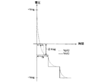
図2に、本発明における画素電極の電圧Vp(t)と、信号線の電圧Vs(t)の時間変化を示す。図2に示すように、電荷の緩和時間τよりも大きくなるように時間tsの値を設定した場合、時間tsごとに信号線の電圧Vs(t)が変化すると、それに追随するように電圧Vp(t)の値も変化するのが分かる。 FIG. 2 shows temporal changes of the pixel electrode voltage Vp (t) and the signal line voltage Vs (t) in the present invention. As shown in FIG. 2, when the value of the time ts is set so as to be longer than the charge relaxation time τ, the voltage Vp follows the voltage Vs (t) of the signal line that changes at each time ts. It can be seen that the value of (t) also changes.
次に、従来の、信号線に最初から所定の電圧を与える場合における、ソースとドレイン間の電圧Vds1と、特許文献1の、信号線に与えるビデオ信号の電圧を、徐々に推移させながら最終的に所望の高さにする場合における、ソースとドレイン間の電圧Vds2と、本発明の、信号線に与えるビデオ信号の電圧を段階的に推移させながら最終的に所望の高さにする場合における、ソースとドレイン間の電圧Vds3及びVds4の、時間変化を比較する。
Next, in the case of applying a predetermined voltage from the beginning to the conventional signal line, the voltage Vds1 between the source and the drain and the voltage of the video signal applied to the signal line of
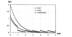
なお本実施の形態では、比較を平易に行うことができるように、Vsig=1、τ=1、tw/τ=6、ΔVsig=1/6、ts=1と仮定する。そして上記仮定のもと、式2、式15、式24、式31を用いることで得られるソースとドレイン間の電圧の時間変化を、図3に示す。
In this embodiment, it is assumed that Vsig = 1, τ = 1, tw / τ = 6, ΔVsig = 1/6, and ts = 1 so that the comparison can be easily performed. FIG. 3 shows the time change of the voltage between the source and the drain obtained by using
図3から分かるように、本発明の場合、書き込み期間において最初に電圧を−ΔVsigだけ変化させた際に、電圧Vds2よりもΔVsigだけ、ソースとドレイン間の電圧の絶対値が大きくなっているが、その後の期間においてはソースとドレイン間の電圧の絶対値はVds1とVds2に比べてその最大値を小さく抑えることができる。 As can be seen from FIG. 3, in the case of the present invention, when the voltage is first changed by −ΔVsig in the writing period, the absolute value of the voltage between the source and the drain is larger by ΔVsig than by the voltage Vds2. In the subsequent period, the absolute value of the voltage between the source and the drain can be suppressed to be smaller than that of Vds1 and Vds2.
従って本発明では、書き込み期間において、スイッチング素子として用いるトランジスタのソースとドレイン間の電圧の絶対値を従来よりも小さくすることができるので、該トランジスタのドレイン近傍に高電界が発生するのを抑えることができる。そして本発明の構成により、スイッチング素子の信頼性の向上、延いては表示装置の信頼性の向上を実現することができる。 Therefore, in the present invention, the absolute value of the voltage between the source and the drain of the transistor used as the switching element can be made smaller than before in the writing period, so that generation of a high electric field in the vicinity of the drain of the transistor is suppressed. Can do. With the configuration of the present invention, it is possible to improve the reliability of the switching element, and thus improve the reliability of the display device.
なお図1では、信号線の電圧が3段階に渡って変化している場合を例示しているが、本発明はこの構成に限定されない。信号線の電圧が2段階で変化していても良いし、4段階以上で変化していても良い。 Note that FIG. 1 illustrates the case where the voltage of the signal line changes in three stages, but the present invention is not limited to this configuration. The voltage of the signal line may change in two stages, or may change in four or more stages.
また各段階における電圧の変化量は、必ずしも一定である必要はない。段階ごとに電圧の変化量にも差を設けるようにしても良い。例えば前の書き込み期間において極性が異なる電圧が印加されている場合、書き込み期間の一段階目に変化させる電圧の変化量を、他の段階における変化量よりも小さく抑えることで、スイッチング素子として用いるトランジスタの、一段階目におけるソースとドレイン間の電圧をより小さく抑えることができる。特に一段階目で基準となる電圧を与え、次の段階から信号線に与える電圧を変化させるようにすることで、書き込み期間の一段階目におけるソースとドレイン間の電圧を、特許文献1の場合のソースとドレイン間の電圧と同様に、小さく抑えることができる。
Further, the amount of change in voltage at each stage is not necessarily constant. You may make it provide a difference also in the variation | change_quantity of a voltage for every step. For example, when voltages having different polarities are applied in the previous writing period, the amount of change in voltage that is changed in the first stage of the writing period is suppressed to be smaller than that in other stages, so that the transistor used as a switching element Thus, the voltage between the source and drain in the first stage can be further reduced. In particular, by applying a reference voltage in the first stage and changing the voltage applied to the signal line from the next stage, the voltage between the source and the drain in the first stage of the writing period is the same as in the case of
なお本発明で行われる交流駆動は、任意の1フレーム期間において全ての画素に同じ極性を有するビデオ信号が入力されるフレーム反転駆動の他、ソースライン反転駆動、ゲートライン反転駆動、ドット反転駆動またはその他の反転駆動であっても良い。ソースライン反転駆動とは、任意の1フレーム期間において、一の信号線に接続されている全ての画素に同じ極性のビデオ信号が入力され、隣り合う信号線に接続されている画素どうしで逆の極性のビデオ信号が入力される駆動方法である。ゲートライン反転駆動とは、任意の1フレーム期間において、一の走査線に接続されている全ての画素に同じ極性のビデオ信号が入力され、隣り合う走査線に接続されている画素どうしで逆の極性のビデオ信号が入力される駆動方法である。ドット反転駆動とは、任意の1フレーム期間において、隣接する画素どうしで逆の極性のビデオ信号が入力される駆動方法である。 The AC driving performed in the present invention includes source inversion driving, gate line inversion driving, dot inversion driving, or frame inversion driving in which a video signal having the same polarity is input to all pixels in an arbitrary frame period. Other inversion driving may be used. Source line inversion driving is the reverse of video signals having the same polarity input to all pixels connected to one signal line in any one frame period and between pixels connected to adjacent signal lines. This is a driving method in which a polar video signal is input. Gate line inversion driving is the reverse of video signals having the same polarity input to all pixels connected to one scanning line in any one frame period, and the pixels connected to adjacent scanning lines are reversed. This is a driving method in which a polar video signal is input. The dot inversion driving is a driving method in which video signals having opposite polarities are input between adjacent pixels in any one frame period.
(実施の形態2)
実施の形態1とは異なる駆動方法について、図4を用いて説明する。図4(A)は、本発明において信号線に与えられる電圧のタイミングチャートを示している。図4(A)では、実施の形態1と同様に、最初に出現する書き込み期間において、信号線Siにビデオ信号の電圧+Vsigが段階的に与えられている。図4(A)において最初に出現している書き込み期間の、タイミングチャートの拡大図を図4(B)に示す。
(Embodiment 2)
A driving method different from that of
図4(B)に示すように、書き込み期間が開始されると、信号線の電圧がまず+ΔVsigだけ変化する。ただし、|ΔVsig|<|Vsig|であるものとする。そして本実施の形態では、前出の容量CsとClの電荷量の変化が信号線の電圧の変化により追随しやすいように、信号線の電圧を変化させる。具体的には、実施の形態1では、その波形が矩形となるように+ΔVsig分の電圧を上げるが、本実施の形態では+ΔVsig分の電圧の立ち上がりを遅らせて、その波形に放物形状の鈍りが生じるようにする。 As shown in FIG. 4B, when the writing period starts, the voltage of the signal line first changes by + ΔVsig. However, it is assumed that | ΔVsig | <| Vsig |. In this embodiment, the voltage of the signal line is changed so that the change in the charge amount of the capacitors Cs and Cl can easily follow the change in the voltage of the signal line. Specifically, in the first embodiment, the voltage is increased by + ΔVsig so that the waveform is rectangular, but in this embodiment, the rise of the voltage by + ΔVsig is delayed and the waveform has a dull parabolic shape. To occur.
次に+ΔVsigだけ電圧が変化した後、時間tsが経過したら、再び信号線の電圧は+ΔVsigだけ変化する。ただし、書き込み期間の長さをtwとすると、ts<twであるものとする。そして次に時間tsが経過した後に、再び信号線の電圧は+ΔVsigだけ同様に変化する。これを順に繰り返し、最終的に信号線の電圧は+Vsigに到達する。なお、2段階目以降の電圧の変化も、1段階目と同様に、+ΔVsig分の電圧の立ち上がりを遅らせてその波形に鈍りが生じるようにする。 Next, after the voltage changes by + ΔVsig, when the time ts elapses, the voltage of the signal line changes again by + ΔVsig. However, when the length of the writing period is tw, it is assumed that ts <tw. Then, after the time ts has passed, the voltage of the signal line again changes similarly by + ΔVsig. This is repeated in order, and finally the voltage of the signal line reaches + Vsig. As for the voltage change after the second stage, the rise of the voltage by + ΔVsig is delayed so that the waveform becomes dull, as in the first stage.
そして次に出現する書き込み期間では、図4(A)に示すように、時間tsごとに信号線の電圧が−ΔVsigずつ変化するように駆動を行う。電圧が−ΔVsigずつ変化する場合も、+ΔVsigずつ変化する場合と同様に、前出の容量CsとClの電荷量の変化が信号線の電圧の変化により追随しやすいように、信号線の電圧を変化させる。具体的には、本来ならば、その波形が矩形となるように−ΔVsig分の電圧を下げるところを、−ΔVsig分の電圧の立ち上がりを遅らせて、その波形に鈍りが生じるようにする。 Then, in the next writing period, as shown in FIG. 4A, driving is performed so that the voltage of the signal line changes by −ΔVsig every time ts. When the voltage changes by -ΔVsig, the voltage of the signal line is set so that the change in the charge amount of the capacitances Cs and Cl easily follows the change of the voltage of the signal line, as in the case of changing by + ΔVsig. Change. Specifically, if the voltage is lowered by −ΔVsig so that the waveform is rectangular, the rise of the voltage by −ΔVsig is delayed so that the waveform becomes dull.
次に、本実施の形態のように、信号線に与えるビデオ信号の電圧を段階的に推移させながら、最終的に所望の高さにする場合における、ソースとドレイン間の電圧Vds5及びVds6について考察する。 Next, as in this embodiment, the voltages Vds5 and Vds6 between the source and the drain when the voltage of the video signal applied to the signal line is changed to a desired level while being gradually changed are considered. To do.
本実施の形態では、直前に信号線に与えられたビデオ信号の電圧を+Vsigとする。また信号線に与える電圧の波形を、電荷の蓄積時間τ=(Cs+Cl)×Rだけ遅延させる場合について考察する。なお、書き込み時間tw内において、数段階に分けて−ΔVsigずつ信号線に与える電圧を変化させるものとし、信号線に与える電圧を−ΔVsigだけ変化させるまでの期間をtsとする。tsは書き込み期間twより短い。 In this embodiment, the voltage of the video signal applied to the signal line immediately before is + Vsig. Consider a case where the waveform of the voltage applied to the signal line is delayed by the charge accumulation time τ = (Cs + Cl) × R. Note that the voltage applied to the signal line is changed by −ΔVsig in several steps within the write time tw, and the period until the voltage applied to the signal line is changed by −ΔVsig is denoted by ts. ts is shorter than the writing period tw.
まず0≦t≦tsにおける、ソースとドレイン間の電圧Vds5について考察する。0≦t≦tsの場合、Vs(t)=−ΔVsig×(1−e−t/τ)である。よって電圧Vds5は以下の式32で表される。 First, the voltage Vds5 between the source and the drain when 0 ≦ t ≦ ts will be considered. In the case of 0 ≦ t ≦ ts, Vs (t) = − ΔVsig × (1−e− t / τ ). Therefore, the voltage Vds5 is expressed by the following equation 32.
(式32)
Vds5=Vp(t)−Vs(t)=Vp(t)+ΔVsig×(1−e−t/τ)
(Formula 32)
Vds5 = Vp (t) −Vs (t) = Vp (t) + ΔVsig × (1−e− t / τ )
また本発明では、従来と同じく式4が成り立つ。よって配線抵抗をRとすると、以下の式33が成り立つ。
In the present invention,
(式33)
dQ/dt=(Cs+Cl)×(dVp(t)/dt)=−(Vp(t)+ΔVsig×(1−e−t/τ))/R
(Formula 33)
dQ / dt = (Cs + Cl) × (dVp (t) / dt) = − (Vp (t) + ΔVsig × (1−e− t / τ )) / R
次にτ=(Cs+Cl)×Rとすると、式33から式34が導き出される。 Next, when τ = (Cs + Cl) × R, Expression 34 is derived from Expression 33.
(式34)
dVp(t)/dt=−(Vp(t)+ΔVsig×(1−e−t/τ))/τ
(Formula 34)
dVp (t) / dt = − (Vp (t) + ΔVsig × (1−e− t / τ )) / τ
ここで、微分方程式dy/db=−a×y+Q(b)の一般解がy=e−ab×{∫eab×Q(b)db+D}(Dは定数)であることを使い、式34を解くと、式35が得られる。 Here, using the fact that the general solution of the differential equation dy / db = −a × y + Q (b) is y = e −ab × {∫e ab × Q (b) db + D} (D is a constant), Equation 34 Is solved, Equation 35 is obtained.
(式35)
Vp(t)=−ΔVsig+(t−D)×(ΔVsig/τ)×e−t/τ
(Formula 35)
Vp (t) = − ΔVsig + (t−D) × (ΔVsig / τ) × e −t / τ
初期条件としてVp(0)=+Vsigとすると、式35からD=−(τ/ΔVsig)×(ΔVsig+Vsig)であることがわかる。Dを式35に代入すると、以下の式36が得られる。 Assuming that Vp (0) = + Vsig as an initial condition, it can be seen from Equation 35 that D = − (τ / ΔVsig) × (ΔVsig + Vsig). Substituting D into Equation 35 yields Equation 36 below.
(式36)
Vp(t)=−ΔVsig+(t+(τ/ΔVsig)×(ΔVsig+Vsig))×(ΔVsig/τ)×e−t/τ
(Formula 36)
Vp (t) = − ΔVsig + (t + (τ / ΔVsig) × (ΔVsig + Vsig)) × (ΔVsig / τ) × e −t / τ
したがって、式32と式36から、Vds5は以下の式37で表される。 Therefore, from the equations 32 and 36, Vds5 is expressed by the following equation 37.
(式37)
Vds5=Vp(t)+ΔVsig×(1−e−t/τ)=(t+(τ/ΔVsig)×Vsig)×(ΔVsig/τ)×e−t/τ
(Formula 37)
Vds5 = Vp (t) + ΔVsig × (1−e− t / τ ) = (t + (τ / ΔVsig) × Vsig) × (ΔVsig / τ) × e− t / τ
次に、ts<t≦2tsにおける、ソースとドレイン間の電圧Vds6について考察する。ts<t≦2tsの場合、Vs(t)=−ΔVsig×(1−e−t/τ)−ΔVsig=−ΔVsig×(2−e−t/τ)である。よって電圧Vds6は以下の式38で表される。 Next, the voltage Vds6 between the source and the drain when ts <t ≦ 2ts will be considered. When ts <t ≦ 2ts, Vs (t) = − ΔVsig × (1−e− t / τ ) −ΔVsig = −ΔVsig × (2−e− t / τ ). Therefore, the voltage Vds6 is expressed by the following formula 38.
(式38)
Vds6=Vp(t)−Vs(t)=Vp(t)+ΔVsig×(2−e−t/τ)
(Formula 38)
Vds6 = Vp (t) −Vs (t) = Vp (t) + ΔVsig × (2-e− t / τ )
また本発明では、従来と同じく式4が成り立つ。よって配線抵抗をRとすると、以下の式39が成り立つ。
In the present invention,
(式39)
dQ/dt=(Cs+Cl)×(dVp(t)/dt)=−(Vp(t)+ΔVsig×(2−e−t/τ))/R
(Formula 39)
dQ / dt = (Cs + Cl) × (dVp (t) / dt) = − (Vp (t) + ΔVsig × (2-e− t / τ )) / R
次にτ=(Cs+Cl)×Rとすると、式39から式40が導き出される。 Next, assuming that τ = (Cs + Cl) × R, Expression 40 is derived from Expression 39.
(式40)
dVp(t)/dt=−(Vp(t)+ΔVsig×(2−e−t/τ))/τ
(Formula 40)
dVp (t) / dt = − (Vp (t) + ΔVsig × (2-e− t / τ )) / τ
ここで、dy/db=−a×y+Q(b)の解がy=e−ab×{∫eab×Q(b)db+E}(Eは定数)であることを使い、式40を解くと、式41が得られる。 Here, using the fact that the solution of dy / db = −a × y + Q (b) is y = e −ab × {∫e ab × Q (b) db + E} (E is a constant), Equation 41 is obtained.
(式41)
Vp(t)=−(ΔVsig/τ)×e−t/τ{2τ×e(t/τ)−t+E}
(Formula 41)
Vp (t) = − (ΔVsig / τ) × e −t / τ {2τ × e (t / τ) −t + E}
初期条件としてVp(0)=−ΔVsigとすると、式41からE=−τであることがわかる。Eを式41に代入し、最後にtをt―tsに置き換えると、以下の式42が得られる。 Assuming that Vp (0) = − ΔVsig as an initial condition, E = −τ is found from Equation 41. Substituting E into equation 41 and finally substituting t with ts, the following equation 42 is obtained.
(式42)
Vp(t)=−(ΔVsig/τ)×e−(t−ts)/τ{2τ×e((t−ts)/τ)−(t−ts)−τ}
(Formula 42)
Vp (t) = − (ΔVsig / τ) × e − (t−ts) / τ {2τ × e ((t−ts) / τ) − (t−ts) −τ}
したがって、式38と式42から、tをt―tsに置き換えると、Vds6は以下の式43で表される。 Therefore, when t is replaced with t−ts from the equations 38 and 42, Vds6 is expressed by the following equation 43.
(式43)
Vds6=Vp(t)+ΔVsig×(2−e−(t−ts)/τ)=((t−ts)/τ)×ΔVsig×e−(t−ts)/τ
(Formula 43)
Vds6 = Vp (t) + ΔVsig × (2-e− (t−ts) / τ ) = ((t−ts) / τ) × ΔVsig × e− (t−ts) / τ
なお、tの範囲をm×ts<t≦(m+1)×ts<tw(ただし、mは1より大きい整数)と一般化した場合においても、ソースとドレイン間の電圧は式43で表される。 Even when the range of t is generalized as m × ts <t ≦ (m + 1) × ts <tw (where m is an integer greater than 1), the voltage between the source and the drain is expressed by Equation 43. .
図5に、本実施の形態における画素電極の電圧Vp(t)と、信号線の電圧Vs(t)の時間依存性を示す。図5に示すように、信号線に与える電圧の波形を、蓄積時間τ=(Cs+Cl)×Rだけ遅延させる場合、時間tsごとに信号線の電圧Vs(t)が変化すると、実施の形態1の場合よりもそれに追随するように電圧Vp(t)の値も変化するのが分かる。 FIG. 5 shows the time dependency of the voltage Vp (t) of the pixel electrode and the voltage Vs (t) of the signal line in this embodiment. As shown in FIG. 5, when the voltage waveform applied to the signal line is delayed by the accumulation time τ = (Cs + Cl) × R, the voltage Vs (t) of the signal line changes every time ts. It can be seen that the value of the voltage Vp (t) also changes so as to follow the case.
次に、従来の、信号線に最初から所定の電圧を与える場合における、ソースとドレイン間の電圧Vds1と、特許文献1の、信号線に与えるビデオ信号の電圧を、徐々に推移させながら最終的に所望の高さにする場合における、ソースとドレイン間の電圧Vds2と、本発明の、信号線に与えるビデオ信号の電圧を段階的に推移させながら最終的に所望の高さにする場合における、ソースとドレイン間の電圧Vds5及びVds6の、時間依存性を比較する。
Next, in the case of applying a predetermined voltage from the beginning to the conventional signal line, the voltage Vds1 between the source and the drain and the voltage of the video signal applied to the signal line of
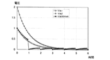
なお本実施の形態では、比較を平易に行うことができるように、Vsig=1、τ=1、tw/τ=6、ΔVsig=1/6、ts=1と仮定する。そして上記仮定のもと、式2、式15、式37、式43を用いることで得られるソースとドレイン間の電圧の時間依存性を、図6に示す。
In this embodiment, it is assumed that Vsig = 1, τ = 1, tw / τ = 6, ΔVsig = 1/6, and ts = 1 so that the comparison can be easily performed. FIG. 6 shows the time dependency of the voltage between the source and the drain obtained by using
図6から分かるように、本実施の形態によるVds5とVds6の場合、書き込み期間において最初に電圧を−ΔVsigだけ変化させた際に、Vds5とVds6の絶対値はほぼVds1とVds2と同じであるが、その後の期間においてはVds5とVds6の絶対値はVds1とVds2に比べてその最大値を小さく抑えることができる。 As can be seen from FIG. 6, in the case of Vds5 and Vds6 according to the present embodiment, when the voltage is first changed by −ΔVsig in the writing period, the absolute values of Vds5 and Vds6 are substantially the same as Vds1 and Vds2. In the subsequent period, the absolute values of Vds5 and Vds6 can be kept smaller than those of Vds1 and Vds2.
なお図4では、信号線の電圧が3段階に渡って変化している場合を例示しているが、本発明はこの構成に限定されない。信号線の電圧が2段階で変化していても良いし、4段階以上で変化していても良い。 Note that FIG. 4 illustrates the case where the voltage of the signal line changes in three stages, but the present invention is not limited to this configuration. The voltage of the signal line may change in two stages, or may change in four or more stages.
また各段階における電圧の変化量は、必ずしも一定である必要はない。段階ごとに電圧の変化量にも差を設けるようにしても良い。例えば前の書き込み期間において極性が異なる電圧が印加されている場合、書き込み期間の一段階目に変化させる電圧の変化量を、他の段階における変化量よりも小さく抑えることで、スイッチング素子として用いるトランジスタの、一段階目におけるソースとドレイン間の電圧をより小さく抑えることができる。特に一段階目で基準となる電圧を与え、次の段階から信号線に与える電圧を変化させるようにすることで、書き込み期間の一段階目におけるソースとドレイン間の電圧を、特許文献1の場合のソースとドレイン間の電圧よりも、小さく抑えることができる。
Further, the amount of change in voltage at each stage is not necessarily constant. You may make it provide a difference also in the variation | change_quantity of a voltage for every step. For example, when voltages having different polarities are applied in the previous writing period, the amount of change in voltage that is changed in the first stage of the writing period is suppressed to be smaller than that in other stages, so that the transistor used as a switching element Thus, the voltage between the source and drain in the first stage can be further reduced. In particular, by applying a reference voltage in the first stage and changing the voltage applied to the signal line from the next stage, the voltage between the source and the drain in the first stage of the writing period is the same as in the case of
従って本発明では、書き込み期間において、スイッチング素子として用いるトランジスタのソースとドレイン間の電圧の絶対値を従来よりも小さくすることができるので、該トランジスタのドレイン近傍に高電界が発生するのを抑えることができる。そして本発明の構成により、スイッチング素子の信頼性の向上、延いては表示装置の信頼性の向上を実現することができる。 Therefore, in the present invention, the absolute value of the voltage between the source and the drain of the transistor used as the switching element can be made smaller than before in the writing period, so that generation of a high electric field in the vicinity of the drain of the transistor is suppressed. Can do. With the configuration of the present invention, it is possible to improve the reliability of the switching element, and thus improve the reliability of the display device.
なお本発明で行われる交流駆動は、任意の1フレーム期間において全ての画素に同じ極性を有するビデオ信号が入力されるフレーム反転駆動の他、ソースライン反転駆動、ゲートライン反転駆動、ドット反転駆動またはその他の反転駆動であっても良い。ソースライン反転駆動とは、任意の1フレーム期間において、一の信号線に接続されている全ての画素に同じ極性のビデオ信号が入力され、隣り合う信号線に接続されている画素どうしで逆の極性のビデオ信号が入力される駆動方法である。ゲートライン反転駆動とは、任意の1フレーム期間において、一の走査線に接続されている全ての画素に同じ極性のビデオ信号が入力され、隣り合う走査線に接続されている画素どうしで逆の極性のビデオ信号が入力される駆動方法である。ドット反転駆動とは、任意の1フレーム期間において、隣接する画素どうしで逆の極性のビデオ信号が入力される駆動方法である。 The AC driving performed in the present invention includes source inversion driving, gate line inversion driving, dot inversion driving, or frame inversion driving in which a video signal having the same polarity is input to all pixels in an arbitrary frame period. Other inversion driving may be used. Source line inversion driving is the reverse of video signals having the same polarity input to all pixels connected to one signal line in any one frame period and between pixels connected to adjacent signal lines. This is a driving method in which a polar video signal is input. Gate line inversion driving is the reverse of video signals having the same polarity input to all pixels connected to one scanning line in any one frame period, and the pixels connected to adjacent scanning lines are reversed. This is a driving method in which a polar video signal is input. The dot inversion driving is a driving method in which video signals having opposite polarities are input between adjacent pixels in any one frame period.
(実施の形態3)
本実施の形態では、具体的な電荷蓄積の緩和時間の算出方法について説明する。
(Embodiment 3)
In this embodiment mode, a specific method for calculating the relaxation time of charge accumulation will be described.
画素内において配線抵抗が無視できるぐらい小さく、画素内の抵抗Rはスイッチング素子として用いられるトランジスタによるものと仮定した場合の、緩和時間τを算出する。スイッチング用のトランジスタは線形領域で動作するため、トランジスタのチャネル形成領域における抵抗は以下の式44で与えられる。なお式44において、VgsとVthはそれぞれトランジスタに印加されるゲートとソース間の電圧(ゲート電圧)と、閾値電圧とを表している。また、LとWはチャネル長とチャネル幅を表す。μは移動度、Coxはトランジスタの単位面積当たりのゲート容量を表す。 The relaxation time τ is calculated when it is assumed that the wiring resistance in the pixel is negligibly small and the resistance R in the pixel is due to a transistor used as a switching element. Since the switching transistor operates in the linear region, the resistance in the channel formation region of the transistor is given by the following Expression 44. In Equation 44, Vgs and Vth represent a gate-source voltage (gate voltage) applied to the transistor and a threshold voltage, respectively. L and W represent channel length and channel width. μ represents mobility, and C ox represents gate capacitance per unit area of the transistor.
(式44)
R=1/β(Vgs−Vth) ただしβ=(L/W)×μ×Cox
(Formula 44)
R = 1 / β (Vgs−Vth) where β = (L / W) × μ × C ox
次に、画素内における容量が液晶容量に相当すると仮定すると、画素の容量値Cpは以下の式45で表される。なお式45において、ε0とεLiqはそれぞれ真空の誘電率と液晶の比誘電率を表している。また、tLiqは液晶の膜厚を、Sは画素電極の面積を表している。 Next, assuming that the capacitance in the pixel corresponds to the liquid crystal capacitance, the capacitance value Cp of the pixel is expressed by the following Expression 45. In Equation 45, ε 0 and ε Liq represent the dielectric constant of vacuum and the relative dielectric constant of liquid crystal, respectively. T Liq represents the film thickness of the liquid crystal, and S represents the area of the pixel electrode.
(式45)
Cp=(ε0×εLiq/tLiq)×S
(Formula 45)
Cp = (ε 0 × ε Liq / t Liq ) × S
次に、アモルファスシリコンを用いたトランジスタをスイッチング素子とする液晶パネルを例に挙げ、そのL/W、μ、Cox、Vgs、Vth、εLiq、tLiq、S、Rの一般的な値を設定し、緩和時間τを算出する。具体的には、L/W=10/10μm、μ=0.5cm2/Vsec、Cox=1.8x10−4F(ゲート絶縁膜が、膜厚300nm相当の窒化珪素膜であることを想定している)、Vgs=10V、Vth=5V、εLiq=8、tLiq=6μm、S=150x150μmとする。 Next, a liquid crystal panel using a transistor using amorphous silicon as a switching element is taken as an example, and general values of L / W, μ, C ox , Vgs, Vth, ε Liq , t Liq , S, R are given as follows. Set and calculate relaxation time τ. Specifically, L / W = 10/10 μm, μ = 0.5 cm 2 / Vsec, C ox = 1.8 × 10 −4 F (assuming that the gate insulating film is a silicon nitride film equivalent to a film thickness of 300 nm. Vgs = 10 V, Vth = 5 V, ε Liq = 8, t Liq = 6 μm, and S = 150 × 150 μm.
よって、緩和時間τ=Cp×R=2.6x10−13x 2.2x107sec=5.7x10⁻⁶secとなる。VGA(480x640画素)を想定し、1フレーム期間を1/60secとすれば、1水平期間(1行書き込むのに必要な時間)は1/60/480=3.5X10−5secとなり、この1水平期間が書き込み時間twの取りうる最大値となる。信号線の電圧に相当する電荷が容量に蓄えられるためにはts>τである必要があり、おおよその可能な書き込み時間のステップの分割数はtw/τで与えられる。上の例ではtw=3.5X10−5secとして、ステップ分割数=tw/τ=3.5X10−5/(5.7x10−6)≒6となる。従って信号線の電圧を5Vとすればステップ電圧ΔVsigは5/6=0.83Vとなる。 Therefore, the relaxation time τ = Cp × R = 2.6 × 10 −13 x 2.2 × 10 7 sec = 5.7 × 10 −6 sec. If VGA (480 × 640 pixels) is assumed and one frame period is 1/60 sec, one horizontal period (time required to write one row) is 1/60/480 = 3.5 × 10 −5 sec. The horizontal period is the maximum value that the writing time tw can take. In order for the electric charge corresponding to the voltage of the signal line to be stored in the capacitor, it is necessary that ts> τ, and the approximate number of divisions of possible write time steps is given by tw / τ. In the above example, tw = 3.5 × 10 −5 sec, and the number of step divisions = tw / τ = 3.5 × 10 −5 /(5.7×10 −6 ) ≈6. Therefore, if the voltage of the signal line is 5V, the step voltage ΔVsig is 5/6 = 0.83V.
(実施の形態4)
本実施の形態では、本発明の表示装置の構成について説明する。図7(A)は、本実施の形態の表示装置のブロック図である。図7(A)に示す表示装置は、表示素子を備えた画素を複数有する画素部100と、各画素をラインごとに選択する走査線駆動回路110と、選択されたラインの画素へのビデオ信号の入力を制御する信号線駆動回路120とを有する。
(Embodiment 4)
In this embodiment mode, a structure of a display device of the present invention will be described. FIG. 7A is a block diagram of a display device of this embodiment mode. A display device illustrated in FIG. 7A includes a pixel portion 100 including a plurality of pixels each including a display element, a scanning
図7(A)において信号線駆動回路120は、シフトレジスタ121、第1のラッチ122、第2のラッチ123、レベルシフタ124を有している。シフトレジスタ121には、クロック信号S−CLK、スタートパルス信号S−SP、走査方向切替信号L/Rが入力されている。シフトレジスタ121は、これらクロック信号S−CLK及びスタートパルス信号S−SPに従って、パルスが順次シフトするタイミング信号を生成し、第1のラッチ122に出力する。タイミング信号のパルスの出現する順序は、走査方向切替信号L/Rによって切り替わる。 In FIG. 7A, the signal line driver circuit 120 includes a shift register 121, a first latch 122, a second latch 123, and a level shifter 124. The shift register 121 receives a clock signal S-CLK, a start pulse signal S-SP, and a scanning direction switching signal L / R. The shift register 121 generates a timing signal for sequentially shifting the pulses in accordance with the clock signal S-CLK and the start pulse signal S-SP, and outputs the timing signal to the first latch 122. The order in which the pulses of the timing signal appear is switched by the scanning direction switching signal L / R.
第1のラッチ122にタイミング信号が入力されると、該タイミング信号のパルスに従って、第1のラッチ122が有する複数の記憶素子にビデオ信号が順に書き込まれ、保持される。なお、信号線の数をxとし、信号線に与える電圧をm段階で変化させると仮定すると、第1のラッチ122が有する記憶素子の数は、少なくともx×m個となる。そして同一の信号線に対応するm個の記憶素子には、同じ画像情報を有するビデオ信号が入力される。 When a timing signal is input to the first latch 122, video signals are sequentially written and held in the plurality of memory elements included in the first latch 122 in accordance with the pulse of the timing signal. Note that assuming that the number of signal lines is x and the voltage applied to the signal lines is changed in m stages, the number of memory elements included in the first latch 122 is at least x × m. A video signal having the same image information is input to m memory elements corresponding to the same signal line.
なお、本実施の形態では第1のラッチ122が有する複数の記憶素子に順にビデオ信号を書き込んでいるが、本発明はこの構成に限定されない。第1のラッチ122が有する複数の記憶素子をいくつかのグループに分け、該グループごとに並行してビデオ信号を入力する、いわゆる分割駆動を行っても良い。なおこのときのグループ数を分割数と呼ぶ。例えば4つの記憶素子ごとにラッチをグループに分けた場合、4分割で分割駆動することになる。 Note that although video signals are sequentially written in the plurality of memory elements included in the first latch 122 in this embodiment, the present invention is not limited to this structure. A plurality of storage elements included in the first latch 122 may be divided into several groups, and so-called divided driving may be performed in which video signals are input in parallel for each group. Note that the number of groups at this time is called the number of divisions. For example, when the latches are divided into groups for every four storage elements, they are divided and driven in four divisions.
第1のラッチ122の全ての記憶素子への、ビデオ信号の書き込みが一通り終了するまでの時間が、水平期間(ライン期間)に相当する。実際には、上記水平期間に水平帰線期間が加えられた期間を水平期間に含むことがある。 The time until video signal writing to all the storage elements of the first latch 122 is completed corresponds to a horizontal period (line period). Actually, the horizontal period may include a period obtained by adding a horizontal blanking period to the horizontal period.
信号線の数をxとし、信号線に与える電圧をm段階で変化させると仮定すると、第2のラッチ123は少なくともx×m個の記憶素子を有する。そして1水平期間が終了すると、第2のラッチ123に入力されるラッチ信号LS1〜LSmのパルスに従って、第1のラッチ122に保持されているビデオ信号が、第2のラッチ123に書き込まれ、保持される。ビデオ信号を第2のラッチ123に送出し終えた第1のラッチ122には、再びシフトレジスタ121からのタイミング信号に従って、次のビデオ信号の書き込みが順次行われる。 Assuming that the number of signal lines is x and the voltage applied to the signal lines is changed in m stages, the second latch 123 has at least x × m storage elements. When one horizontal period ends, the video signal held in the first latch 122 is written to and held in the second latch 123 in accordance with the pulses of the latch signals LS1 to LSm input to the second latch 123. Is done. In the first latch 122 that has finished sending the video signal to the second latch 123, the next video signal is sequentially written in accordance with the timing signal from the shift register 121 again.
なおラッチ信号LS1〜LSmは、パルスが順にシフトしている。そのため、第2のラッチ123が有している、同一の信号線に対応するm個の記憶素子に注目すると、第1のラッチ122からのビデオ信号の入力は、該m個の記憶素子に対して順に行われることになる。よって2順目の1水平期間では、第2のラッチ123内のm個の記憶素子にそれぞれ記憶されているビデオ信号は、第1のラッチ122から書き込まれた順に従って、レベルシフタ124に入力される。 Note that the pulses of the latch signals LS1 to LSm are sequentially shifted. Therefore, when attention is paid to the m memory elements corresponding to the same signal line included in the second latch 123, the video signal input from the first latch 122 is input to the m memory elements. Will be performed in order. Accordingly, in the second horizontal period, the video signals respectively stored in the m storage elements in the second latch 123 are input to the level shifter 124 in the order written from the first latch 122. .
レベルシフタ124には、グラウンド(GND)等の共通の電源電圧の他に、電源電圧V1〜Vmが電源線などの供給経路を介して与えられている。そして、第2のラッチ123に書き込まれたビデオ信号は、レベルシフタ124において、電源電圧V1〜Vmに従ってその電圧が調整された後、信号線を介して画素部100に入力される。 In addition to the common power supply voltage such as ground (GND), the level shifter 124 is supplied with power supply voltages V1 to Vm through a supply path such as a power supply line. The video signal written in the second latch 123 is input to the pixel portion 100 through the signal line after the level shifter 124 adjusts the voltage according to the power supply voltages V1 to Vm.
なお本実施の形態では、第2のラッチ123内のm個の記憶素子にそれぞれ記憶されているビデオ信号が、レベルシフタ124を介して順に同一の信号線に入力されることになる。そして各ビデオ信号は、電源電圧V1〜Vmに従ってその電圧が調整されているため、書き込み期間において各信号線に与えられる電圧を、電源電圧V1〜Vmに従って順に変化させることができる。よって、レベルシフタ124は、供給される電源電圧に従ってビデオ信号の電圧を順に切り替えて画素部に供給するための回路に相当する。 Note that in this embodiment, video signals respectively stored in the m storage elements in the second latch 123 are sequentially input to the same signal line through the level shifter 124. Since each video signal is adjusted according to the power supply voltages V1 to Vm, the voltage applied to each signal line in the writing period can be sequentially changed according to the power supply voltages V1 to Vm. Therefore, the level shifter 124 corresponds to a circuit for sequentially switching the voltage of the video signal according to the supplied power supply voltage and supplying it to the pixel portion.
なお信号線駆動回路120は、シフトレジスタ121の代わりに、パルスが順次シフトする信号を出力することができる別の回路を用いても良い。 Note that the signal line driver circuit 120 may use another circuit that can output a signal in which a pulse is sequentially shifted instead of the shift register 121.
また図7(A)ではレベルシフタ124の後段に画素部100が直接接続されているが、本発明はこの構成に限定されない。画素部100の前段に、レベルシフタ124から出力されたビデオ信号に信号処理を施す回路を設けることができる。信号処理を施す回路の一例として、例えば波形を整形することができるバッファ、アナログ信号に変換することができるデジタルアナログ変換回路などが挙げられる。 In FIG. 7A, the pixel portion 100 is directly connected to the subsequent stage of the level shifter 124, but the present invention is not limited to this structure. A circuit that performs signal processing on the video signal output from the level shifter 124 can be provided in the previous stage of the pixel portion 100. As an example of a circuit that performs signal processing, for example, a buffer that can shape a waveform, a digital-analog conversion circuit that can convert an analog signal, and the like can be given.
次に、走査線駆動回路110の構成について説明する。走査線駆動回路110は、シフトレジスタを有している。走査線駆動回路110において、シフトレジスタにクロック信号G−CLK、スタートパルス信号G−SP及び走査方向切替信号L/Rが入力されることによって、パルスが順次シフトする選択信号が走査線を介して画素部100に入力される。選択信号のパルスの出現する順序は、走査方向切替信号L/Rによって切り替わる。生成された選択信号のパルスが走査線に入力されることで、当該走査線を有するラインの画素が選択され、ビデオ信号が該画素に入力される。
Next, the configuration of the scanning
なお、走査線駆動回路110においてシフトレジスタの後段に画素部100が直接接続されていても良いし、画素部100の前段に、シフトレジスタから出力された選択信号に信号処理を施す回路を設けても良い。信号処理を施す回路の一例として、例えば波形を整形することができるバッファ、振幅を増幅することができるレベルシフタなどが挙げられる。
Note that the pixel portion 100 may be directly connected to the subsequent stage of the shift register in the scan
なお図7(A)では、一の書き込み期間内において同一の信号線に入力されるm個のビデオ信号の電圧を、電源電圧V1〜Vmに従い、レベルシフタ124において調整する構成について示しているが、本発明はこの構成に限定されない。レベルシフタ124は必ずしも設ける必要はない。例えば、第2のラッチ123において、電源電圧V1〜Vmに従いビデオ信号の電圧を調整するようにしても良い。 Note that FIG. 7A illustrates a configuration in which the voltage of m video signals input to the same signal line in one writing period is adjusted by the level shifter 124 according to the power supply voltages V1 to Vm. The present invention is not limited to this configuration. The level shifter 124 is not necessarily provided. For example, in the second latch 123, the voltage of the video signal may be adjusted according to the power supply voltages V1 to Vm.
図7(B)に、レベルシフタを設けない本発明の表示装置の構成を、一例として示す。図7(B)では、第2のラッチ123に、電源線などの供給経路を介して電源電圧V1〜Vmが与えられている。そしてビデオ信号は、第2のラッチ123においてその電圧が電源電圧V1〜Vmに従って調整されてから、信号線を介して画素部100に入力される。 FIG. 7B illustrates an example of a structure of a display device of the present invention in which a level shifter is not provided. In FIG. 7B, power supply voltages V1 to Vm are supplied to the second latch 123 through a supply path such as a power supply line. The video signal is input to the pixel portion 100 through the signal line after the voltage of the video signal is adjusted in the second latch 123 according to the power supply voltages V1 to Vm.
なお、各ビデオ信号は、電源電圧V1〜Vmに従ってその電圧が調整されているため、書き込み期間において信号線に与えられる電圧を、電源電圧V1〜Vmに従って順に変化させることができる。よって、第2のラッチ123は、供給される電源電圧を切り替えて、ビデオ信号として画素部に供給するための回路に相当する。 Note that each video signal has its voltage adjusted according to the power supply voltages V1 to Vm, so that the voltage applied to the signal line in the writing period can be sequentially changed according to the power supply voltages V1 to Vm. Therefore, the second latch 123 corresponds to a circuit for switching the power supply voltage to be supplied and supplying it to the pixel portion as a video signal.
また図7(A)、図7(B)では、信号線にデジタルのビデオ信号を入力する場合について説明しているが、本発明はこの構成に限定されない。 7A and 7B illustrate the case where a digital video signal is input to a signal line, the present invention is not limited to this structure.
図8に、信号線にアナログのビデオ信号を入力する場合の、本発明の表示装置の構成を、一例として示す。図8では、第2のラッチ123の後段にDA変換回路125を設けている。そしてDA変換回路125に、電源線などの供給経路を介して電源電圧V1〜Vmが与えられている。DA変換回路125に入力されたデジタルのビデオ信号は、DA変換回路125において、その電圧が電源電圧V1〜Vmに従って調整されたアナログ信号に変換されてから、信号線を介して画素部100に入力される。 FIG. 8 shows an example of the structure of the display device of the present invention when an analog video signal is input to the signal line. In FIG. 8, a DA conversion circuit 125 is provided at the subsequent stage of the second latch 123. The DA conversion circuit 125 is supplied with power supply voltages V1 to Vm through a supply path such as a power supply line. The digital video signal input to the DA conversion circuit 125 is converted to an analog signal whose voltage is adjusted according to the power supply voltages V1 to Vm in the DA conversion circuit 125, and then input to the pixel unit 100 via the signal line. Is done.
各ビデオ信号は、電源電圧V1〜Vmに従ってその電圧が調整されているため、書き込み期間において信号線に与えられるビデオ信号の電圧を、電源電圧V1〜Vmに従って順に変化させることができる。よって、DA変換回路125は、供給される電源電圧を切り替えて、ビデオ信号として画素部に供給するための回路に相当する。 Since each video signal is adjusted according to the power supply voltages V1 to Vm, the voltage of the video signal applied to the signal line in the writing period can be sequentially changed according to the power supply voltages V1 to Vm. Therefore, the DA conversion circuit 125 corresponds to a circuit for switching the power supply voltage to be supplied and supplying it to the pixel portion as a video signal.
図7(A)、図7(B)、図8に示した表示装置では、共に走査方向切替信号L/Rを用いる構成について示しているが、本発明はこの構成に限定されない。走査方向を切り替えない場合、走査方向切替信号L/Rを用いる必要はない。 Although the display devices shown in FIGS. 7A, 7B, and 8 all show the configuration using the scanning direction switching signal L / R, the present invention is not limited to this configuration. When the scanning direction is not switched, it is not necessary to use the scanning direction switching signal L / R.
また、図7(A)、図7(B)、図8に示した表示装置において、画素部100の前段に、ビデオ信号に信号処理を施す回路を設けることができる。信号処理を施す回路の一例として、例えば波形を整形することができるバッファなどが挙げられる。 In the display device illustrated in FIGS. 7A, 7 </ b> B, and 8, a circuit that performs signal processing on a video signal can be provided in front of the pixel portion 100. An example of a circuit that performs signal processing includes a buffer that can shape a waveform, for example.
なお本実施の形態では、フレーム期間ごとに電源電圧V1〜Vmの極性を反転させる表示装置の構成について説明した。しかし本発明はこの構成に限定されず、予め信号線駆動回路に、互いに極性が反転している複数の電源電圧V1〜Vmと、電源電圧−V1〜−Vmとを与えるようにしても良い。 Note that in this embodiment mode, the structure of a display device in which the polarities of the power supply voltages V1 to Vm are inverted every frame period has been described. However, the present invention is not limited to this configuration, and a plurality of power supply voltages V1 to Vm and power supply voltages −V1 to −Vm whose polarities are mutually inverted may be given to the signal line driver circuit in advance.
なお、実施の形態3に示したように、信号線に与える電圧の波形に鈍りが生じるよう駆動させたい場合、信号線駆動回路に与える電源電圧または各種信号の電圧を適宜調整することで実現させることも可能であるが、信号線駆動回路に積算回路等の波形に鈍りを生じさせる回路を設けるようにしても良い。
Note that, as shown in
本実施の形態は、上記実施の形態と組み合わせて実施することが可能である。 This embodiment can be implemented in combination with the above embodiment.
本実施例では、本発明の表示装置の1つである、アクティブマトリクス型の液晶表示装置が有する画素部の構成について説明する。 In this embodiment, a structure of a pixel portion included in an active matrix liquid crystal display device which is one of display devices of the present invention will be described.
本実施例の表示装置の画素部610の拡大図を図9に示す。図9において、画素部610には複数の画素611がマトリクス状に設けられている。またS1〜Sxは信号線、G1〜Gyは走査線に相当する。本実例の場合、画素611は、信号線S1〜Sxと、走査線G1〜Gyとを1つずつ有している。
FIG. 9 shows an enlarged view of the
画素611は、スイッチング素子として機能するトランジスタ612と、表示素子に相当する液晶セル613と、保持容量614とを有している。液晶セル613は、画素電極と、対向電極と、画素電極と対向電極とによって電圧が印加される液晶とを有している。トランジスタ612のゲートは走査線Gj(j=1〜y)に接続されており、トランジスタ612のソースまたはドレインは、一方が信号線Si(i=1〜x)に、他方が液晶セル613の画素電極に接続されている。また保持容量614が有する2つの電極は、一方が液晶セル613の画素電極に、他方がコモン電極に接続されている。コモン電極は液晶セル613の対向電極に接続されていても良いし、他の走査線に接続されていても良い。
The pixel 611 includes a
走査線駆動回路から走査線G1〜Gyに入力される選択信号のパルスに従って、走査線Gjが選択される、言い換えると走査線Gjに対応するラインの画素611が選択されると、該ラインの画素611において走査線Gjにゲートが接続されたトランジスタ612がオンになる。そして信号線駆動回路から信号線Siにビデオ信号が入力されると、該ビデオ信号の電圧に従って液晶セル613の画素電極と対向電極の間に電圧が印加される。液晶セル613は、画素電極と対向電極の間に印加される電圧の値に従って、その透過率が決まる。また液晶セル613の画素電極と対向電極の間の電圧は、保持容量614において保持される。
When the scanning line Gj is selected according to the pulse of the selection signal input to the scanning lines G1 to Gy from the scanning line driving circuit, in other words, when the pixel 611 of the line corresponding to the scanning line Gj is selected, the pixel of the line In 611, the
本実施例は、上記実施の形態と適宜組み合わせて実施することができる。 This example can be implemented in combination with any of the above embodiments as appropriate.
本実施例では、本発明の表示装置の1つである、アクティブマトリクス型の発光装置が有する画素部の構成について説明する。 In this embodiment, a structure of a pixel portion included in an active matrix light-emitting device which is one of display devices of the present invention will be described.
アクティブマトリクス型の発光装置は、各画素に表示素子に相当する発光素子が設けられている。発光素子は自ら発光するため視認性が高く、液晶表示装置で必要なバックライトが要らず薄型化に最適であると共に、視野角にも制限が無い。本実施例では、発光素子の1つである有機発光素子(OLED:Organic Light Emitting Diode)を用いた発光装置について説明するが、本発明は他の発光素子を用いた発光装置であっても良い。 In an active matrix light-emitting device, each pixel is provided with a light-emitting element corresponding to a display element. Since the light emitting element emits light by itself, the visibility is high, the backlight necessary for the liquid crystal display device is not necessary, and it is optimal for thinning, and the viewing angle is not limited. In this embodiment, a light-emitting device using an organic light-emitting element (OLED) which is one of the light-emitting elements is described; however, the present invention may be a light-emitting device using another light-emitting element. .
OLEDは、電場を加えることで発生するルミネッセンス(Electroluminescence)が得られる材料を含む層(以下、電界発光層と記す)と、陽極層と、陰極層とを有している。エレクトロルミネッセンスには、一重項励起状態から基底状態に戻る際の発光(蛍光)と三重項励起状態から基底状態に戻る際の発光(リン光)とがあるが、本発明の発光装置は、上述した発光のうちの、いずれか一方の発光を用いていても良いし、または両方の発光を用いていても良い。 The OLED has a layer (hereinafter, referred to as an electroluminescent layer) containing a material from which luminescence generated by applying an electric field is obtained, an anode layer, and a cathode layer. Electroluminescence includes light emission (fluorescence) when returning from the singlet excited state to the ground state and light emission (phosphorescence) when returning from the triplet excited state to the ground state. Any one of the emitted light may be used, or both of the emitted light may be used.
本実施例の発光装置の画素部601の拡大図を図10(A)に示す。画素部601はマトリクス状に配置された複数の画素602を有している。またS1〜Sxは信号線、V1〜Vxは電源線、G1〜Gyは走査線に相当する。本実例の場合、画素602は、信号線S1〜Sxと、電源線V1〜Vxと、走査線G1〜Gyとを1つずつ有している。 An enlarged view of the pixel portion 601 of the light emitting device of this embodiment is shown in FIG. The pixel portion 601 includes a plurality of pixels 602 arranged in a matrix. S1 to Sx correspond to signal lines, V1 to Vx correspond to power supply lines, and G1 to Gy correspond to scanning lines. In this example, the pixel 602 has signal lines S1 to Sx, power supply lines V1 to Vx, and scanning lines G1 to Gy one by one.
画素602の拡大図を図10(B)に示す。図10(B)において、603はスイッチング用トランジスタである。スイッチング用トランジスタ603のゲートは、走査線Gj(j=1〜y)に接続されている。スイッチング用トランジスタ603のソースとドレインは、一方が信号線Si(i=1〜x)に、他方が駆動用トランジスタ604のゲートにそれぞれ接続されている。また電源線Vi(i=1〜x)と、駆動用トランジスタ604のゲートの間には、保持容量606が設けられている。
An enlarged view of the pixel 602 is shown in FIG. In FIG. 10B, reference numeral 603 denotes a switching transistor. The gate of the switching transistor 603 is connected to the scanning line Gj (j = 1 to y). One of the source and the drain of the switching transistor 603 is connected to the signal line Si (i = 1 to x), and the other is connected to the gate of the driving
保持容量606はスイッチング用トランジスタ603がオフの時、駆動用トランジスタ604のゲート電圧(ゲートとソース間の電圧)を保持するために設けられている。なお本実施例では保持容量606を設ける構成を示したが、本発明はこの構成に限定されず、保持容量606を設けなくても良い。
The storage capacitor 606 is provided to hold the gate voltage (voltage between the gate and the source) of the driving
また、駆動用トランジスタ604のソースとドレインは、一方が電源線Vi(i=1〜x)に接続され、他方が発光素子605に接続されている。発光素子605は陽極と陰極と、陽極と陰極との間に設けられた電界発光層とを有する。陽極が駆動用トランジスタ604のソースまたはドレインと接続している場合、陽極が画素電極、陰極が対向電極となる。逆に陰極が駆動用トランジスタ604のソースまたはドレインと接続している場合、陰極が画素電極、陽極が対向電極となる。
One of a source and a drain of the driving
発光素子605の対向電極と、電源線Viには、それぞれ所定の電圧が与えられている。 A predetermined voltage is applied to each of the counter electrode of the light emitting element 605 and the power supply line Vi.
走査線駆動回路から走査線G1〜Gyに入力される選択信号のパルスに従って、走査線Gjが選択される、言い換えると走査線Gjに対応するラインの画素602が選択されると、該ラインの画素602において走査線Gjにゲートが接続されたスイッチング用トランジスタ603がオンになる。そして信号線Siにビデオ信号が入力されると、該ビデオ信号の電圧に従って駆動用トランジスタ604のゲート電圧が決まる。駆動用トランジスタ604がオンになった場合、電源線Viと発光素子605が電気的に接続され、電流の供給により発光素子605が発光する。逆に、駆動用トランジスタ604がオフになった場合、電源線Viと発光素子605は電気的に接続されないので、発光素子605への電流の供給は行われず、発光素子605は発光しない。
When the scanning line Gj is selected according to the pulse of the selection signal input to the scanning lines G1 to Gy from the scanning line driving circuit, in other words, when the pixel 602 of the line corresponding to the scanning line Gj is selected, the pixel of the line In 602, the switching transistor 603 whose gate is connected to the scanning line Gj is turned on. When a video signal is input to the signal line Si, the gate voltage of the driving
なおスイッチング用トランジスタ603、駆動用トランジスタ604は、nチャネル型トランジスタでもpチャネル型トランジスタでもどちらでも用いることができる。ただし駆動用トランジスタ604のソースまたはドレインが発光素子605の陽極と接続されている場合、駆動用トランジスタ604はpチャネル型トランジスタであることが望ましい。また、駆動用トランジスタ604のソースまたはドレインが発光素子605の陰極と接続されている場合、駆動用トランジスタ604はnチャネル型トランジスタであることが望ましい。
Note that the switching transistor 603 and the driving
またスイッチング用トランジスタ603、駆動用トランジスタ604は、シングルゲート構造ではなく、ダブルゲート構造やトリプルゲート構造などのマルチゲート構造を有していても良い。
Further, the switching transistor 603 and the driving
なお本発明は、図10に示した回路構成だけではなく、様々な回路構成を持った画素を有する表示装置に適用できる。本発明の表示装置が有する画素は、例えば、駆動用トランジスタの閾値電圧を補正できる閾値補正型の回路構成や、電流を入力することで駆動用トランジスタの閾値及び移動度を補正できる電流入力型の回路構成などを有していても良い。 Note that the present invention can be applied not only to the circuit configuration shown in FIG. 10 but also to a display device having pixels having various circuit configurations. The pixel included in the display device of the present invention includes, for example, a threshold correction type circuit configuration that can correct the threshold voltage of the driving transistor, and a current input type that can correct the threshold and mobility of the driving transistor by inputting current. It may have a circuit configuration or the like.
発光装置の場合、液晶表示装置に比べて表示素子に印加する電圧が数ボルト程度高めに設定される場合が多い。よって、交流駆動を行わない場合であっても表示する画像によっては、スイッチング素子として機能するトランジスタのソースとドレイン間の電圧差が大きくなりやすいという問題があった。また、発光素子の電流―電圧特性の劣化を改善させることで発光素子の信頼性を高めるために、発光素子に一定期間ごとに逆方向バイアスの電圧を印加する交流駆動を行う場合がある。しかし、本発明の構成を用いることで、スイッチング素子として用いるトランジスタの信頼性の向上、延いては表示装置の信頼性の向上を実現することができる。 In the case of a light emitting device, the voltage applied to the display element is often set higher by several volts than the liquid crystal display device. Therefore, even when AC driving is not performed, there is a problem that a voltage difference between a source and a drain of a transistor functioning as a switching element tends to increase depending on an image to be displayed. In addition, in order to improve the reliability of the light emitting element by improving the deterioration of the current-voltage characteristics of the light emitting element, there is a case where AC driving is performed in which a reverse bias voltage is applied to the light emitting element at regular intervals. However, by using the structure of the present invention, the reliability of a transistor used as a switching element can be improved, and further, the reliability of a display device can be improved.
本実施例は、上記実施の形態または上記実施例と適宜組み合わせて実施することができる。 This example can be implemented in combination with any of the above embodiment modes and the above example as appropriate.
本実施例では、本発明の表示装置が有する信号線駆動回路の、より具体的な構成について説明する。 In this embodiment, a more specific structure of the signal line driver circuit included in the display device of the present invention will be described.
図11に、信号線駆動回路の回路図を一例として示す。図11に示す信号線駆動回路は、シフトレジスタ501と、第1のラッチ502と、第2のラッチ503と、レベルシフタ504と、バッファ505とを有している。 FIG. 11 shows an example of a circuit diagram of a signal line driver circuit. The signal line driver circuit illustrated in FIG. 11 includes a shift register 501, a first latch 502, a second latch 503, a level shifter 504, and a buffer 505.
シフトレジスタ501は、複数のディレイ型フリップフロップ(DFF)506を有している。そしてシフトレジスタ501は、入力されたスタートパルス信号S−SP及びクロック信号S−CLKに従って、順次パルスがシフトしたタイミング信号を生成し、後段の第1のラッチ502に入力する。 The shift register 501 has a plurality of delay flip-flops (DFF) 506. The shift register 501 generates a timing signal in which pulses are sequentially shifted in accordance with the input start pulse signal S-SP and the clock signal S-CLK, and inputs the timing signal to the first latch 502 in the subsequent stage.
第1のラッチ502は、信号線の数をxとし、信号線に与える電圧を3段階で変化させると仮定すると、少なくとも3×x個の記憶素子(LAT)507を有している。そして第1のラッチ502は、入力されたタイミング信号のパルスに従ってビデオ信号を順にサンプリングし、記憶素子507に書き込む。
The first latch 502 has at least 3 × x storage elements (LATs) 507, assuming that the number of signal lines is x and the voltage applied to the signal lines is changed in three stages. Then, the first latch 502 sequentially samples the video signal in accordance with the pulse of the input timing signal and writes the sampled video signal in the
第2のラッチ503は、信号線の数をxとし、信号線に与える電圧を3段階で変化させると仮定すると、少なくとも3×x個の記憶素子(LAT)508を有する。第1のラッチ502において記憶素子507に書き込まれたビデオ信号のデータは、パルスが順にシフトしているラッチ信号LS1〜LS3に従って、第2のラッチ503が有する記憶素子508に順に書き込まれ、保持される。そして記憶素子508において保持されているデータは、後段のレベルシフタ504にビデオ信号として出力される。
The second latch 503 has at least 3 × x storage elements (LATs) 508, assuming that the number of signal lines is x and the voltage applied to the signal lines is changed in three stages. The video signal data written to the
レベルシフタ504には、共通の電源電圧の他に、電源電圧V1〜V3が電源線などの供給経路を介して与えられている。そして、第2のラッチ503に書き込まれたビデオ信号は、レベルシフタ504において、電源電圧V1〜V3に従ってその電圧が調整された後、バッファ505において波形が整形され、信号線に入力される。 In addition to the common power supply voltage, the level shifter 504 is supplied with power supply voltages V1 to V3 through a supply path such as a power supply line. The video signal written in the second latch 503 is adjusted in the level shifter 504 in accordance with the power supply voltages V1 to V3, and then the waveform is shaped in the buffer 505 and input to the signal line.
なお信号線に与えられるビデオ信号は、信号線に与える電圧をm段階で変化させると仮定すると、電源電圧V1〜Vmに従ってその電圧が調整されているため、書き込み期間において各信号線に与えられる電圧を、電源電圧V1〜Vmに従って順に変化させることができる。よって、レベルシフタ504は、供給される電源電圧に従ってビデオ信号の電圧を順に切り替えて画素部に供給するための回路に相当する。 Note that the video signal applied to the signal line is adjusted according to the power supply voltages V1 to Vm, assuming that the voltage applied to the signal line is changed in m stages. Therefore, the voltage applied to each signal line in the writing period. Can be changed in order according to the power supply voltages V1 to Vm. Therefore, the level shifter 504 corresponds to a circuit for sequentially switching the voltage of the video signal according to the supplied power supply voltage and supplying it to the pixel portion.
なお本実施例では、フレーム期間ごとに電源電圧V1〜Vmの極性を反転させる表示装置の構成について説明した。しかし本発明はこの構成に限定されず、予め信号線駆動回路に、互いに極性が反転している複数の電源電圧V1〜Vmと、電源電圧−V1〜−Vmとを、電源線などの供給経路を介して与えるようにしても良い。 In this embodiment, the configuration of the display device that reverses the polarities of the power supply voltages V1 to Vm every frame period has been described. However, the present invention is not limited to this configuration, and a plurality of power supply voltages V1 to Vm and power supply voltages −V1 to −Vm whose polarities are inverted in advance are supplied to a signal line driving circuit in advance through a supply path such as a power supply line. You may make it give through.
本実施例は、上記実施の形態または実施例と適宜組み合わせて実施することができる。 This example can be implemented in combination with any of the above embodiment modes or examples as appropriate.
本実施例では、本発明の表示装置が有する信号線駆動回路の、より具体的な構成について説明する。 In this embodiment, a more specific structure of the signal line driver circuit included in the display device of the present invention will be described.
図12に、信号線駆動回路の回路図を一例として示す。図12に示す信号線駆動回路は、シフトレジスタ511と、第1のラッチ512と、第2のラッチ513と、DA変換回路514とを有している。
FIG. 12 shows a circuit diagram of the signal line driver circuit as an example. The signal line driver circuit illustrated in FIG. 12 includes a
シフトレジスタ511は、複数のディレイ型フリップフロップ(DFF)516を有している。そしてシフトレジスタ511は、入力されたスタートパルス信号S−SP及びクロック信号S−CLKに従って、順次パルスがシフトしたタイミング信号を生成し、後段の第1のラッチ512に入力する。
The
第1のラッチ512は、ビデオ信号のビット数を3、信号線の数をxとし、信号線に与える電圧を3段階で変化させると仮定すると、少なくとも3×3×x個の記憶素子(LAT)517を有している。そして第1のラッチ512は、入力されたタイミング信号のパルスに従ってビデオ信号を順にサンプリングし、記憶素子517に書き込む。
Assuming that the number of bits of the video signal is 3, the number of signal lines is x, and the voltage applied to the signal lines is changed in three stages, the
第2のラッチ513は、ビデオ信号のビット数を3、信号線の数をxとし、信号線に与える電圧を3段階で変化させると仮定すると、少なくとも3×3×x個の記憶素子(LAT)518を有する。第1のラッチ512において記憶素子517に書き込まれたビデオ信号のデータは、パルスが順にシフトしているラッチ信号LS1〜LS3に従って、第2のラッチ513が有する記憶素子518に順に書き込まれ、保持される。具体的には、電圧をm段階で変化させる場合、各段階に対応するビデオ信号ごとに、第2のラッチ513に順に書き込むようにする。そして記憶素子518において保持されているデータは、後段のDA変換回路514にビデオ信号として出力される。
Assuming that the number of bits of the video signal is 3, the number of signal lines is x, and the voltage applied to the signal lines is changed in three stages, the
DA変換回路514には、共通の電源電圧の他に、電源電圧V1〜V3が電源線などの供給経路を介して与えられている。そして、第2のラッチ513に書き込まれたビデオ信号は、DA変換回路514において、電源電圧V1〜V3に従ってその電圧が調整されたアナログ信号に変換された後、信号線に入力される。
In addition to the common power supply voltage, the
なお信号線に与えられるアナログのビデオ信号は、信号線に与える電圧をm段階で変化させると仮定すると、電源電圧V1〜Vmに従ってその電圧が調整されているため、書き込み期間において各信号線に与えられる電圧を、電源電圧V1〜Vmに従って順に変化させることができる。よって、DA変換回路514は、供給される電源電圧に従ってビデオ信号の電圧を順に切り替えて画素部に供給するための回路に相当する。
Assuming that the voltage applied to the signal line is changed in m steps, the analog video signal applied to the signal line is adjusted according to the power supply voltages V1 to Vm. Therefore, the analog video signal is applied to each signal line during the writing period. The applied voltage can be changed in order according to the power supply voltages V1 to Vm. Therefore, the
本実施例は、上記実施の形態または実施例と適宜組み合わせて実施することができる。 This example can be implemented in combination with any of the above embodiment modes or examples as appropriate.
本実施例では、1フレーム期間において画素部にビデオ信号を入力する書き込み期間の出現するタイミングについて、図13を用いて説明する。 In this embodiment, the appearance timing of a writing period in which a video signal is input to the pixel portion in one frame period will be described with reference to FIG.
図13(A)は、1フレーム期間を複数のサブフレーム期間SF1〜SF6に分割して動作させる場合において、ビデオ信号を画素部に入力するタイミングを表すタイミングチャートである。横軸は時間を示し、縦軸は走査線駆動回路によって選択されるラインの走査方向を示している。図13(A)では、6ビットのビデオ信号を用い、1フレーム期間をビット数と同じ数である6つのサブフレーム期間に分割する場合を例に挙げている。ただし本発明においてビデオ信号のビット数は6に限定されない。 FIG. 13A is a timing chart showing the timing at which a video signal is input to the pixel portion in the case where the operation is performed by dividing one frame period into a plurality of subframe periods SF1 to SF6. The horizontal axis represents time, and the vertical axis represents the scanning direction of the line selected by the scanning line driving circuit. FIG. 13A shows an example in which a 6-bit video signal is used and one frame period is divided into six subframe periods that are the same number as the number of bits. However, in the present invention, the number of bits of the video signal is not limited to six.
サブフレーム期間SF1〜SF6は、各画素にビデオ信号を入力するための書き込み期間Taをそれぞれ有する。書き込み期間Taでは、走査線駆動回路により各ラインの画素が順に選択される。そして選択されたラインの画素に、信号線駆動回路からビデオ信号が入力される。そしてビデオ信号の入力が終了したラインの画素から順に、ビデオ信号に従って表示が行われる。全てのラインの画素におけるビデオ信号の入力が終了すると、書き込み期間が終了する。なお1つの書き込み期間に1ビット分のビデオ信号が画素部に入力されるので、書き込み期間Taが全て終了して、初めて6ビットのビデオ信号を全て入力したことになる。 The subframe periods SF1 to SF6 each have a writing period Ta for inputting a video signal to each pixel. In the writing period Ta, the pixels on each line are sequentially selected by the scanning line driving circuit. Then, a video signal is input from the signal line driver circuit to the pixels of the selected line. Then, display is performed in accordance with the video signal in order from the pixel of the line where the input of the video signal is completed. When the input of the video signal in the pixels of all lines is completed, the writing period ends. Note that since a video signal for 1 bit is input to the pixel portion in one writing period, all the 6-bit video signals are input for the first time after the writing period Ta is completed.
そして1つの書き込み期間が終了すると、次のサブフレーム期間の書き込み期間が出現するまで、画素部に入力されたビデオ信号に従って、引き続き表示が行われる。次に別のサブフレーム期間に対応する書き込み期間が出現し、上記動作を繰り返す。そして全てのサブフレーム期間が順に出現することで、1フレーム期間が形成される。 When one writing period ends, display is continued according to the video signal input to the pixel portion until the writing period of the next subframe period appears. Next, a writing period corresponding to another subframe period appears, and the above operation is repeated. All subframe periods appear in order to form one frame period.
1フレーム期間内における全てのサブフレーム期間が出現すると、階調を有する画像を表示することができる。階調数は、各サブフレーム期間における表示素子の輝度を制御することで、決めることができる。例えば6ビットのビデオ信号で64階調を表示する場合、階調数を線形に変化させるならば、サブフレーム期間SF1〜SF6の長さの比を、長い方から順に25:24:23:22:21:20とする。 When all subframe periods within one frame period appear, an image having a gradation can be displayed. The number of gradations can be determined by controlling the luminance of the display element in each subframe period. For example, when 64 gradations are displayed with a 6-bit video signal, if the number of gradations is changed linearly, the ratio of the lengths of the subframe periods SF1 to SF6 is set to 2 5 : 2 4 : 2 in order from the longest. 3: 2 2: 2 1: 2 0 to.
なお上記動作では、画素が有する表示素子の輝度がビデオ信号に従って制御されているが、本発明はこの構成に限定されない。例えば、ビデオ信号に依らず、表示素子の輝度を強制的に最も低い状態にする非表示期間を設けても良い。なお上記非表示期間は必ずしも設ける必要はない。しかし、サブフレーム期間の長さが書き込み期間よりも短い場合に、上述したような非表示期間を設ける必要が生じる。非表示期間を設けることで、画素部において2行以上の画素に並行してビデオ信号を入力する必要がなくなる。 Note that in the above operation, the luminance of the display element included in the pixel is controlled in accordance with the video signal; however, the present invention is not limited to this structure. For example, a non-display period in which the luminance of the display element is forcibly set to the lowest state regardless of the video signal may be provided. Note that the non-display period is not necessarily provided. However, when the length of the subframe period is shorter than the writing period, it is necessary to provide the non-display period as described above. By providing the non-display period, it is not necessary to input a video signal in parallel to two or more rows of pixels in the pixel portion.
なお一つのサブフレーム期間をさらに複数に分割して、動作させても良い。この場合、分割されたサブフレーム期間も書き込み期間Taをそれぞれ有する。 Note that one subframe period may be further divided into a plurality of parts for operation. In this case, each divided subframe period also has a writing period Ta.
次に、1フレーム期間に書き込み期間Taが1つだけ出現する場合について説明する。図13(B)は、ビデオ信号を画素部に入力するタイミングを表すタイミングチャートである。横軸は時間を示し、縦軸は走査線駆動回路によって選択されるラインの走査方向を示している。 Next, a case where only one writing period Ta appears in one frame period will be described. FIG. 13B is a timing chart showing timing for inputting a video signal to the pixel portion. The horizontal axis represents time, and the vertical axis represents the scanning direction of the line selected by the scanning line driving circuit.
図13(B)では、書き込み期間Taにおいて、走査線駆動回路により各ラインの画素が順に選択される。そして選択されたラインの画素に、信号線駆動回路からアナログのビデオ信号が入力される。そして書き込み期間Taにおいてビデオ信号の入力が終了したラインの画素から順に、ビデオ信号に従って表示が行われる。全てのラインの画素におけるビデオ信号の入力が終了すると、書き込み期間が終了する。次に書き込み期間Taにおいて画素部に入力されたビデオ信号に従って、次のフレーム期間が出現するまで表示が行われる。 In FIG. 13B, pixels in each line are sequentially selected by the scan line driver circuit in the writing period Ta. Then, an analog video signal is input from the signal line driver circuit to the pixels of the selected line. In the writing period Ta, display is performed in accordance with the video signal in order from the pixel of the line where the input of the video signal is completed. When the input of the video signal in the pixels of all lines is completed, the writing period ends. Next, in accordance with the video signal input to the pixel portion in the writing period Ta, display is performed until the next frame period appears.
なお図13(B)において書き込み期間Taの長さは、1フレーム期間に収まる長さであれば、設計者が適宜設定することができる。書き込み期間Taを1フレーム期間と同程度の長さにすることで、ビデオ信号の書き込み時における信号線駆動回路の駆動周波数を低減でき、消費電力も低減できる。 Note that in FIG. 13B, the length of the writing period Ta can be set as appropriate by the designer as long as it fits within one frame period. By making the writing period Ta as long as one frame period, the driving frequency of the signal line driver circuit at the time of writing a video signal can be reduced, and the power consumption can also be reduced.
本実施例は、上記実施の形態または実施例と適宜組み合わせて実施することができる。 This example can be implemented in combination with any of the above embodiment modes or examples as appropriate.
次に、本発明の表示装置の作製方法について詳しく述べる。なお本実施例では薄膜トランジスタ(TFT)を半導体素子の一例として示すが、本発明の表示装置に用いられる半導体素子はこれに限定されない。例えばTFTの他に、記憶素子、ダイオード、抵抗、容量、インダクタなどを用いることができる。 Next, a method for manufacturing a display device of the present invention will be described in detail. Note that although a thin film transistor (TFT) is shown as an example of a semiconductor element in this embodiment, the semiconductor element used in the display device of the present invention is not limited to this. For example, a memory element, a diode, a resistor, a capacitor, an inductor, or the like can be used in addition to the TFT.
まず図14(A)に示すように、耐熱性を有する基板700上に、絶縁膜701、剥離層702、絶縁膜703と、半導体膜704とを順に形成する。絶縁膜701、剥離層702、絶縁膜703及び半導体膜704は連続して形成することが可能である。
First, as illustrated in FIG. 14A, an insulating
基板700として、例えばバリウムホウケイ酸ガラスや、アルミノホウケイ酸ガラスなどのガラス基板、石英基板、セラミック基板等を用いることができる。また、ステンレス基板を含む金属基板、またはシリコン基板等の半導体基板を用いても良い。プラスチック等の可撓性を有する合成樹脂からなる基板は、上記基板と比較して耐熱温度が一般的に低い傾向にあるが、作製工程における処理温度に耐え得るのであれば用いることが可能である。
As the
プラスチック基板として、ポリエチレンテレフタレート(PET)に代表されるポリエステル、ポリエーテルスルホン(PES)、ポリエチレンナフタレート(PEN)、ポリカーボネート(PC)、ポリエーテルエーテルケトン(PEEK)、ポリスルホン(PSF)、ポリエーテルイミド(PEI)、ポリアリレート(PAR)、ポリブチレンテレフタレート(PBT)、ポリイミド、アクリロニトリルブタジエンスチレン樹脂、ポリ塩化ビニル、ポリプロピレン、ポリ酢酸ビニル、アクリル樹脂などが挙げられる。 Polyester represented by polyethylene terephthalate (PET), polyethersulfone (PES), polyethylene naphthalate (PEN), polycarbonate (PC), polyetheretherketone (PEEK), polysulfone (PSF), polyetherimide (PEI), polyarylate (PAR), polybutylene terephthalate (PBT), polyimide, acrylonitrile butadiene styrene resin, polyvinyl chloride, polypropylene, polyvinyl acetate, acrylic resin and the like.
なお本実施例では、剥離層702を基板700上の全面に設けているが本発明はこの構成に限定されない。例えばフォトリソグラフィ法などを用いて、基板700上において剥離層702を部分的に形成する様にしても良い。
Note that although the
絶縁膜701、絶縁膜703は、CVD法やスパッタリング法等を用いて、酸化珪素、窒化珪素(SiNx、Si3N4等)、酸化窒化珪素(SiOxNy)(x>y>0)、窒化酸化珪素(SiNxOy)(x>y>0)等の絶縁性を有する材料を用いて形成する。
The insulating
絶縁膜701、絶縁膜703は、基板700中に含まれるNaなどのアルカリ金属やアルカリ土類金属が半導体膜704中に拡散し、TFTなどの半導体素子の特性に悪影響を及ぼすのを防ぐために設ける。また絶縁膜703は、剥離層702に含まれる不純物元素が半導体膜704中に拡散するのを防ぎ、なおかつ後の半導体素子を剥離する工程において、半導体素子を保護する役目も有している。
The insulating
絶縁膜701、絶縁膜703は、単数の絶縁膜を用いたものであっても、複数の絶縁膜を積層して用いたものであっても良い。本実施例では、膜厚100nmの酸化窒化珪素膜、膜厚50nmの窒化酸化珪素膜、膜厚100nmの酸化窒化珪素膜を順に積層して絶縁膜703を形成するが、各膜の材質、膜厚、積層数は、これに限定されるものではない。例えば、下層の酸化窒化珪素膜に代えて、膜厚0.5〜3μmのシロキサン系樹脂をスピンコート法、スリットコーター法、液滴吐出法、印刷法などによって形成しても良い。また、中層の窒化酸化珪素膜に代えて、窒化珪素膜(SiNx、Si3N4等)を用いてもよい。また、上層の酸化窒化珪素膜に代えて、酸化珪素膜を用いていても良い。また、それぞれの膜厚は、0.05〜3μmとするのが望ましく、その範囲から自由に選択することができる。
The insulating
或いは、剥離層702に最も近い、絶縁膜703の下層を酸化窒化珪素膜または酸化珪素膜で形成し、中層をシロキサン系樹脂で形成し、上層を酸化珪素膜で形成しても良い。
Alternatively, the lower layer of the insulating
なおシロキサン系樹脂とは、シロキサン系材料を出発材料として形成されたSi−O−Si結合を含む樹脂に相当する。シロキサン系樹脂は、置換基に水素の他、フッ素、アルキル基、または芳香族炭化水素のうち、少なくとも1種を有していても良い。 Note that the siloxane-based resin corresponds to a resin including a Si—O—Si bond formed using a siloxane-based material as a starting material. The siloxane-based resin may have at least one of fluorine, alkyl groups, and aromatic hydrocarbons in addition to hydrogen as a substituent.
酸化珪素膜は、シランと酸素、TEOS(テトラエトキシシラン)と酸素等の組み合わせの混合ガスを用い、熱CVD、プラズマCVD、常圧CVD、バイアスECRCVD等の方法によって形成することができる。また、窒化珪素膜は、代表的には、シランとアンモニアの混合ガスを用い、プラズマCVDによって形成することができる。また、酸化窒化珪素膜、窒化酸化珪素膜は、代表的には、シランと一酸化二窒素の混合ガスを用い、プラズマCVDによって形成することができる。 The silicon oxide film can be formed by a method such as thermal CVD, plasma CVD, atmospheric pressure CVD, or bias ECRCVD, using a mixed gas of a combination of silane and oxygen, TEOS (tetraethoxysilane), and oxygen. The silicon nitride film can be typically formed by plasma CVD using a mixed gas of silane and ammonia. The silicon oxynitride film and the silicon nitride oxide film can be typically formed by plasma CVD using a mixed gas of silane and dinitrogen monoxide.
剥離層702は、金属膜、金属酸化膜、金属膜と金属酸化膜とを積層して形成される膜を用いることができる。金属膜と金属酸化膜は、単層であっても良いし、複数の層が積層された積層構造を有していても良い。また、金属膜や金属酸化膜の他に、金属窒化物や金属酸化窒化物を用いてもよい。剥離層702は、スパッタ法やプラズマCVD法等の各種CVD法等を用いて形成することができる。
For the
剥離層702に用いられる金属としては、タングステン(W)、モリブデン(Mo)、チタン(Ti)、タンタル(Ta)、ニオブ(Nb)、ニッケル(Ni)、コバルト(Co)、ジルコニウム(Zr)、亜鉛(Zn)、ルテニウム(Ru)、ロジウム(Rh)、パラジウム(Pd)、オスミウム(Os)またはイリジウム(Ir)等が挙げられる。剥離層702は、上記金属で形成された膜の他に、上記金属を主成分とする合金で形成された膜、或いは上記金属を含む化合物を用いて形成された膜を用いても良い。
Examples of the metal used for the
また剥離層702は珪素(Si)単体で形成された膜を用いても良いし、珪素(Si)を主成分とする化合物で形成された膜を用いても良い。或いは、珪素(Si)と上記金属とを含む合金で形成された膜を用いても良い。珪素を含む膜は、非晶質、微結晶、多結晶のいずれでもよい。
The
剥離層702は、上述した膜を単層で用いても良いし、上述した複数の膜を積層して用いても良い。金属膜と金属酸化膜とが積層された剥離層702は、元となる金属膜を形成した後、該金属膜の表面を酸化または窒化させることで形成することができる。具体的には、酸素雰囲気中または一酸化二窒素雰囲気中で元となる金属膜にプラズマ処理を行ったり、酸素雰囲気中または一酸化二窒素雰囲気中で金属膜に加熱処理を行ったりすればよい。また元となる金属膜上に接するように、酸化珪素膜または酸化窒化珪素膜を形成することでも、金属膜の酸化を行うことが出来る。また元となる金属膜上に接するように、酸化窒化珪素膜、窒化珪素膜を形成することで、窒化を行うことが出来る。
As the
金属膜の酸化または窒化を行うプラズマ処理として、プラズマ密度が1×1011cm−3以上、好ましくは1×1011cm−3から9×1015cm−3以下であり、マイクロ波(例えば周波数2.45GHz)などの高周波を用いた高密度プラズマ処理を行っても良い。 As plasma treatment for oxidizing or nitriding a metal film, the plasma density is 1 × 10 11 cm −3 or more, preferably 1 × 10 11 cm −3 to 9 × 10 15 cm −3 , and microwaves (for example, frequency) High-density plasma treatment using a high frequency such as 2.45 GHz may be performed.
なお、もととなる金属膜の表面を酸化することで、金属膜と金属酸化膜とが積層した剥離層702を形成するようにしても良いが、金属膜を形成した後に金属酸化膜を別途形成するようにしても良い。例えば金属としてタングステンを用いる場合、スパッタ法やCVD法等により元となる金属膜としてタングステン膜を形成した後、該タングステン膜にプラズマ処理を行う。これにより、金属膜に相当するタングステン膜と、該金属膜に接し、なおかつタングステンの酸化物で形成された金属酸化膜とを、形成することができる。
Note that the
なおタングステンの酸化物はWOXで表される。Xは2以上3以下の範囲内にあり、Xが2の場合(WO2)、Xが2.5の場合(W2O5)、Xが2.75の場合(W4O11)、Xが3の場合(WO3)となる。タングステンの酸化物を形成するにあたりXの値に特に制約はなく、エッチングレート等をもとにXの値を定めれば良い。 Note that an oxide of tungsten is expressed by WO X. X is in the range of 2 to 3, when X is 2 (WO 2 ), when X is 2.5 (W 2 O 5 ), when X is 2.75 (W 4 O 11 ), This is the case when X is 3 (WO 3 ). There is no particular restriction on the value of X in forming the tungsten oxide, and the value of X may be determined based on the etching rate or the like.
半導体膜704は、絶縁膜703を形成した後、大気に曝さずに形成することが望ましい。半導体膜704の膜厚は20〜200nm(望ましくは40〜170nm、好ましくは50〜150nm)とする。なお半導体膜704は、非晶質半導体であっても良いし、多結晶半導体であっても良い。また半導体は珪素だけではなくシリコンゲルマニウムも用いることができる。シリコンゲルマニウムを用いる場合、ゲルマニウムの濃度は0.01〜4.5atomic%程度であることが好ましい。
The
なお半導体膜704は、公知の技術により結晶化しても良い。公知の結晶化方法としては、レーザ光を用いたレーザ結晶化法、触媒元素を用いる結晶化法がある。或いは、触媒元素を用いる結晶化法とレーザ結晶化法とを組み合わせて用いることもできる。また、基板700として石英のような耐熱性に優れている基板を用いる場合、電熱炉を使用した熱結晶化方法、赤外光を用いたランプアニール結晶化法、触媒元素を用いる結晶化法、950℃程度の高温アニールを組み合わせた結晶法を用いても良い。
Note that the
例えばレーザ結晶化を用いる場合、レーザ結晶化の前に、レーザに対する半導体膜704の耐性を高めるために、550℃、4時間の加熱処理を該半導体膜704に対して行なう。そして連続発振が可能な固体レーザを用い、基本波の第2高調波〜第4高調波のレーザ光を照射することで、大粒径の結晶を得ることができる。例えば、代表的には、Nd:YVO4レーザ(基本波1064nm)の第2高調波(532nm)や第3高調波(355nm)を用いるのが望ましい。具体的には、連続発振のYVO4レーザから射出されたレーザ光を非線形光学素子により高調波に変換し、出力10Wのレーザ光を得る。そして、好ましくは光学系により照射面にて矩形状または楕円形状のレーザ光に成形して、半導体膜704に照射する。このときのエネルギー密度は0.01〜100MW/cm2程度(好ましくは0.1〜10MW/cm2)が必要である。そして、走査速度を10〜2000cm/sec程度とし、照射する。
For example, when laser crystallization is used, heat treatment is performed on the
連続発振の気体レーザとして、Arレーザ、Krレーザなどを用いることが出来る。また連続発振の固体レーザとして、YAGレーザ、YVO4レーザ、YLFレーザ、YAlO3レーザ、フォルステライト(Mg2SiO4)レーザ、GdVO4レーザ、Y2O3レーザ、ガラスレーザ、ルビーレーザ、アレキサンドライトレーザ、Ti:サファイアレーザなどを用いることが出来る。 As a continuous wave gas laser, an Ar laser, a Kr laser, or the like can be used. As continuous wave solid-state lasers, YAG laser, YVO 4 laser, YLF laser, YAlO 3 laser, forsterite (Mg 2 SiO 4 ) laser, GdVO 4 laser, Y 2 O 3 laser, glass laser, ruby laser, alexandrite laser Ti: sapphire laser or the like can be used.
またパルス発振のレーザとして、例えばArレーザ、Krレーザ、エキシマレーザ、CO2レーザ、YAGレーザ、Y2O3レーザ、YVO4レーザ、YLFレーザ、YAlO3レーザ、ガラスレーザ、ルビーレーザ、アレキサンドライトレーザ、Ti:サファイアレーザ、銅蒸気レーザまたは金蒸気レーザを用いることができる。 As pulse oscillation lasers, for example, Ar laser, Kr laser, excimer laser, CO 2 laser, YAG laser, Y 2 O 3 laser, YVO 4 laser, YLF laser, YAlO 3 laser, glass laser, ruby laser, alexandrite laser, A Ti: sapphire laser, a copper vapor laser, or a gold vapor laser can be used.
また、パルス発振のレーザ光の発振周波数を10MHz以上とし、通常用いられている数十Hz〜数百Hzの周波数帯よりも著しく高い周波数帯を用いてレーザ結晶化を行なっても良い。パルス発振でレーザ光を半導体膜704に照射してから半導体膜704が完全に固化するまでの時間は数十nsec〜数百nsecと言われている。よって上記周波数を用いることで、半導体膜704がレーザ光によって溶融してから固化するまでに、次のパルスのレーザ光を照射できる。したがって、半導体膜704中において固液界面を連続的に移動させることができるので、走査方向に向かって連続的に成長した結晶粒を有する半導体膜704が形成される。具体的には、含まれる結晶粒の走査方向における幅が10〜30μm、走査方向に対して垂直な方向における幅が1〜5μm程度の結晶粒の集合を形成することができる。該走査方向に沿って連続的に成長した単結晶の結晶粒を形成することで、少なくともTFTのチャネル方向には結晶粒界のほとんど存在しない半導体膜704の形成が可能となる。
Alternatively, laser crystallization may be performed using a frequency band that is significantly higher than a frequency band of several tens to several hundreds Hz that is normally used, with an oscillation frequency of pulsed laser light of 10 MHz or higher. It is said that the time from when the
なおレーザ結晶化は、連続発振の基本波のレーザ光と連続発振の高調波のレーザ光とを並行して照射するようにしても良いし、連続発振の基本波のレーザ光とパルス発振の高調波のレーザ光とを並行して照射するようにしても良い。 Laser crystallization may be performed by irradiating a continuous-wave fundamental laser beam and a continuous-wave harmonic laser beam in parallel, or a continuous-wave fundamental laser beam and a pulse oscillation harmonic. You may make it irradiate with the laser beam of a wave in parallel.
なお、希ガスや窒素などの不活性ガス雰囲気中でレーザ光を照射するようにしても良い。これにより、レーザ光照射による半導体表面の荒れを抑えることができ、界面準位密度のばらつきによって生じる閾値のばらつきを抑えることができる。 Note that laser light may be irradiated in an inert gas atmosphere such as a rare gas or nitrogen. Thereby, roughness of the semiconductor surface due to laser light irradiation can be suppressed, and variation in threshold value caused by variation in interface state density can be suppressed.
上述したレーザ光の照射により、結晶性がより高められた半導体膜704が形成される。なお、予め半導体膜704に、スパッタ法、プラズマCVD法、熱CVD法などで形成した多結晶半導体を用いるようにしても良い。
By the above-described laser light irradiation, a
また本実施例では半導体膜704を結晶化しているが、結晶化せずに非晶質珪素膜または微結晶半導体膜のまま、後述のプロセスに進んでも良い。非晶質半導体、微結晶半導体を用いたTFTは、多結晶半導体を用いたTFTよりも作製工程が少ない分、コストを抑え、歩留まりを高くすることができるというメリットを有している。
In this embodiment, the
非晶質半導体は、珪素を含む気体をグロー放電分解することにより得ることができる。珪素を含む気体としては、SiH4、Si2H6が挙げられる。この珪素を含む気体を、水素、水素及びヘリウムで希釈して用いても良い。 An amorphous semiconductor can be obtained by glow discharge decomposition of a gas containing silicon. Examples of the gas containing silicon include SiH 4 and Si 2 H 6 . The gas containing silicon may be diluted with hydrogen, hydrogen, and helium.
次に半導体膜704に対して、p型を付与する不純物元素又はn型を付与する不純物元素を低濃度に添加するチャネルドープを行う。チャネルドープは半導体膜704全体に対して行っても良いし、半導体膜704の一部に対して選択的に行っても良い。p型を付与する不純物元素としては、ボロン(B)やアルミニウム(Al)やガリウム(Ga)等を用いることができる。n型を付与する不純物元素としては、リン(P)やヒ素(As)等を用いることができる。ここでは、不純物元素として、ボロン(B)を用い、当該ボロンが1×10¹⁶〜5×10¹⁷/cm3の濃度で含まれるよう添加する。
Next, channel doping in which an impurity element imparting p-type conductivity or an impurity element imparting n-type conductivity is added to the
次に図14(B)に示すように、半導体膜704を所定の形状に加工(パターニング)し、島状の半導体膜705〜707を形成する。そして、島状の半導体膜705〜707を覆うように、ゲート絶縁膜709を形成する。ゲート絶縁膜709は、プラズマCVD法またはスパッタリング法などを用い、窒化珪素、酸化珪素、窒化酸化珪素または酸化窒化珪素を含む膜を、単層で、または積層させて形成することができる。積層する場合には、例えば、基板700側から酸化珪素膜、窒化珪素膜、酸化珪素膜の3層構造とするのが好ましい。
Next, as illustrated in FIG. 14B, the
ゲート絶縁膜709は、高密度プラズマ処理を行うことにより島状の半導体膜705〜707の表面を酸化または窒化することで形成しても良い。高密度プラズマ処理は、例えばHe、Ar、Kr、Xeなどの希ガスと酸素、酸化窒素、アンモニア、窒素、水素などの混合ガスとを用いて行う。この場合プラズマの励起をマイクロ波の導入により行うことで、低電子温度で高密度のプラズマを生成することができる。このような高密度のプラズマで生成された酸素ラジカル(OHラジカルを含む場合もある)や窒素ラジカル(NHラジカルを含む場合もある)によって、半導体膜の表面を酸化または窒化することにより、1〜20nm、代表的には5〜10nmの絶縁膜が半導体膜に接するように形成される。この5〜10nmの絶縁膜をゲート絶縁膜709として用いる。
The
上述した高密度プラズマ処理による半導体膜の酸化または窒化は固相反応で進むため、ゲート絶縁膜と半導体膜の界面準位密度をきわめて低くすることができる。また高密度プラズマ処理により半導体膜を直接酸化または窒化することで、形成される絶縁膜の厚さのばらつきを抑えることが出来る。また半導体膜が結晶性を有する場合、高密度プラズマ処理を用いて半導体膜の表面を固相反応で酸化させることにより、結晶粒界においてのみ酸化が速く進んでしまうのを抑え、均一性が良く、界面準位密度の低いゲート絶縁膜を形成することができる。高密度プラズマ処理により形成された絶縁膜を、ゲート絶縁膜の一部または全部に含んで形成されるトランジスタは、特性のばらつきを抑えることができる。 Since the oxidation or nitridation of the semiconductor film by the high-density plasma treatment described above proceeds by a solid phase reaction, the interface state density between the gate insulating film and the semiconductor film can be extremely reduced. Further, by directly oxidizing or nitriding the semiconductor film by high-density plasma treatment, variation in the thickness of the formed insulating film can be suppressed. Also, when the semiconductor film has crystallinity, the surface of the semiconductor film is oxidized by solid phase reaction using high-density plasma treatment, so that the rapid oxidation only at the crystal grain boundary is suppressed and the uniformity is good. A gate insulating film having a low interface state density can be formed. A transistor in which an insulating film formed by high-density plasma treatment is included in part or all of a gate insulating film can suppress variation in characteristics.
次に図14(C)に示すように、ゲート絶縁膜709上に導電膜を形成した後、該導電膜を所定の形状に加工(パターニング)することで、島状の半導体膜705〜707の上方に電極710を形成する。本実施例では積層された2つの導電膜をパターニングして電極710を形成する。導電膜は、タンタル(Ta)、タングステン(W)、チタン(Ti)、モリブデン(Mo)、アルミニウム(Al)、銅(Cu)、クロム(Cr)、ニオブ(Nb)等を用いることが出来る。また上記金属を主成分とする合金を用いても良いし、上記金属を含む化合物を用いても良い。または、半導体膜に導電性を付与するリン等の不純物元素をドーピングした、多結晶珪素などの半導体を用いて形成しても良い。
Next, as illustrated in FIG. 14C, after a conductive film is formed over the
本実施例では、1層目の導電膜として窒化タンタル膜またはタンタル(Ta)膜を、2層目の導電膜としてタングステン(W)膜を用いる。2つの導電膜の組み合わせとして、本実施例で示した例の他に、窒化タングステン膜とタングステン膜、窒化モリブデン膜とモリブデン膜、アルミニウム膜とタンタル膜、アルミニウム膜とチタン膜等が挙げられる。タングステンや窒化タンタルは、耐熱性が高いため、2層の導電膜を形成した後の工程において、熱活性化を目的とした加熱処理を行うことができる。また、2層目の導電膜の組み合わせとして、例えば、n型を付与する不純物がドーピングされた珪素とNiSi(ニッケルシリサイド)、n型を付与する不純物がドーピングされたSiとWSix等も用いることが出来る。 In this embodiment, a tantalum nitride film or a tantalum (Ta) film is used as the first conductive film, and a tungsten (W) film is used as the second conductive film. As a combination of the two conductive films, in addition to the example shown in this embodiment, a tungsten nitride film and a tungsten film, a molybdenum nitride film and a molybdenum film, an aluminum film and a tantalum film, an aluminum film and a titanium film, and the like can be given. Since tungsten and tantalum nitride have high heat resistance, heat treatment for thermal activation can be performed in the step after forming the two-layer conductive film. As a combination of the second conductive film, for example, silicon and NiSi (nickel silicide) doped with an impurity imparting n-type, Si and WSix doped with an impurity imparting n-type, and the like may be used. I can do it.
また、本実施例では電極710を積層された2つの導電膜で形成しているが、本実施例はこの構成に限定されない。電極710は単層の導電膜で形成されていても良いし、3つ以上の導電膜を積層することで形成されていても良い。3つ以上の導電膜を積層する3層構造の場合は、モリブデン膜とアルミニウム膜とモリブデン膜の積層構造を採用するとよい。
In this embodiment, the
導電膜の形成にはCVD法、スパッタリング法等を用いることが出来る。本実施例では1層目の導電膜を20〜100nmの厚さで形成し、2層目の導電膜を100〜400nmの厚さで形成する。 A CVD method, a sputtering method, or the like can be used for forming the conductive film. In this embodiment, the first conductive film is formed with a thickness of 20 to 100 nm, and the second conductive film is formed with a thickness of 100 to 400 nm.
なお電極710を形成する際に用いるマスクとして、レジストの代わりに酸化珪素、酸化窒化珪素等をマスクとして用いてもよい。この場合、パターニングして酸化珪素、酸化窒化珪素等のマスクを形成する工程が加わるが、エッチング時におけるマスクの膜減りがレジストよりも少ないため、所望の幅を有する電極710を形成することができる。またマスクを用いずに、液滴吐出法を用いて選択的に電極710を形成しても良い。
Note that as a mask used for forming the
なお液滴吐出法とは、所定の組成物を含む液滴を細孔から吐出または噴出することで所定のパターンを形成する方法を意味し、インクジェット法などがその範疇に含まれる。 The droplet discharge method means a method of forming a predetermined pattern by discharging or ejecting droplets containing a predetermined composition from the pores, and includes an ink jet method and the like in its category.
次に、電極710をマスクとして、島状の半導体膜705〜707に、n型を付与する不純物元素(代表的にはP(リン)またはAs(砒素))を低濃度にドープする(第1のドーピング工程)。第1のドーピング工程の条件は、ドーズ量:1×10¹⁵〜1×10¹⁹/cm3、加速電圧:50〜70keVとしたが、これに限定されるものではない。この第1のドーピング工程によって、ゲート絶縁膜709を介してドーピングがなされ、島状の半導体膜705〜707に、低濃度不純物領域711がそれぞれ形成される。なお、第1のドーピング工程は、pチャネル型TFTとなる島状の半導体膜706をマスクで覆って行っても良い。
Next, using the
次に図15(A)に示すように、nチャネル型TFTとなる島状の半導体膜705、707を覆うように、マスク712を形成する。そしてマスク712に加えて電極710をマスクとして用い、島状の半導体膜706に、p型を付与する不純物元素(代表的にはB(ホウ素))を高濃度にドープする(第2のドーピング工程)。第2のドーピング工程の条件は、ドーズ量:1×10¹⁹〜1×10²⁰/cm3、加速電圧:20〜40keVとして行なう。この第2のドーピング工程によって、ゲート絶縁膜709を介してドーピングがなされ、島状の半導体膜706に、p型の高濃度不純物領域713が形成される。
Next, as shown in FIG. 15A, a
次に図15(B)に示すように、マスク712をアッシング等により除去した後、ゲート絶縁膜709及び電極710を覆うように、絶縁膜を形成する。該絶縁膜は、プラズマCVD法やスパッタリング法等により、珪素膜、酸化珪素膜、酸化窒化珪素膜または窒化酸化珪素膜や、有機樹脂などの有機材料を含む膜を、単層または積層して形成する。本実施例では、膜厚100nmの酸化珪素膜をプラズマCVD法によって形成する。
Next, as shown in FIG. 15B, after the
そして、垂直方向を主体とした異方性エッチングにより、ゲート絶縁膜709及び該絶縁膜を部分的にエッチングする。上記異方性エッチングによりゲート絶縁膜709が部分的にエッチングされて、島状の半導体膜705〜707上に部分的に形成されたゲート絶縁膜714が形成される。また上記異方性エッチングにより、ゲート絶縁膜709及び電極710を覆うように形成された絶縁膜が部分的にエッチングされて、電極710の側面に接するサイドウォール715が形成される。サイドウォール715は、LDD(Lightly Doped drain)領域を形成する際のドーピング用のマスクとして用いる。本実施例ではエッチングガスとしては、CHF3とHeの混合ガスを用いる。なお、サイドウォール715を形成する工程は、これらに限定されるものではない。
Then, the
次に図15(C)に示すように、pチャネル型TFTとなる島状の半導体膜706を覆うようにマスク716を形成する。そして、形成したマスク716に加えて電極710及びサイドウォール715をマスクとして用い、n型を付与する不純物元素(代表的にはPまたはAs)を島状の半導体膜705、707に高濃度にドープする(第3のドーピング工程)。第3のドーピング工程の条件は、ドーズ量:1×10¹⁹〜1×10²⁰/cm3、加速電圧:60〜100keVとして行なう。この第3のドーピング工程によって、島状の半導体膜705、707に、n型の高濃度不純物領域717が形成される。
Next, as shown in FIG. 15C, a
なおサイドウォール715は、後に高濃度のn型を付与する不純物をドーピングし、サイドウォール715の下部に低濃度不純物領域またはノンドープのオフセット領域を形成する際のマスクとして機能するものである。よって、低濃度不純物領域またはオフセット領域の幅を制御するには、サイドウォール715を形成する際の異方性エッチングの条件またはサイドウォール715を形成するための絶縁膜の膜厚を適宜変更し、サイドウォール715のサイズを調整すればよい。なお、半導体膜706において、サイドウォール715の下部に低濃度不純物領域またはノンドープのオフセット領域を形成しても良い。
Note that the
次に、マスク716をアッシング等により除去した後、不純物領域の加熱処理による活性化を行っても良い。例えば、50nmの酸化窒化珪素膜を形成した後、550℃、4時間、窒素雰囲気中において、加熱処理を行なえばよい。
Next, after removing the
また、水素を含む窒化珪素膜を、100nmの膜厚に形成した後、410℃、1時間、窒素雰囲気中において加熱処理を行ない、島状の半導体膜705〜707を水素化する工程を行なっても良い。或いは、水素を含む雰囲気中で、300〜450℃で1〜12時間の加熱処理を行ない、島状の半導体膜705〜707を水素化する工程を行なっても良い。加熱処理には、熱アニール、レーザーアニール法またはRTA法などを用いることが出来る。加熱処理により、水素化のみならず、半導体膜に添加された不純物元素の活性化も行うことが出来る。また、水素化の他の手段として、プラズマ水素化(プラズマにより励起された水素を用いる)を行っても良い。この水素化の工程により、熱的に励起された水素によりダングリングボンドを終端することができる。
Further, after a silicon nitride film containing hydrogen is formed to a thickness of 100 nm, a heat treatment is performed in a nitrogen atmosphere at 410 ° C. for 1 hour to hydrogenate the island-shaped
上述した一連の工程により、nチャネル型TFT718、720と、pチャネル型TFT719とが形成される。
Through the series of steps described above, n-
次に図16(A)に示すように、TFT718、719、720を保護するための絶縁膜722を形成する。絶縁膜722は必ずしも設ける必要はないが、絶縁膜722を形成することで、アルカリ金属やアルカリ土類金属などの不純物がTFT718、719、720へ侵入するのを防ぐことが出来る。具体的に絶縁膜722として、窒化珪素、窒化酸化珪素、窒化アルミニウム、酸化アルミニウム、酸化珪素などを用いるのが望ましい。本実施例では、膜厚600nm程度の酸化窒化珪素膜を、絶縁膜722として用いる。この場合、上記水素化の工程は、該酸化窒化珪素膜形成後に行っても良い。
Next, as shown in FIG. 16A, an insulating
次に、TFT718、719、720を覆うように、絶縁膜722上に絶縁膜723を形成する。絶縁膜723は、ポリイミド、アクリル、ベンゾシクロブテン、ポリアミド、エポキシ等の、耐熱性を有する有機材料を用いることができる。また上記有機材料の他に、低誘電率材料(low−k材料)、シロキサン系樹脂、酸化珪素、窒化珪素、酸化窒化珪素、窒化酸化珪素、PSG(リンガラス)、BPSG(リンボロンガラス)、アルミナ等を用いることができる。シロキサン系樹脂は、置換基に水素の他、フッ素、アルキル基、または芳香族炭化水素のうち少なくとも1種を有していても良い。なお、これらの材料で形成される絶縁膜を複数積層させることで、絶縁膜723を形成しても良い。
Next, an insulating
絶縁膜723の形成には、その材料に応じて、CVD法、スパッタ法、SOG法、スピンコート、ディップ、スプレー塗布、液滴吐出法(インクジェット法、スクリーン印刷、オフセット印刷等)、ドクターナイフ、ロールコーター、カーテンコーター、ナイフコーター等を用いることができる。
In order to form the insulating
次に島状の半導体膜705〜707がそれぞれ一部露出するように絶縁膜722及び絶縁膜723にコンタクトホールを形成する。そして、該コンタクトホールを介して島状の半導体膜705〜707に接する導電膜725〜730を形成する。コンタクトホール開口時のエッチングに用いられるガスは、CHF3とHeの混合ガスを用いたが、これに限定されるものではない。
Next, contact holes are formed in the insulating
導電膜725〜730は、CVD法やスパッタリング法等により形成することができる。具体的に導電膜725〜730として、アルミニウム(Al)、タングステン(W)、チタン(Ti)、タンタル(Ta)、モリブデン(Mo)、ニッケル(Ni)、白金(Pt)、銅(Cu)、金(Au)、銀(Ag)、マンガン(Mn)、ネオジム(Nd)、炭素(C)、珪素(Si)等を用いることが出来る。また上記金属を主成分とする合金を用いても良いし、上記金属を含む化合物を用いても良い。導電膜725〜730は、上記金属が用いられた膜を単層または複数積層させて形成することが出来る。
The
アルミニウムを主成分とする合金の例として、アルミニウムを主成分としニッケルを含むものが挙げられる。また、アルミニウムを主成分とし、ニッケルと、炭素または珪素の一方または両方とを含むものも例として挙げることが出来る。アルミニウムやアルミニウムシリコンは抵抗値が低く、安価であるため、導電膜725〜730を形成する材料として最適である。特にアルミニウムシリコン(Al−Si)膜は、導電膜725〜730をパターニングするとき、レジストベークにおけるヒロックの発生をアルミニウム膜に比べて防止することができる。また、珪素(Si)の代わりに、アルミニウム膜に0.5%程度のCuを混入させても良い。
As an example of an alloy containing aluminum as a main component, an alloy containing aluminum as a main component and containing nickel can be given. In addition, a material containing aluminum as a main component and containing nickel and one or both of carbon and silicon can be given as an example. Aluminum and aluminum silicon are suitable as materials for forming the
導電膜725〜730は、例えば、バリア膜とアルミニウムシリコン(Al−Si)膜とバリア膜の積層構造、バリア膜とアルミニウムシリコン(Al−Si)膜と窒化チタン膜とバリア膜の積層構造を採用するとよい。なお、バリア膜とは、チタン、チタンの窒化物、モリブデンまたはモリブデンの窒化物を用いて形成された膜である。アルミニウムシリコン(Al−Si)膜を間に挟むようにバリア膜を形成すると、アルミニウムやアルミニウムシリコンのヒロックの発生をより防止することができる。また、還元性の高い元素であるチタンを用いてバリア膜を形成すると、島状の半導体膜705〜707上に薄い酸化膜ができていたとしても、バリア膜に含まれるチタンがこの酸化膜を還元し、導電膜725〜730と島状の半導体膜705〜707が良好なコンタクトをとることができる。またバリア膜を複数積層するようにして用いても良い。その場合、例えば、導電膜725〜730を下層からチタン、窒化チタン、アルミニウムシリコン、チタン、窒化チタンの5層構造とすることが出来る。
For the
なお、導電膜725、726はnチャネル型TFT718の高濃度不純物領域717に接続されている。導電膜727、728はpチャネル型TFT719の高濃度不純物領域713に接続されている。導電膜729、730はnチャネル型TFT720の高濃度不純物領域717に接続されている。
Note that the
次に図16(B)に示すように、導電膜730に接するように、絶縁膜723上に電極731を形成する。図16(B)では、光を反射しやすい導電膜を用いて電極731を形成し、反射型の液晶素子を作製する例を示すが、本発明はこの構成に限定されない。画素電極を透明導電膜で形成することで、透過型の液晶素子を形成することができる。なお反射型の液晶素子の場合、電極731を敢えて設けず、導電膜730の一部を電極として用いることもできる。また液晶素子に限らず、メモリ性を有する表示材料を用いた表示素子、有機発光素子(OLED)に代表される発光素子なども用いることができる。
Next, as illustrated in FIG. 16B, an
電極731に用いられる透明導電膜には、例えば酸化珪素を含む酸化インジウムスズ(ITSO)、酸化インジウムスズ(ITO)、酸化亜鉛(ZnO)、酸化インジウム亜鉛(IZO)、ガリウムを添加した酸化亜鉛(GZO)などを用いることができる。
The transparent conductive film used for the
次に図16(C)に示すように、導電膜725〜730及び電極731を覆うように、絶縁膜723上に保護層736を形成する。保護層736は、後に剥離層702を境にして基板700を剥離する際に、絶縁膜723、導電膜725〜730及び電極731を保護することができる材料を用いる。例えば、水またはアルコール類に可溶なエポキシ系、アクリレート系、シリコン系の樹脂を全面に塗布することで保護層736を形成することができる。
Next, as illustrated in FIG. 16C, a
本実施例では、スピンコート法で水溶性樹脂(東亜合成製:VL−WSHL10)を膜厚30μmとなるように塗布し、仮硬化させるために2分間の露光を行ったあと、紫外線を裏面から2.5分、表面から10分、合計12.5分の露光を行って本硬化させて、保護層736を形成する。なお、複数の有機樹脂を積層する場合、有機樹脂同士では使用している溶媒によって塗布または焼成時に一部溶解する、密着性が高くなりすぎるなどの恐れがある。従って、絶縁膜723と保護層736を共に同じ溶媒に可溶な有機樹脂を用いる場合、後の工程において保護層736の除去がスムーズに行なわれるように、絶縁膜723を覆うように、無機絶縁膜(窒化珪素膜、窒化酸化珪素膜、AlNX膜、またはAlNXOY膜)を形成しておくことが好ましい。
In this example, a water-soluble resin (manufactured by Toagosei Co., Ltd .: VL-WSHL10) was applied by spin coating so as to have a film thickness of 30 μm, and after exposure for 2 minutes to perform temporary curing, ultraviolet rays were applied from the back surface. The
次に図16(C)に示すように、絶縁膜703から絶縁膜723上に形成された導電膜725〜730及び電極731までの、TFTに代表される半導体素子や各種導電膜を含む層(以下、「素子形成層738」と記す)と、保護層736とを、基板700から剥離する。本実施例では、第1のシート材737を保護層736に貼り合わせ、物理的な力を用いて基板700から素子形成層738と、保護層736とを剥離する。剥離層702は、全て除去せず一部が残存した状態であっても良い。
Next, as illustrated in FIG. 16C, layers including a semiconductor element typified by TFT and various conductive films from the insulating
また上記剥離は、剥離層702のエッチングを用いた方法で行っても良い。この場合、剥離層702が一部露出するように溝を形成する。溝は、ダイシング、スクライビング、UV光を含むレーザ光を用いた加工、フォトリソグラフィ法などにより、溝を形成する。溝は、剥離層702が露出する程度の深さを有していれば良い。そしてエッチングガスとしてフッ化ハロゲンを用い、該ガスを溝から導入する。本実施例では、例えばClF3(三フッ化塩素)を用い、温度:350℃、流量:300sccm、気圧:800Pa、時間:3hの条件で行なう。また、ClF3ガスに窒素を混ぜたガスを用いても良い。ClF3等のフッ化ハロゲンを用いることで、剥離層702が選択的にエッチングされ、基板700を素子形成層738から剥離することができる。なおフッ化ハロゲンは、気体であっても液体であってもどちらでも良い。
The peeling may be performed by a method using etching of the
次に図17(A)に示すように、素子形成層738の上記剥離により露出した面に、第2のシート材744を貼り合わせる。そして、素子形成層738及び保護層736を第1のシート材737から剥離した後、保護層736を除去する。
Next, as illustrated in FIG. 17A, a
第2のシート材744として、例えばバリウムホウケイ酸ガラスや、アルミノホウケイ酸ガラスなどのガラス基板、可撓性を有する紙またはプラスチックなどの有機材料を用いることができる。または第2のシート材744として、フレキシブルな無機材料を用いていても良い。プラスチック基板は、極性基のついたポリノルボルネンからなるARTON(JSR製)を用いることができる。また、ポリエチレンテレフタレート(PET)に代表されるポリエステル、ポリエーテルスルホン(PES)、ポリエチレンナフタレート(PEN)、ポリカーボネート(PC)、ポリエーテルエーテルケトン(PEEK)、ポリスルホン(PSF)、ポリエーテルイミド(PEI)、ポリアリレート(PAR)、ポリブチレンテレフタレート(PBT)、ポリイミド、アクリロニトリルブタジエンスチレン樹脂、ポリ塩化ビニル、ポリプロピレン、ポリ酢酸ビニル、アクリル樹脂などが挙げられる。
As the
なお基板700上に複数の表示装置に対応する半導体素子を形成している場合には、素子形成層738を表示装置ごとに分断する。分断は、レーザ照射装置、ダイシング装置、スクライブ装置等を用いることができる。
Note that in the case where semiconductor elements corresponding to a plurality of display devices are formed over the
次に図17(B)に示すように、導電膜730、電極731を覆うように、配向膜750を形成し、ラビング処理を施す。そして、液晶を封止するためのシール材751を形成する。一方、透明導電膜を用いた電極752と、ラビング処理が施された配向膜753とが形成された基板754を用意する。そして、シール材751で囲まれた領域に液晶755を滴下し、別途用意しておいた基板754を、電極752と電極731とが向かい合うように、シール材751を用いて貼り合わせる。なおシール材751にはフィラーが混入されていても良い。
Next, as illustrated in FIG. 17B, an
なお、カラーフィルタや、ディスクリネーションを防ぐための遮蔽膜(ブラックマトリクス)などが形成されていても良い。また、基板754の電極752が形成されている面とは逆の面に、偏光板756を貼り合わせておく。
Note that a color filter, a shielding film (black matrix) for preventing disclination, or the like may be formed. A
電極731または電極752に用いられる透明導電膜には、例えば酸化珪素を含む酸化インジウムスズ(ITSO)、酸化インジウムスズ(ITO)、酸化亜鉛(ZnO)、酸化インジウム亜鉛(IZO)、ガリウムを添加した酸化亜鉛(GZO)などを用いることができる。電極731と液晶755と電極752が重なり合うことで、液晶セル760が形成されている。なお、本実施例では、電極731と電極752とが液晶755を間に挟んで重なっている液晶セル760の構成を示しているが、本発明の表示装置に用いられる液晶セルの構成はこれに限定されない。例えばIPS液晶のように、電極731と電極752とを覆うように液晶755が設けられている液晶セルを用いていても良い。
For example, indium tin oxide containing silicon oxide (ITSO), indium tin oxide (ITO), zinc oxide (ZnO), indium zinc oxide (IZO), or gallium is added to the transparent conductive film used for the
上述した液晶の注入は、ディスペンサ式(滴下式)を用いているが、本発明はこれに限定されない。基板754を貼り合わせてから液晶を注入するディップ式(汲み上げ式)を用いていても良い。
The liquid crystal injection described above uses a dispenser type (dropping type), but the present invention is not limited to this. A dip type (pumping type) in which liquid crystal is injected after the
なお本実施例では素子形成層738を基板700から剥離して利用する例を示しているが、剥離層702を設けずに、基板700上に上述の素子形成層738を作製し、表示装置として利用しても良い。
Note that this embodiment shows an example in which the
また本実施例では、全てのTFT718、719、720において、ゲート絶縁膜714の膜厚を全て同じにしているが、本発明はこの構成に限定されない。例えば、より高速での駆動が要求される回路において、他の回路よりもTFTが有するゲート絶縁膜の膜厚を薄くするようにしても良い。
In this embodiment, the
なお本実施例では薄膜トランジスタを例に挙げて説明しているが、本発明はこの構成に限定されない。薄膜トランジスタの他に、単結晶シリコンを用いて形成されたトランジスタ、SOIを用いて形成されたトランジスタなども用いることができる。 Note that although a thin film transistor is described as an example in this embodiment, the present invention is not limited to this structure. In addition to the thin film transistor, a transistor formed using single crystal silicon, a transistor formed using SOI, or the like can be used.
本実施例は、上記実施の形態、実施例と適宜組み合わせて実施することが可能である。 This example can be implemented in combination with any of the above embodiment modes and examples as appropriate.
本実施例では、本発明の表示装置の一つである液晶表示装置を例に挙げ、その外観について図18を用いて説明する。図18(A)は、第1の基板上に形成されたトランジスタ及び液晶セルを、第1の基板と第2の基板の間に形成したパネルの上面図であり、図18(B)は、図18(A)のA−A’における断面図に相当する。 In this embodiment, a liquid crystal display device which is one of the display devices of the present invention will be described as an example, and the appearance will be described with reference to FIG. FIG. 18A is a top view of a panel in which a transistor and a liquid crystal cell formed over a first substrate are formed between a first substrate and a second substrate, and FIG. This corresponds to a cross-sectional view taken along line AA ′ of FIG.
第1の基板4001上に設けられた画素部4002と、信号線駆動回路4003と、走査線駆動回路4004とを囲むように、シール材4020が設けられている。また画素部4002、信号線駆動回路4003、走査線駆動回路4004の上に、第2の基板4006が設けられている。よって画素部4002、信号線駆動回路4003、走査線駆動回路4004は、第1の基板4001と第2の基板4006の間において、シール材4020により、液晶4013と共に密封されている。
A
また第1の基板4001上に設けられた画素部4002、信号線駆動回路4003及び走査線駆動回路4004は、それぞれトランジスタを複数有している。図18(B)では、信号線駆動回路4003に含まれるトランジスタ4008、4009と、画素部4002に含まれるトランジスタ4010とを例示している。
Further, the
また液晶セル4011は、トランジスタ4010のソース領域またはドレイン領域と、配線4017を介して接続されている画素電極4030と、第2の基板4006に形成された対向電極4012と、液晶4013とを有している。
The
なお図示していないが、本実施例に示した液晶表示装置は配向膜、偏光板を有し、更にカラーフィルタや遮蔽膜を有していても良い。 Although not shown, the liquid crystal display device described in this embodiment includes an alignment film and a polarizing plate, and may further include a color filter and a shielding film.
また4035は球状のスペーサであり、画素電極4030と対向電極4012との間の距離(セルギャップ)を制御するために設けられている。なお絶縁膜をパターニングすることで得られるスペーサを用いていても良い。
Reference numeral 4035 denotes a spherical spacer, which is provided to control the distance (cell gap) between the pixel electrode 4030 and the
信号線駆動回路4003、走査線駆動回路4004または画素部4002に与えられる各種信号及び電圧は、配線4014及び4015を介して、接続端子4016から供給されている。接続端子4016は、FPC4018が有する端子と、異方性導電膜4019を介して電気的に接続されている。
Various signals and voltages supplied to the signal
本実施例は、上記実施の形態または上記実施例と適宜組み合わせて実施することができる。 This example can be implemented in combination with any of the above embodiment modes and the above example as appropriate.
本発明の表示装置を用いることができる電子機器として、携帯電話、携帯型ゲーム機または電子書籍、ビデオカメラ、デジタルスチルカメラ等のカメラ、ゴーグル型ディスプレイ(ヘッドマウントディスプレイ)、ナビゲーションシステム、音響再生装置(カーオーディオ、オーディオコンポ等)、ノート型パーソナルコンピュータ、記録媒体を備えた画像再生装置(代表的にはDVD:Digital Versatile Disc等の記録媒体を再生し、その画像を表示しうるディスプレイを有する装置)などが挙げられる。これら電子機器の具体例を図19に示す。 Electronic devices that can use the display device of the present invention include mobile phones, portable game machines or electronic books, cameras such as video cameras and digital still cameras, goggle-type displays (head-mounted displays), navigation systems, and sound playback devices. (Car audio, audio component, etc.), notebook personal computer, image reproducing apparatus provided with a recording medium (typically an apparatus having a display capable of reproducing a recording medium such as a DVD: Digital Versatile Disc and displaying the image) ) And the like. Specific examples of these electronic devices are shown in FIGS.
図19(A)は携帯電話であり、本体2101、表示部2102、音声入力部2103、音声出力部2104、操作キー2105を有する。表示部2102に本発明の表示装置を用いることで、信頼性の高い携帯電話が得られる。
FIG. 19A illustrates a mobile phone, which includes a
図19(B)はビデオカメラであり、本体2601、表示部2602、筐体2603、外部接続ポート2604、リモコン受信部2605、受像部2606、バッテリー2607、音声入力部2608、操作キー2609、接眼部2610等を有する。表示部2602に本発明の表示装置を用いることで、信頼性の高いビデオカメラが得られる。
FIG. 19B illustrates a video camera, which includes a
図19(C)は映像表示装置であり、筐体2401、表示部2402、スピーカー部2403等を有する。表示部2402に本発明の表示装置を用いることで、信頼性の高い映像表示装置が得られる。なお、映像表示装置には、パーソナルコンピュータ用、TV放送受信用、広告表示用などの、映像を表示するための全ての映像表示装置が含まれる。
FIG. 19C illustrates a video display device which includes a
以上の様に、本発明の適用範囲は極めて広く、あらゆる分野の電子機器に用いることが可能である。 As described above, the applicable range of the present invention is so wide that it can be used for electronic devices in various fields.
本実施例は、上記実施の形態または上記実施例と適宜組み合わせて実施することができる。 This example can be implemented in combination with any of the above embodiment modes and the above example as appropriate.
100 画素部
110 走査線駆動回路
120 信号線駆動回路
121 シフトレジスタ
122 ラッチ
123 ラッチ
124 レベルシフタ
125 DA変換回路
501 シフトレジスタ
502 ラッチ
503 ラッチ
504 レベルシフタ
505 バッファ
506 ディレイ型フリップフロップ(DFF)
507 記憶素子
508 記憶素子
511 シフトレジスタ
512 ラッチ
513 ラッチ
514 DA変換回路
516 ディレイ型フリップフロップ(DFF)
517 記憶素子
518 記憶素子
601 画素部
602 画素
603 スイッチング用トランジスタ
604 駆動用トランジスタ
605 発光素子
606 保持容量
610 画素部
611 画素
612 トランジスタ
613 液晶セル
614 保持容量
700 基板
701 絶縁膜
702 剥離層
703 絶縁膜
704 半導体膜
705 半導体膜
706 半導体膜
709 ゲート絶縁膜
710 電極
711 低濃度不純物領域
712 マスク
713 高濃度不純物領域
714 ゲート絶縁膜
715 サイドウォール
716 マスク
717 高濃度不純物領域
718 TFT
719 TFT
720 TFT
722 絶縁膜
723 絶縁膜
725 導電膜
727 導電膜
729 導電膜
730 導電膜
731 電極
736 保護層
737 シート材
738 素子形成層
744 シート材
750 配向膜
751 シール材
752 電極
753 配向膜
754 基板
755 液晶
756 偏光板
760 液晶セル
2001 トランジスタ
2002 表示素子
2101 本体
2102 表示部
2103 音声入力部
2104 音声出力部
2105 操作キー
2401 筐体
2402 表示部
2403 スピーカー部
2601 本体
2602 表示部
2603 筐体
2604 外部接続ポート
2605 リモコン受信部
2606 受像部
2607 バッテリー
2608 音声入力部
2609 操作キー
2610 接眼部
4001 基板
4002 画素部
4003 信号線駆動回路
4004 走査線駆動回路
4006 基板
4008 トランジスタ
4010 トランジスタ
4011 液晶セル
4012 対向電極
4013 液晶
4014 配線
4016 接続端子
4017 配線
4018 FPC
4019 異方性導電膜
4020 シール材
4030 画素電極
100
507
517
719 TFT
720 TFT
722
4019 Anisotropic
Claims (1)
互いに異なる電源電圧を供給することができる機能を有する複数の配線と、
前記複数の配線の選択を順次切り替えることができ、かつビデオ信号Vs(t)を供給することができる機能を有する第2の回路と、
前記第2の回路に電気的に接続され、かつ前記ビデオ信号を供給することができる機能を有する信号線と、
前記信号線に電気的に接続されたトランジスタと、
前記トランジスタに電気的に接続された表示素子と、
前記表示素子に電気的に接続された容量素子と、を有し、
前記トランジスタのソース又はドレインの一方は、前記信号線と電気的に接続され、
前記トランジスタのソース又はドレインの他方は、前記表示素子が有する画素電極と電気的に接続され、
前記容量素子の一方の電極は、前記画素電極と電気的に接続され、
前記第2の回路を用いて前記複数の配線の選択を順次切り替えることにより、サンプリングされた前記ビデオ信号の電圧をn個の段階にわたって−Vsigまで変化させ、
n個の段階にわたって変化させた前記ビデオ信号の各々を、時間τ遅延するように前記信号線に供給し、
前記信号線に供給された前記ビデオ信号は、前記トランジスタのソースまたはドレインに供給され、
n’段階目における前記ビデオ信号は、Vs(t)=−ΔVsig×(1−e −t/τ )−ΔVsig×(n’−1)(nは自然数、n’はn以下の自然数、−ΔVsig=−Vsig/nとする)で表され、
前記時間τは前記表示素子に電荷が蓄積される緩和時間であり、τ=(Cs+Cl)×R(前記表示素子で形成される容量の容量値をCs、前記容量素子の容量値をC1、前記信号線の配線抵抗をRとする)で表されることを特徴とする表示装置。 A first circuit having a function of sampling a video signal;
A plurality of wirings having a function of supplying different power supply voltages;
A second circuit having a function capable of sequentially switching selection of the plurality of wirings and supplying a video signal Vs (t) ;
A signal line electrically connected to the second circuit and capable of supplying the video signal ;
A transistor electrically connected to the signal line;
A display element electrically connected to the transistor;
A capacitive element electrically connected to the display element ,
One of a source and a drain of the transistor is electrically connected to the signal line,
The other of the source and the drain of the transistor is electrically connected to a pixel electrode included in the display element,
One electrode of the capacitive element is electrically connected to the pixel electrode;
By sequentially switching the selection of the plurality of wirings using the second circuit, the voltage of the sampled video signal is changed to −Vsig over n stages ,
supplying each of the video signals changed over n stages to the signal line to be delayed by time τ;
The video signal supplied to the signal line is supplied to the source or drain of the transistor,
The video signal at the n ′ stage is expressed as Vs (t) = − ΔVsig × (1−e− t / τ ) −ΔVsig × (n′−1) (n is a natural number, n ′ is a natural number equal to or less than n, − ΔVsig = −Vsig / n)
The time τ is a relaxation time during which charges are accumulated in the display element, and τ = (Cs + Cl) × R (the capacitance value of the capacitor formed by the display element is Cs, the capacitance value of the capacitor element is C1, A display device, wherein the wiring resistance of a signal line is R).
Priority Applications (1)
| Application Number | Priority Date | Filing Date | Title |
|---|---|---|---|
| JP2008060359A JP5358105B2 (en) | 2007-03-23 | 2008-03-11 | Display device |
Applications Claiming Priority (3)
| Application Number | Priority Date | Filing Date | Title |
|---|---|---|---|
| JP2007076283 | 2007-03-23 | ||
| JP2007076283 | 2007-03-23 | ||
| JP2008060359A JP5358105B2 (en) | 2007-03-23 | 2008-03-11 | Display device |
Publications (3)
| Publication Number | Publication Date |
|---|---|
| JP2008268908A JP2008268908A (en) | 2008-11-06 |
| JP2008268908A5 JP2008268908A5 (en) | 2011-03-17 |
| JP5358105B2 true JP5358105B2 (en) | 2013-12-04 |
Family
ID=39774221
Family Applications (1)
| Application Number | Title | Priority Date | Filing Date |
|---|---|---|---|
| JP2008060359A Expired - Fee Related JP5358105B2 (en) | 2007-03-23 | 2008-03-11 | Display device |
Country Status (5)
| Country | Link |
|---|---|
| US (1) | US8199141B2 (en) |
| JP (1) | JP5358105B2 (en) |
| KR (1) | KR101590560B1 (en) |
| CN (1) | CN101271661B (en) |
| TW (1) | TWI462073B (en) |
Families Citing this family (4)
| Publication number | Priority date | Publication date | Assignee | Title |
|---|---|---|---|---|
| KR101658037B1 (en) | 2010-11-09 | 2016-09-21 | 삼성전자주식회사 | Method of driving active display device |
| JP2017227781A (en) * | 2016-06-23 | 2017-12-28 | セイコーエプソン株式会社 | Electro-optic device, method for driving electro-optic device, and electronic apparatus |
| US10417988B2 (en) | 2017-09-01 | 2019-09-17 | Shenzhen China Star Optoelectronics Technology Co., Ltd. | Gate driver on array driving circuit and liquid crystal display device having the same |
| CN107369425B (en) * | 2017-09-01 | 2019-08-20 | 深圳市华星光电技术有限公司 | GOA driving circuit and liquid crystal display device with the GOA driving circuit |
Family Cites Families (19)
| Publication number | Priority date | Publication date | Assignee | Title |
|---|---|---|---|---|
| JP2794499B2 (en) * | 1991-03-26 | 1998-09-03 | 株式会社半導体エネルギー研究所 | Method for manufacturing semiconductor device |
| JPH0535200A (en) * | 1991-07-31 | 1993-02-12 | Hitachi Ltd | Display device and its driving method |
| JP3102666B2 (en) * | 1993-06-28 | 2000-10-23 | シャープ株式会社 | Image display device |
| JPH07210119A (en) * | 1994-01-25 | 1995-08-11 | Fujitsu Ltd | Data line driving circuit for multi-level active drive type liquid crystal display device |
| JPH08510575A (en) * | 1994-03-18 | 1996-11-05 | フィリップス エレクトロニクス ネムローゼ フェン ノートシャップ | Active matrix display device and driving method thereof |
| WO1996016347A1 (en) * | 1994-11-21 | 1996-05-30 | Seiko Epson Corporation | Liquid crystal driving device, liquid crystal display device, analog buffer, and liquid crystal driving method |
| JP3481349B2 (en) | 1995-05-31 | 2003-12-22 | シャープ株式会社 | Image display device |
| JP3367808B2 (en) * | 1995-06-19 | 2003-01-20 | シャープ株式会社 | Display panel driving method and apparatus |
| GB9704149D0 (en) * | 1996-08-16 | 1997-04-16 | Philips Electronics Nv | Active matrix display devices and methods of driving such |
| TW550530B (en) * | 2000-10-27 | 2003-09-01 | Semiconductor Energy Lab | Display device and method of driving the same |
| JP3820379B2 (en) * | 2002-03-13 | 2006-09-13 | 松下電器産業株式会社 | Liquid crystal drive device |
| GB0308167D0 (en) * | 2003-04-09 | 2003-05-14 | Koninkl Philips Electronics Nv | Active matrix array device electronic device and operating method for an active matrix device |
| TWI241551B (en) * | 2003-06-25 | 2005-10-11 | Au Optronics Corp | Layout method for a polysilicon thin film transistor liquid crystal display |
| KR100637060B1 (en) * | 2003-07-08 | 2006-10-20 | 엘지.필립스 엘시디 주식회사 | Analog buffer and driving method thereof, liquid crystal display apparatus using the same and driving method thereof |
| JP2005128488A (en) * | 2003-09-29 | 2005-05-19 | Sharp Corp | Display, driving device for the same, and display method for the same |
| JP2005189758A (en) * | 2003-12-26 | 2005-07-14 | Sony Corp | Display device and projection display apparatus |
| JP2007072365A (en) * | 2005-09-09 | 2007-03-22 | Renesas Technology Corp | Driving device for display device |
| TWI449009B (en) * | 2005-12-02 | 2014-08-11 | Semiconductor Energy Lab | Display device and electronic device using the same |
| KR101252854B1 (en) * | 2006-06-29 | 2013-04-09 | 엘지디스플레이 주식회사 | Liquid crystal panel, data driver, liquid crystal display device having the same and driving method thereof |
-
2008
- 2008-03-11 JP JP2008060359A patent/JP5358105B2/en not_active Expired - Fee Related
- 2008-03-12 TW TW097108725A patent/TWI462073B/en not_active IP Right Cessation
- 2008-03-13 US US12/047,539 patent/US8199141B2/en not_active Expired - Fee Related
- 2008-03-13 KR KR1020080023354A patent/KR101590560B1/en active IP Right Grant
- 2008-03-17 CN CN2008100868625A patent/CN101271661B/en not_active Expired - Fee Related
Also Published As
| Publication number | Publication date |
|---|---|
| KR101590560B1 (en) | 2016-02-01 |
| US8199141B2 (en) | 2012-06-12 |
| KR20080086819A (en) | 2008-09-26 |
| CN101271661B (en) | 2012-08-08 |
| TWI462073B (en) | 2014-11-21 |
| US20080231622A1 (en) | 2008-09-25 |
| TW200849186A (en) | 2008-12-16 |
| CN101271661A (en) | 2008-09-24 |
| JP2008268908A (en) | 2008-11-06 |
Similar Documents
| Publication | Publication Date | Title |
|---|---|---|
| JP5386151B2 (en) | Liquid crystal display | |
| JP5366420B2 (en) | Display device and electronic device | |
| JP5425273B2 (en) | Display device | |
| JP5190283B2 (en) | Semiconductor device | |
| US7928937B2 (en) | Light emitting device | |
| KR100812286B1 (en) | Method of driving EL display device | |
| JP3696116B2 (en) | Light emitting device | |
| US20060181490A1 (en) | Display device and driving method of the same | |
| US8476929B2 (en) | Semiconductor device | |
| JP5358105B2 (en) | Display device | |
| JP4731846B2 (en) | Display device | |
| JP4932209B2 (en) | LIGHT EMITTING DEVICE AND ELECTRONIC DEVICE |
Legal Events
| Date | Code | Title | Description |
|---|---|---|---|
| A521 | Written amendment |
Free format text: JAPANESE INTERMEDIATE CODE: A523 Effective date: 20110131 |
|
| A621 | Written request for application examination |
Free format text: JAPANESE INTERMEDIATE CODE: A621 Effective date: 20110131 |
|
| A977 | Report on retrieval |
Free format text: JAPANESE INTERMEDIATE CODE: A971007 Effective date: 20120820 |
|
| A131 | Notification of reasons for refusal |
Free format text: JAPANESE INTERMEDIATE CODE: A131 Effective date: 20120828 |
|
| A521 | Written amendment |
Free format text: JAPANESE INTERMEDIATE CODE: A523 Effective date: 20121024 |
|
| A131 | Notification of reasons for refusal |
Free format text: JAPANESE INTERMEDIATE CODE: A131 Effective date: 20130115 |
|
| A521 | Written amendment |
Free format text: JAPANESE INTERMEDIATE CODE: A523 Effective date: 20130301 |
|
| A02 | Decision of refusal |
Free format text: JAPANESE INTERMEDIATE CODE: A02 Effective date: 20130430 |
|
| A521 | Written amendment |
Free format text: JAPANESE INTERMEDIATE CODE: A523 Effective date: 20130625 |
|
| A911 | Transfer to examiner for re-examination before appeal (zenchi) |
Free format text: JAPANESE INTERMEDIATE CODE: A911 Effective date: 20130703 |
|
| TRDD | Decision of grant or rejection written | ||
| A01 | Written decision to grant a patent or to grant a registration (utility model) |
Free format text: JAPANESE INTERMEDIATE CODE: A01 Effective date: 20130827 |
|
| A61 | First payment of annual fees (during grant procedure) |
Free format text: JAPANESE INTERMEDIATE CODE: A61 Effective date: 20130902 |
|
| R150 | Certificate of patent or registration of utility model |
Ref document number: 5358105 Country of ref document: JP Free format text: JAPANESE INTERMEDIATE CODE: R150 Free format text: JAPANESE INTERMEDIATE CODE: R150 |
|
| R250 | Receipt of annual fees |
Free format text: JAPANESE INTERMEDIATE CODE: R250 |
|
| R250 | Receipt of annual fees |
Free format text: JAPANESE INTERMEDIATE CODE: R250 |
|
| R250 | Receipt of annual fees |
Free format text: JAPANESE INTERMEDIATE CODE: R250 |
|
| LAPS | Cancellation because of no payment of annual fees |