JP5386151B2 - Liquid crystal display - Google Patents
Liquid crystal display Download PDFInfo
- Publication number
- JP5386151B2 JP5386151B2 JP2008289097A JP2008289097A JP5386151B2 JP 5386151 B2 JP5386151 B2 JP 5386151B2 JP 2008289097 A JP2008289097 A JP 2008289097A JP 2008289097 A JP2008289097 A JP 2008289097A JP 5386151 B2 JP5386151 B2 JP 5386151B2
- Authority
- JP
- Japan
- Prior art keywords
- liquid crystal
- light source
- circuit
- pixel
- potential
- Prior art date
- Legal status (The legal status is an assumption and is not a legal conclusion. Google has not performed a legal analysis and makes no representation as to the accuracy of the status listed.)
- Expired - Fee Related
Links
Images


Classifications
-
- G—PHYSICS
- G09—EDUCATION; CRYPTOGRAPHY; DISPLAY; ADVERTISING; SEALS
- G09G—ARRANGEMENTS OR CIRCUITS FOR CONTROL OF INDICATING DEVICES USING STATIC MEANS TO PRESENT VARIABLE INFORMATION
- G09G3/00—Control arrangements or circuits, of interest only in connection with visual indicators other than cathode-ray tubes
- G09G3/20—Control arrangements or circuits, of interest only in connection with visual indicators other than cathode-ray tubes for presentation of an assembly of a number of characters, e.g. a page, by composing the assembly by combination of individual elements arranged in a matrix no fixed position being assigned to or needed to be assigned to the individual characters or partial characters
- G09G3/34—Control arrangements or circuits, of interest only in connection with visual indicators other than cathode-ray tubes for presentation of an assembly of a number of characters, e.g. a page, by composing the assembly by combination of individual elements arranged in a matrix no fixed position being assigned to or needed to be assigned to the individual characters or partial characters by control of light from an independent source
- G09G3/3406—Control of illumination source
- G09G3/342—Control of illumination source using several illumination sources separately controlled corresponding to different display panel areas, e.g. along one dimension such as lines
-
- G—PHYSICS
- G09—EDUCATION; CRYPTOGRAPHY; DISPLAY; ADVERTISING; SEALS
- G09G—ARRANGEMENTS OR CIRCUITS FOR CONTROL OF INDICATING DEVICES USING STATIC MEANS TO PRESENT VARIABLE INFORMATION
- G09G3/00—Control arrangements or circuits, of interest only in connection with visual indicators other than cathode-ray tubes
- G09G3/20—Control arrangements or circuits, of interest only in connection with visual indicators other than cathode-ray tubes for presentation of an assembly of a number of characters, e.g. a page, by composing the assembly by combination of individual elements arranged in a matrix no fixed position being assigned to or needed to be assigned to the individual characters or partial characters
- G09G3/34—Control arrangements or circuits, of interest only in connection with visual indicators other than cathode-ray tubes for presentation of an assembly of a number of characters, e.g. a page, by composing the assembly by combination of individual elements arranged in a matrix no fixed position being assigned to or needed to be assigned to the individual characters or partial characters by control of light from an independent source
- G09G3/3406—Control of illumination source
-
- G—PHYSICS
- G09—EDUCATION; CRYPTOGRAPHY; DISPLAY; ADVERTISING; SEALS
- G09G—ARRANGEMENTS OR CIRCUITS FOR CONTROL OF INDICATING DEVICES USING STATIC MEANS TO PRESENT VARIABLE INFORMATION
- G09G3/00—Control arrangements or circuits, of interest only in connection with visual indicators other than cathode-ray tubes
- G09G3/20—Control arrangements or circuits, of interest only in connection with visual indicators other than cathode-ray tubes for presentation of an assembly of a number of characters, e.g. a page, by composing the assembly by combination of individual elements arranged in a matrix no fixed position being assigned to or needed to be assigned to the individual characters or partial characters
- G09G3/34—Control arrangements or circuits, of interest only in connection with visual indicators other than cathode-ray tubes for presentation of an assembly of a number of characters, e.g. a page, by composing the assembly by combination of individual elements arranged in a matrix no fixed position being assigned to or needed to be assigned to the individual characters or partial characters by control of light from an independent source
- G09G3/36—Control arrangements or circuits, of interest only in connection with visual indicators other than cathode-ray tubes for presentation of an assembly of a number of characters, e.g. a page, by composing the assembly by combination of individual elements arranged in a matrix no fixed position being assigned to or needed to be assigned to the individual characters or partial characters by control of light from an independent source using liquid crystals
- G09G3/3611—Control of matrices with row and column drivers
- G09G3/3648—Control of matrices with row and column drivers using an active matrix
-
- G—PHYSICS
- G09—EDUCATION; CRYPTOGRAPHY; DISPLAY; ADVERTISING; SEALS
- G09G—ARRANGEMENTS OR CIRCUITS FOR CONTROL OF INDICATING DEVICES USING STATIC MEANS TO PRESENT VARIABLE INFORMATION
- G09G2310/00—Command of the display device
- G09G2310/02—Addressing, scanning or driving the display screen or processing steps related thereto
- G09G2310/0237—Switching ON and OFF the backlight within one frame
-
- G—PHYSICS
- G09—EDUCATION; CRYPTOGRAPHY; DISPLAY; ADVERTISING; SEALS
- G09G—ARRANGEMENTS OR CIRCUITS FOR CONTROL OF INDICATING DEVICES USING STATIC MEANS TO PRESENT VARIABLE INFORMATION
- G09G2310/00—Command of the display device
- G09G2310/08—Details of timing specific for flat panels, other than clock recovery
-
- G—PHYSICS
- G09—EDUCATION; CRYPTOGRAPHY; DISPLAY; ADVERTISING; SEALS
- G09G—ARRANGEMENTS OR CIRCUITS FOR CONTROL OF INDICATING DEVICES USING STATIC MEANS TO PRESENT VARIABLE INFORMATION
- G09G2320/00—Control of display operating conditions
- G09G2320/02—Improving the quality of display appearance
- G09G2320/0261—Improving the quality of display appearance in the context of movement of objects on the screen or movement of the observer relative to the screen
-
- G—PHYSICS
- G09—EDUCATION; CRYPTOGRAPHY; DISPLAY; ADVERTISING; SEALS
- G09G—ARRANGEMENTS OR CIRCUITS FOR CONTROL OF INDICATING DEVICES USING STATIC MEANS TO PRESENT VARIABLE INFORMATION
- G09G2320/00—Control of display operating conditions
- G09G2320/02—Improving the quality of display appearance
- G09G2320/029—Improving the quality of display appearance by monitoring one or more pixels in the display panel, e.g. by monitoring a fixed reference pixel
-
- G—PHYSICS
- G09—EDUCATION; CRYPTOGRAPHY; DISPLAY; ADVERTISING; SEALS
- G09G—ARRANGEMENTS OR CIRCUITS FOR CONTROL OF INDICATING DEVICES USING STATIC MEANS TO PRESENT VARIABLE INFORMATION
- G09G2320/00—Control of display operating conditions
- G09G2320/06—Adjustment of display parameters
- G09G2320/0626—Adjustment of display parameters for control of overall brightness
- G09G2320/0633—Adjustment of display parameters for control of overall brightness by amplitude modulation of the brightness of the illumination source
-
- G—PHYSICS
- G09—EDUCATION; CRYPTOGRAPHY; DISPLAY; ADVERTISING; SEALS
- G09G—ARRANGEMENTS OR CIRCUITS FOR CONTROL OF INDICATING DEVICES USING STATIC MEANS TO PRESENT VARIABLE INFORMATION
- G09G2360/00—Aspects of the architecture of display systems
- G09G2360/14—Detecting light within display terminals, e.g. using a single or a plurality of photosensors
- G09G2360/144—Detecting light within display terminals, e.g. using a single or a plurality of photosensors the light being ambient light
-
- G—PHYSICS
- G09—EDUCATION; CRYPTOGRAPHY; DISPLAY; ADVERTISING; SEALS
- G09G—ARRANGEMENTS OR CIRCUITS FOR CONTROL OF INDICATING DEVICES USING STATIC MEANS TO PRESENT VARIABLE INFORMATION
- G09G2360/00—Aspects of the architecture of display systems
- G09G2360/16—Calculation or use of calculated indices related to luminance levels in display data
Landscapes
- Engineering & Computer Science (AREA)
- Physics & Mathematics (AREA)
- Computer Hardware Design (AREA)
- General Physics & Mathematics (AREA)
- Theoretical Computer Science (AREA)
- Chemical & Material Sciences (AREA)
- Crystallography & Structural Chemistry (AREA)
- Liquid Crystal (AREA)
- Control Of Indicators Other Than Cathode Ray Tubes (AREA)
- Liquid Crystal Display Device Control (AREA)
- Planar Illumination Modules (AREA)
Description
本発明は、液晶素子を用いた液晶表示装置に関する。 The present invention relates to a liquid crystal display device using a liquid crystal element.
液晶表示装置は、液晶に電界を加えると液晶分子の配向が変化するのに伴い液晶の屈折率が変化する現象、すなわち液晶の電気光学効果を利用して、画像の表示を行う。そして、液晶分子の配向の変化は、画像情報に基づく電気信号(ビデオ信号)の電圧の変化に追従する。 The liquid crystal display device displays an image by utilizing a phenomenon that the refractive index of the liquid crystal changes as the orientation of liquid crystal molecules changes when an electric field is applied to the liquid crystal, that is, the electro-optic effect of the liquid crystal. The change in the orientation of the liquid crystal molecules follows the change in the voltage of the electrical signal (video signal) based on the image information.
液晶表示装置で用いられる液晶では、印加される電圧が変化してから液晶分子の配向の変化が収束するまでの応答時間が、一般的に十数msec程度であるのに対し、例えば60Hzのフレーム周波数で液晶表示装置を駆動したときの1フレーム期間は約17msecである。よって、1フレーム期間に占める液晶の応答時間の割合が大きいため、液晶素子の透過率の変化が動画のぼやけとして視認されやすい。動画の画質を改善するために、液晶素子に印加する電圧を一時的に高いレベルにして液晶の配向を速く変化させるオーバードライブ駆動を用いる、或いは液晶自体に改良を加えるなどの対策を講じることで、応答時間を有る程度まで短縮させることは可能である。しかし、短縮化されたとしても応答時間は数msec程度存在し、動画の画質には未だ改善の余地が残されている。 In the liquid crystal used in the liquid crystal display device, the response time from the change of the applied voltage to the convergence of the change in the alignment of the liquid crystal molecules is generally about a dozen msec. One frame period when the liquid crystal display device is driven at a frequency is about 17 msec. Therefore, since the ratio of the response time of the liquid crystal in one frame period is large, the change in the transmittance of the liquid crystal element is easily visually recognized as a blur of the moving image. In order to improve the image quality of moving images, the voltage applied to the liquid crystal element is temporarily set to a high level to use overdrive drive that changes the orientation of the liquid crystal quickly, or by taking measures such as improving the liquid crystal itself. It is possible to reduce the response time to a certain extent. However, even if it is shortened, the response time is about several milliseconds, and there is still room for improvement in the image quality of the moving image.
また、液晶表示装置において動画がぼやけて視認されてしまうもう一つの原因として、上述した液晶の応答時間の他に、液晶表示装置が、液晶素子に常に電圧を印加するホールド型駆動であることが挙げられる。人間の目は残像が生じやすい性質を持っているので、連続して黒以外の階調を表示すると、ホールド型駆動では人間の目が階調の変化に追いつけず、動画がぼやけて見えやすい。 In addition to the liquid crystal response time described above, the liquid crystal display device is a hold-type drive that constantly applies a voltage to the liquid crystal element, as another cause of moving images being blurred and viewed in the liquid crystal display device. Can be mentioned. Since the human eye has a property that an afterimage is likely to occur, if gradations other than black are continuously displayed, the human eye cannot catch up with the change in gradation in the hold type driving, and the moving image is likely to appear blurred.
そこで、液晶の応答時間と、ホールド型駆動とによって生じる動画のぼやけを共に解消するために、液晶分子の配向の変化が著しい期間は、バックライトを消灯して黒を表示する、インパルス型駆動が提案されている。インパルス型駆動を用いることで、液晶素子において透過率の変化が著しい期間にバックライトを消灯することができ、なおかつ人間の目に残像が残るのを防ぐことができるので、動画のぼやけを解消することができる。 Therefore, in order to eliminate both the response time of the liquid crystal and the blurring of the moving image caused by the hold-type drive, the impulse-type drive that turns off the backlight and displays black during a period when the change in the orientation of the liquid crystal molecules is significant. Proposed. By using impulse drive, the backlight can be turned off during a period in which the transmittance of the liquid crystal element changes significantly, and afterimages can be prevented from remaining in the human eye, thus eliminating blurring of moving images. be able to.
下記の特許文献1には、画素にデータが書き込まれた後、液晶が応答した頃に照明を光らせることで、動画表示時の尾引をなくす駆動方法について記載されている。
ところで、液晶の応答時間は、液晶の温度によって変化する。液晶の材料にもよるが、一般的に温度が高いと応答時間が短くなり、温度が低くなると応答時間が長くなる傾向がある。そして液晶の温度は、液晶表示装置が置かれる環境の温度、半導体素子のセルフヒーティング、バックライトの発熱などにより大幅に変わるため、液晶の応答時間も変化が著しい。 By the way, the response time of the liquid crystal changes depending on the temperature of the liquid crystal. Although depending on the material of the liquid crystal, generally, the response time tends to be short when the temperature is high, and the response time tends to be long when the temperature is low. Since the temperature of the liquid crystal varies greatly depending on the temperature of the environment where the liquid crystal display device is placed, the self-heating of the semiconductor elements, the heat generation of the backlight, etc., the response time of the liquid crystal also varies significantly.
例えば、ノーマリーホワイトのメルク社製のTN液晶(商品名:ZLI4792)の場合について説明する。ノーマリーホワイトのTN液晶は、液晶に電圧を印加していないと透光性の高い明状態であるが、液晶に電圧を印加すると透光性の高い明状態から透光性の低い暗状態に変化する。逆に、ノーマリーホワイトのTN液晶は、液晶に電圧を印加したままだと透光性の低い暗状態であるが、液晶への電圧の印加を止めると透光性の低い暗状態から透光性の高い明状態に変化する。液晶が明状態から暗状態に変化するまでの応答時間τonに着目すると、液晶に印加する電圧が5Vの場合、液晶の温度が10℃から30℃に変化すると、応答時間τonは9.9msecから5.1msecへと変化する。また、液晶が暗状態から明状態に変化する場合の応答時間τoffに着目すると、液晶に印加する電圧が5Vの場合、液晶の温度が10℃から30℃に変化すると、応答時間τoffは23.4msecから11.9msecへと変化する。 For example, a normally white TN liquid crystal (trade name: ZLI4792) manufactured by Merck will be described. Normally white TN liquid crystal is in a bright state with high translucency when no voltage is applied to the liquid crystal, but when a voltage is applied to the liquid crystal, it changes from a bright state with high translucency to a dark state with low translucency. Change. Conversely, normally white TN liquid crystal is in a dark state with low translucency when a voltage is applied to the liquid crystal, but when the voltage application to the liquid crystal is stopped, the translucent light is transmitted from the dark state with low translucency. It changes to a highly bright state. Focusing on the response time τon until the liquid crystal changes from the bright state to the dark state, when the voltage applied to the liquid crystal is 5 V, when the temperature of the liquid crystal changes from 10 ° C. to 30 ° C., the response time τon starts from 9.9 msec. Change to 5.1 msec. Further, when attention is paid to the response time τoff when the liquid crystal changes from the dark state to the bright state, when the voltage applied to the liquid crystal is 5 V, when the temperature of the liquid crystal changes from 10 ° C. to 30 ° C., the response time τoff becomes 23. It changes from 4 msec to 11.9 msec.
一方、ビデオ信号は、室温下の液晶の粘性に合わせて電圧、周波数などの条件が設定されている。しかし、液晶は温度によって粘性が変化するのに対し、ビデオ信号には液晶の粘性の変化は反映されない。すなわち、室温よりも低温側の環境下において、液晶は、粘性が高い方向に変化し、それに伴い応答速度も低い方向に変化するが、ビデオ信号は室温下の液晶の粘性に合わせた条件で固定されたままである。そのため低温側の環境下では、液晶の応答速度の低下によって、ビデオ信号の電圧の変化に、液晶分子の配向の変化がより遅れて追従してしまい、動画がぼやけて表示されるなどの表示品質の劣化が顕著に見られた。 On the other hand, conditions such as voltage and frequency are set for the video signal in accordance with the viscosity of the liquid crystal at room temperature. However, while the viscosity of the liquid crystal changes with temperature, the video signal does not reflect the change in the viscosity of the liquid crystal. In other words, the liquid crystal changes in a direction where the viscosity is higher and the response speed also changes in a lower direction in an environment at a temperature lower than room temperature. It has been done. For this reason, under low temperature environment, the response speed of the liquid crystal decreases and the change in the orientation of the liquid crystal molecules follows the change in the voltage of the video signal more slowly, resulting in a display quality such as a blurred video. The deterioration of was noticeable.
また、上述したインパルス駆動では、液晶分子の配向の変化が著しい期間にバックライトを消灯し、液晶分子の配向の変化が収束している期間にバックライトを点灯するように、液晶素子に電圧を印加するタイミングと、バックライトの駆動のタイミングとを設定している。しかし、温度変化により液晶の応答時間が長くなることで、液晶分子の配向の変化が著しい期間が長くなり、液晶分子の配向の変化が収束している期間が短くなっても、液晶素子に電圧を印加するタイミングと、バックライトの駆動のタイミングとは、設定された当初のままに固定されている。よって、液晶分子の配向の変化が著しい期間においてバックライトが点灯するという事態が生じやすく、その結果、液晶分子の配向の変化、すなわち液晶素子の透過率の変化が視認され、動画がぼやけて見えやすい。 Further, in the impulse driving described above, the voltage is applied to the liquid crystal element so that the backlight is turned off during a period in which the change in the alignment of liquid crystal molecules is significant and the backlight is turned on in the period in which the change in the alignment of liquid crystal molecules is converged. The timing to apply and the timing to drive the backlight are set. However, the response time of the liquid crystal becomes longer due to the temperature change, so that the period during which the change in the alignment of the liquid crystal molecules is remarkable becomes longer, and the voltage applied to the liquid crystal element is reduced even when the change in the alignment of the liquid crystal molecules is shorter. The application timing and the backlight drive timing are fixed as they were set. Therefore, the backlight is likely to turn on during a period in which the change in the alignment of the liquid crystal molecules is significant. As a result, the change in the alignment of the liquid crystal molecules, that is, the change in the transmittance of the liquid crystal element is visually recognized, and the moving image appears blurred. Cheap.
本発明は上述した問題に鑑み、液晶の温度によらずに動画がぼやけて見えるのを防ぐことができる、液晶表示装置の提案を課題とする。 In view of the above-described problems, an object of the present invention is to propose a liquid crystal display device that can prevent a moving image from being blurred regardless of the temperature of the liquid crystal.
本発明者らは、液晶に電界を加えると、その比誘電率が変化することに着目し、この比誘電率の変化を光源(バックライト)にフィードバックさせることで、液晶の温度によらずに動画のぼやけを防ぐことができるのではないかと考えた。 The present inventors pay attention to the fact that the dielectric constant changes when an electric field is applied to the liquid crystal. By feeding back the change of the dielectric constant to the light source (backlight), the liquid crystal temperature is not affected. I thought that the blurring of the video could be prevented.
液晶表示装置に用いられる液晶分子の形状は、棒状であるのが一般的である。そして、棒状である液晶分子は、長軸方向と短軸方向で分極率が異なる。そのため、液晶分子の配向の変化に伴い、液晶の屈折率が変化するのだが、同様の理由により比誘電率にも異方性があり、液晶の比誘電率は液晶分子の配向の状態に依存する。また、液晶の比誘電率は印加される電圧に依存する。 The shape of the liquid crystal molecules used in the liquid crystal display device is generally a rod shape. The rod-like liquid crystal molecules have different polarizabilities in the major axis direction and the minor axis direction. As a result, the refractive index of the liquid crystal changes as the orientation of the liquid crystal molecules changes. For the same reason, the relative permittivity is also anisotropic, and the relative permittivity of the liquid crystal depends on the orientation state of the liquid crystal molecules. To do. The relative dielectric constant of the liquid crystal depends on the applied voltage.
よって、本発明では、比誘電率と配向の状態の関係、比誘電率と印加される電圧の関係を利用し、該電圧をモニターすることで、液晶分子の配向の状態を間接的に把握する。そして、液晶分子の配向の変化が収束するタイミングを見出し、液晶分子の配向の変化が著しい期間に光源を消灯し、液晶分子の配向の変化が収束している期間に光源を点灯するように、該タイミングに従って光源の駆動のタイミングを適宜設定する。 Therefore, in the present invention, the relationship between the relative permittivity and the state of orientation and the relationship between the relative permittivity and the applied voltage are utilized, and the voltage is monitored to indirectly grasp the orientation state of the liquid crystal molecules. . Then, find the timing when the orientation change of the liquid crystal molecules converges, turn off the light source during the period when the orientation change of the liquid crystal molecules is significant, and turn on the light source during the period when the orientation change of the liquid crystal molecules converges, The driving timing of the light source is appropriately set according to the timing.
具体的に本発明の液晶表示装置は、画素電極、対向電極、及び画素電極と対向電極とにより電圧が印加される液晶を有する液晶素子を備えた画素と、画素に光を照射する光源と、画素電極の電位と基準となる電位とを比較してどちらが高いかで出力される電位が切り替わる比較回路と、比較回路から出力される電位が切り替わるタイミングに従って、光源の点灯と消灯とを切り替える制御回路と、を有する。 Specifically, a liquid crystal display device of the present invention includes a pixel electrode, a counter electrode, a pixel including a liquid crystal element having a liquid crystal to which a voltage is applied by the pixel electrode and the counter electrode, a light source that irradiates the pixel with light, A comparison circuit that switches the potential output by comparing the potential of the pixel electrode and the reference potential, and a control circuit that switches the light source on and off according to the timing at which the potential output from the comparison circuit switches And having.
また具体的に本発明の液晶表示装置は、画素電極、対向電極、及び画素電極と対向電極とにより電圧が印加される液晶を有する液晶素子を備えた画素と、画素に光を照射する光源と、画素電極の電位と基準となる電位とを比較してどちらが高いかで出力される電位が切り替わる比較回路と、比較回路から出力される電位を保持する記憶回路と、記憶回路に保持されている電位が切り替わるタイミングに従って、光源への電力の供給を制御するスイッチング回路と、を有する。 Specifically, the liquid crystal display device of the present invention includes a pixel electrode, a counter electrode, a pixel including a liquid crystal element having a liquid crystal to which a voltage is applied by the pixel electrode and the counter electrode, a light source that irradiates light to the pixel, A comparison circuit in which the potential output by comparing the potential of the pixel electrode with the reference potential is switched, a storage circuit that holds the potential output from the comparison circuit, and a storage circuit And a switching circuit that controls supply of power to the light source in accordance with the timing at which the potential is switched.
また本発明の液晶表示装置は上記構成に加え、液晶素子と並列に接続された容量素子と、液晶素子と直列に接続された容量素子とを、いずれか1つ有していても良いし、両方有していても良い。 In addition to the above-described configuration, the liquid crystal display device of the present invention may include any one of a capacitive element connected in parallel with the liquid crystal element and a capacitive element connected in series with the liquid crystal element. You may have both.
さらに本発明の液晶表示装置は、液晶表示装置が置かれる環境下の輝度または光強度を検出して電気信号(第1の信号)を生成する光検出器と、該第1の信号を用いて、上記輝度が高いほど光源の輝度が高くなるように、または上記輝度が低いほど光源の輝度が低くなるよう、光源の輝度を調整するための信号(第2の信号)を生成する信号生成回路と、第2の信号に従って光源の輝度を調整する輝度制御回路と、を有していても良い。 Furthermore, the liquid crystal display device of the present invention uses a photodetector that detects the luminance or light intensity in the environment where the liquid crystal display device is placed to generate an electrical signal (first signal), and the first signal. A signal generation circuit for generating a signal (second signal) for adjusting the luminance of the light source so that the luminance of the light source increases as the luminance increases, or the luminance of the light source decreases as the luminance decreases. And a luminance control circuit that adjusts the luminance of the light source in accordance with the second signal.
また具体的に本発明の液晶表示装置は、第1の領域及び第2の領域を有し、画素電極、対向電極、及び画素電極と対向電極とにより電圧が印加される液晶を有する液晶素子を備えた画素を第1の領域及び第2の領域のそれぞれに有する画素部と、第1の領域の画素に光を照射する第1の光源と、第2の領域の画素に光を照射する第2の光源と、第1の領域の画素における液晶素子の画素電極の電位と基準となる電位とを比較してどちらが高いかで出力される電位が切り替わる第1の比較回路と、第2の領域の画素における液晶素子の画素電極の電位と基準となる電位とを比較してどちらが高いかで出力される電位が切り替わる第2の比較回路と、第1の比較回路から出力される電位が切り替わるタイミングに従って、第1の光源の点灯と消灯とを切り替え、第2の比較回路から出力される電位が切り替わるタイミングに従って、第2の光源の点灯と消灯とを切り替える制御回路と、第1の領域の画素の液晶素子に入力される第1のビデオ信号が有する階調を平均化し、第2の領域の画素の液晶素子に入力される第2のビデオ信号が有する階調を平均化する画像処理用フィルタと、平均化された第1のビデオ信号が有する階調が、平均化された第2のビデオ信号が有する階調よりも高い場合に、第1の光源の輝度を第2の光源の輝度よりも高くし、平均化された第1のビデオ信号が有する階調が、平均化された第2のビデオ信号が有する階調よりも低い場合に、第1の光源の輝度を第2の光源の輝度よりも低くするための信号を生成する信号処理回路と、信号に従って第1の光源及び第2の光源の輝度を調整する輝度制御回路と、を有する。 Further, the liquid crystal display device of the present invention specifically includes a liquid crystal element having a first region and a second region, and having a pixel electrode, a counter electrode, and a liquid crystal to which a voltage is applied by the pixel electrode and the counter electrode. A pixel unit having pixels provided in each of the first region and the second region, a first light source that emits light to the pixels in the first region, and a first light source that irradiates the pixels in the second region. A first comparison circuit that compares the potential of the pixel electrode of the liquid crystal element in the pixels of the first region with the reference potential and switches the potential output depending on which is higher, and the second region The second comparison circuit in which the potential output by comparing the potential of the pixel electrode of the liquid crystal element in the pixel and the reference potential is switched, and the timing at which the potential output from the first comparison circuit is switched Turn on and off the first light source according to And the first video input to the liquid crystal element of the pixel in the first region, according to the timing at which the potential output from the second comparison circuit is switched. An image processing filter that averages the gradation of the signal and averages the gradation of the second video signal input to the liquid crystal element of the pixel in the second region, and the averaged first video signal Is higher than that of the averaged second video signal, the luminance of the first light source is made higher than the luminance of the second light source, and the averaged first When the gray level of the video signal is lower than the gray level of the averaged second video signal, a signal for making the luminance of the first light source lower than the luminance of the second light source is generated. A signal processing circuit, a first light source according to the signal, and It has a brightness control circuit for adjusting the luminance of the second light source.
本発明の液晶表示装置では、液晶分子の配向の変化が収束するタイミングが把握できるので、該タイミングに従って光源の駆動のタイミングを適宜設定することができる。よって、液晶の温度によらず、液晶分子の配向の変化が著しい期間に光源を消灯し、液晶分子の配向の変化が収束している期間に光源を点灯し、動画がぼやけて視認されてしまうのを防ぐことができる。 In the liquid crystal display device of the present invention, since the timing at which the change in the alignment of the liquid crystal molecules converges can be grasped, the driving timing of the light source can be appropriately set according to the timing. Therefore, regardless of the temperature of the liquid crystal, the light source is turned off during a period when the change in the orientation of the liquid crystal molecules is significant, and the light source is turned on during the period when the change in the orientation of the liquid crystal molecules converges. Can be prevented.
以下、本発明の実施の形態について図面を参照しながら説明する。但し、本発明は多くの異なる態様で実施することが可能であり、本発明の趣旨及びその範囲から逸脱することなくその形態及び詳細を様々に変更し得ることは当業者であれば容易に理解される。従って、本実施の形態の記載内容に限定して解釈されるものではない。 Hereinafter, embodiments of the present invention will be described with reference to the drawings. However, the present invention can be implemented in many different modes, and those skilled in the art can easily understand that the modes and details can be variously changed without departing from the spirit and scope of the present invention. Is done. Therefore, the present invention is not construed as being limited to the description of this embodiment mode.
(実施の形態1)
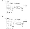
図1(A)に、本発明の液晶表示装置の構成を示す。図1(A)に示す液晶表示装置は、画素100と、比較回路101と、制御回路102と、光源103とを有する。また画素100は、液晶素子104と、スイッチング素子105と、容量素子106とを少なくとも有する。液晶素子104は、画素電極と、対向電極と、画素電極及び対向電極間の電圧が印加される液晶と、を有している。
(Embodiment 1)
FIG. 1A shows a structure of a liquid crystal display device of the present invention. A liquid crystal display device illustrated in FIG. 1A includes a pixel 100, a comparison circuit 101, a
光源103は、画素100に光を照射する機能を有する。 The light source 103 has a function of irradiating the pixel 100 with light.
スイッチング素子105は、液晶素子104の画素電極にビデオ信号の電位を与えるか否かを制御する。液晶素子104の対向電極には、所定の電位COMが与えられている。また容量素子106は一対の電極を有しており、一方の電極(第1電極)は液晶素子104の画素電極に接続されており、他方の電極(第2電極)には所定の電位GNDが与えられている。なお、本明細書において接続とは、電気的な接続と、直接的な接続とを両方含む。
The switching
スイッチング素子105がオンになると、ビデオ信号の電位Vsがスイッチング素子105を介して液晶素子104の画素電極及び容量素子106の第1電極に与えられる。よって、スイッチング素子105がオンになった当初は、液晶素子104の画素電極と対向電極間の電圧VLは、電位Vsと電位COMの差分に等しくなり、容量素子106の第1電極と第2電極間の電圧VCSは、電位Vsと電位GNDの差分と等しくなる。なお、容量素子106は必ずしも設ける必要はないが、容量素子106を設けることで、スイッチング素子105からの電荷のリークに起因する画素電極の電位の変化を防ぐことができる。
When the
そして、画素電極と対向電極の間に電圧が与えられると、液晶素子104が有する液晶内の液晶分子は、その配向が変化し始める。なお、液晶は比誘電率に異方性を有しており、液晶分子を楕円に見立てたときの長軸方向における比誘電率と、長軸方向に対して垂直方向、すなわち短軸方向における比誘電率とが異なる。よって、液晶分子の配向が変化するに従って、液晶の比誘電率にも変化が生じる。例えばメルク社製のTN液晶(商品名:MJ001393)の場合、液晶分子の長軸方向における比誘電率が8.1、短軸方向における比誘電率が3.8であり、液晶分子の配向の変化により比誘電率が最大2.1倍程度も変化する。
When a voltage is applied between the pixel electrode and the counter electrode, the orientation of liquid crystal molecules in the liquid crystal included in the
図18(A)に、ネマティック液晶を用いた場合における、液晶素子に印加される電圧(印加電圧)と比誘電率の関係を、一例として示す。ただし図18(A)は、図18(B)の断面模式図に示すように、液晶素子が画素電極3001と対向電極3002の間に液晶層3003を有する構成である場合のデータであり、液晶層3003にメルク社製の液晶(商品名:ZLI4792)を用い、セルギャップdを3.7μmとしている。また、画素電極3001面に対して液晶層3003の液晶分子が平行に配向するように予め配向処理が施されているものとする。図18から、液晶の比誘電率が液晶素子に印加される電圧に依存していることがわかる。
FIG. 18A shows, as an example, the relationship between the voltage applied to the liquid crystal element (applied voltage) and the relative dielectric constant when nematic liquid crystal is used. Note that FIG. 18A shows data in a case where the liquid crystal element has a
なお、液晶素子104を容量として見立てると、その容量値CLは、以下の式1で表すことができる。ただし、ε0は真空の誘電率、εは液晶の比誘電率、Sは液晶素子104の面積、dは液晶素子104の第1電極と第2電極間の距離(セルギャップ)を意味する。ただし、実際には配向膜の比誘電率も容量値CLの値に影響を与えるが、説明の便宜上、式1において配向膜の比誘電率は考慮しないものとする。
Incidentally, when Mitateru the
(式1)
CL=ε0×ε×S/d
(Formula 1)
C L = ε 0 × ε × S / d
そして、容量値CLと、電荷Qと、液晶素子104の画素電極と対向電極間の電圧VLの関係は、以下の式2で表すことができる。
The relationship between the capacitance value C L , the charge Q, and the voltage V L between the pixel electrode and the counter electrode of the
(式2)
Q=CL×VL
(Formula 2)
Q = C L × V L
よって、式1と式2から、以下の式3が導き出される。
Therefore, the following
(式3)
VL=d×Q/(ε0×ε×S)
(Formula 3)
V L = d × Q / (ε 0 × ε × S)
式3において、第1電極と第2電極間の距離dと、液晶素子104の面積S、真空の誘電率ε0は固定された値である。また、液晶素子104の電荷Qがリークしない理想状態であると仮定すると、電荷Qも固定された値とみなすことができる。よって、式3から、液晶分子の配向が変化することにより液晶の比誘電率εが変化すると、液晶素子104の画素電極と対向電極間の電圧VLが変化することが分かる。従って、スイッチング素子105をオンにしてビデオ信号の電位Vsを液晶素子104の画素電極に与えた後、スイッチング素子105をオフにしてからの電圧VLの変化、すなわち液晶素子104が有する画素電極の電位の変化を追跡することで、液晶分子の配向の状態を把握し、液晶分子の配向の変化が収束するタイミングを見出すことができる。
In
なお、図1(A)の場合、液晶素子104と容量素子106とが直列に接続されているため、画素電極の電位は、液晶素子104の容量値と、容量素子106の容量値の比によって定まる。例えば、ビデオ信号の電圧Vsを印加する前の状態において、液晶素子104の容量値CLと容量素子106の容量値CSの比が100:100であるとする。そして、上述したメルク社製のTN液晶(商品名:MJ001393)を液晶素子104に用いる場合、ビデオ信号の電圧Vsの印加により、最終的に液晶分子の比誘電率が最大2.1倍程度変化するため、液晶素子104の容量値CLも2.1倍に変化する。よって、ビデオ信号の電圧Vsを印加した後に液晶分子の配向の変化が収束すると、液晶素子104の容量値CLと容量素子106の容量値CSの比は210:100になる。したがって、液晶分子の配向の変化が収束すると、液晶素子104の画素電極と対向電極間の電圧VLと、容量素子106の第1電極と第2電極間の電圧VCSとの比が210:100になるように、画素電極の電位も収束する。
Note that in the case of FIG. 1A, since the
比較回路101は、画素100から与えられる液晶素子104の画素電極の電位と、基準となる電位REFとを比較し、その結果に従って互いに値の異なる2値の電位を出力する。例えば、画素電極の電位が電位REFより高い場合は電位OUT1、画素電極の電位が電位REFと同じか、それより低い場合は電位OUT2を出力する。そして電位REFを、液晶分子の配向の変化が収束したときに得られるであろう画素電極の電位と同じ高さに設定しておくことで、液晶分子の配向の変化が収束する前と後とで、比較回路101から出力される電位を切り替えることができる。なお、実際の液晶表示装置の駆動では、液晶素子104の電荷Qが多少なりともリークする。そのため、該リーク分に起因する画素電極の電位の変化分を考慮に入れて、電位REFの値を設定することが望ましい。
The comparison circuit 101 compares the potential of the pixel electrode of the
なお、図1(A)では、比較回路101としてオペアンプを用いる例を示しているが、オペアンプに限らず、画素100から与えられる電位と基準となる電位REFとを比較した結果に従って2値の電位の一つを出力することができる回路であれば、比較回路101として用いることができる。 Note that FIG. 1A illustrates an example in which an operational amplifier is used as the comparison circuit 101; however, the potential is not limited to an operational amplifier, and is a binary potential according to a result of comparing a potential supplied from the pixel 100 with a reference potential REF. Any circuit that can output one of the above can be used as the comparison circuit 101.
制御回路102は、比較回路101から出力された電位に従って、光源103の駆動を制御する。具体的には、2値の電位のうち、一方の電位が比較回路101から出力されたとき、制御回路102は光源103が点灯するように制御し、他方の電位が比較回路101から出力されたとき、制御回路102は光源103が消灯するように制御する。比較回路101から出力される電位は、液晶分子の配向の変化が収束する前と後とで、その値が切り替わるので、制御回路102は液晶分子の配向が変化するタイミングに従って、光源103の駆動を制御することができる。
The
従って、本発明では、液晶分子の配向の変化が収束するタイミングを把握できるので、該タイミングに従って光源103の駆動のタイミングを適宜設定し直すことができる。よって、液晶の応答速度が変化しても、液晶分子の配向の変化が著しい期間に光源103を消灯し、液晶分子の配向の変化が収束している期間に光源103を点灯し、動画がぼやけて視認されてしまうのを防ぐことができる。 Therefore, in the present invention, the timing at which the change in the alignment of the liquid crystal molecules converges can be grasped, and accordingly, the driving timing of the light source 103 can be appropriately set according to the timing. Therefore, even if the response speed of the liquid crystal changes, the light source 103 is turned off during a period when the change in the alignment of the liquid crystal molecules is significant, and the light source 103 is turned on during the period when the change in the alignment of the liquid crystal molecules converges. Can be prevented from being visually recognized.
なお、図1(A)では、液晶素子104の対向電極に電位COMが与えられ、容量素子106の第2電極に電位GNDが与えられている例を示しているが、液晶素子104の対向電極と容量素子106の第2電極とに、共に電位COMが与えられていても良い。この場合、液晶素子104と容量素子106とが並列に接続されていることになるので、下記の式4が成り立つ。
Note that FIG. 1A illustrates an example in which the potential COM is applied to the counter electrode of the
(式4)
VL=Q/(CL+CS)
(Formula 4)
V L = Q / (C L + C S )
液晶素子104と容量素子106とが並列に接続されている場合、例えば、ビデオ信号の電圧Vsを印加する前の状態において、液晶素子104の容量値CLと容量素子106の容量値CSの比が100:100であるとする。そして、上述したメルク社製のTN液晶(商品名:MJ001393)を液晶素子104に用いる場合、ビデオ信号の電圧Vsの印加により、最終的に液晶分子の比誘電率が最大2.1倍程度変化するため、液晶素子104の容量値CLも2.1倍に変化する。よって、ビデオ信号の電圧Vsを印加した後に液晶分子の配向の変化が収束すると、液晶素子104の容量値CLと容量素子106の容量値CSの比は210:100になる。したがって、液晶分子の配向の変化が始まる前と、液晶分子の配向の変化が収束した後とでは、液晶素子104の画素電極と対向電極間の電圧VLは、0.31倍に変化することになる。
In the case where the
液晶素子104と容量素子106の接続関係によって、液晶分子の配向の変化が収束したときに得られるであろう画素電極の電位が変化する。よって、画素100の構成に合わせて、基準となる電位REFを適宜設定すれば良い。
Depending on the connection relationship between the
次に、図1(B)に、図1(A)とは異なる、本発明の液晶表示装置の別の構成を示す。図1(B)に示す液晶表示装置は、画素200と、比較回路201と、制御回路202と、光源203とを有する。また画素200は、液晶素子204と、スイッチング素子205と、容量素子206と、容量素子207とを少なくとも有する。液晶素子204は、画素電極と、対向電極と、画素電極及び対向電極間の電圧が印加される液晶と、を有している。
Next, FIG. 1B illustrates another structure of the liquid crystal display device of the present invention, which is different from that in FIG. A liquid crystal display device illustrated in FIG. 1B includes a pixel 200, a comparison circuit 201, a
スイッチング素子205は、液晶素子204の画素電極にビデオ信号の電位を与えるか否かを制御する。液晶素子204の対向電極には、所定の電位COMが与えられている。また容量素子206は一対の電極を有しており、一方の電極(第1電極)は液晶素子204の画素電極に接続されており、他方の電極(第2電極)には所定の電位GNDが与えられている。また容量素子207は一対の電極を有しており、一方の電極(第1電極)は液晶素子204の画素電極に接続されており、他方の電極(第2電極)には所定の電位COMが与えられている。よって、図1(B)に示す液晶表示装置では、液晶素子204と容量素子206が直列に接続されており、液晶素子204と容量素子207が並列に接続されている。
The switching
スイッチング素子205がオンになると、ビデオ信号の電位Vsがスイッチング素子205を介して液晶素子204の画素電極、容量素子206の第1電極及び容量素子207の第1電極に与えられる。よって、スイッチング素子205がオンになった当初は、液晶素子204の画素電極と対向電極間の電圧VLは、電位Vsと電位COMの差分に等しくなり、容量素子206の第1電極と第2電極間の電圧VCS1は、電位Vsと電位GNDの差分と等しくなり、容量素子207の第1電極と第2電極間の電圧VCS2は、電位Vsと電位COMの差分に等しくなる。
When the
そして、画素電極と対向電極の間に電圧が与えられると、液晶素子204が有する液晶内の液晶分子は、その配向が変化し始める。そして、上述したように、液晶分子の配向が変化することにより液晶の比誘電率が変化すると、液晶素子204の画素電極と対向電極間の電圧VLが変化する。よって、スイッチング素子205をオンにしてビデオ信号の電位Vsを液晶素子204の画素電極に与えた後、スイッチング素子205をオフにしてからの電圧VLの変化、すなわち液晶素子204が有する画素電極の電位の変化を追跡することで、液晶分子の配向の状態を把握し、液晶分子の配向の変化が収束するタイミングを見出すことができる。
When a voltage is applied between the pixel electrode and the counter electrode, the orientation of liquid crystal molecules in the liquid crystal included in the
なお、図1(B)の場合、液晶素子204と容量素子206とが直列に接続されており、液晶素子204と容量素子207とが並列に接続されている。そのため、画素電極の電位は、液晶素子204の容量値と、容量素子206の容量値と、容量素子207の容量値との比によって値が定まる。
Note that in the case of FIG. 1B, the
図1(A)に示す容量素子106の容量値は、電荷のリークに起因する画素電極の電位の変化を防ぐことができる程度に、十分な大きさに設定する。しかし、液晶素子104の容量値に対して容量素子106の容量値が大きすぎると、液晶素子104の容量値が変化しても、液晶素子104の画素電極の電位の変化が小さくなり、液晶分子の配向の状態を把握しにくくなる。よって、図1(A)に示す画素100の場合、液晶素子104の画素電極の電位の変化を大きくして液晶分子の配向の状態をより明確に把握するために、容量素子106の容量値と液晶素子104の容量値とが大きく異ならないように、より望ましくは同程度になるように、設定しておくのが良い。
The capacitance value of the
一方、図1(B)に示す画素200の場合、図1(A)とは異なり、液晶素子204と直列に接続されるように容量素子206が設けられており、液晶素子204と並列に接続されるように容量素子207が設けられている。そのため、液晶素子204の電圧VLと、容量素子206の電圧VCS2との比は、液晶素子204の容量値に容量素子207の容量値を加算した値と、容量素子206の容量値との比に相当する。したがって、容量素子206の容量値を、電荷のリークに起因する画素電極の電位の変化を防ぐことができる程度に、十分な大きさに設定したとしても、容量素子207の容量値をそれに見合う程度に大きく設定することで、液晶素子204の容量値を小さく抑えつつ、液晶素子204の電圧VLと、容量素子206の電圧VCS2とが大きく異ならないように、より望ましくは同程度になるようにすることができる。よって、液晶素子204の容量値を小さく抑えつつ、液晶素子204の画素電極の電位の変化を大きくして液晶分子の配向の状態をより明確に把握することができる。
On the other hand, in the case of the pixel 200 illustrated in FIG. 1B, unlike FIG. 1A, the
比較回路201は、画素200から与えられる液晶素子204の画素電極の電位と、基準となる電位REFとを比較し、その結果に従って互いに値の異なる2値の電位を出力する。例えば、画素電極の電位が電位REFより高い場合は電位OUT1、画素電極の電位が電位REFと同じか、それより低い場合は電位OUT2を出力する。そして電位REFを、液晶分子の配向の変化が収束したときに得られるであろう画素電極の電位と同じ高さに設定しておくことで、液晶分子の配向の変化が収束する前と後とで、比較回路201から出力される電位を切り替えることができる。
The comparison circuit 201 compares the potential of the pixel electrode of the
なお、図1(B)では、比較回路201としてオペアンプを用いる例を示しているが、オペアンプに限らず、画素200から与えられる電位と基準となる電位REFとを比較した結果に従って2値の電位の一つを出力することができる回路であれば、比較回路201として用いることができる。 Note that FIG. 1B illustrates an example in which an operational amplifier is used as the comparison circuit 201; however, the potential is not limited to the operational amplifier, and is a binary potential according to a result of comparing a potential supplied from the pixel 200 with a reference potential REF. Any circuit that can output one of the two can be used as the comparison circuit 201.
制御回路202は、比較回路201から出力された電位に従って、光源203の駆動を制御する。具体的には、2値の電位のうち、一方の電位が比較回路201から出力されたとき、制御回路202は光源203が点灯するように制御し、他方の電位が比較回路201から出力されたとき、制御回路202は光源203が消灯するように制御する。比較回路201から出力される電位は、液晶分子の配向の変化が収束する前と後とで、その値が切り替わるので、制御回路202は液晶分子の配向が変化するタイミングに従って、光源203の駆動を制御することができる。
The
従って、本発明では、液晶分子の配向の変化が収束するタイミングを把握できるので、該タイミングに従って光源203の駆動のタイミングを適宜設定し直すことができる。よって、液晶の応答速度が変化しても、液晶分子の配向の変化が著しい期間に光源203を消灯し、液晶分子の配向の変化が収束している期間に光源203を点灯し、動画がぼやけて視認されてしまうのを防ぐことができる。 Therefore, in the present invention, since the timing at which the change in the alignment of the liquid crystal molecules converges can be grasped, the driving timing of the light source 203 can be appropriately set according to the timing. Therefore, even if the response speed of the liquid crystal changes, the light source 203 is turned off during a period when the change in the alignment of the liquid crystal molecules is significant, and the light source 203 is turned on during the period when the change in the alignment of the liquid crystal molecules converges. Can be prevented from being visually recognized.
なお、液晶表示装置では、焼き付きと呼ばれる液晶の劣化を防ぐために、液晶素子に印加する電圧の極性を所定のタイミングに従って反転させる交流駆動が行われることが多い。例えば、フレーム期間ごとに液晶素子に印加する電圧の極性を反転させる交流駆動を行う場合、図1(A)、図1(B)に示す本発明の液晶表示装置では、画素電極の電位の極性が同じフレーム期間においてのみ、光源の駆動のタイミングを新たに設定し直すようにし、その他のフレーム期間では、直前のフレーム期間と同じタイミングで光源を駆動させれば良い。或いは、全てのフレーム期間ごとに光源の駆動のタイミングを適宜設定し直すために、基準となる電位REFをフレーム期間ごとに変えるようにしても良いし、各極性に対応した比較回路及び制御回路を新たに設けるようにしても良い。また、極性が同じフレーム期間において、必ず光源の駆動のタイミングを設定し直す必要はない。液晶の温度変化がさほど著しくない場合などは、例えば60フレーム期間ごとに1回とするなど、光源の駆動のタイミングを設定し直す回数を、少なくしても良い。 Note that in a liquid crystal display device, in order to prevent deterioration of the liquid crystal called burn-in, AC driving is often performed to invert the polarity of a voltage applied to the liquid crystal element according to a predetermined timing. For example, in the case of performing AC driving in which the polarity of a voltage applied to a liquid crystal element is reversed every frame period, the polarity of the potential of a pixel electrode is used in the liquid crystal display device of the present invention illustrated in FIGS. However, only in the same frame period, the driving timing of the light source is newly set, and in the other frame periods, the light source may be driven at the same timing as the immediately preceding frame period. Alternatively, the reference potential REF may be changed for each frame period in order to appropriately reset the driving timing of the light source for every frame period, and a comparison circuit and a control circuit corresponding to each polarity may be provided. You may make it provide newly. Further, it is not always necessary to reset the driving timing of the light source in the frame period with the same polarity. When the temperature change of the liquid crystal is not so significant, the number of times of resetting the light source driving timing may be reduced, for example, once every 60 frame periods.
また、本発明の液晶表示装置は、画素部が画素を複数有する場合、該画素の少なくとも1つから、画素電極の電位を比較回路に出力できていればよい。図2に、本発明の液晶表示装置が有する、複数の画素300が設けられた画素部301と、比較回路302と、制御回路303と、光源304とを一例として示す。
In the liquid crystal display device of the present invention, in the case where the pixel portion includes a plurality of pixels, it is sufficient that the potential of the pixel electrode can be output from at least one of the pixels to the comparison circuit. FIG. 2 shows, as an example, a
図2において、各画素300は、信号線S1〜Sxの少なくとも1つと、走査線G1〜Gyの少なくとも1つとを有している。また画素300は、スイッチング素子として機能するトランジスタ305と、液晶素子306と、容量素子307とを有している。なお図2では、画素300において、一のトランジスタ305をスイッチング素子として用いている場合について示しているが、本発明はこの構成に限定されない。スイッチング素子としてトランジスタ以外の半導体素子を用いていても良い。或いは、複数のトランジスタをスイッチング素子として用いていても良い。
In FIG. 2, each
また図2では、図1(A)と同様に、画素300において、液晶素子306と容量素子307とが直列に接続されている場合を例示しているが、液晶素子306と容量素子307とは、並列に接続されていても良い。また図1(B)と同様に、画素300が、液晶素子306に直列に接続されている容量素子307に加えて、液晶素子306に並列に接続されている容量素子を有していても良い。
2 illustrates the case where the
図2では、複数の画素300のうち、信号線Sxと走査線Gyとを有するモニター用画素300aにおいて、液晶素子306が有する画素電極の電位をモニターするべく、該電位を比較回路302に入力する。なお、全ての画素300のうち、最も端に位置している画素300を、画素電極の電位をモニターするためのモニター用画素300aとする必要は必ずしもない。モニター用画素300aは、他の画素300と構成を変える必要はないので、いずれの画素300をモニター用画素300aとして用いるかは、設計者が適宜決めることができる。また、画素部301が有する複数の画素300のうち、実際の映像の表示には用いることのないダミー用の画素の一つを、モニター用画素300aとして用いるようにしても良い。ただし、いずれの場合にせよ、全ての画素300のうち、最後にビデオ信号の入力が行われる画素において、液晶分子の配向の変化が収束するタイミングが最も遅くなる。よって、最後にビデオ信号の入力が行われる画素の一つをモニター用画素300aとして用いることで、全ての画素300において液晶分子の配向の変化が収束するタイミングを把握することができ、望ましい。
In FIG. 2, in the
次に、図2に示す画素部301の動作と、光源304の駆動について説明する。まず、走査線G1〜Gyが順に選択されると、選択された走査線を有する画素300において、トランジスタ305がオンになる。そして信号線S1〜Sxに、順にまたは同時にビデオ信号の電位が与えられると、オンのトランジスタ305を介して、ビデオ信号の電位が液晶素子306の画素電極に与えられる。次に走査線の選択が終了すると、該走査線を有する画素300において、トランジスタ305がオフになる。そして液晶素子306は、液晶分子の配向の変化に伴い、その画素電極の電位が変化する。
Next, operation of the
図3に、画素部301における、ビデオ信号の画素300への入力のタイミングを示す。図3では、横軸は時間を示しており、縦軸は走査線が選択される方向(走査方向)を示している。また、図3において、光源304の点灯期間は白地で示し、消灯期間はハッチで示す。期間Taは、最初の走査線が選択されてから最後の走査線が選択されるまでの期間を意味しており、期間Ta内に全ての画素300にビデオ信号が入力される。
FIG. 3 shows the input timing of the video signal to the
期間Taでは、複数の画素300に順にビデオ信号が入力されている最中なので、画素300によっては液晶素子306が有する液晶分子の配向の変化が著しい。また、期間Taにおいて最後にビデオ信号が入力される画素300では、他の画素300に比べて、液晶分子の配向の変化が収束するタイミングは最も遅い。そして、液晶分子の配向の変化が収束するタイミングは、液晶の温度によっても随時変わってくる。
In the period Ta, since video signals are being sequentially input to the plurality of
図4(A)と図4(B)に、最後にビデオ信号が入力される画素300における、液晶素子306の透過率の時間変化と、光源の駆動のタイミングを示す。図4(A)、(B)では、横軸は時間を示し、縦軸は液晶素子306の透過率を示す。また、光源304の点灯時間は白地で示し、消灯期間はハッチで示す。また図4(C)には、信号線に入力される電位の時間変化も併せて示す。ただし、図4(C)では、信号線に与えられる電位が、第1フレーム期間と第3フレーム期間において電位COMよりも高く、第2フレーム期間では電位COMと同じである場合を例示している。
4A and 4B show a temporal change in the transmittance of the
図4(A)と図4(B)の透過率の変化は、共に図4(C)に示すタイミングチャートに同期している。しかし、図4(A)と図4(B)とでは、温度変化により液晶の比誘電率が異なっており、透過率の変化が著しい期間401の長さが異なっている。より詳細に説明すると、図4(A)の方が図4(B)よりも、期間401が短く、期間402が長くなっている。
4A and 4B are both synchronized with the timing chart shown in FIG. 4C. However, in FIG. 4A and FIG. 4B, the relative permittivity of the liquid crystal is different depending on the temperature change, and the length of the
本発明では、モニター用画素300aが有する液晶素子306の画素電極の電位から、液晶分子の配向の変化が収束するタイミングを把握することができる。そして、制御回路303は、画素300へのビデオ信号の入力が開始されてから、全ての画素300において液晶分子の配向の変化が収束するまでの期間Tb(図3参照)において、光源304が消灯するように、光源304の駆動を制御する。よって本発明では、図4(A)と図4(B)のいずれの場合においても、少なくとも期間401において消灯するように光源304を駆動させることができる。期間Tbにおいて光源304を消灯にしておくことで、液晶分子の配向の変化、すなわち液晶素子の透過率の変化が視認されにくくなり、動画がぼやけて見えるのを防ぐことができる。
In the present invention, the timing at which the change in alignment of liquid crystal molecules converges can be grasped from the potential of the pixel electrode of the
なお、期間401は、液晶の比誘電率のみならず、液晶素子に印加される電圧の変化量によっても異なる。例えばVA液晶の場合だと、黒表示から中間階調表示に移行する際に液晶の応答速度が最も遅くなるため、期間401が最長となる。よって、光源304の駆動のタイミングを設定する際、まず先のフレーム期間において黒表示を行った後、次の第2のフレーム期間において中間階調表示を行うように、モニター用画素300aにビデオ信号を入力する。そして、上記第2のフレーム期間における画素電極の電位を用いて光源304の駆動のタイミングを設定するのが望ましい。上記構成により、いずれの階調を表示する場合でも、液晶分子の配向の変化が収束するまでの期間Tbにおいて光源304が消灯するように光源304の駆動を制御し、動画がぼやけて見えるのを防ぐことができる。
Note that the
なお、VA液晶の場合だと、黒表示から中間階調表示に移行する際に液晶の応答速度が最も遅くなるが、液晶の応答速度が最も遅くなる表示のパターンは液晶の種類によって異なる。よって、液晶の種類に合わせて、光源304の駆動のタイミングを設定する際に、応答速度が最長となるよう、モニター用画素300aにおいて階調が変化する表示パターンを、適宜選択すればよい。例えばTN液晶、OCB液晶の場合、白表示から中間階調表示に移行する際に液晶の応答速度が最も遅くなる。よって、この場合、白表示の次に中間階調表示を行う表示パターンを用いて、光源304の駆動のタイミングを設定するのが望ましい。また、例えばIPS液晶の場合、VA液晶と同様に、黒表示から中間階調表示に移行する際に液晶の応答速度が最も遅くなる。よって、この場合、黒表示の次に中間階調表示を行う表示パターンを用いて、光源304の駆動のタイミングを設定するのが望ましい。
In the case of the VA liquid crystal, the response speed of the liquid crystal becomes the slowest when shifting from the black display to the halftone display, but the display pattern in which the response speed of the liquid crystal becomes the slowest differs depending on the type of the liquid crystal. Therefore, when setting the driving timing of the light source 304 in accordance with the type of liquid crystal, a display pattern whose gradation changes in the
また、図4(A)、図4(B)では、期間401のみならず期間403においても液晶分子の配向の変化が著しい。期間401は、液晶素子の画素電極の電位が、対向電極の電位からより離れた電位に変化する際に起こる、液晶分子の配向の変化の著しい期間である。一方、期間403は、液晶素子の画素電極の電位が、対向電極の電位により近い電位に変化する際に起こる、液晶分子の配向の変化の著しい期間である。本実施の形態では、期間401における画素電極の電位の変化を用い、光源304の駆動のタイミングを設定しているが、期間403における画素電極の電位の変化を用いて、光源304の駆動のタイミングを設定しても良い。液晶の種類にもよるが、期間401よりも期間403の方が長くなる場合がある。よって、期間401よりも期間403の方が長くなる場合は、期間403における画素電極の電位の変化を用いて、光源304の駆動のタイミングを設定することで、より確実に動画がぼやけて見えるのを防ぐことができる。
4A and 4B, the change in the alignment of liquid crystal molecules is significant not only in the
なお、期間403において光源304の駆動のタイミングを設定する場合も、期間403が最長となる表示パターンを用いるのが望ましい。例えばVA液晶の場合だと、白表示から黒表示に移行する際に、液晶の応答時間が最も長くなり、期間401が最長となる。よって、光源304の駆動のタイミングを設定する際、まず先のフレーム期間において白表示を行った後、次の第2のフレーム期間において黒表示を行うように、モニター用画素300aにビデオ信号を入力する。そして、上記第2のフレーム期間における画素電極の電位を用いて光源304の駆動のタイミングを設定するのが望ましい。上記構成により、いずれの階調を表示する場合でも、液晶分子の配向の変化が収束するまでの期間Tbにおいて光源304が消灯するように光源304の駆動を制御し、動画がぼやけて見えるのを防ぐことができる。
Note that also in the case where the driving timing of the light source 304 is set in the
なお、VA液晶の場合だと、白表示から黒表示に移行する際に液晶の応答時間が最も長くなるが、液晶の応答時間が最も長くなる表示のパターンは液晶の種類によって異なる。よって、液晶の種類に合わせて、光源304の駆動のタイミングを設定する際の、表示パターンを適宜選択すればよい。例えばTN液晶、OCB液晶の場合、黒表示から白表示に移行する際に液晶の応答速度が最も遅くなる。よって、この場合、黒表示の次に白表示を行う表示パターンを用いて、光源304の駆動のタイミングを設定するのが望ましい。また、例えばIPS液晶の場合、VA液晶と同様に、白表示から黒表示に移行する際に液晶の応答速度が最も遅くなる。よって、この場合、白表示の次に黒表示を行う表示パターンを用いて、光源304の駆動のタイミングを設定するのが望ましい。 In the case of the VA liquid crystal, the response time of the liquid crystal becomes the longest when shifting from the white display to the black display, but the display pattern in which the response time of the liquid crystal becomes the longest varies depending on the type of the liquid crystal. Therefore, a display pattern for setting the drive timing of the light source 304 may be selected as appropriate in accordance with the type of liquid crystal. For example, in the case of TN liquid crystal and OCB liquid crystal, the response speed of the liquid crystal becomes the slowest when shifting from black display to white display. Therefore, in this case, it is desirable to set the driving timing of the light source 304 using a display pattern that performs white display next to black display. For example, in the case of the IPS liquid crystal, the response speed of the liquid crystal becomes the slowest when shifting from the white display to the black display, similarly to the VA liquid crystal. Therefore, in this case, it is desirable to set the driving timing of the light source 304 using a display pattern that performs black display next to white display.
また、図1(A)では光源103を一つだけ図示している。図1(B)では光源203を一つだけ図示している。図2では光源304を一つだけ図示している。しかし、本発明はこれらの構成に限定されない。光源103と、光源203と、光源304とは、その数がそれぞれ単数であっても良いが、複数であっても良い。 In FIG. 1A, only one light source 103 is shown. In FIG. 1B, only one light source 203 is shown. In FIG. 2, only one light source 304 is shown. However, the present invention is not limited to these configurations. The light source 103, the light source 203, and the light source 304 may be singular or plural.
なお、本実施の形態では、アクティブマトリクス型の液晶表示装置を例に挙げて説明したが、本発明の液晶表示装置はパッシブマトリクス型であっても良い。 Note that although an active matrix liquid crystal display device is described as an example in this embodiment mode, the liquid crystal display device of the present invention may be a passive matrix liquid crystal display device.
(実施の形態2)
本実施の形態では、本発明の液晶表示装置が有する制御回路の具体的な構成の一例について説明する。
(Embodiment 2)
In this embodiment, an example of a specific structure of a control circuit included in the liquid crystal display device of the present invention will be described.
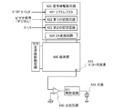
図5(A)は、本発明の液晶表示装置が有する比較回路501と、制御回路502と、光源503とを示している。図5(A)に示す制御回路502は、記憶回路504と、スイッチング回路505とを少なくとも有している。
FIG. 5A shows a comparison circuit 501, a control circuit 502, and a light source 503 included in the liquid crystal display device of the present invention. A control circuit 502 illustrated in FIG. 5A includes at least a
比較回路501は、画素から与えられる液晶素子の画素電極の電位VEと、基準となる電位REFとが入力されている。そして比較回路501は電位VEと電位REFとを比較し、その結果に従って互いに値の異なる電位OUT1または電位OUT2を出力する。 Comparator circuit 501, the potential V E of the pixel electrodes of the liquid crystal element applied from the pixel, the potential REF serving as a reference is input. The comparator circuit 501 compares the potential V E and the potential REF, and outputs different potentials OUT1 or potential OUT2 its value with each other accordingly.
制御回路502では、比較回路501から出力された電位が、電位OUT1と電位OUT2のうちのいずれであるかを、記憶回路504においてデータとして記憶する。記憶回路504には、記憶回路504に記憶されているデータを保持するための電源電位VDDと、記憶が行われるタイミングを制御する信号SigLとが入力されている。具体的には、信号SigLによって、光源503の駆動のタイミングを設定する際に、記憶回路504に新たにデータが書き込まれるようになる。また逆に、信号SigLによって、光源503の駆動のタイミングを設定された状態のまま維持する際に、記憶回路504に新たにデータが書き込まれないようになる。なお、全ての画素のうち、最初の画素にビデオ信号が入力されるタイミングが信号SigLによって制御されている場合、該信号SigLを用いることで、上記最初の画素にビデオ信号が入力されるタイミングに合わせて、光源503を消灯させるタイミングをも制御することができる。
In the control circuit 502, the
光源の駆動のタイミングを設定するタイミングは、上述したように設計者が適宜決めることができる。具体的には、信号SigLまたはその他の制御信号を用いることで、光源503の駆動のタイミングを設定するタイミングを、リアルタイムに制御することができる。なお、光源の駆動のタイミングを、毎フレーム期間ごとにリアルタイムで設定し直すのではなく、複数のフレーム期間ごとに設定し直す場合、制御回路502内にタイミング検出用回路を更に設け、設定された光源503の駆動のタイミングを次回の設定時まで、上記タイミング検出用回路で記憶するようにしても良い。例えばタイミング検出用回路は、光源503の駆動のタイミングを設定し直すように指示が来たら、比較回路501から出力される電位を用いて、1フレーム期間が開始されてから全ての画素において液晶分子の配向の変化が収束するまでの期間を検出するための回路と、各フレーム期間が開始されてからの時間を計測するための回路と、上記2つの回路から出力される信号に従って、記憶回路504のデータを書き換える回路と、を用いれば良い。
The timing for setting the timing of driving the light source can be appropriately determined by the designer as described above. Specifically, by using the signal Sig L or another control signal, the timing for setting the driving timing of the light source 503 can be controlled in real time. If the timing of driving the light source is not reset in real time every frame period but is reset every frame period, a timing detection circuit is further provided in the control circuit 502 and set. The timing for driving the light source 503 may be stored in the timing detection circuit until the next setting. For example, when the timing detection circuit is instructed to reset the driving timing of the light source 503, the potential output from the comparison circuit 501 is used for the liquid crystal molecules in all the pixels after the start of one frame period. A
スイッチング回路505は、記憶回路504において記憶されているデータに従ってスイッチングを行うことで、光源503への電力の供給を制御する。なお図5(A)では、スイッチング回路505に、トランジスタを一つ用いている例を示しているが、本発明はこの構成に限定されない。スイッチング回路505に、トランジスタ以外の半導体素子を用いていても良いし、複数のトランジスタを用いていても良い。また記憶回路504として、ラッチ回路などを用いることができる。光源503として、LEDを用いることができる。ただし本発明の液晶表示装置に用いることができる光源は、必ずしもLEDに限定されない。LEDのように点灯と消灯を高速で切り替えることが可能な発光素子であれば、本発明の液晶表示装置の光源として用いることは可能である。
The
なお、本実施の形態では、記憶回路504を有している制御回路502の構成について説明したが、本発明の液晶表示装置が有する制御回路は、必ずしも記憶回路を用いる必要はない。記憶回路を用いない場合は、制御回路502において、比較回路501の後段にスイッチング回路505が設けられる。そして記憶回路を用いない場合、全てのフレーム期間ごとに光源の駆動のタイミングを適宜設定し直すことになるので、基準となる電位REFをフレーム期間ごとに変えるか、若しくは各極性に対応した比較回路及び制御回路を新たに設けるようにする。
Note that although the structure of the control circuit 502 including the
なお制御回路502は、図5(A)に示した構成に加え、バッファを有していても良い。図5(B)に、比較回路501と、バッファ506をさらに有する制御回路502と、光源503とを示す。図5(B)に示す制御回路502では、記憶回路504から出力される電位を、バッファ506を介して制御回路502に入力している。バッファ506を用いることで、スイッチング回路505におけるスイッチングの制御に大電力が必要な場合でも、確実にそのスイッチングを制御することができる。
Note that the control circuit 502 may include a buffer in addition to the structure illustrated in FIG. FIG. 5B illustrates a comparison circuit 501, a control circuit 502 further including a
なお、図5に示した構成の制御回路502が有する機能は、比較回路501において検出された電位を用い、CPU(central processing unit)で行うことも可能である。ただし本発明では、CPUを用いた複雑な制御系の回路を使用せずに、液晶の応答速度に合わせて光源503の駆動を制御することができるというメリットを有する。或いは本発明では、CPUを使用していたとしても、CPUの負荷を低減させつつ、液晶の応答速度に合わせて光源503の駆動を制御することができるというメリットを有する。 Note that the function of the control circuit 502 having the configuration illustrated in FIG. 5 can be performed by a CPU (central processing unit) using the potential detected by the comparison circuit 501. However, the present invention has an advantage that the driving of the light source 503 can be controlled in accordance with the response speed of the liquid crystal without using a complicated control system circuit using a CPU. Or even if it uses CPU, in this invention, it has the merit that the drive of the light source 503 can be controlled according to the response speed of a liquid crystal, reducing the load of CPU.
なお、図5(A)、図5(B)では、光源503を一つだけ図示しているが、本発明はこの構成に限定されない。光源503は、その数が単数であっても良いが、複数であっても良い。 Note that although only one light source 503 is illustrated in FIGS. 5A and 5B, the present invention is not limited to this structure. The number of the light sources 503 may be singular or plural.
本実施の形態は、上記実施の形態と適宜組み合わせて実施することが可能である。 This embodiment can be implemented in combination with any of the above embodiments as appropriate.
(実施の形態3)
本実施の形態では、本発明の液晶表示装置の全体的な構成の一例について説明する。図6に、本発明の液晶表示装置のブロック図を示す。
(Embodiment 3)
In this embodiment, an example of the entire structure of the liquid crystal display device of the present invention will be described. FIG. 6 shows a block diagram of the liquid crystal display device of the present invention.
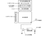
図6に示す液晶表示装置は、液晶素子を備えた画素を複数有する画素部600と、各画素をラインごとに選択する走査線駆動回路610と、選択されたラインの画素へのビデオ信号の入力を制御する信号線駆動回路620と、比較回路630と、制御回路631と、光源632とを有する。そして本発明では画素部600が有する画素のうち、いずれか1つをモニター用画素633として用いる。モニター用画素633の画素電極の電位は、比較回路630に与えられる。
A liquid crystal display device illustrated in FIG. 6 includes a pixel portion 600 having a plurality of pixels each including a liquid crystal element, a scanning
図6において信号線駆動回路620は、シフトレジスタ621、第1の記憶回路622、第2の記憶回路623、DA(Digital to Analog)変換回路624を有している。シフトレジスタ621には、クロック信号S−CLK、スタートパルス信号S−SPが入力される。シフトレジスタ621は、これらクロック信号S−CLK及びスタートパルス信号S−SPに従って、パルスが順次シフトするタイミング信号を生成し、第1の記憶回路622に出力する。タイミング信号のパルスの出現する順序は、走査方向切り替え信号に従って切り替えるようにしても良い。 In FIG. 6, the signal line driver circuit 620 includes a shift register 621, a first memory circuit 622, a second memory circuit 623, and a DA (Digital to Analog) converter circuit 624. A clock signal S-CLK and a start pulse signal S-SP are input to the shift register 621. The shift register 621 generates a timing signal for sequentially shifting the pulses in accordance with the clock signal S-CLK and the start pulse signal S-SP, and outputs the timing signal to the first memory circuit 622. The order in which the pulses of the timing signal appear may be switched according to the scanning direction switching signal.
第1の記憶回路622にタイミング信号が入力されると、該タイミング信号のパルスに従って、ビデオ信号が順に第1の記憶回路622に書き込まれ、保持される。なお、第1の記憶回路622が有する複数の記憶素子に順にビデオ信号を書き込んでも良いが、第1の記憶回路622が有する複数の記憶素子をいくつかのグループに分け、該グループごとに並行してビデオ信号を入力する、いわゆる分割駆動を行っても良い。なおこのときのグループ数を分割数と呼ぶ。例えば4つの記憶素子ごとにグループに分けた場合、4分割で分割駆動することになる。 When a timing signal is input to the first memory circuit 622, video signals are sequentially written and held in the first memory circuit 622 in accordance with the pulse of the timing signal. Note that the video signal may be written in order to the plurality of storage elements included in the first storage circuit 622; however, the plurality of storage elements included in the first storage circuit 622 are divided into several groups and are parallel to each group. In other words, so-called divided driving, in which a video signal is input, may be performed. Note that the number of groups at this time is called the number of divisions. For example, when four memory elements are divided into groups, the driving is divided into four.
第1の記憶回路622の全ての記憶素子への、ビデオ信号の書き込みが一通り終了するまでの時間を、ライン期間と呼ぶ。実際には、上記ライン期間に水平帰線期間が加えられた期間をライン期間に含むことがある。 The time until video signal writing to all the memory elements of the first memory circuit 622 is completed is called a line period. Actually, the line period may include a period in which a horizontal blanking period is added to the line period.
1ライン期間が終了すると、第2の記憶回路623に入力されるラッチ信号S−LSのパルスに従って、第1の記憶回路622に保持されているビデオ信号が、第2の記憶回路623に一斉に書き込まれ、保持される。ビデオ信号を第2の記憶回路623に送出し終えた第1の記憶回路622には、再びシフトレジスタ621からのタイミング信号に従って、次のビデオ信号の書き込みが順次行われる。この2順目の1ライン期間中には、第2の記憶回路623に書き込まれ、保持されているビデオ信号が、DA変換回路624に入力される。 When one line period ends, video signals held in the first memory circuit 622 are simultaneously transmitted to the second memory circuit 623 in accordance with the pulse of the latch signal S-LS input to the second memory circuit 623. Written and retained. In the first memory circuit 622 that has finished sending the video signal to the second memory circuit 623, the next video signal is sequentially written in accordance with the timing signal from the shift register 621 again. During the second line period, the video signal written and held in the second memory circuit 623 is input to the DA converter circuit 624.
そしてDA変換回路624は、入力されたデジタルのビデオ信号をアナログのビデオ信号に変換し、信号線を介して画素部600内の各画素に入力する。 The DA conversion circuit 624 converts the input digital video signal into an analog video signal, and inputs the analog video signal to each pixel in the pixel portion 600 through a signal line.
なお信号線駆動回路620は、シフトレジスタ621の代わりに、パルスが順次シフトする信号を出力することができる別の回路を用いても良い。 Note that the signal line driver circuit 620 may use another circuit that can output a signal in which a pulse is sequentially shifted instead of the shift register 621.
なお図6ではDA変換回路624の後段に画素部600が直接接続されているが、本発明はこの構成に限定されない。画素部600の前段に、DA変換回路624から出力されたビデオ信号に信号処理を施す回路を設けることができる。信号処理を施す回路の一例として、例えば波形を整形することができるバッファなどが挙げられる。 In FIG. 6, the pixel portion 600 is directly connected to the subsequent stage of the DA converter circuit 624, but the present invention is not limited to this configuration. A circuit that performs signal processing on the video signal output from the DA converter circuit 624 can be provided in the preceding stage of the pixel portion 600. An example of a circuit that performs signal processing includes a buffer that can shape a waveform, for example.
次に、走査線駆動回路610の動作について説明する。本発明の液晶表示装置では、画素部600の各画素に走査線が複数設けられている。走査線駆動回路610は選択信号を生成し、該選択信号を複数の各走査線に入力することで、画素をラインごとに選択する。選択信号により画素が選択されると、該画素が有するスイッチング素子がオンになり、画素へのビデオ信号の入力が行われる。
Next, the operation of the scan
なお、本実施の形態では複数の走査線に入力される選択信号を、全て一の走査線駆動回路610で生成している例について述べたが、本発明はこの構成に限定されない。複数の走査線駆動回路610で複数の走査線に入力される選択信号の生成を行うようにしても良い。
Note that although an example in which selection signals input to a plurality of scanning lines are all generated by one scanning
また、画素部600、走査線駆動回路610、信号線駆動回路620、比較回路630、制御回路631は、同一基板上に形成することができるが、いずれかを異なる基板上に形成することもできる。
In addition, the pixel portion 600, the scan
また、図6では、光源632を一つだけ図示しているが、本発明はこの構成に限定されない。光源632は、その数が単数であっても良いが、複数であっても良い。 In FIG. 6, only one light source 632 is illustrated, but the present invention is not limited to this configuration. The number of light sources 632 may be singular or plural.
次に図7に、図6とは異なる、本実施の形態の液晶表示装置のブロック図を一例として示す。 Next, FIG. 7 shows a block diagram of the liquid crystal display device of this embodiment, which is different from FIG. 6, as an example.
図7に示す本発明の液晶表示装置は、複数の画素を有する画素部640と、複数の画素をラインごとに選択することができる走査線駆動回路650と、選択されたライン内の画素へのビデオ信号の入力を制御する信号線駆動回路660と、比較回路670と、制御回路671と、光源672とを有する。そして本発明では画素部640が有する画素のうち、いずれか1つをモニター用画素673として用いる。モニター用画素673の画素電極の電位は、比較回路670に与えられる。
The liquid crystal display device of the present invention shown in FIG. 7 includes a pixel portion 640 having a plurality of pixels, a scanning
信号線駆動回路660は、シフトレジスタ661と、サンプリング回路662と、アナログ信号を記憶することができる記憶回路663とを少なくとも有する。シフトレジスタ661にクロック信号S−CLKと、スタートパルス信号S−SPが入力されると、シフトレジスタ661はこれらクロック信号S−CLK及びスタートパルス信号S−SPに従って、パルスが順次シフトするタイミング信号を生成し、サンプリング回路662に入力する。サンプリング回路662では、入力されたタイミング信号に従って、信号線駆動回路660に入力された1ライン期間分のアナログのビデオ信号をサンプリングする。そして1ライン期間分のビデオ信号が全てサンプリングされると、サンプリングされたビデオ信号はラッチ信号S−LSに従って一斉に記憶回路663に出力され、保持される。記憶回路663に保持されるビデオ信号は、信号線を介して画素部640に入力される。 The signal line driver circuit 660 includes at least a shift register 661, a sampling circuit 662, and a storage circuit 663 that can store an analog signal. When the clock signal S-CLK and the start pulse signal S-SP are input to the shift register 661, the shift register 661 generates a timing signal for sequentially shifting the pulses in accordance with the clock signal S-CLK and the start pulse signal S-SP. It is generated and input to the sampling circuit 662. The sampling circuit 662 samples an analog video signal for one line period input to the signal line driver circuit 660 in accordance with the input timing signal. When all the video signals for one line period are sampled, the sampled video signals are output to the memory circuit 663 all at once according to the latch signal S-LS and held. A video signal held in the memory circuit 663 is input to the pixel portion 640 through a signal line.
なお本実施の形態では、サンプリング回路662において1ライン期間分のビデオ信号を全てサンプリングした後に、一斉に下段の記憶回路663にサンプリングされたビデオ信号を入力する場合を例に挙げて説明するが、本発明はこの構成に限定されない。サンプリング回路662において各画素に対応するビデオ信号をサンプリングしたら、1ライン期間を待たずに、その都度下段の記憶回路663にサンプリングされたビデオ信号を入力しても良い。 Note that in this embodiment, a case where the sampling circuit 662 samples all video signals for one line period and then inputs the sampled video signals to the lower storage circuit 663 will be described as an example. The present invention is not limited to this configuration. If the sampling circuit 662 samples the video signal corresponding to each pixel, the sampled video signal may be input to the lower storage circuit 663 without waiting for one line period.
またビデオ信号のサンプリングは対応する画素毎に順に行っても良いし、1ライン内の画素をいくつかのグループに分け、各グループに対応する画素ごとに並行して行っても良い。 The sampling of the video signal may be performed in order for each corresponding pixel, or the pixels in one line may be divided into several groups and performed in parallel for each pixel corresponding to each group.
なお図7では記憶回路663の後段に直接画素部640が接続されているが、本発明はこの構成に限定されない。画素部640の前段に、記憶回路663から出力されたアナログのビデオ信号に信号処理を施す回路を設けることができる。信号処理を施す回路の一例として、例えば波形を整形することができるバッファなどが挙げられる。 Note that in FIG. 7, the pixel portion 640 is directly connected to the subsequent stage of the memory circuit 663; however, the present invention is not limited to this structure. A circuit that performs signal processing on the analog video signal output from the memory circuit 663 can be provided in the previous stage of the pixel portion 640. An example of a circuit that performs signal processing includes a buffer that can shape a waveform, for example.
そして、記憶回路663から画素部640にビデオ信号が入力されるのと並行して、サンプリング回路662は次のライン期間に対応するビデオ信号を再びサンプリングすることができる。 In parallel with the input of the video signal from the memory circuit 663 to the pixel portion 640, the sampling circuit 662 can sample the video signal corresponding to the next line period again.
次に、走査線駆動回路650の動作について説明する。本発明の液晶表示装置では、画素部640の各画素に走査線が複数設けられている。走査線駆動回路650は選択信号を生成し、該選択信号を複数の各走査線に入力することで、画素をラインごとに選択する。選択信号により画素が選択されると、該画素が有するスイッチング素子がオンになり、画素へのビデオ信号の入力が行われる。
Next, the operation of the scanning
なお、本実施の形態では複数の走査線に入力される選択信号を、全て一の走査線駆動回路650で生成している例について述べたが、本発明はこの構成に限定されない。複数の走査線駆動回路650で複数の走査線に入力される選択信号の生成を行うようにしても良い。
Note that although an example in which selection signals input to a plurality of scanning lines are all generated by one scanning
また、画素部640、走査線駆動回路650、信号線駆動回路660、比較回路670、制御回路671は、同一基板上に形成することができるが、いずれかを異なる基板上に形成することもできる。
The pixel portion 640, the scan
また、図7では、光源672を一つだけ図示しているが、本発明はこの構成に限定されない。光源672は、その数が単数であっても良いが、複数であっても良い。 In FIG. 7, only one light source 672 is shown, but the present invention is not limited to this configuration. The number of the light sources 672 may be singular or plural.
本実施の形態は、上記実施の形態と適宜組み合わせて実施することが可能である。 This embodiment can be implemented in combination with any of the above embodiments as appropriate.
(実施の形態4)
本実施の形態では、液晶表示装置が置かれる環境下の輝度を検出し、検出された輝度に合わせて光源の輝度を調整する液晶表示装置の構成について説明する。
(Embodiment 4)
In this embodiment, a configuration of a liquid crystal display device that detects luminance in an environment where the liquid crystal display device is placed and adjusts luminance of a light source according to the detected luminance will be described.
図8(A)に、本実施の形態の液晶表示装置が有する、光源801の制御系の回路の一例を示す。図8(A)に示す光源801の制御系の回路は、比較回路802、制御回路803、光検出器804、信号生成回路805、輝度制御回路806を有する。
FIG. 8A illustrates an example of a circuit of a control system for the light source 801 included in the liquid crystal display device of this embodiment. A control circuit of the light source 801 illustrated in FIG. 8A includes a comparison circuit 802, a control circuit 803, a
比較回路802は、画素から与えられる液晶素子の画素電極の電位VEと、基準となる電位REFとを比較し、その結果に従って互いに値の異なる2値の電位を出力する。制御回路803は、比較回路802から出力された電位に従って、光源801の駆動を制御する。具体的には、2値の電位のうち、一方の電位が比較回路802から出力されたとき、制御回路803は光源801が点灯するように制御し、他方の電位が比較回路802から出力されたとき、制御回路803は光源801が消灯するように制御する。比較回路802から出力される電位は、液晶分子の配向の変化が収束する前と後とで、その値が切り替わるので、制御回路803は液晶分子の配向が変化するタイミングに従って、光源801の駆動を制御することができる。 Comparator circuit 802 compares the potential V E of the pixel electrodes of the liquid crystal element applied from pixels, a reference and potential REF, and outputs the potential of the two different values of the mutually values accordingly. The control circuit 803 controls driving of the light source 801 in accordance with the potential output from the comparison circuit 802. Specifically, when one of the binary potentials is output from the comparison circuit 802, the control circuit 803 controls the light source 801 to be turned on, and the other potential is output from the comparison circuit 802. At this time, the control circuit 803 controls the light source 801 to turn off. Since the potential output from the comparison circuit 802 changes before and after the change in the alignment of the liquid crystal molecules converges, the control circuit 803 drives the light source 801 in accordance with the timing at which the alignment of the liquid crystal molecules changes. Can be controlled.
光検出器804は、液晶表示装置が置かれる環境下の輝度または光強度を検出し、該輝度または光強度の情報を含む電気信号(第1の信号)を生成することができる。光検出器804として、例えばフォトダイオード、フォトトランジスタ、電荷結合素子(CCD:Charge Coupled Device)などの、光を電気エネルギーに変換する光電変換素子を用いることができる。
The
信号生成回路805は、光検出器804で生成される電気信号を用い、検出された輝度の情報に従って光源801の輝度を決める。図8(A)では、信号生成回路805が積分回路807と、輝度比較回路808とを有する例を示している。
The signal generation circuit 805 uses the electrical signal generated by the
積分回路807は光検出器804において検出された光強度を時間で積分する。人間は、一定時間内の光強度を積分して知覚するという特性を有しているので、積分回路807を用いることで、人間の目が感じる輝度を算出することができる。輝度比較回路808は、積分回路807によって算出された輝度と、あらかじめ設定しておいた基準となる輝度とを比較する。
The integrating
そして、比較の結果が情報として含まれる信号(第2の信号)を出力する。輝度制御回路806は、上記第2の信号を、光源の輝度を調整するための信号として用い、輝度比較回路808における比較の結果に従って光源801の輝度の制御を行う。具体的には、算出された輝度が設定された輝度よりも高い場合、光源801の輝度がより高くなるように、逆に算出された輝度が設定された輝度よりも低い場合、光源801の輝度がより低くなるように、第2の信号に従って光源801の輝度の制御を行う。
Then, a signal (second signal) including the comparison result as information is output. The
よって本実施の形態の液晶表示装置では、液晶表示装置が置かれる環境下の輝度が高い場合に光源801の輝度を高め、逆に環境下の輝度が低い場合に光源801の輝度を低くすることができる。上記構成により、明るい場所では液晶表示装置に表示される映像を明るくすることで見やすくし、逆に、暗い場所では映像の明るさを抑えて消費電力を低減させることができる。 Therefore, in the liquid crystal display device of this embodiment, the luminance of the light source 801 is increased when the luminance in the environment where the liquid crystal display device is placed is high, and conversely, the luminance of the light source 801 is decreased when the luminance in the environment is low. Can do. With the above configuration, it is possible to make the image displayed on the liquid crystal display device brighter in a bright place to make it easier to see, and conversely, in a dark place, the brightness of the image can be suppressed to reduce power consumption.
なお、基準となる輝度は必ずしも1つである必要はなく、基準となる輝度が複数設定されていても良い。例えば、輝度の低い順から第1の輝度、第2の輝度、第3の輝度というように、3つの基準となる輝度が設定されていている場合、点灯時の光源801の輝度を4段階に調整できるようにする。そして、算出された輝度が第1の輝度よりも低い時は、4段階のうち最も低い輝度になるように、第2の信号に従って光源801を点灯させる。また、算出された輝度が第1の輝度よりも高く、第2の輝度よりも低い時は、4段階のうち2番目に低い輝度になるように、第2の信号に従って光源801を点灯させる。また、算出された輝度が第2の輝度よりも高く、第3の輝度よりも低い時は、4段階のうち2番目に高い輝度になるように、第2の信号に従って光源801を点灯させる。また、算出された輝度が第3の輝度よりも高い時は、4段階のうち最も高い輝度になるように、第2の信号に従って光源801を点灯させる。 Note that the reference luminance is not necessarily one, and a plurality of reference luminances may be set. For example, when three reference luminances such as the first luminance, the second luminance, and the third luminance are set in order from the lowest luminance, the luminance of the light source 801 during lighting is set to four levels. Allow adjustment. When the calculated luminance is lower than the first luminance, the light source 801 is turned on according to the second signal so that the lowest luminance among the four levels is obtained. In addition, when the calculated luminance is higher than the first luminance and lower than the second luminance, the light source 801 is turned on according to the second signal so that the luminance is the second lowest among the four levels. Further, when the calculated luminance is higher than the second luminance and lower than the third luminance, the light source 801 is turned on according to the second signal so that the luminance is the second highest among the four levels. When the calculated luminance is higher than the third luminance, the light source 801 is turned on according to the second signal so that the highest luminance among the four levels is obtained.
さらに、本実施の形態の液晶表示装置では、上記効果に加え、液晶分子の配向の変化が収束するタイミングを把握できるので、該タイミングに従って光源801の駆動のタイミングを適宜設定し直すことができる。よって、液晶の応答速度が変化しても、液晶分子の配向の変化が著しい期間に光源801を消灯し、液晶分子の配向の変化が収束している期間に光源801を点灯し、動画がぼやけて視認されてしまうのを防ぐことができる。 Further, in the liquid crystal display device of this embodiment, in addition to the above effects, the timing at which the change in the alignment of the liquid crystal molecules converges can be grasped, so that the driving timing of the light source 801 can be appropriately reset according to the timing. Therefore, even if the response speed of the liquid crystal changes, the light source 801 is turned off during a period when the change in the alignment of liquid crystal molecules is significant, and the light source 801 is turned on during the period when the change in the alignment of liquid crystal molecules converges, resulting in a blurred video Can be prevented from being visually recognized.
次に図8(B)に、輝度制御回路806の具体的な回路の一例を示す。図8(B)に示す輝度制御回路806は、4段階で光源801の輝度を制御する場合を例示しており、4つのスイッチング素子810と、4つの抵抗素子811とを有している。スイッチング素子810と抵抗素子811とは一対一で直列に接続されている。そして、直列に接続されたスイッチング素子810と抵抗素子811の4つの組が、制御回路803と光源801との間において、全て並列に接続されている。
Next, FIG. 8B illustrates an example of a specific circuit of the
各スイッチング素子810のスイッチングは、信号生成回路805から出力される第2の信号に従って行われる。オンになるスイッチング素子810の数が多いほど、制御回路803と光源801との間における抵抗値が低くなる。逆に、オンになるスイッチング素子810の数が少ないほど、制御回路803と光源801との間における抵抗値は高くなる。よって、制御回路803において設定されたタイミングに従って、電力の供給が行われると、各スイッチング素子810のスイッチングに従って、光源801に供給される電力を調整することができ、光源801の輝度を4段階に制御することができる。
Switching of each switching
なお、光源801への電力の供給の有無は、制御回路803において制御されるので、輝度制御回路806では光源801へ供給される電力量を制御するのみで良い。よって、複数のスイッチング素子810のうち、少なくとも1つは常にオンにしておく。ただし、本発明は必ずしもこの構成に限定されず、輝度制御回路806においても光源801への電力の供給の有無を制御するべく、全てのスイッチング素子810をオフにできる構成としても良い。
Note that whether or not power is supplied to the light source 801 is controlled by the control circuit 803, so the
また、m個の抵抗素子811全てが同じ抵抗値を有するのであれば、m段階で輝度の制御を行うことになるが、各抵抗素子811が有する抵抗値の値を変えることで、最高で(2m−1)段階まで細かく輝度の制御を行うことが可能である。
In addition, if all the
また、図8では、光源801を一つだけ図示しているが、本発明はこの構成に限定されない。光源801は、その数が単数であっても良いが、複数であっても良い。 In FIG. 8, only one light source 801 is illustrated, but the present invention is not limited to this configuration. The light source 801 may be singular or plural.
本実施の形態は、上記実施の形態と適宜組み合わせて実施することが可能である。 This embodiment can be implemented in combination with any of the above embodiments as appropriate.
(実施の形態5)
本実施の形態では、液晶表示装置が有する画素部を複数の領域に分割し、各領域に配置されている画素の階調の平均値に合わせて、領域ごとに対応する光源の輝度を調整する、液晶表示装置の構成について説明する。
(Embodiment 5)
In this embodiment, the pixel portion included in the liquid crystal display device is divided into a plurality of regions, and the luminance of the light source corresponding to each region is adjusted according to the average value of the gradation of the pixels arranged in each region. The configuration of the liquid crystal display device will be described.
本実施の形態の液晶表示装置は、各領域に対応した複数の光源を有する。図9(A)に、第1の領域の画素に対応した第1の光源820と、第2の領域の画素に対応した第2の光源821とを有する液晶表示装置における、第1の光源820及び第2の光源821の制御系の回路の一例を示す。なお、光源の数は2つに限定されず、分割する領域の数に合わせて、対応する光源の数を適宜設定することができる。
The liquid crystal display device of the present embodiment has a plurality of light sources corresponding to each region. FIG. 9A illustrates a first
図9(A)に示す第1の光源820及び第2の光源821の制御系の回路は、比較回路(比較回路8221及び比較回路8222)、制御回路823、画像処理用フィルタ824、信号処理回路825、第1の輝度制御回路826及び第2の輝度制御回路827を有する。
A control circuit of the first
比較回路8221は、第1の領域の画素から与えられる液晶素子の画素電極の電位VE1と、基準となる電位REFとを比較し、その結果に従って比較回路8221から値の異なる2値の電位を制御回路823に出力する。 The comparison circuit 8221 compares the potential V E1 of the pixel electrode of the liquid crystal element supplied from the pixel in the first region with the reference potential REF, and outputs a binary potential having a different value from the comparison circuit 8221 according to the result. Output to the control circuit 823.
比較回路8222は、第2の領域の画素から与えられる液晶素子の画素電極の電位VE2と、基準となる電位REFとを比較し、その結果に従って比較回路8222から互いに値の異なる2値の電位を制御回路823に出力する。 The comparison circuit 8222 compares the potential VE2 of the pixel electrode of the liquid crystal element supplied from the pixel in the second region with the reference potential REF, and according to the result, the comparison circuit 8222 outputs binary potentials having different values. Is output to the control circuit 823.
制御回路823は、比較回路8221及び比較回路8222から出力された電位に従って、第1の光源820及び第2の光源821の駆動を制御する。具体的には、比較回路8221から2値の電位のうち、一方の電位が制御回路823に出力されたとき、制御回路823は第1の光源820が点灯するように制御し、他方の電位が制御回路823に出力されたとき、制御回路823は第1の光源820が消灯するように制御する。また、比較回路8222から2値の電位のうち、一方の電位が制御回路823に出力されたとき、制御回路823は第2の光源821が点灯するように制御し、他方の電位が制御回路823に出力されたとき、制御回路823は第2の光源821が消灯するように制御する。比較回路8221及び比較回路8222から出力される電位は、液晶分子の配向の変化が収束する前と後とで、その値が切り替わるので、制御回路823は液晶分子の配向が変化するタイミングに従って、第1の光源820及び第2の光源821の駆動を制御することができる。
The control circuit 823 controls driving of the first
一方、画像処理用フィルタ824は、各領域の画素に入力されるビデオ信号を用い、領域ごとに画素の階調の平均値を算出し、該平均値を情報として含む信号を生成する。画像処理用フィルタ824として、例えばランクフィルタ、コンボフィルタなどの、階調の平均値を算出できる画像処理用フィルタを、用いることができる。 On the other hand, the image processing filter 824 uses the video signal input to the pixels in each region, calculates the average value of the gradation of the pixel for each region, and generates a signal including the average value as information. As the image processing filter 824, for example, an image processing filter capable of calculating an average value of gradation, such as a rank filter and a combo filter, can be used.
信号処理回路825は、画像処理用フィルタ824で生成される信号を用い、算出された階調の平均値に従って第1の光源820及び第2の光源821の輝度を決める。具体的に信号処理回路825では、算出された階調の平均値と、あらかじめ設定しておいた階調とを比較する。そして、比較の結果が情報として含まれる信号を出力する。第1の輝度制御回路826及び第2の輝度制御回路827は、上記比較の結果が含まれる信号を、第1の光源820及び第2の光源821の輝度を調整するための信号として用い、該信号に従って第1の光源820及び第2の光源821の輝度の制御を行う。具体的には、算出された階調の平均値が設定された階調よりも高い場合、第1の光源820及び第2の光源821の輝度がより高くなるように、逆に算出された階調の平均値が設定された階調よりも低い場合、第1の光源820及び第2の光源821の輝度がより低くなるように、第1の光源820及び第2の光源821の輝度の制御を行う。
The
図9(B)に、4つの領域840、領域841、領域842、領域843に分割した画素部と、領域840に対応する光源844、領域841に対応する光源845、領域842に対応する光源846、領域843に対応する光源847の配置を一例として示す。なお実際に光源からの光は、対応する領域以外の別の領域にも照射される場合が多いが、各領域に対応する光源は、主に該領域に光を照射することができるものであれば良い。
9B, a pixel portion divided into four
領域840、領域841、領域842、領域843において、それぞれ配置されている画素の階調を平均化した結果、例えば、領域840、領域841、領域842、領域843の順に平均化された階調が低くなっているものと仮定する。この場合、光源844、光源845、光源846、光源847の順に、光源の輝度を低くすれば良い。
In the
なお、図9(B)は、画素部の端に光源を配置するエッジライト型の光源を例示しているが、本発明の液晶表示装置は光源が画素部の直下に配置される直下型であっても良い。また、図9(A)では、第1の光源820と、第2の光源821とをひとつずつ図示しているが、本発明はこの構成に限定されない。第1の光源820と、第2の光源821の数は、それぞれ単数であっても良いが、複数であっても良い。
Note that FIG. 9B illustrates an edge light type light source in which a light source is arranged at the end of the pixel portion, but the liquid crystal display device of the present invention is a direct type in which the light source is arranged directly under the pixel portion. There may be. In FIG. 9A, the first
よって、本実施の形態の液晶表示装置では、階調が高くて明るい画像を表示する領域では、より画像を明るく表示することができ、階調が低くて暗い画像を表示する領域では、より画像を暗く表示することができる。上記構成により、本実施の形態の液晶表示装置では、画素部全体に表示される画像のコントラストを高めることができる。 Therefore, in the liquid crystal display device according to the present embodiment, a brighter image can be displayed in a region where a bright image is displayed with a high gradation, and a darker image can be displayed in a region where a dark image is displayed with a low gradation. Can be displayed darkly. With the above structure, in the liquid crystal display device of this embodiment, the contrast of an image displayed on the entire pixel portion can be increased.
さらに、本実施の形態の液晶表示装置では、上記効果に加え、液晶分子の配向の変化が収束するタイミングを把握できるので、該タイミングに従って第1の光源820及び第2の光源821の駆動のタイミングを適宜設定し直すことができる。よって、液晶の応答速度が変化しても、液晶分子の配向の変化が著しい期間に第1の光源820及び第2の光源821を消灯し、液晶分子の配向の変化が収束している期間に第1の光源820及び第2の光源821を点灯し、動画がぼやけて視認されてしまうのを防ぐことができる。
Further, in the liquid crystal display device of this embodiment, in addition to the above effects, the timing at which the change in the orientation of the liquid crystal molecules converges can be grasped, so that the driving timing of the first
なお、図9(A)に示す液晶表示装置では、第1の光源820及び第2の光源821にそれぞれ対応するように第1の輝度制御回路826及び第2の輝度制御回路827を設けているが、本発明はこの構成に限定されない。複数の光源の階調を、一つの輝度制御回路で制御するようにしても良い。また、第1の輝度制御回路826及び第2の輝度制御回路827は、図8(B)に示した輝度制御回路の構成を用いることができる。
Note that in the liquid crystal display device illustrated in FIG. 9A, a first
なお、本実施の形態で示したような、画素部の領域ごとに対応する光源の輝度を調整する場合においても、実施の形態4で示したように、液晶表示装置が置かれる環境下の輝度を検出し、検出された輝度に合わせて各光源の輝度を調整するようにしても良い。
Even when the luminance of the light source corresponding to each region of the pixel portion is adjusted as shown in this embodiment mode, the luminance under the environment where the liquid crystal display device is placed as shown in
また本実施の形態は、実施の形態4以外の、上記実施の形態と適宜組み合わせて実施することが可能である。
This embodiment can be implemented in combination with any of the above embodiments other than
(実施の形態6)
本実施の形態では、実施の形態3とは異なる、本発明の液晶表示装置の全体的な構成の一例について説明する。図10に、本発明の液晶表示装置のブロック図を示す。
(Embodiment 6)
In this embodiment mode, an example of the entire structure of the liquid crystal display device of the present invention, which is different from that in
図10に示す液晶表示装置は、液晶素子を備えた画素を複数有する画素部900と、各画素をラインごとに選択する走査線駆動回路910と、選択されたラインの画素へのビデオ信号の入力を制御する信号線駆動回路920と、比較回路930と、制御回路931と、光源932とを有する。そして本発明では画素部900が有する画素のうち、いずれか1つをモニター用画素933として用いる。モニター用画素933の画素電極の電位は、比較回路930に与えられる。
A liquid crystal display device illustrated in FIG. 10 includes a pixel portion 900 including a plurality of pixels each including a liquid crystal element, a scanning
図10において信号線駆動回路920は、シフトレジスタ921、第1の記憶回路922、第2の記憶回路923を有している。シフトレジスタ921には、クロック信号S−CLK、スタートパルス信号S−SPが入力される。シフトレジスタ921は、これらクロック信号S−CLK及びスタートパルス信号S−SPに従って、パルスが順次シフトするタイミング信号を生成し、第1の記憶回路922に出力する。タイミング信号のパルスの出現する順序は、走査方向切り替え信号に従って切り替えるようにしても良い。 In FIG. 10, the signal line driver circuit 920 includes a shift register 921, a first memory circuit 922, and a second memory circuit 923. A clock signal S-CLK and a start pulse signal S-SP are input to the shift register 921. The shift register 921 generates a timing signal for sequentially shifting the pulses in accordance with the clock signal S-CLK and the start pulse signal S-SP, and outputs the timing signal to the first memory circuit 922. The order in which the pulses of the timing signal appear may be switched according to the scanning direction switching signal.
第1の記憶回路922にタイミング信号が入力されると、該タイミング信号のパルスに従って、ビデオ信号が順に第1の記憶回路922に書き込まれ、保持される。なお、第1の記憶回路922が有する複数の記憶素子に順にビデオ信号を書き込んでも良いが、第1の記憶回路922が有する複数の記憶素子をいくつかのグループに分け、該グループごとに並行してビデオ信号を入力する、いわゆる分割駆動を行っても良い。なおこのときのグループ数を分割数と呼ぶ。例えば4つの記憶素子ごとにグループに分けた場合、4分割で分割駆動することになる。 When a timing signal is input to the first memory circuit 922, video signals are sequentially written and held in the first memory circuit 922 in accordance with the pulse of the timing signal. Note that video signals may be written in order to the plurality of storage elements included in the first storage circuit 922. However, the plurality of storage elements included in the first storage circuit 922 are divided into several groups, and the plurality of storage elements are parallel to each group. In other words, so-called divided driving, in which a video signal is input, may be performed. Note that the number of groups at this time is called the number of divisions. For example, when four memory elements are divided into groups, the driving is divided into four.
第1の記憶回路922の全ての記憶素子への、ビデオ信号の書き込みが一通り終了するまでの時間を、ライン期間と呼ぶ。実際には、上記ライン期間に水平帰線期間が加えられた期間をライン期間に含むことがある。 The time until video signal writing to all the memory elements of the first memory circuit 922 is completed is called a line period. Actually, the line period may include a period in which a horizontal blanking period is added to the line period.
1ライン期間が終了すると、第2の記憶回路923に入力されるラッチ信号S−LSのパルスに従って、第1の記憶回路922に保持されているビデオ信号が、第2の記憶回路923に一斉に書き込まれ、保持される。ビデオ信号を第2の記憶回路923に送出し終えた第1の記憶回路922には、再びシフトレジスタ921からのタイミング信号に従って、次のビデオ信号の書き込みが順次行われる。この2順目の1ライン期間中には、第2の記憶回路923に書き込まれ、保持されているビデオ信号が、デジタルのまま、信号線を介して画素部900内の各画素に入力する。 When one line period ends, video signals held in the first memory circuit 922 are simultaneously transmitted to the second memory circuit 923 in accordance with the pulse of the latch signal S-LS input to the second memory circuit 923. Written and retained. In the first memory circuit 922 that has finished sending the video signal to the second memory circuit 923, the next video signal is sequentially written in accordance with the timing signal from the shift register 921 again. During the second line period, the video signal written and held in the second memory circuit 923 is input to each pixel in the pixel portion 900 through the signal line as it is.
なお信号線駆動回路920は、シフトレジスタ921の代わりに、パルスが順次シフトする信号を出力することができる別の回路を用いても良い。 Note that the signal line driver circuit 920 may use another circuit that can output a signal in which pulses are sequentially shifted instead of the shift register 921.
なお図10では第2の記憶回路923の後段に画素部900が直接接続されているが、本発明はこの構成に限定されない。画素部900の前段に、第2の記憶回路923から出力されたビデオ信号に信号処理を施す回路を設けることができる。信号処理を施す回路の一例として、例えば波形を整形することができるバッファ、電圧の振幅を制御するレベルシフタなどが挙げられる。 Note that in FIG. 10, the pixel portion 900 is directly connected to the subsequent stage of the second memory circuit 923; however, the present invention is not limited to this structure. A circuit for performing signal processing on the video signal output from the second memory circuit 923 can be provided in front of the pixel portion 900. Examples of circuits that perform signal processing include a buffer that can shape a waveform, a level shifter that controls the amplitude of a voltage, and the like.
次に、走査線駆動回路910の動作について説明する。本発明の液晶表示装置では、画素部900の各画素に走査線が複数設けられている。走査線駆動回路910は選択信号を生成し、該選択信号を複数の各走査線に入力することで、画素をラインごとに選択する。選択信号により画素が選択されると、該画素が有するスイッチング素子がオンになり、画素へのビデオ信号の入力が行われる。
Next, an operation of the scan
なお、本実施の形態では複数の走査線に入力される選択信号を、全て一つの走査線駆動回路910で生成している例について述べたが、本発明はこの構成に限定されない。複数の走査線駆動回路910で複数の走査線に入力される選択信号の生成を行うようにしても良い。
Note that although an example in which selection signals input to a plurality of scanning lines are all generated by one scanning
本実施の形態に示す液晶表示装置は、画素部900にデジタルのビデオ信号が入力される。画素部900に入力されるビデオ信号がデジタルの場合、画素が白表示を行う時間を制御することで、階調を表示しても良いし(時間階調方式)、または白表示を行う画素の面積で階調を表示しても良い(面積階調方式)。例えば本実施の形態において時間階調方式を用いる場合、1フレーム期間を、ビデオ信号の各ビットに対応する複数のサブフレーム期間に分割する。そして、1フレーム期間のうち、画素が白表示を行ったサブフレーム期間のトータルの長さをビデオ信号で制御することで、階調を表示することができる。 In the liquid crystal display device described in this embodiment, a digital video signal is input to the pixel portion 900. When the video signal input to the pixel portion 900 is digital, gradation may be displayed by controlling the time during which the pixel performs white display (time gradation method), or the pixel that performs white display may be displayed. The gradation may be displayed by area (area gradation method). For example, when the time gray scale method is used in this embodiment, one frame period is divided into a plurality of subframe periods corresponding to each bit of the video signal. Then, the gray scale can be displayed by controlling the total length of the sub-frame period in which one pixel performs white display in one frame period with the video signal.
また、画素部900、走査線駆動回路910、信号線駆動回路920、比較回路930、制御回路931は、同一基板上に形成することができるが、いずれかを異なる基板上に形成することもできる。
In addition, the pixel portion 900, the scan
また、図10では、光源932を一つだけ図示しているが、本発明はこの構成に限定されない。光源932は、その数が単数であっても良いが、複数であっても良い。 FIG. 10 shows only one light source 932, but the present invention is not limited to this configuration. The number of light sources 932 may be singular or plural.
本実施の形態は、上記実施の形態と適宜組み合わせて実施することが可能である。 This embodiment can be implemented in combination with any of the above embodiments as appropriate.
次に、本発明の液晶表示装置の作製方法について詳しく述べる。なお本実施例では薄膜トランジスタ(TFT)を半導体素子の一例として示すが、本発明の液晶表示装置に用いられる半導体素子はこれに限定されない。例えばTFTの他に、記憶素子、ダイオード、抵抗素子、コイル、容量素子、インダクタなどを用いることができる。 Next, a method for manufacturing the liquid crystal display device of the present invention will be described in detail. Note that although a thin film transistor (TFT) is shown as an example of a semiconductor element in this embodiment, the semiconductor element used in the liquid crystal display device of the present invention is not limited to this. For example, a memory element, a diode, a resistance element, a coil, a capacitor element, an inductor, or the like can be used in addition to the TFT.
まず図11(A)に示すように、耐熱性を有する基板700上に、絶縁膜701、剥離層702、絶縁膜703と、半導体膜704とを順に形成する。絶縁膜701、剥離層702、絶縁膜703及び半導体膜704は連続して形成することが可能である。
First, as illustrated in FIG. 11A, an insulating
基板700として、例えばバリウムホウケイ酸ガラスや、アルミノホウケイ酸ガラスなどのガラス基板、石英基板、セラミック基板等を用いることができる。また、ステンレス基板を含む金属基板、またはシリコン基板等の半導体基板を用いても良い。プラスチック等の可撓性を有する合成樹脂からなる基板は、上記基板と比較して耐熱温度が一般的に低い傾向にあるが、作製工程における処理温度に耐え得るのであれば用いることが可能である。
As the
プラスチック基板として、ポリエチレンテレフタレート(PET)に代表されるポリエステル、ポリエーテルスルホン(PES)、ポリエチレンナフタレート(PEN)、ポリカーボネート(PC)、ポリエーテルエーテルケトン(PEEK)、ポリスルホン(PSF)、ポリエーテルイミド(PEI)、ポリアリレート(PAR)、ポリブチレンテレフタレート(PBT)、ポリイミド、アクリロニトリルブタジエンスチレン樹脂、ポリ塩化ビニル、ポリプロピレン、ポリ酢酸ビニル、アクリル樹脂などが挙げられる。 Polyester represented by polyethylene terephthalate (PET), polyethersulfone (PES), polyethylene naphthalate (PEN), polycarbonate (PC), polyetheretherketone (PEEK), polysulfone (PSF), polyetherimide (PEI), polyarylate (PAR), polybutylene terephthalate (PBT), polyimide, acrylonitrile butadiene styrene resin, polyvinyl chloride, polypropylene, polyvinyl acetate, acrylic resin and the like.
なお本実施例では、剥離層702を基板700上の全面に設けているが本発明はこの構成に限定されない。例えばフォトリソグラフィ法などを用いて、基板700上において剥離層702を部分的に形成する様にしても良い。
Note that although the
絶縁膜701、絶縁膜703は、CVD法やスパッタリング法等を用いて、酸化珪素、窒化珪素、酸化窒化珪素(SiOxNy)(x>y>0)、窒化酸化珪素(SiNxOy)(x>y>0)等の絶縁性を有する材料を用いて形成する。
The insulating
絶縁膜701、絶縁膜703は、基板700中に含まれるNaなどのアルカリ金属やアルカリ土類金属が半導体膜704中に拡散し、TFTなどの半導体素子の特性に悪影響を及ぼすのを防ぐために設ける。また絶縁膜703は、剥離層702に含まれる不純物元素が半導体膜704中に拡散するのを防ぎ、なおかつ後の半導体素子を剥離する工程において、半導体素子を保護する役目も有している。
The insulating
絶縁膜701、絶縁膜703は、単数の絶縁膜を用いたものであっても、複数の絶縁膜を積層して用いたものであっても良い。本実施例では、膜厚100nmの酸化窒化珪素膜、膜厚50nmの窒化酸化珪素膜、膜厚100nmの酸化窒化珪素膜を順に積層して絶縁膜703を形成するが、各膜の材質、膜厚、積層数は、これに限定されるものではない。例えば、下層の酸化窒化珪素膜に代えて、膜厚0.5〜3μmのシロキサン系樹脂をスピンコート法、スリットコーター法、液滴吐出法、印刷法などによって形成しても良い。また、中層の窒化酸化珪素膜に代えて、窒化珪素膜を用いてもよい。また、上層の酸化窒化珪素膜に代えて、酸化珪素膜を用いていても良い。また、それぞれの膜厚は、0.05〜3μmとするのが望ましく、その範囲から自由に選択することができる。
The insulating
或いは、剥離層702に最も近い、絶縁膜703の下層を酸化窒化珪素膜または酸化珪素膜で形成し、中層をシロキサン系樹脂で形成し、上層を酸化珪素膜で形成しても良い。
Alternatively, the lower layer of the insulating
なおシロキサン系樹脂とは、シロキサン系材料を出発材料として形成されたSi−O−Si結合を含む樹脂に相当する。シロキサン系樹脂は、置換基に水素の他、フッ素、アルキル基、または芳香族炭化水素のうち、少なくとも1種を有していても良い。 Note that the siloxane-based resin corresponds to a resin including a Si—O—Si bond formed using a siloxane-based material as a starting material. The siloxane-based resin may have at least one of fluorine, alkyl groups, and aromatic hydrocarbons in addition to hydrogen as a substituent.
酸化珪素膜は、シランと酸素、TEOS(テトラエトキシシラン)と酸素などの組み合わせの混合ガスを用い、熱CVD、プラズマCVD、常圧CVD、バイアスECRCVD等の方法によって形成することができる。また、窒化珪素膜は、代表的には、シランとアンモニアの混合ガスを用い、プラズマCVDによって形成することができる。また、酸化窒化珪素膜、窒化酸化珪素膜は、代表的には、シランと一酸化二窒素の混合ガスを用い、プラズマCVDによって形成することができる。 The silicon oxide film can be formed by a method such as thermal CVD, plasma CVD, atmospheric pressure CVD, or bias ECRCVD, using a mixed gas of a combination of silane and oxygen, TEOS (tetraethoxysilane), and oxygen. The silicon nitride film can be typically formed by plasma CVD using a mixed gas of silane and ammonia. The silicon oxynitride film and the silicon nitride oxide film can be typically formed by plasma CVD using a mixed gas of silane and dinitrogen monoxide.
剥離層702は、金属膜、金属酸化膜、金属膜と金属酸化膜とを積層して形成される膜を用いることができる。金属膜と金属酸化膜は、単層であっても良いし、複数の層が積層された積層構造を有していても良い。また、金属膜や金属酸化膜の他に、金属窒化物や金属酸化窒化物を用いてもよい。剥離層702は、スパッタ法やプラズマCVD法等の各種CVD法等を用いて形成することができる。
For the
剥離層702に用いられる金属としては、タングステン(W)、モリブデン(Mo)、チタン(Ti)、タンタル(Ta)、ニオブ(Nb)、ニッケル(Ni)、コバルト(Co)、ジルコニウム(Zr)、亜鉛(Zn)、ルテニウム(Ru)、ロジウム(Rh)、パラジウム(Pd)、オスミウム(Os)またはイリジウム(Ir)等が挙げられる。剥離層702は、上記金属で形成された膜の他に、上記金属を主成分とする合金で形成された膜、或いは上記金属を含む化合物を用いて形成された膜を用いても良い。
Examples of the metal used for the
また剥離層702は珪素(Si)単体で形成された膜を用いても良いし、珪素(Si)を主成分とする化合物で形成された膜を用いても良い。或いは、珪素と上記金属とを含む合金で形成された膜を用いても良い。珪素を含む膜は、非晶質、微結晶、多結晶のいずれでもよい。
The
剥離層702は、上述した膜を単層で用いても良いし、上述した複数の膜を積層して用いても良い。金属膜と金属酸化膜とが積層された剥離層702は、元となる金属膜を形成した後、該金属膜の表面を酸化または窒化させることで形成することができる。具体的には、酸素雰囲気中または一酸化二窒素雰囲気中で元となる金属膜にプラズマ処理を行ったり、酸素雰囲気中または一酸化二窒素雰囲気中で金属膜に加熱処理を行ったりすればよい。また元となる金属膜上に接するように、酸化珪素膜または酸化窒化珪素膜を形成することでも、金属膜の酸化を行うことが出来る。また元となる金属膜上に接するように、窒化酸化珪素膜、窒化珪素膜を形成することで、窒化を行うことが出来る。
As the
金属膜の酸化または窒化を行うプラズマ処理として、プラズマ密度が1×1011cm−3以上、好ましくは1×1011cm−3から9×1015cm−3以下であり、マイクロ波(例えば周波数2.45GHz)などの高周波を用いた高密度プラズマ処理を行っても良い。 As plasma treatment for oxidizing or nitriding a metal film, the plasma density is 1 × 10 11 cm −3 or more, preferably 1 × 10 11 cm −3 to 9 × 10 15 cm −3 , and microwaves (for example, frequency) High-density plasma treatment using a high frequency such as 2.45 GHz may be performed.
なお、もととなる金属膜の表面を酸化することで、金属膜と金属酸化膜とが積層した剥離層702を形成するようにしても良いが、金属膜を形成した後に金属酸化膜を別途形成するようにしても良い。例えば金属としてタングステンを用いる場合、スパッタ法やCVD法等により元となる金属膜としてタングステン膜を形成した後、該タングステン膜にプラズマ処理を行う。これにより、金属膜に相当するタングステン膜と、該金属膜に接し、なおかつタングステンの酸化物で形成された金属酸化膜とを、形成することができる。
Note that the
半導体膜704は、絶縁膜703を形成した後、大気に曝さずに形成することが望ましい。半導体膜704の膜厚は20〜200nm(望ましくは40〜170nm、好ましくは50〜150nm)とする。なお半導体膜704は、非晶質半導体であっても良いし、多結晶半導体であっても良い。また半導体は珪素だけではなくシリコンゲルマニウムも用いることができる。シリコンゲルマニウムを用いる場合、ゲルマニウムの濃度は0.01〜4.5atomic%程度であることが好ましい。
The
なお半導体膜704は、公知の技術により結晶化しても良い。公知の結晶化方法としては、レーザ光を用いたレーザ結晶化法、触媒元素を用いる結晶化法がある。或いは、触媒元素を用いる結晶化法とレーザ結晶化法とを組み合わせて用いることもできる。また、基板700として石英のような耐熱性に優れている基板を用いる場合、電熱炉を使用した熱結晶化方法、赤外光を用いたランプアニール結晶化法、触媒元素を用いる結晶化法、950℃程度の高温アニールを適宜組み合わせた結晶法を用いても良い。
Note that the
例えばレーザ結晶化を用いる場合、レーザ結晶化の前に、レーザに対する半導体膜704の耐性を高めるために、550℃、4時間の加熱処理を該半導体膜704に対して行なう。そして連続発振が可能な固体レーザを用い、基本波の第2高調波〜第4高調波のレーザ光を照射することで、大粒径の結晶を得ることができる。例えば、代表的には、Nd:YVO4レーザ(基本波1064nm)の第2高調波(532nm)や第3高調波(355nm)を用いるのが望ましい。具体的には、連続発振のYVO4レーザから射出されたレーザ光を非線形光学素子により高調波に変換し、出力10Wのレーザ光を得る。そして、好ましくは光学系により照射面にて矩形状または楕円形状のレーザ光に成形して、半導体膜704に照射する。このときのエネルギー密度は0.01〜100MW/cm2程度(好ましくは0.1〜10MW/cm2)が必要である。そして、走査速度を10〜2000cm/sec程度とし、照射する。
For example, when laser crystallization is used, heat treatment is performed on the
連続発振の気体レーザとして、Arレーザ、Krレーザなどを用いることが出来る。また連続発振の固体レーザとして、YAGレーザ、YVO4レーザ、YLFレーザ、YAlO3レーザ、フォルステライト(Mg2SiO4)レーザ、GdVO4レーザ、Y2O3レーザ、ガラスレーザ、ルビーレーザ、アレキサンドライトレーザ、Ti:サファイアレーザなどを用いることが出来る。 As a continuous wave gas laser, an Ar laser, a Kr laser, or the like can be used. As continuous wave solid-state lasers, YAG laser, YVO 4 laser, YLF laser, YAlO 3 laser, forsterite (Mg 2 SiO 4 ) laser, GdVO 4 laser, Y 2 O 3 laser, glass laser, ruby laser, alexandrite laser Ti: sapphire laser or the like can be used.
またパルス発振のレーザとして、例えばArレーザ、Krレーザ、エキシマレーザ、CO2レーザ、YAGレーザ、Y2O3レーザ、YVO4レーザ、YLFレーザ、YAlO3レーザ、ガラスレーザ、ルビーレーザ、アレキサンドライトレーザ、Ti:サファイアレーザ、銅蒸気レーザまたは金蒸気レーザを用いることができる。 As pulse oscillation lasers, for example, Ar laser, Kr laser, excimer laser, CO 2 laser, YAG laser, Y 2 O 3 laser, YVO 4 laser, YLF laser, YAlO 3 laser, glass laser, ruby laser, alexandrite laser, A Ti: sapphire laser, a copper vapor laser, or a gold vapor laser can be used.
また、パルス発振のレーザ光の発振周波数を10MHz以上とし、通常用いられている数十Hz〜数百Hzの周波数帯よりも著しく高い周波数帯を用いてレーザ結晶化を行なっても良い。パルス発振でレーザ光を半導体膜704に照射してから半導体膜704が完全に固化するまでの時間は数十nsec〜数百nsecと言われている。よって上記周波数を用いることで、半導体膜704がレーザ光によって溶融してから固化するまでに、次のパルスのレーザ光を照射できる。したがって、半導体膜704中において固液界面を連続的に移動させることができるので、走査方向に向かって連続的に成長した結晶粒を有する半導体膜704が形成される。具体的には、含まれる結晶粒の走査方向における幅が10〜30μm、走査方向に対して垂直な方向における幅が1〜5μm程度の結晶粒の集合を形成することができる。該走査方向に沿って連続的に成長した単結晶の結晶粒を形成することで、少なくともTFTのチャネル方向には結晶粒界のほとんど存在しない半導体膜704の形成が可能となる。
Alternatively, laser crystallization may be performed using a frequency band that is significantly higher than a frequency band of several tens to several hundreds Hz that is normally used, with an oscillation frequency of pulsed laser light of 10 MHz or higher. It is said that the time from when the
なおレーザ結晶化は、連続発振の基本波のレーザ光と連続発振の高調波のレーザ光とを並行して照射するようにしても良いし、連続発振の基本波のレーザ光とパルス発振の高調波のレーザ光とを並行して照射するようにしても良い。 Laser crystallization may be performed by irradiating a continuous-wave fundamental laser beam and a continuous-wave harmonic laser beam in parallel, or a continuous-wave fundamental laser beam and a pulse oscillation harmonic. You may make it irradiate with the laser beam of a wave in parallel.
なお、希ガスや窒素などの不活性ガス雰囲気中でレーザ光を照射するようにしても良い。これにより、レーザ光照射による半導体表面の荒れを抑えることができ、界面準位密度のばらつきによって生じる閾値電圧のばらつきを抑えることができる。 Note that laser light may be irradiated in an inert gas atmosphere such as a rare gas or nitrogen. Thereby, roughness of the semiconductor surface due to laser light irradiation can be suppressed, and variation in threshold voltage caused by variation in interface state density can be suppressed.
上述したレーザ光の照射により、結晶性がより高められた半導体膜704が形成される。なお、予め半導体膜704に、スパッタ法、プラズマCVD法、熱CVD法などで形成した多結晶半導体を用いるようにしても良い。
By the above-described laser light irradiation, a
また本実施例では半導体膜704を結晶化しているが、結晶化せずに非晶質珪素膜または微結晶半導体膜のまま、後述のプロセスに進んでも良い。非晶質半導体、微結晶半導体を用いたTFTは、多結晶半導体を用いたTFTよりも作製工程が少ない分、コストを抑え、歩留まりを高くすることができるというメリットを有している。
In this embodiment, the
非晶質半導体は、珪素を含む気体をグロー放電分解することにより得ることができる。珪素を含む気体としては、SiH4、Si2H6が挙げられる。この珪素を含む気体を、水素、水素及びヘリウムで希釈して用いても良い。 An amorphous semiconductor can be obtained by glow discharge decomposition of a gas containing silicon. Examples of the gas containing silicon include SiH 4 and Si 2 H 6 . The gas containing silicon may be diluted with hydrogen, hydrogen, and helium.
次に半導体膜704に対して、p型を付与する不純物元素又はn型を付与する不純物元素を低濃度に添加するチャネルドープを行う。チャネルドープは半導体膜704全体に対して行っても良いし、半導体膜704の一部に対して選択的に行っても良い。p型を付与する不純物元素としては、ボロン(B)やアルミニウム(Al)やガリウム(Ga)等を用いることができる。n型を付与する不純物元素としては、リン(P)やヒ素(As)等を用いることができる。ここでは、不純物元素として、ボロン(B)を用い、当該ボロンが1×10¹⁶〜5×10¹⁷/cm3の濃度で含まれるよう添加する。
Next, channel doping in which an impurity element imparting p-type conductivity or an impurity element imparting n-type conductivity is added to the
次に図11(B)に示すように、半導体膜704を所定の形状に加工(パターニング)し、島状の半導体膜705〜707を形成する。そして、島状の半導体膜705〜707を覆うように、ゲート絶縁膜709を形成する。ゲート絶縁膜709は、プラズマCVD法またはスパッタリング法などを用い、窒化珪素、酸化珪素、窒化酸化珪素または酸化窒化珪素を含む膜を、単層で、または積層させて形成することができる。積層する場合には、例えば、基板700側から酸化珪素膜、窒化珪素膜、酸化珪素膜の3層構造とするのが好ましい。
Next, as illustrated in FIG. 11B, the
ゲート絶縁膜709は、高密度プラズマ処理を行うことにより島状の半導体膜705〜707の表面を酸化または窒化することで形成しても良い。高密度プラズマ処理は、例えばHe、Ar、Kr、Xeなどの希ガスと酸素、酸化窒素、アンモニア、窒素、水素などの混合ガスとを用いて行う。この場合プラズマの励起をマイクロ波の導入により行うことで、低電子温度で高密度のプラズマを生成することができる。このような高密度のプラズマで生成された酸素ラジカル(OHラジカルを含む場合もある)や窒素ラジカル(NHラジカルを含む場合もある)によって、半導体膜の表面を酸化または窒化することにより、1〜20nm、代表的には5〜10nmの絶縁膜が半導体膜に接するように形成される。この5〜10nmの絶縁膜をゲート絶縁膜709として用いる。
The
上述した高密度プラズマ処理による半導体膜の酸化または窒化は固相反応で進むため、ゲート絶縁膜と半導体膜の界面準位密度をきわめて低くすることができる。また高密度プラズマ処理により半導体膜を直接酸化または窒化することで、形成される絶縁膜の厚さのばらつきを抑えることが出来る。また半導体膜が結晶性を有する場合、高密度プラズマ処理を用いて半導体膜の表面を固相反応で酸化させることにより、結晶粒界においてのみ酸化が速く進んでしまうのを抑え、均一性が良く、界面準位密度の低いゲート絶縁膜を形成することができる。高密度プラズマ処理により形成された絶縁膜を、ゲート絶縁膜の一部または全部に含んで形成されるトランジスタは、特性のばらつきを抑えることができる。 Since the oxidation or nitridation of the semiconductor film by the high-density plasma treatment described above proceeds by a solid phase reaction, the interface state density between the gate insulating film and the semiconductor film can be extremely reduced. Further, by directly oxidizing or nitriding the semiconductor film by high-density plasma treatment, variation in the thickness of the formed insulating film can be suppressed. Also, when the semiconductor film has crystallinity, the surface of the semiconductor film is oxidized by solid phase reaction using high-density plasma treatment, so that the rapid oxidation only at the crystal grain boundary is suppressed and the uniformity is good. A gate insulating film having a low interface state density can be formed. A transistor in which an insulating film formed by high-density plasma treatment is included in part or all of a gate insulating film can suppress variation in characteristics.
次に図11(C)に示すように、ゲート絶縁膜709上に導電膜を形成した後、該導電膜を所定の形状に加工(パターニング)することで、島状の半導体膜705〜707の上方に電極710を形成する。本実施例では積層された2つの導電膜をパターニングして電極710を形成する。導電膜は、タンタル(Ta)、タングステン(W)、チタン(Ti)、モリブデン(Mo)、アルミニウム(Al)、銅(Cu)、クロム(Cr)、ニオブ(Nb)等を用いることが出来る。また上記金属を主成分とする合金を用いても良いし、上記金属を含む化合物を用いても良い。または、半導体膜に導電性を付与するリン等の不純物元素をドーピングした、多結晶珪素などの半導体を用いて形成しても良い。
Next, as illustrated in FIG. 11C, after a conductive film is formed over the
本実施例では、1層目の導電膜として窒化タンタル膜またはタンタル膜を、2層目の導電膜としてタングステン膜を用いる。2つの導電膜の組み合わせとして、本実施例で示した例の他に、窒化タングステン膜とタングステン膜、窒化モリブデン膜とモリブデン膜、アルミニウム膜とタンタル膜、アルミニウム膜とチタン膜等が挙げられる。タングステンや窒化タンタルは、耐熱性が高いため、2層の導電膜を形成した後の工程において、熱活性化を目的とした加熱処理を行うことができる。また、2層の導電膜の組み合わせとして、例えば、n型を付与する不純物がドーピングされた珪素とニッケルシリサイド、n型を付与する不純物がドーピングされたSiとWSix等も用いることが出来る。 In this embodiment, a tantalum nitride film or a tantalum film is used as the first conductive film, and a tungsten film is used as the second conductive film. As a combination of the two conductive films, in addition to the example shown in this embodiment, a tungsten nitride film and a tungsten film, a molybdenum nitride film and a molybdenum film, an aluminum film and a tantalum film, an aluminum film and a titanium film, and the like can be given. Since tungsten and tantalum nitride have high heat resistance, heat treatment for thermal activation can be performed in the step after forming the two-layer conductive film. As a combination of two conductive films, for example, silicon and nickel silicide doped with an impurity imparting n-type, Si and WSix doped with an impurity imparting n-type, and the like can be used.
また、本実施例では電極710を積層された2つの導電膜で形成しているが、本実施例はこの構成に限定されない。電極710は単層の導電膜で形成されていても良いし、3つ以上の導電膜を積層することで形成されていても良い。3つ以上の導電膜を積層する3層構造の場合は、モリブデン膜とアルミニウム膜とモリブデン膜の積層構造を採用するとよい。
In this embodiment, the
導電膜の形成にはCVD法、スパッタリング法等を用いることが出来る。本実施例では1層目の導電膜を20〜100nmの厚さで形成し、2層目の導電膜を100〜400nmの厚さで形成する。 A CVD method, a sputtering method, or the like can be used for forming the conductive film. In this embodiment, the first conductive film is formed with a thickness of 20 to 100 nm, and the second conductive film is formed with a thickness of 100 to 400 nm.
なお電極710を形成する際に用いるマスクとして、レジストの代わりに酸化珪素、酸化窒化珪素等をマスクとして用いてもよい。この場合、パターニングして酸化珪素、酸化窒化珪素等のマスクを形成する工程が加わるが、エッチング時におけるマスクの膜減りがレジストよりも少ないため、所望の幅を有する電極710を形成することができる。またマスクを用いずに、液滴吐出法を用いて選択的に電極710を形成しても良い。
Note that as a mask used for forming the
なお液滴吐出法とは、所定の組成物を含む液滴を細孔から吐出または噴出することで所定のパターンを形成する方法を意味し、インクジェット法などがその範疇に含まれる。 The droplet discharge method means a method of forming a predetermined pattern by discharging or ejecting droplets containing a predetermined composition from the pores, and includes an ink jet method and the like in its category.
次に、電極710をマスクとして、島状の半導体膜705〜707に、n型を付与する不純物元素(代表的にはP(リン)またはAs(砒素))を低濃度にドープする(第1のドーピング工程)。第1のドーピング工程の条件は、ドーズ量:1×10¹⁵〜1×10¹⁹/cm3、加速電圧:50〜70keVとしたが、これに限定されるものではない。この第1のドーピング工程によって、ゲート絶縁膜709を介してドーピングがなされ、島状の半導体膜705〜707に、低濃度不純物領域711がそれぞれ形成される。なお、第1のドーピング工程は、pチャネル型TFTとなる島状の半導体膜706をマスクで覆って行っても良い。
Next, using the
次に図12(A)に示すように、nチャネル型TFTとなる島状の半導体膜705、707を覆うように、マスク712を形成する。そしてマスク712に加えて電極710をマスクとして用い、島状の半導体膜706に、p型を付与する不純物元素(代表的にはB(ホウ素))を高濃度にドープする(第2のドーピング工程)。第2のドーピング工程の条件は、ドーズ量:1×10¹⁹〜1×10²⁰/cm3、加速電圧:20〜40keVとして行なう。この第2のドーピング工程によって、ゲート絶縁膜709を介してドーピングがなされ、島状の半導体膜706に、p型の高濃度不純物領域713が形成される。
Next, as shown in FIG. 12A, a
次に図12(B)に示すように、マスク712をアッシング等により除去した後、ゲート絶縁膜709及び電極710を覆うように、絶縁膜を形成する。該絶縁膜は、プラズマCVD法やスパッタリング法等により、珪素膜、酸化珪素膜、酸化窒化珪素膜または窒化酸化珪素膜や、有機樹脂などの有機材料を含む膜を、単層または積層して形成する。本実施例では、膜厚100nmの酸化珪素膜をプラズマCVD法によって形成する。
Next, as illustrated in FIG. 12B, after the
そして、垂直方向を主体とした異方性エッチングにより、ゲート絶縁膜709及び該絶縁膜を部分的にエッチングする。上記異方性エッチングによりゲート絶縁膜709が部分的にエッチングされて、島状の半導体膜705〜707上に部分的に形成されたゲート絶縁膜714が形成される。また上記異方性エッチングにより、ゲート絶縁膜709及び電極710を覆うように形成された絶縁膜が部分的にエッチングされて、電極710の側面に接するサイドウォール715が形成される。サイドウォール715は、LDD(Lightly Doped drain)領域を形成する際のドーピング用のマスクとして用いる。本実施例ではエッチングガスとしては、CHF3とHeの混合ガスを用いる。なお、サイドウォール715を形成する工程は、これらに限定されるものではない。
Then, the
次に図12(C)に示すように、pチャネル型TFTとなる島状の半導体膜706を覆うようにマスク716を形成する。そして、形成したマスク716に加えて電極710及びサイドウォール715をマスクとして用い、n型を付与する不純物元素(代表的にはPまたはAs)を島状の半導体膜705、707に高濃度にドープする(第3のドーピング工程)。第3のドーピング工程の条件は、ドーズ量:1×10¹⁹〜1×10²⁰/cm3、加速電圧:60〜100keVとして行なう。この第3のドーピング工程によって、島状の半導体膜705、707に、n型の高濃度不純物領域717が形成される。
Next, as shown in FIG. 12C, a
なおサイドウォール715は、後に高濃度のn型を付与する不純物をドーピングし、サイドウォール715の下部に低濃度不純物領域またはノンドープのオフセット領域を形成する際のマスクとして機能するものである。よって、低濃度不純物領域またはオフセット領域の幅を制御するには、サイドウォール715を形成する際の異方性エッチングの条件またはサイドウォール715を形成するための絶縁膜の膜厚を適宜変更し、サイドウォール715のサイズを調整すればよい。なお、半導体膜706において、サイドウォール715の下部に低濃度不純物領域またはノンドープのオフセット領域を形成しても良い。
Note that the
次に、マスク716をアッシング等により除去した後、不純物領域の加熱処理による活性化を行っても良い。例えば、50nmの酸化窒化珪素膜を形成した後、550℃、4時間、窒素雰囲気中において、加熱処理を行なえばよい。
Next, after removing the
また、水素を含む窒化珪素膜を、100nmの膜厚に形成した後、410℃、1時間、窒素雰囲気中において加熱処理を行ない、島状の半導体膜705〜707を水素化する工程を行なっても良い。或いは、水素を含む雰囲気中で、300〜450℃で1〜12時間の加熱処理を行ない、島状の半導体膜705〜707を水素化する工程を行なっても良い。加熱処理には、熱アニール、レーザーアニール法またはRTA法などを用いることが出来る。加熱処理により、水素化のみならず、半導体膜に添加された不純物元素の活性化も行うことが出来る。また、水素化の他の手段として、プラズマ水素化(プラズマにより励起された水素を用いる)を行っても良い。この水素化の工程により、熱的に励起された水素によりダングリングボンドを終端することができる。
Further, after a silicon nitride film containing hydrogen is formed to a thickness of 100 nm, a heat treatment is performed in a nitrogen atmosphere at 410 ° C. for 1 hour to hydrogenate the island-shaped
上述した一連の工程により、nチャネル型TFT718、720と、pチャネル型TFT719とが形成される。
Through the series of steps described above, n-
次に図13(A)に示すように、TFT718、719、720を保護するための絶縁膜722を形成する。絶縁膜722は必ずしも設ける必要はないが、絶縁膜722を形成することで、アルカリ金属やアルカリ土類金属などの不純物がTFT718、719、720へ侵入するのを防ぐことが出来る。具体的に絶縁膜722として、窒化珪素、窒化酸化珪素、窒化アルミニウム、酸化アルミニウム、酸化珪素などを用いるのが望ましい。本実施例では、膜厚600nm程度の酸化窒化珪素膜を、絶縁膜722として用いる。この場合、上記水素化の工程は、該酸化窒化珪素膜形成後に行っても良い。
Next, as shown in FIG. 13A, an insulating
次に、TFT718、719、720を覆うように、絶縁膜722上に絶縁膜723を形成する。絶縁膜723は、ポリイミド、アクリル、ベンゾシクロブテン、ポリアミド、エポキシ等の、耐熱性を有する有機材料を用いることができる。また上記有機材料の他に、低誘電率材料(low−k材料)、シロキサン系樹脂、酸化珪素、窒化珪素、酸化窒化珪素、窒化酸化珪素、PSG(リンガラス)、BPSG(リンボロンガラス)、アルミナ等を用いることができる。シロキサン系樹脂は、置換基に水素の他、フッ素、アルキル基、または芳香族炭化水素のうち少なくとも1種を有していても良い。なお、これらの材料で形成される絶縁膜を複数積層させることで、絶縁膜723を形成しても良い。
Next, an insulating
絶縁膜723の形成には、その材料に応じて、CVD法、スパッタ法、SOG法、スピンコート、ディップ、スプレー塗布、液滴吐出法(インクジェット法、スクリーン印刷、オフセット印刷等)、ドクターナイフ、ロールコーター、カーテンコーター、ナイフコーター等を用いることができる。
In order to form the insulating
次に島状の半導体膜705〜707がそれぞれ一部露出するように絶縁膜722及び絶縁膜723にコンタクトホールを形成する。そして、該コンタクトホールを介して島状の半導体膜705〜707に接する導電膜725〜730を形成する。コンタクトホール開口時のエッチングに用いられるガスは、CHF3とHeの混合ガスを用いたが、これに限定されるものではない。
Next, contact holes are formed in the insulating
導電膜725〜730は、CVD法やスパッタリング法等により形成することができる。具体的に導電膜725〜730として、アルミニウム(Al)、タングステン(W)、チタン(Ti)、タンタル(Ta)、モリブデン(Mo)、ニッケル(Ni)、白金(Pt)、銅(Cu)、金(Au)、銀(Ag)、マンガン(Mn)、ネオジム(Nd)、炭素(C)、珪素(Si)等を用いることが出来る。また上記金属を主成分とする合金を用いても良いし、上記金属を含む化合物を用いても良い。導電膜725〜730は、上記金属が用いられた膜を単層または複数積層させて形成することが出来る。
The
アルミニウムを主成分とする合金の例として、アルミニウムを主成分としニッケルを含むものが挙げられる。また、アルミニウムを主成分とし、ニッケルと、炭素または珪素の一方または両方とを含むものも例として挙げることが出来る。アルミニウムやアルミニウムシリコンは抵抗値が低く、安価であるため、導電膜725〜730を形成する材料として最適である。特にアルミニウムシリコン膜は、導電膜725〜730をパターニングするとき、レジストベークにおけるヒロックの発生をアルミニウム膜に比べて防止することができる。また、珪素の代わりに、アルミニウム膜に0.5%程度の銅(Cu)を混入させても良い。
As an example of an alloy containing aluminum as a main component, an alloy containing aluminum as a main component and containing nickel can be given. In addition, a material containing aluminum as a main component and containing nickel and one or both of carbon and silicon can be given as an example. Aluminum and aluminum silicon are suitable as materials for forming the
導電膜725〜730は、例えば、バリア膜とアルミニウムシリコン膜とバリア膜の積層構造、バリア膜とアルミニウムシリコン膜と窒化チタン膜とバリア膜の積層構造を採用するとよい。なお、バリア膜とは、チタン、チタンの窒化物、モリブデンまたはモリブデンの窒化物を用いて形成された膜である。アルミニウムシリコン膜を間に挟むようにバリア膜を形成すると、アルミニウムやアルミニウムシリコンのヒロックの発生をより防止することができる。また、還元性の高い元素であるチタンを用いてバリア膜を形成すると、島状の半導体膜705〜707上に薄い酸化膜ができていたとしても、バリア膜に含まれるチタンがこの酸化膜を還元し、導電膜725〜730と島状の半導体膜705〜707が良好なコンタクトをとることができる。またバリア膜を複数積層するようにして用いても良い。その場合、例えば、導電膜725〜730を下層からチタン、窒化チタン、アルミニウムシリコン、チタン、窒化チタンの5層構造とすることが出来る。
For the
なお、導電膜725、726はnチャネル型TFT718の高濃度不純物領域717に接続されている。導電膜727、728はpチャネル型TFT719の高濃度不純物領域713に接続されている。導電膜729、730はnチャネル型TFT720の高濃度不純物領域717に接続されている。
Note that the
次に図13(B)に示すように、導電膜730に接するように、絶縁膜723上に電極731を形成する。図13(B)では、光を透過しやすい導電膜を用いて電極731を形成し、透過型の液晶素子を作製する例を示すが、本発明はこの構成に限定されない。本発明の液晶表示装置は、半透過型であっても良い。
Next, as illustrated in FIG. 13B, an
電極731に用いられる透明導電膜には、例えば酸化珪素を含む酸化インジウムスズ(ITSO)、酸化インジウムスズ(ITO)、酸化亜鉛(ZnO)、酸化インジウム亜鉛(IZO)、ガリウムを添加した酸化亜鉛(GZO)などを用いることができる。
The transparent conductive film used for the
次に図13(C)に示すように、導電膜725〜730及び電極731を覆うように、絶縁膜723上に保護層736を形成する。保護層736は、後に剥離層702を境にして基板700を剥離する際に、絶縁膜723、導電膜725〜730及び電極731を保護することができる材料を用いる。例えば、水またはアルコール類に可溶なエポキシ系、アクリレート系、シリコン系の樹脂を全面に塗布することで保護層736を形成することができる。
Next, as illustrated in FIG. 13C, a
本実施例では、スピンコート法で水溶性樹脂(東亜合成製:VL−WSHL10)を膜厚30μmとなるように塗布し、仮硬化させるために2分間の露光を行ったあと、紫外線を裏面から2.5分、表面から10分、合計12.5分の露光を行って本硬化させて、保護層736を形成する。なお、複数の有機樹脂を積層する場合、有機樹脂同士では使用している溶媒によって塗布または焼成時に一部溶解する、密着性が高くなりすぎるなどの恐れがある。従って、絶縁膜723と保護層736を共に同じ溶媒に可溶な有機樹脂を用いる場合、後の工程において保護層736の除去がスムーズに行なわれるように、絶縁膜723を覆うように、無機絶縁膜(窒化珪素膜、窒化酸化珪素膜、AlNX膜、またはAlNXOY膜)を形成しておくことが好ましい。
In this example, a water-soluble resin (manufactured by Toagosei Co., Ltd .: VL-WSHL10) was applied by spin coating so as to have a film thickness of 30 μm, and after exposure for 2 minutes to perform temporary curing, ultraviolet rays were applied from the back surface. The
次に図13(C)に示すように、絶縁膜703から絶縁膜723上に形成された導電膜725〜730及び電極731までの、TFTに代表される半導体素子や各種導電膜を含む層(以下、「素子形成層738」と記す)と、保護層736とを、基板700から剥離する。本実施例では、第1のシート材737を保護層736に貼り合わせ、物理的な力を用いて基板700から素子形成層738と、保護層736とを剥離する。剥離層702は、全て除去せず一部が残存した状態であっても良い。
Next, as illustrated in FIG. 13C, layers including a semiconductor element typified by TFT and various conductive films from the insulating
また上記剥離は、剥離層702のエッチングを用いた方法で行っても良い。この場合、剥離層702が一部露出するように溝を形成する。溝は、ダイシング、スクライビング、UV光を含むレーザ光を用いた加工、フォトリソグラフィ法などにより、形成する。溝は、剥離層702が露出する程度の深さを有していれば良い。そしてエッチングガスとしてフッ化ハロゲンを用い、該ガスを溝から導入する。本実施例では、例えばClF3(三フッ化塩素)を用い、温度:350℃、流量:300sccm、気圧:800Pa、時間:3hの条件で行なう。また、ClF3ガスに窒素を混ぜたガスを用いても良い。ClF3等のフッ化ハロゲンを用いることで、剥離層702が選択的にエッチングされ、基板700を素子形成層738から剥離することができる。なおフッ化ハロゲンは、気体であっても液体であってもどちらでも良い。
The peeling may be performed by a method using etching of the
次に図14(A)に示すように、素子形成層738の上記剥離により露出した面に、第2のシート材744を貼り合わせる。そして、素子形成層738及び保護層736を第1のシート材737から剥離した後、保護層736を除去する。
Next, as shown in FIG. 14A, a
第2のシート材744として、例えばバリウムホウケイ酸ガラスや、アルミノホウケイ酸ガラスなどのガラス基板、可撓性を有する紙またはプラスチックなどの有機材料を用いることができる。または第2のシート材744として、フレキシブルな無機材料を用いていても良い。プラスチック基板は、極性基のついたポリノルボルネンからなるARTON(JSR製)を用いることができる。また、ポリエチレンテレフタレート(PET)に代表されるポリエステル、ポリエーテルスルホン(PES)、ポリエチレンナフタレート(PEN)、ポリカーボネート(PC)、ポリエーテルエーテルケトン(PEEK)、ポリスルホン(PSF)、ポリエーテルイミド(PEI)、ポリアリレート(PAR)、ポリブチレンテレフタレート(PBT)、ポリイミド、アクリロニトリルブタジエンスチレン樹脂、ポリ塩化ビニル、ポリプロピレン、ポリ酢酸ビニル、アクリル樹脂などが挙げられる。
As the
なお基板700上に複数の液晶表示装置に対応する半導体素子を形成している場合には、素子形成層738を液晶表示装置ごとに分断する。分断は、レーザ照射装置、ダイシング装置、スクライブ装置等を用いることができる。
Note that in the case where semiconductor elements corresponding to a plurality of liquid crystal display devices are formed over the
次に図14(B)に示すように、導電膜730、電極731を覆うように、配向膜750を形成し、ラビング処理を施す。配向膜750は、液晶表示装置となる領域に、パターニング等により選択的に形成する。そして、液晶を封止するためのシール材751を形成する。一方、透明導電膜を用いた電極752と、ラビング処理が施された配向膜753とが形成された基板754を用意する。そして、シール材751で囲まれた領域に液晶755を滴下し、別途用意しておいた基板754を、電極752と電極731とが向かい合うように、シール材751を用いて貼り合わせる。なおシール材751にはフィラーが混入されていても良い。
Next, as illustrated in FIG. 14B, an
なお、カラーフィルタや、ディスクリネーションを防ぐための遮蔽膜(ブラックマトリクス)などが形成されていても良い。また、基板754の電極752が形成されている面とは逆の面に、偏光板756を貼り合わせておく。
Note that a color filter, a shielding film (black matrix) for preventing disclination, or the like may be formed. A
電極731または電極752に用いられる透明導電膜には、例えば酸化珪素を含む酸化インジウムスズ(ITSO)、酸化インジウムスズ(ITO)、酸化亜鉛(ZnO)、酸化インジウム亜鉛(IZO)、ガリウムを添加した酸化亜鉛(GZO)などを用いることができる。電極731と液晶755と電極752が重なり合うことで、液晶素子760が形成されている。
For example, indium tin oxide containing silicon oxide (ITSO), indium tin oxide (ITO), zinc oxide (ZnO), indium zinc oxide (IZO), or gallium is added to the transparent conductive film used for the
上述した液晶の注入は、ディスペンサ式(滴下式)を用いているが、本発明はこれに限定されない。基板754を貼り合わせてから液晶を注入するディップ式(汲み上げ式)を用いていても良い。
The liquid crystal injection described above uses a dispenser type (dropping type), but the present invention is not limited to this. A dip type (pumping type) in which liquid crystal is injected after the
なお本実施例では素子形成層738を基板700から剥離して利用する例を示しているが、剥離層702を設けずに、基板700上に上述の素子形成層738を作製し、液晶表示装置として利用しても良い。
Note that although an example in which the
また本実施例では、全てのTFT718、719、720において、ゲート絶縁膜714の膜厚を全て同じにしているが、本発明はこの構成に限定されない。例えば、より高速での駆動が要求される回路において、他の回路よりもTFTが有するゲート絶縁膜の膜厚を薄くするようにしても良い。
In this embodiment, the
なお本実施例では薄膜トランジスタを例に挙げて説明しているが、本発明はこの構成に限定されない。薄膜トランジスタの他に、単結晶シリコンを用いて形成されたトランジスタ、SOI基板を用いて形成されたトランジスタなども用いることができる。 Note that although a thin film transistor is described as an example in this embodiment, the present invention is not limited to this structure. In addition to the thin film transistor, a transistor formed using single crystal silicon, a transistor formed using an SOI substrate, or the like can be used.
本実施例は、上記実施の形態と適宜組み合わせて実施することが可能である。 This example can be implemented in combination with any of the above embodiments as appropriate.
本実施例では、本発明の液晶表示装置を例に挙げ、その外観について図15を用いて説明する。図15(A)は、第1の基板上に形成されたトランジスタ及び液晶素子を、第1の基板と第2の基板の間に形成したパネルの上面図であり、図15(B)は、図15(A)のA−A’における断面図に相当する。 In this embodiment, the liquid crystal display device of the present invention is taken as an example, and its appearance will be described with reference to FIG. FIG. 15A is a top view of a panel in which a transistor and a liquid crystal element formed over a first substrate are formed between a first substrate and a second substrate, and FIG. This corresponds to a cross-sectional view taken along line AA ′ in FIG.
第1の基板4001上に設けられた画素部4002と、信号線駆動回路4003と、走査線駆動回路4004とを囲むように、シール材4020が設けられている。また画素部4002、信号線駆動回路4003、走査線駆動回路4004の上に、第2の基板4006が設けられている。よって画素部4002、信号線駆動回路4003、走査線駆動回路4004は、第1の基板4001と第2の基板4006の間において、シール材4020により、液晶4013と共に密封されている。
A
また第1の基板4001上に設けられた画素部4002、信号線駆動回路4003及び走査線駆動回路4004は、それぞれトランジスタを複数有している。図15(B)では、信号線駆動回路4003に含まれるトランジスタ4008、4009と、画素部4002に含まれるトランジスタ4010とを例示している。
Further, the
また液晶素子4011は、トランジスタ4010のソース領域またはドレイン領域と、配線4017を介して接続されている画素電極4030と、第2の基板4006に形成された対向電極4012と、液晶4013とを有している。
The
なお図示していないが、本実施例に示した液晶表示装置は配向膜、偏光板を有し、更にカラーフィルタや遮蔽膜を有していても良い。 Although not shown, the liquid crystal display device described in this embodiment includes an alignment film and a polarizing plate, and may further include a color filter and a shielding film.
またスペーサ4035は、球状であり、画素電極4030と対向電極4012との間の距離(セルギャップ)を制御するために設けられている。なお絶縁膜をパターニングすることで得られるスペーサを用いていても良い。
The
信号線駆動回路4003、走査線駆動回路4004または画素部4002に与えられる各種信号及び電圧は、配線4014及び4015を介して、接続端子4016から供給されている。接続端子4016は、FPC4018が有する端子と、異方性導電膜4019を介して電気的に接続されている。
Various signals and voltages supplied to the signal
本実施例は、上記実施の形態または上記実施例と適宜組み合わせて実施することができる。 This example can be implemented in combination with any of the above embodiment modes and the above example as appropriate.
本実施例では、本発明の液晶表示装置における、液晶パネルと光源の配置について説明する。 In this embodiment, an arrangement of a liquid crystal panel and a light source in the liquid crystal display device of the present invention will be described.
図16は、本発明の液晶表示装置の構造を示す斜視図の一例である。図16に示す液晶表示装置は、一対の基板間に液晶素子が形成された液晶パネル1601と、第1の拡散板1602と、プリズムシート1603と、第2の拡散板1604と、導光板1605と、反射板1606と、光源1607と、回路基板1608とを有している。
FIG. 16 is an example of a perspective view showing the structure of the liquid crystal display device of the present invention. The liquid crystal display device illustrated in FIG. 16 includes a
液晶パネル1601と、第1の拡散板1602と、プリズムシート1603と、第2の拡散板1604と、導光板1605と、反射板1606とは、順に積層されている。光源1607は導光板1605の端部に設けられており、導光板1605内部に拡散された光源1607からの光は、第1の拡散板1602、プリズムシート1603及び第2の拡散板1604によって、均一に液晶パネル1601に照射される。
The
なお、本実施例では、第1の拡散板1602と第2の拡散板1604とを用いているが、拡散板の数はこれに限定されず、単数であっても3以上であっても良い。そして、拡散板は導光板1605と液晶パネル1601の間に設けられていれば良い。よって、プリズムシート1603よりも液晶パネル1601に近い側にのみ拡散板が設けられていても良いし、プリズムシート1603よりも導光板1605に近い側にのみ拡散板が設けられていても良い。
In this embodiment, the
またプリズムシート1603は、図16に示した断面が鋸歯状の形状に限定されず、導光板1605からの光を液晶パネル1601側に集光できる形状を有していれば良い。
Further, the
回路基板1608には、液晶パネル1601に入力される各種信号を生成する回路、またはこれら信号に処理を施す回路などが設けられている。そして図16では、回路基板1608と液晶パネル1601とが、FPC(Flexible Printed Circuit)1609を介して接続されている。なお、上記回路は、COG(Chip ON Glass)法を用いて液晶パネル1601に接続されていても良いし、上記回路の一部がFPC1609にCOF(Chip ON Film)法を用いて接続されていても良い。
The
図16では、光源1607の駆動を制御する、比較回路、制御回路などの制御系の回路が回路基板1608に設けられており、該制御系の回路と光源1607とがFPC1610を介して接続されている例を示している。ただし、上記制御系の回路は液晶パネル1601に形成されていても良く、この場合は液晶パネル1601と光源1607とがFPCなどにより接続されるようにする。
In FIG. 16, a control circuit such as a comparison circuit and a control circuit for controlling driving of the
なお、図16は、液晶パネル1601の端に光源1607を配置するエッジライト型の光源を例示しているが、本発明の液晶表示装置は光源1607が液晶パネル1601の直下に配置される直下型であっても良い。
16 illustrates an edge light type light source in which the
本実施例は、上記実施の形態または上記実施例と適宜組み合わせて実施することができる。 This example can be implemented in combination with any of the above embodiment modes and the above example as appropriate.
本発明の液晶表示装置を用いることができる電子機器として、携帯電話、携帯型ゲーム機または電子書籍、ビデオカメラ、デジタルスチルカメラ、ゴーグル型ディスプレイ(ヘッドマウントディスプレイ)、ナビゲーションシステム、音響再生装置(カーオーディオ、オーディオコンポ等)、ノート型パーソナルコンピュータ、記録媒体を備えた画像再生装置(代表的にはDVD:Digital Versatile Disc等の記録媒体を再生し、その画像を表示しうるディスプレイを有する装置)などが挙げられる。これら電子機器の具体例を図17に示す。 Electronic devices that can use the liquid crystal display device of the present invention include mobile phones, portable game machines or electronic books, video cameras, digital still cameras, goggle-type displays (head-mounted displays), navigation systems, sound playback devices (cars) Audio, audio components, etc.), notebook personal computer, image playback device equipped with a recording medium (typically a device having a display that can play back a recording medium such as a DVD: Digital Versatile Disc and display the image) Is mentioned. Specific examples of these electronic devices are shown in FIGS.
図17(A)は携帯電話であり、本体2101、表示部2102、音声入力部2103、音声出力部2104、操作キー2105を有する。表示部2102に本発明の液晶表示装置を用いることで、動画がぼやけて視認されてしまうのを防ぐことができる携帯電話が得られる。
FIG. 17A illustrates a mobile phone, which includes a
図17(B)はビデオカメラであり、本体2601、表示部2602、筐体2603、外部接続ポート2604、リモコン受信部2605、受像部2606、バッテリー2607、音声入力部2608、操作キー2609、接眼部2610等を有する。表示部2602に本発明の液晶表示装置を用いることで、動画がぼやけて視認されてしまうのを防ぐことができるビデオカメラが得られる。
FIG. 17B illustrates a video camera, which includes a
図17(C)は映像表示装置であり、筐体2401、表示部2402、スピーカー部2403等を有する。表示部2402に本発明の液晶表示装置を用いることで、動画がぼやけて視認されてしまうのを防ぐことができる映像表示装置が得られる。なお、映像表示装置には、パーソナルコンピュータ用、TV放送受信用、広告表示用などの、映像を表示するための全ての映像表示装置が含まれる。
FIG. 17C illustrates a video display device which includes a
以上の様に、本発明の適用範囲は極めて広く、あらゆる分野の電子機器に用いることが可能である。 As described above, the applicable range of the present invention is so wide that it can be used for electronic devices in various fields.
本実施例は、上記実施の形態または上記実施例と適宜組み合わせて実施することができる。 This example can be implemented in combination with any of the above embodiment modes and the above example as appropriate.
100 画素
101 比較回路
102 制御回路
103 光源
104 液晶素子
105 スイッチング素子
106 容量素子
200 画素
201 比較回路
202 制御回路
203 光源
204 液晶素子
205 スイッチング素子
206 容量素子
207 容量素子
300 画素
300a モニター用画素
301 画素部
302 比較回路
303 制御回路
304 光源
305 トランジスタ
306 液晶素子
307 容量素子
401 期間
402 期間
403 期間
501 比較回路
502 制御回路
503 光源
504 記憶回路
505 スイッチング回路
506 バッファ
600 画素部
610 走査線駆動回路
620 信号線駆動回路
621 シフトレジスタ
622 記憶回路
623 記憶回路
624 DA変換回路
630 比較回路
631 制御回路
632 光源
633 モニター用画素
640 画素部
650 走査線駆動回路
660 信号線駆動回路
661 シフトレジスタ
662 サンプリング回路
663 記憶回路
670 比較回路
671 制御回路
672 光源
673 モニター用画素
700 基板
701 絶縁膜
702 剥離層
703 絶縁膜
704 半導体膜
705 半導体膜
706 半導体膜
707 半導体膜
709 ゲート絶縁膜
710 電極
711 低濃度不純物領域
712 マスク
713 高濃度不純物領域
714 ゲート絶縁膜
715 サイドウォール
716 マスク
717 高濃度不純物領域
718 TFT
719 TFT
720 TFT
722 絶縁膜
723 絶縁膜
725 導電膜
727 導電膜
729 導電膜
730 導電膜
731 電極
736 保護層
737 シート材
738 素子形成層
744 シート材
750 配向膜
751 シール材
752 電極
753 配向膜
754 基板
755 液晶
756 偏光板
760 液晶素子
801 光源
802 比較回路
803 制御回路
804 光検出器
805 信号生成回路
806 輝度制御回路
807 積分回路
808 輝度比較回路
810 スイッチング素子
811 抵抗素子
820 光源
821 光源
8221 比較回路
8222 比較回路
823 制御回路
824 画像処理用フィルタ
825 信号処理回路
826 第1の輝度制御回路
827 第2の輝度制御回路
840 領域
841 領域
842 領域
843 領域
844 光源
845 光源
846 光源
847 光源
900 画素部
910 走査線駆動回路
920 信号線駆動回路
921 シフトレジスタ
922 記憶回路
923 記憶回路
930 比較回路
931 制御回路
932 光源
933 モニター用画素
1601 液晶パネル
1602 第1の拡散板
1603 プリズムシート
1604 第2の拡散板
1605 導光板
1606 反射板
1607 光源
1608 回路基板
1609 FPC
1610 FPC
2101 本体
2102 表示部
2103 音声入力部
2104 音声出力部
2105 操作キー
2401 筐体
2402 表示部
2403 スピーカー部
2601 本体
2602 表示部
2603 筐体
2604 外部接続ポート
2605 リモコン受信部
2606 受像部
2607 バッテリー
2608 音声入力部
2609 操作キー
2610 接眼部
3001 画素電極
3002 対向電極
3003 液晶層
4001 基板
4002 画素部
4003 信号線駆動回路
4004 走査線駆動回路
4006 基板
4008 トランジスタ
4010 トランジスタ
4011 液晶素子
4012 対向電極
4013 液晶
4014 配線
4016 接続端子
4017 配線
4018 FPC
4019 異方性導電膜
4020 シール材
4030 画素電極
100 Pixel 101
719 TFT
720 TFT
722
1610 FPC
2101
4019 Anisotropic
Claims (7)
有する液晶素子を備えた画素と、
前記画素に光を照射する光源と、
前記画素電極の電位と基準となる電位とを比較してどちらが高いかで出力される電位が切
り替わる比較回路と、
前記比較回路から出力される電位が切り替わるタイミングに従って、前記光源の点灯と消
灯とを切り替える制御回路と、
を有することを特徴とする液晶表示装置。 A pixel comprising a pixel electrode, a counter electrode, and a liquid crystal element having a liquid crystal to which a voltage is applied by the pixel electrode and the counter electrode;
A light source for irradiating the pixel with light;
A comparison circuit that compares the potential of the pixel electrode with a reference potential to switch an output potential depending on which is higher;
A control circuit for switching on and off of the light source according to the timing at which the potential output from the comparison circuit is switched;
A liquid crystal display device comprising:
前記液晶表示装置が置かれる環境下の輝度または光強度を検出して第1の信号を生成する
光検出器と、
前記第1の信号を用いて、前記環境下の輝度若しくは前記光強度が高いほど前記光源の輝
度が高くなるように、または前記環境下の輝度若しくは前記光強度が低いほど前記光源の
輝度が低くなるように、前記光源の輝度を調整するための第2の信号を生成する信号生成
回路と、
前記第2の信号に従って前記光源の輝度を調整する輝度制御回路と、
を有することを特徴とする液晶表示装置。 In claim 1,
A photodetector for detecting a luminance or light intensity in an environment where the liquid crystal display device is placed to generate a first signal;
Using the first signal, the luminance of the light source increases as the luminance or light intensity in the environment increases, or the luminance of the light source decreases as the luminance or light intensity in the environment decreases. A signal generation circuit for generating a second signal for adjusting the luminance of the light source;
A luminance control circuit for adjusting the luminance of the light source according to the second signal;
A liquid crystal display device comprising:
前記制御回路は、前記比較回路から出力される電位を保持する記憶回路と、
前記記憶回路に保持されている電位が切り替わるタイミングに従って、前記光源への電力の供給を制御するスイッチング回路と、
を有することを特徴とする液晶表示装置。 In claim 1 or claim 2,
The control circuit includes a memory circuit that holds a potential output from the comparison circuit;
A switching circuit that controls the supply of power to the light source according to the timing at which the potential held in the memory circuit is switched;
A liquid crystal display device comprising:
極とにより電圧が印加される液晶を有する液晶素子を備えた画素を前記第1の領域及び前
記第2の領域のそれぞれに有する画素部と、
前記第1の領域の画素に光を照射する第1の光源と、
前記第2の領域の画素に光を照射する第2の光源と、
前記第1の領域の画素における前記液晶素子の画素電極の電位と基準となる電位とを比較
してどちらが高いかで出力される電位が切り替わる第1の比較回路と、
前記第2の領域の画素における前記液晶素子の画素電極の電位と前記基準となる電位とを
比較してどちらが高いかで出力される電位が切り替わる第2の比較回路と、
前記第1の比較回路から出力される電位が切り替わるタイミングに従って、前記第1の光
源の点灯と消灯とを切り替え、前記第2の比較回路から出力される電位が切り替わるタイ
ミングに従って、前記第2の光源の点灯と消灯とを切り替える制御回路と、
前記第1の領域の画素の前記液晶素子に入力される第1のビデオ信号が有する階調を平均
化し、前記第2の領域の画素の前記液晶素子に入力される第2のビデオ信号が有する階調
を平均化する画像処理用フィルタと、
平均化された前記第1のビデオ信号が有する階調が、平均化された前記第2のビデオ信号
が有する階調よりも高い場合に、前記第1の光源の輝度を前記第2の光源の輝度よりも高くし、平均化された前記第1のビデオ信号が有する階調が、平均化された前記第2のビデオ信号が有する階調よりも低い場合に、前記第1の光源の輝度を前記第2の光源の輝度よりも低くするための信号を生成する信号処理回路と、
前記信号処理回路が生成する信号に従って前記第1の光源及び前記第2の光源の輝度を調整する輝度制御回路と、
を有することを特徴とする液晶表示装置。 A pixel having a first region and a second region, and including a pixel electrode, a counter electrode, and a liquid crystal element having a liquid crystal to which a voltage is applied by the pixel electrode and the counter electrode, A pixel portion included in each of the second regions;
A first light source for irradiating light to pixels in the first region;
A second light source for irradiating the pixels in the second region with light;
A first comparator circuit that compares the potential of the pixel electrode of the liquid crystal element in the pixel in the first region with a reference potential to switch an output potential depending on which is higher;
A second comparison circuit that compares the potential of the pixel electrode of the liquid crystal element in the pixel in the second region with the reference potential to switch the potential output depending on which is higher;
The first light source is switched on and off according to the timing when the potential output from the first comparison circuit is switched, and the second light source is switched according to the timing when the potential output from the second comparison circuit is switched. A control circuit for switching between turning on and off,
The first video signal input to the liquid crystal element of the pixel in the first region averages the gradations, and the second video signal input to the liquid crystal element of the pixel in the second region has An image processing filter that averages gradations;
Gradation said averaged first video signal has is higher than the gradation of the averaged second video signal has a luminance of the first light source of the second light source The brightness of the first light source is increased when the gradation of the averaged first video signal is lower than the gradation of the averaged second video signal. a signal processing circuit for generating a signal for lower than the luminance of the second light source,
A luminance control circuit that adjusts the luminance of the first light source and the second light source in accordance with a signal generated by the signal processing circuit ;
A liquid crystal display device comprising:
前記制御回路は、前記第1の比較回路または前記第2の比較回路から出力される電位を保持する記憶回路と、
前記記憶回路に保持されている電位が切り替わるタイミングに従って、前記第1の光源及び前記第2の光源への電力の供給を制御するスイッチング回路と、を有することを特徴とする液晶表示装置。 In claim 4,
The control circuit includes a memory circuit that holds a potential output from the first comparison circuit or the second comparison circuit;
A liquid crystal display device comprising: a switching circuit that controls supply of power to the first light source and the second light source in accordance with a timing at which a potential held in the memory circuit is switched.
前記画素は、前記液晶素子に直列に接続された容量素子を有することを特徴とする液晶表
示装置。 In any one of Claims 1 thru | or 5,
The liquid crystal display device, wherein the pixel includes a capacitor element connected in series to the liquid crystal element.
前記画素は、前記液晶素子に直列に接続された第1の容量素子及び前記液晶素子に並列に
接続された第2の容量素子を有することを特徴とする液晶表示装置。 In any one of Claims 1 thru | or 5,
The liquid crystal display device, wherein the pixel includes a first capacitor element connected in series to the liquid crystal element and a second capacitor element connected in parallel to the liquid crystal element.
Priority Applications (1)
| Application Number | Priority Date | Filing Date | Title |
|---|---|---|---|
| JP2008289097A JP5386151B2 (en) | 2007-11-14 | 2008-11-11 | Liquid crystal display |
Applications Claiming Priority (3)
| Application Number | Priority Date | Filing Date | Title |
|---|---|---|---|
| JP2007295011 | 2007-11-14 | ||
| JP2007295011 | 2007-11-14 | ||
| JP2008289097A JP5386151B2 (en) | 2007-11-14 | 2008-11-11 | Liquid crystal display |
Related Child Applications (1)
| Application Number | Title | Priority Date | Filing Date |
|---|---|---|---|
| JP2013208738A Division JP5632059B2 (en) | 2007-11-14 | 2013-10-04 | Liquid crystal display |
Publications (3)
| Publication Number | Publication Date |
|---|---|
| JP2009139939A JP2009139939A (en) | 2009-06-25 |
| JP2009139939A5 JP2009139939A5 (en) | 2011-12-01 |
| JP5386151B2 true JP5386151B2 (en) | 2014-01-15 |
Family
ID=40623246
Family Applications (2)
| Application Number | Title | Priority Date | Filing Date |
|---|---|---|---|
| JP2008289097A Expired - Fee Related JP5386151B2 (en) | 2007-11-14 | 2008-11-11 | Liquid crystal display |
| JP2013208738A Expired - Fee Related JP5632059B2 (en) | 2007-11-14 | 2013-10-04 | Liquid crystal display |
Family Applications After (1)
| Application Number | Title | Priority Date | Filing Date |
|---|---|---|---|
| JP2013208738A Expired - Fee Related JP5632059B2 (en) | 2007-11-14 | 2013-10-04 | Liquid crystal display |
Country Status (6)
| Country | Link |
|---|---|
| US (1) | US8723781B2 (en) |
| JP (2) | JP5386151B2 (en) |
| KR (1) | KR101510653B1 (en) |
| CN (1) | CN101855668B (en) |
| TW (1) | TWI446329B (en) |
| WO (1) | WO2009063797A1 (en) |
Cited By (1)
| Publication number | Priority date | Publication date | Assignee | Title |
|---|---|---|---|---|
| JP2014041374A (en) * | 2007-11-14 | 2014-03-06 | Semiconductor Energy Lab Co Ltd | Liquid crystal display device |
Families Citing this family (22)
| Publication number | Priority date | Publication date | Assignee | Title |
|---|---|---|---|---|
| US8184135B2 (en) * | 2009-05-04 | 2012-05-22 | Broadcom Corporation | Adaptive control of display characteristics of pixels of a LCD based on video content |
| JP2011075800A (en) * | 2009-09-30 | 2011-04-14 | Sharp Corp | Liquid crystal display device |
| US20120287110A1 (en) * | 2009-12-24 | 2012-11-15 | Sharp Kabushiki Kaisha | Liquid crystal display device, drive method of liquid crystal display device, and electronic device |
| KR102257147B1 (en) | 2010-01-20 | 2021-05-27 | 가부시키가이샤 한도오따이 에네루기 켄큐쇼 | Display device and mobile phone |
| TWI420117B (en) * | 2010-02-11 | 2013-12-21 | Novatek Microelectronics Corp | Capacitance sensing apparatus and touch sensing system |
| US9349325B2 (en) | 2010-04-28 | 2016-05-24 | Semiconductor Energy Laboratory Co., Ltd. | Liquid crystal display device and electronic device |
| US9046476B2 (en) | 2010-06-01 | 2015-06-02 | Vbact Ltd. | Method and system for the detections of biological objects |
| JP2012013787A (en) * | 2010-06-29 | 2012-01-19 | Sharp Corp | Liquid crystal display device |
| KR20120008360A (en) * | 2010-07-16 | 2012-01-30 | 삼성모바일디스플레이주식회사 | Substrate for flexible display and manufacturing method thereof |
| JP5836701B2 (en) * | 2011-08-23 | 2015-12-24 | キヤノン株式会社 | Display device and control method thereof |
| US9842547B2 (en) * | 2013-05-08 | 2017-12-12 | Sakai Display Products Corporation | Display apparatus and television receiver |
| KR102097476B1 (en) | 2013-08-12 | 2020-04-07 | 삼성디스플레이 주식회사 | Organic light emitting display device and method for driving the same |
| JP2016064129A (en) * | 2014-09-25 | 2016-04-28 | 株式会社三共 | Game machine |
| KR101596848B1 (en) * | 2015-03-02 | 2016-02-23 | 엘지전자 주식회사 | Display panel and mobile terminal |
| JP6906978B2 (en) | 2016-02-25 | 2021-07-21 | 株式会社半導体エネルギー研究所 | Semiconductor devices, semiconductor wafers, and electronics |
| CN106023931A (en) * | 2016-07-21 | 2016-10-12 | 青岛海信电器股份有限公司 | LCD screen and energy-saving control method thereof |
| CN106057156A (en) * | 2016-07-29 | 2016-10-26 | 北京小米移动软件有限公司 | Liquid crystal display control method and liquid crystal display control device |
| CN106128386A (en) * | 2016-08-26 | 2016-11-16 | 深圳市华星光电技术有限公司 | A kind of chip protection circuit and flat panel display equipment |
| JP7132010B2 (en) | 2018-07-23 | 2022-09-06 | ローム株式会社 | Abnormality detection circuit |
| CN113056702B (en) * | 2019-03-25 | 2023-09-19 | Jvc建伍株式会社 | Phase modulation device and phase modulation method |
| JP7232739B2 (en) * | 2019-08-30 | 2023-03-03 | ラピスセミコンダクタ株式会社 | Display driver, display device and semiconductor device |
| CN113948040B (en) * | 2021-11-22 | 2023-07-07 | 视涯科技股份有限公司 | Display panel |
Family Cites Families (24)
| Publication number | Priority date | Publication date | Assignee | Title |
|---|---|---|---|---|
| JPH064047A (en) * | 1992-06-22 | 1994-01-14 | Canon Inc | Display device |
| JP2643100B2 (en) * | 1994-12-26 | 1997-08-20 | インターナショナル・ビジネス・マシーンズ・コーポレイション | Method and apparatus for driving liquid crystal display device |
| DE19653323C2 (en) * | 1996-12-20 | 2001-07-12 | Beha C Gmbh | Device for determining the sign of a phase shift between two electrical signals |
| JP3929578B2 (en) | 1998-01-09 | 2007-06-13 | 株式会社東芝 | Liquid crystal display |
| JP2000056738A (en) | 1998-08-05 | 2000-02-25 | Alps Electric Co Ltd | Liquid crystal display device |
| US7129918B2 (en) | 2000-03-10 | 2006-10-31 | Semiconductor Energy Laboratory Co., Ltd. | Electronic device and method of driving electronic device |
| JP2001290124A (en) * | 2000-04-07 | 2001-10-19 | Canon Inc | Liquid crystal display device |
| GB2367413A (en) * | 2000-09-28 | 2002-04-03 | Seiko Epson Corp | Organic electroluminescent display device |
| US6762742B2 (en) * | 2000-12-29 | 2004-07-13 | Samsung Electronics Co., Ltd. | Apparatus and method for automatic brightness control for use in liquid crystal display device |
| US6911781B2 (en) * | 2002-04-23 | 2005-06-28 | Semiconductor Energy Laboratory Co., Ltd. | Light emitting device and production system of the same |
| KR20040005521A (en) * | 2002-07-10 | 2004-01-16 | 삼성전자주식회사 | Display device adjustable lightness of backlight and method for controlling the same |
| JP4123368B2 (en) * | 2003-06-26 | 2008-07-23 | 日本電気株式会社 | Information processing device |
| JP3638938B1 (en) * | 2004-03-02 | 2005-04-13 | 株式会社 三裕 | Opening machine |
| JP2005345552A (en) * | 2004-05-31 | 2005-12-15 | Matsushita Electric Ind Co Ltd | Liquid crystal display device |
| US8866717B2 (en) * | 2005-08-18 | 2014-10-21 | Japan Display, Inc. | Display device and drive method providing improved signal linearity |
| JP2007256496A (en) * | 2006-03-22 | 2007-10-04 | Fujifilm Corp | Liquid crystal display |
| EP1845514B1 (en) * | 2006-04-14 | 2013-10-02 | Semiconductor Energy Laboratory Co., Ltd. | Display device and method for driving the same |
| JP4966075B2 (en) | 2006-04-14 | 2012-07-04 | 株式会社半導体エネルギー研究所 | Display device |
| US8106865B2 (en) | 2006-06-02 | 2012-01-31 | Semiconductor Energy Laboratory Co., Ltd. | Display device and driving method thereof |
| JP5177999B2 (en) | 2006-12-05 | 2013-04-10 | 株式会社半導体エネルギー研究所 | Liquid crystal display |
| KR20080101680A (en) | 2007-05-18 | 2008-11-21 | 가부시키가이샤 한도오따이 에네루기 켄큐쇼 | Liquid crystal display device, electronic device, and driving methods thereof |
| JP5196963B2 (en) | 2007-11-09 | 2013-05-15 | 株式会社ジャパンディスプレイウェスト | Display device, display control method, and electronic device |
| US7595786B2 (en) * | 2007-11-13 | 2009-09-29 | Capella Microsystems, Corp. | Illumination system and illumination control method for adaptively adjusting color temperature |
| WO2009063797A1 (en) * | 2007-11-14 | 2009-05-22 | Semiconductor Energy Laboratory Co., Ltd. | Liquid crystal display device |
-
2008
- 2008-10-30 WO PCT/JP2008/070249 patent/WO2009063797A1/en active Application Filing
- 2008-10-30 CN CN200880116607.9A patent/CN101855668B/en not_active Expired - Fee Related
- 2008-10-30 KR KR1020107012901A patent/KR101510653B1/en active IP Right Grant
- 2008-11-11 JP JP2008289097A patent/JP5386151B2/en not_active Expired - Fee Related
- 2008-11-12 US US12/269,281 patent/US8723781B2/en not_active Expired - Fee Related
- 2008-11-13 TW TW097143888A patent/TWI446329B/en not_active IP Right Cessation
-
2013
- 2013-10-04 JP JP2013208738A patent/JP5632059B2/en not_active Expired - Fee Related
Cited By (1)
| Publication number | Priority date | Publication date | Assignee | Title |
|---|---|---|---|---|
| JP2014041374A (en) * | 2007-11-14 | 2014-03-06 | Semiconductor Energy Lab Co Ltd | Liquid crystal display device |
Also Published As
| Publication number | Publication date |
|---|---|
| WO2009063797A1 (en) | 2009-05-22 |
| CN101855668B (en) | 2013-01-16 |
| TW200947406A (en) | 2009-11-16 |
| CN101855668A (en) | 2010-10-06 |
| KR101510653B1 (en) | 2015-04-10 |
| US20090121987A1 (en) | 2009-05-14 |
| US8723781B2 (en) | 2014-05-13 |
| JP2009139939A (en) | 2009-06-25 |
| KR20100097689A (en) | 2010-09-03 |
| TWI446329B (en) | 2014-07-21 |
| JP5632059B2 (en) | 2014-11-26 |
| JP2014041374A (en) | 2014-03-06 |
Similar Documents
| Publication | Publication Date | Title |
|---|---|---|
| JP5386151B2 (en) | Liquid crystal display | |
| US11860495B2 (en) | Liquid crystal display device and electronic device | |
| JP5159294B2 (en) | Semiconductor device | |
| US8902145B2 (en) | Display device | |
| US8476929B2 (en) | Semiconductor device | |
| JP5358105B2 (en) | Display device |
Legal Events
| Date | Code | Title | Description |
|---|---|---|---|
| RD02 | Notification of acceptance of power of attorney |
Free format text: JAPANESE INTERMEDIATE CODE: A7422 Effective date: 20110914 |
|
| A521 | Request for written amendment filed |
Free format text: JAPANESE INTERMEDIATE CODE: A523 Effective date: 20111019 |
|
| A621 | Written request for application examination |
Free format text: JAPANESE INTERMEDIATE CODE: A621 Effective date: 20111019 |
|
| TRDD | Decision of grant or rejection written | ||
| A01 | Written decision to grant a patent or to grant a registration (utility model) |
Free format text: JAPANESE INTERMEDIATE CODE: A01 Effective date: 20131001 |
|
| A61 | First payment of annual fees (during grant procedure) |
Free format text: JAPANESE INTERMEDIATE CODE: A61 Effective date: 20131007 |
|
| R150 | Certificate of patent or registration of utility model |
Ref document number: 5386151 Country of ref document: JP Free format text: JAPANESE INTERMEDIATE CODE: R150 Free format text: JAPANESE INTERMEDIATE CODE: R150 |
|
| R250 | Receipt of annual fees |
Free format text: JAPANESE INTERMEDIATE CODE: R250 |
|
| R250 | Receipt of annual fees |
Free format text: JAPANESE INTERMEDIATE CODE: R250 |
|
| R250 | Receipt of annual fees |
Free format text: JAPANESE INTERMEDIATE CODE: R250 |
|
| R250 | Receipt of annual fees |
Free format text: JAPANESE INTERMEDIATE CODE: R250 |
|
| R250 | Receipt of annual fees |
Free format text: JAPANESE INTERMEDIATE CODE: R250 |
|
| R250 | Receipt of annual fees |
Free format text: JAPANESE INTERMEDIATE CODE: R250 |
|
| LAPS | Cancellation because of no payment of annual fees |