JP5309552B2 - Electron beam tomography method and electron beam tomography apparatus - Google Patents
Electron beam tomography method and electron beam tomography apparatus Download PDFInfo
- Publication number
- JP5309552B2 JP5309552B2 JP2007330320A JP2007330320A JP5309552B2 JP 5309552 B2 JP5309552 B2 JP 5309552B2 JP 2007330320 A JP2007330320 A JP 2007330320A JP 2007330320 A JP2007330320 A JP 2007330320A JP 5309552 B2 JP5309552 B2 JP 5309552B2
- Authority
- JP
- Japan
- Prior art keywords
- electron beam
- image
- sample
- electron microscope
- electron
- Prior art date
- Legal status (The legal status is an assumption and is not a legal conclusion. Google has not performed a legal analysis and makes no representation as to the accuracy of the status listed.)
- Expired - Fee Related
Links
Images


Description
本発明は、試料に様々な角度から電子線を照射して取得した2次元透過電子顕微鏡画像を基に、試料の微細な3次元構造を再構築する電子線トモグラフィ法及び電子線トモグラフィ装置に関する。 The present invention relates to an electron beam tomography method and an electron beam tomography apparatus for reconstructing a fine three-dimensional structure of a sample based on a two-dimensional transmission electron microscope image acquired by irradiating the sample with an electron beam from various angles. About.
トモグラフィ法とは、対象物(試料)の投影画像を様々な角度から撮影し、これらの投影画像を基に電子計算機により立体像を構築して、その立体像を観察し、又はその立体像の任意の断面を観察する手法である。例えば、X線を用いたトモグラフィ法は、医療分野でコンピュータトモグラフィ(CT)法として広く利用されている。 Tomography is a method of photographing projected images of an object (sample) from various angles, constructing a three-dimensional image by an electronic computer based on these projected images, and observing the three-dimensional image, or three-dimensional image thereof. This is a method of observing an arbitrary cross section. For example, a tomography method using X-rays is widely used as a computer tomography (CT) method in the medical field.
近年、ナノメートルオーダーの高い空間分解能で3次元立体構造を観察する手法として、透過電子顕微鏡(TEM)又は走査透過電子顕微鏡(STEM)等の電子顕微鏡を用いた電子線トモグラフィ法が注目されている。電子線トモグラフィ法では、電子顕微鏡に備えられた試料傾斜機構を用いて、試料を例えば1°間隔で回転(傾斜を増加)させながらそれぞれの角度で電子顕微鏡像(TEM像又はSTEM像)を撮影して一連の2次元投影画像を取得する。この一連(例えば百数十枚)の2次元投影画像を基に、再構築演算を行って立体構造を再構築している。 In recent years, an electron beam tomography method using an electron microscope such as a transmission electron microscope (TEM) or a scanning transmission electron microscope (STEM) has attracted attention as a method for observing a three-dimensional structure with a high spatial resolution on the order of nanometers. Yes. In the electron beam tomography method, an electron microscope image (TEM image or STEM image) is obtained at each angle while rotating the sample at an interval of, for example, 1 ° (increasing the tilt) using the sample tilting mechanism provided in the electron microscope. A series of two-dimensional projection images are acquired by photographing. A three-dimensional structure is reconstructed by performing a reconstruction operation on the basis of this series (for example, hundreds of two-dimensional projection images).
ところが、高倍率の電子顕微鏡で一連の画像の撮影を行うと、試料を回転させる試料回転機構の精度の制約等から回転軸周りの変位の他にnmオーダ又はそれ以上の並進方向の変位の発生が避けられず、それぞれの電子顕微鏡画像が並進方向にずれ、回転軸の位置も不明となってしまう。したがって、再構築演算に先立って、各電子顕微鏡画像が所定の回転軸を中心に回転するかのごとく各画像の並進方向の位置を調える“回転軸の決定”及び“位置合わせ”を正確に行う必要がある。この回転軸の決定及び位置合わせが正確に行われない場合には、画像がずれたまま立体構造が再構築されてしまう。 However, when a series of images are taken with a high-magnification electron microscope, displacement in the order of nm or more occurs in addition to the displacement around the rotation axis due to the accuracy limitations of the sample rotation mechanism that rotates the sample. Inevitably, the respective electron microscope images are shifted in the translational direction, and the position of the rotation axis becomes unclear. Therefore, prior to the reconstruction calculation, “determining the rotation axis” and “alignment” are performed to adjust the position of each image in the translation direction as if each electron microscope image is rotated about a predetermined rotation axis. There is a need. If the rotation axis is not determined and positioned accurately, the three-dimensional structure is reconstructed with the image shifted.
従来、位置合わせと回転軸の探索のために画像処理を基本とした画像相関法や、予め試料に金コロイド等のマーカ(目印)を分散させておき、このマーカの位置の軌跡から位置合わせと回転軸を決定するマーカ法などが行われていた。ここで、画像相関法とは、参照画像と隣接画像(角度が最も近い画像)との画素データを用いて画像同士の相互相関関数(画像同士の相関の度合いを反映する)を算出し、その相関関数が最大値となるように隣接画像を並進方向に移動させる方法である(非特許文献1)。 Conventionally, an image correlation method based on image processing for alignment and search of a rotation axis, or markers (markers) such as gold colloids are dispersed in advance in a sample, and alignment is performed from the locus of the position of the marker. A marker method for determining the rotation axis has been performed. Here, the image correlation method calculates a cross-correlation function between images (reflecting the degree of correlation between images) using pixel data of a reference image and an adjacent image (an image having the closest angle), This is a method of moving adjacent images in the translation direction so that the correlation function becomes the maximum value (Non-patent Document 1).
その他、電子顕微鏡を用いた電子線トモグラフィ法に関する技術を開示するものとして特許文献1がある。また、試料及びその調整方法を開示するものとして、特許文献2がある。
上述のような従来の技術は、試料の傾斜角度を装置の設定値のみで制御し、これが正しいことを前提として解析した。しかし、試料ホルダの機械的精度等によって、試料の傾斜角度に誤差が入るおそれがあり、透過電子顕微鏡像の投影方向に関する情報の更なる精度向上は困難である。このため、回転軸の決定及び位置合わせを正確に行うことができず、再構築演算精度を上げることができない。 In the conventional technique as described above, the tilt angle of the sample is controlled only by the set value of the apparatus, and the analysis is performed on the assumption that this is correct. However, there is a possibility that an error may occur in the tilt angle of the sample due to the mechanical accuracy of the sample holder, and it is difficult to further improve the accuracy of the information related to the projection direction of the transmission electron microscope image. For this reason, the rotation axis cannot be accurately determined and aligned, and the reconstruction calculation accuracy cannot be increased.
本発明の目的は、試料の投影方向に関する情報の精度を向上させることにより、高精度の3次元再構築像を得ることができる電子線トモグラフィ法及び電子線トモグラフィ装置を提供することを目的とする。 An object of the present invention is to provide an electron beam tomography method and an electron beam tomography apparatus capable of obtaining a highly accurate three-dimensional reconstructed image by improving the accuracy of information related to the projection direction of a sample. And
本発明の一観点によれば、構造を評価すべき評価部位と、前記評価部位と一体的に結合した単結晶部位とを有する試料に対し複数の角度から電子線を照射して一連の透過電子線による画像を取得し、これらの画像に基づいて前記評価部位の立体構造を再構築する電子線トモグラフィ法であって、前記評価部位に前記電子線を照射して透過電子顕微鏡像を取得すると共に前記電子線の照射角度を変化させずに前記単結晶部位に前記電子線を照射して電子線回折像を取得する操作をそれぞれの角度毎に行うことにより、一連の前記透過電子顕微鏡像及び前記電子線回折像を取得する工程と、前記電子線回折像から前記試料への前記電子線の入射方位を求めて前記透過電子顕微鏡像の各々についての投影方向を決定する工程と、前記透過電子顕微鏡像の各々についての投影方向の情報を用いて、一連の前記透過電子顕微鏡像の位置合わせを行い、前記評価部位の立体構造を再構築する工程と、を有することを特徴とする電子線トモグラフィ法が提供される。 According to one aspect of the present invention, a sample having an evaluation part whose structure is to be evaluated and a single crystal part integrally bonded to the evaluation part is irradiated with an electron beam from a plurality of angles, and a series of transmission electrons An electron beam tomography method that acquires images by lines and reconstructs the three-dimensional structure of the evaluation site based on these images, and obtains a transmission electron microscope image by irradiating the evaluation site with the electron beam In addition, a series of the transmission electron microscope images and the electron beam diffraction images are obtained for each angle by irradiating the single crystal part with the electron beam without changing the irradiation angle of the electron beam. Acquiring the electron beam diffraction image, determining the incident direction of the electron beam on the sample from the electron beam diffraction image, determining a projection direction for each of the transmission electron microscope images, and the transmission electron microscope A step of aligning a series of the transmission electron microscope images using information on the projection direction of each of the above and reconstructing the three-dimensional structure of the evaluation site, Is provided.
すなわち、上記観点では評価すべき評価部位と、この評価部位に対して固定された単結晶部位とを有する試料を用いる。そして、所定の方向から電子線を照射して、評価部位の透過電子顕微鏡像(投影像)を撮り、そのまま試料を回転させずに単結晶部位に電子線を照射して電子線回折像を撮像する。その後、同様な手順で試料の角度(電子線の照射角)を変化させて、試料に様々な角度から電子線を照射して一連の透過電子顕微鏡像及び電子線回折像を取得する。そして、単結晶からの電子線回折像をもとに試料の角度(電子線の角度)を求めることにより、一連の透過電子顕微鏡像の各々について、正確な投影方向を求めることができる。その後、求めた投影方向に基づいて、一連の透過電子顕微鏡像のそれぞれについて回転軸の決定及び位置合わせを行い、立体構造の再構築演算を行う。 That is, in the above viewpoint, a sample having an evaluation part to be evaluated and a single crystal part fixed to the evaluation part is used. Then, an electron beam is irradiated from a predetermined direction, a transmission electron microscope image (projection image) of the evaluation part is taken, and an electron beam diffraction image is taken by irradiating the electron beam to the single crystal part without rotating the sample as it is. To do. Thereafter, the sample angle (electron beam irradiation angle) is changed in the same procedure, and the sample is irradiated with the electron beam from various angles to obtain a series of transmission electron microscope images and electron beam diffraction images. And by calculating | requiring the angle of a sample (angle of an electron beam) based on the electron diffraction image from a single crystal, the exact projection direction can be calculated | required about each of a series of transmission electron microscope images. Thereafter, based on the obtained projection direction, the rotation axis is determined and aligned for each of the series of transmission electron microscope images, and a three-dimensional structure reconstruction operation is performed.
上記観点の電子線回折像として収束電子線回折像からHOLZ線又は菊池線を抽出してHOLZ線又は菊池線のパターンを検出すれば、少なくとも0.05度の精度で試料の投影方向を求めることができる。 If the HOLZ line or Kikuchi line is extracted from the convergent electron diffraction pattern as the electron diffraction pattern of the above viewpoint and the pattern of the HOLZ line or Kikuchi line is detected, the projection direction of the sample can be obtained with an accuracy of at least 0.05 degrees. Can do.
このように、上記観点によれば正確に決定された試料の投影方向に基づいて、位置合わせ、回転軸決定、及び再構築演算といった再構築演算を行うため、立体構造をより高精度で再構築することができる。 As described above, according to the above viewpoint, since the reconstruction operation such as alignment, rotation axis determination, and reconstruction operation is performed based on the accurately determined specimen projection direction, the three-dimensional structure is reconstructed with higher accuracy. can do.
以下、本発明の実施形態について、添付の図面を参照して説明する。 Hereinafter, embodiments of the present invention will be described with reference to the accompanying drawings.
(電子線トモグラフィ装置)
以下、図1を参照しつつ、本発明の実施形態に係る電子線トモグラフィ装置10について説明する。ここに、図1は、本発明の実施形態に係る電子線トモグラフィ装置の構成を示すブロック図である。
(Electron tomography device)
Hereinafter, an electron
図1に示すように、実施形態に係る電子線トモグラフィ装置10は走査透過電子顕微鏡11、制御装置12及び解析装置13を備えている。以下各部の構成についてさらに説明する。
As shown in FIG. 1, the electron
走査透過電子顕微鏡11は、電子銃15、収束レンズ17、18、レンズ絞り19、走査コイル20、対物レンズ21、環状暗視野検出器22、CCDカメラ23を備えている。
The scanning
電子銃15は、制御装置12からの信号に応じた加速電圧で電子を加速し、電子線として出力する。電子銃15の下方には、例えば2段の収束レンズ17、18が配置されている。これらの収束レンズ17、18は、制御装置12からの信号に応じて、電子銃15から放出された電子線から、所望の大きさ且つ所望の電流の電子線のプローブを形成する。
The
収束レンズ17、18の下方には、収束レンズ絞り19が配置されている。収束レンズ17、18により形成された電子線のプローブは不要な広がり部分を持つため、この収束レンズ絞り19により不要な広がり部分をカットする。
A
収束レンズ絞り19の下方には、走査コイル20及び対物レンズ21が設けられている。走査コイル20は、制御装置12からの信号に応じて、後述する試料ホルダ6に取り付けられた評価部位3a又は単結晶部位3b(後述)の表面上を電子線90が走査するように電子線を屈折する。対物レンズ21は、制御装置12からの信号に応じて、評価部位3a及び4の表面で焦点が合うように電子線90を屈曲する。
A
対物レンズ21により屈曲された電子線90は収束されて試料3(後述)に照射される。試料ホルダ6は、少なくとも1軸周りに回転可能になっており、制御装置12の信号に応じて取り付けられた試料3を所望の角度に傾けることができる。試料3の下方には、環状暗視野検出器22及びCCDカメラ23が設けられている。
The
環状暗視野検出器22は試料3の評価部位3a(図4参照)を透過する電子線を検出する。収束電子線で評価部位3aを走査すると透過した電子線が環状暗視野検出器22で検出されるので、環状暗視野検出器22で継続的に電子線を検出し続けることにより評価部位3aの走査透過電子顕微鏡像が得られる。環状暗視野検出器22を用いることにより、結晶性試料を観察する場合であっても、結晶による回折像の影響を少なくすることができ、より正確な走査透過電子顕微鏡像が得られる。
The annular
CCDカメラ23は、環状暗視野検出器22の内側を通過する電子線を検出するものであり、具体的には単結晶部位3b(図4参照)の電子線回折像を検出する。尚、CCDカメラ23に変えてフィルム等の他の画像検出手段を用いる構成としてもよい。
The
解析装置13は環状暗視野検出器22及びCCDカメラ23により取得された走査透過電子顕微鏡像および電子線回折像を画像処理する。解析装置13により、各走査透過電子顕微鏡像の投影方位の決定、回転軸の決定、位置合わせ及び、再構築演算が行われ、評価部位3aの立体構造が再構築される。
The
(試料、支持膜及び試料ホルダ)
以下、図2乃至図5を参照しつつ、本発明の実施形態に係る電子線トモグラフィ装置10に使用する試料3、支持膜5及び試料ホルダ6について説明する。ここに、図2は、試料ホルダの一例を示す斜視図である。図3は、試料の運搬及び試料ホルダへの固定のために使用する支持膜の一例を示す斜視図である。図4は、実施形態に係る試料及び単結晶並びに照射電子線の様子を示す模式図である。図5(a)は、支持膜上に取り付けた試料の一例を示す走査電子顕微鏡像を示す図であり、図5(b)は、図5(a)に示す試料を収束イオンビームにより薄層化したものを撮像した走査透過電子顕微鏡像を示す図である。
(Sample, support film and sample holder)
Hereinafter, the
図2に示すように、試料ホルダ6は、棒状に伸びる部材からなる。その先端側には窓部6aが設けられている。この窓部6aの上には試料3が固定された支持膜5(図3参照)が配置される。試料ホルダ6は、電子線が窓部6aを通って検出器22、23に到達するように走査透過電子顕微鏡11内に配置される。試料ホルダ6は矢印Bに示すように1軸周りに回転することができ、試料3に照射される電子線の角度を1軸周りに変化させることができる。尚、本実施形態に使用する試料ホルダはこれに限定されるものではなく、評価部位3aに対して2軸又は3軸周りに回転させる構成としてもよい。市販されている試料ホルダとして、例えば、Fischione Instrument社製モデル2000シリーズトモグラフィ試料ホルダ等を使用できる。
As shown in FIG. 2, the
評価部位3a(及び単結晶部位3b)は、支持膜5上に固定される。支持膜5は、図3に示すように、切り欠きを有する直径3mm程度の円盤状の薄板であり、測定中のチャージアップを防止する観点から導電性を有する銅、モリブデン、ステンレス等の金属膜から構成される。切り欠き部分の平面5a上に評価部位3a及び単結晶部位3bが配置される。
The
本実施形態の電子線トモグラフィ法に使用する試料3は、図4に示すように、評価を行うべき評価部位3aとそれに隣接する単結晶部位3bとが一体的に結合するように形成されている。評価部位3a及び単結晶部位3bは、電子線が透過する方向の厚さDが数十nm〜数百nmとなるように形成されている。単結晶部位3bは、例えばSi単結晶等で構成され、収束された電子線90の照射により、透過電子線92は収束電子線回折(CBED;Convergent Beam Electron Diffraction)像を生ずる。
As shown in FIG. 4, the
図4に示す試料3(評価部位3a及び単結晶部位3b)は例えばマイクロサンプリング法(特許文献2等参照)により作製される。一例として以下のように作製することができる。まず、Si単結晶基板に収束イオンビーム(Focused Ion Beam;FIB)を照射して数μm角のSi(単結晶部位3b)を切り出し、このSi(単結晶部位3b)をCu等でできた支持膜5の平面5a上に固定する。次に、評価すべき試料4をSi単結晶と同様な手法で切り出し、その評価部位3aを単結晶部位3bの上に固定する。これにより、図5(a)に示すように、平面5aの上に評価部位3a及び単結晶部位3bの塊が固定される。
The sample 3 (
次に、支持膜5上に固定した評価部位3aと単結晶部位3bに収束イオンビームを照射して、図4に示すような、電子線トモグラフィ法に適した大きさ(数十nm〜数百nm)及び形状(円柱状又は薄板状)に加工して、評価部位3a及び単結晶部位3bの作製が完了する。必要に応じて、試料3の表面にマーカとしての金コロイド粒子を分散させてもよい。
Next, the
尚、上述の例では、支持膜5の上に単結晶部位3bを配置し、その上に評価部位3aを固定した例を示したが、その逆に、評価部位3aを支持膜5上に配置しその上に単結晶部位3bを固定する構成としてもよい。また、半導体装置等のように、電子顕微鏡の観察視野範囲内にシリコン基板等の単結晶部位が存在する場合には、評価部位3aと単結晶部位3bとを別々に切り出して張り合わせる必要はない。
In the above example, the
(測定手順)
以下、図6を参照しつつ、本発明の実施形態に係る電子線トモグラフィ法の走査透過電子顕微鏡像及び収束電子線回折像の取得手順について説明する。ここに、図6は、実施形態に係る電子線トモグラフィ法において、一連の電子顕微鏡画像及び電子線散乱像を取得する手順を示すフロー図である。
(Measurement procedure)
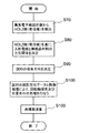
Hereinafter, a procedure for acquiring a scanning transmission electron microscope image and a converged electron beam diffraction image of the electron beam tomography method according to the embodiment of the present invention will be described with reference to FIG. FIG. 6 is a flowchart showing a procedure for acquiring a series of electron microscope images and electron beam scattered images in the electron beam tomography method according to the embodiment.
本実施形態の電子線トモグラフィ法では、様々な角度から撮影した走査透過電子顕微鏡像を取得する。この走査透過電子顕微鏡像の取得は図6に示すように行うことができる。 In the electron tomography method of this embodiment, scanning transmission electron microscope images taken from various angles are acquired. This scanning transmission electron microscope image can be obtained as shown in FIG.
まず、試料3を取り付けた試料ホルダ6を走査透過電子顕微鏡装置にセットし、走査透過電子顕微鏡の観察条件の設定及び光軸調整を行う(ステップS20)。
First, the
次に、評価部位3aの表面を収束した電子線で走査しながら、透過した電子線91を環状暗視野検出器22で検出することにより、走査透過電子顕微鏡像(STEM像)を取得する(ステップS30)。その後、試料ホルダ6を回転させずに、すなわち、試料3(評価部位3a及び単結晶部位3b)の角度を変えずに、収束させた電子線を単結晶部位3bの所定の箇所に一定時間照射して、透過した電子線92をCCDカメラ23で検出して単結晶部位3bの収束電子線回折(CBED)像を取得する(ステップS40)。
Next, a scanning transmission electron microscope image (STEM image) is obtained by detecting the transmitted
次に、試料ホルダ6を所定の角度(例えば1度)だけ回転させる(ステップS50)。そして、設定された角度範囲内での走査透過電子顕微鏡像及び収束電子線回折像の取得が完了しているか判断し(ステップS60)、完了していない場合には(NO)ステップS30に戻り、完了している場合には(YES)走査透過電子顕微鏡10による測定を終了する。
Next, the
以上の処理により、試料を様々な角度から投影した一連の走査透過電子顕微鏡像及び収束電子線回折像を取得できる。 Through the above processing, a series of scanning transmission electron microscope images and convergent electron beam diffraction images obtained by projecting the sample from various angles can be acquired.
(データ解析)
以下、図7及び図8を参照しつつ、本発明の実施形態に係る電子線トモグラフィ法の画像データの処理手順について説明する。ここに、図7は、実施形態に係る電子線トモグラフィ法のデータ解析手順を示すフロー図である。図8は、シリコン単結晶に収束電子線を照射したときに観察されるHOLZ線の角度依存性を計算により求めた結果を示す図である。
(Data analysis)
Hereinafter, the image data processing procedure of the electron beam tomography method according to the embodiment of the present invention will be described with reference to FIGS. 7 and 8. FIG. 7 is a flowchart showing a data analysis procedure of the electron beam tomography method according to the embodiment. FIG. 8 is a diagram showing the results of calculating the angular dependence of the HOLZ line observed when a focused electron beam is irradiated on a silicon single crystal.
本実施形態に係る画像データ処理は、図7に示すように、まず、取得した一連の収束電子線回折(CBED)像から、高次ラウエゾーン線(HOLZ線:High Order Laue Zone)を抽出する(ステップS70)。次に、検出されたHOLZ線を計算結果から求めたHOLZ線と対比して、その収束電子線回折像取得時の電子線の照射角を求める(ステップS80)。HOLZ線は、例えばSi単結晶の(110)面に垂直な方向を0度として、傾斜角を増大させながら収束電子線を照射すると、図8に示すような像を生じ、電子線の入射角に応じてその像が変化する。このHOLZ線の像を検出することにより、試料への電子線の入射角を少なくとも0.05度の精度で判別することができ、評価部位3aと電子線との角度を正確に決定することができる。これにより、評価部位3a上で電子線を走査して得られた走査透過電子顕微鏡像が、評価部位3aをどの角度から観察しているかといった、投影方向を厳密に決定することができる(ステップS90)。
In the image data processing according to the present embodiment, as shown in FIG. 7, first, a high-order Laue zone line (HOLZ line: High Order Laue Zone) is extracted from a series of acquired focused electron diffraction (CBED) images ( Step S70). Next, by comparing the detected HOLZ line with the HOLZ line obtained from the calculation result, the irradiation angle of the electron beam at the time of obtaining the converged electron beam diffraction image is obtained (step S80). When the HOLZ line is irradiated with a convergent electron beam while increasing the tilt angle with the direction perpendicular to the (110) plane of the Si single crystal being 0 degrees, for example, an image as shown in FIG. The image changes in response to. By detecting the image of the HOLZ line, the incident angle of the electron beam to the sample can be determined with an accuracy of at least 0.05 degrees, and the angle between the
次に、一連の走査透過電子顕微鏡像について、投影方向の情報と、画像処理を併用して、回転軸の探索及び位置合わせを行う(ステップS100)。回転軸の探索及び位置合わせの手法は、例えば以下の方法で行うことができる。 Next, for a series of scanning transmission electron microscope images, the information on the projection direction and image processing are used together to search and align the rotation axis (step S100). The method of searching and positioning the rotation axis can be performed by the following method, for example.
位置合わせは、まず0度の走査透過電子顕微鏡像を参照画像に用い、それとプラス方向又はマイナス方向の最初の(最も角度差の小さな)回転画像との間で画像相関処理を行う(非特許文献1参照)。この画像相関処理では、回転画像側を参照画像との角度差分だけ回転させた後、参照画像と回転画像との相関関数を求め、その相関関数が最大となるように回転画像側を並進移動させる。次に、この位置合わせができた回転画像を参照画像に用い、最も角度差の小さな別の回転画像との間で画像相関処理を行う。このようにして一連の走査透過電子顕微鏡像の全てについて位置合わせを行うことができる。従来の画像相関法では、角度ズレ量を変数として相関関数を計算していたが、本実施形態の電子線トモグラフィ法によれば、試料3の傾斜角度及び角度ズレを測定により求めた値に固定して相関関数を計算することができるため、位置合わせの精度が向上する。
For alignment, first, a scanning transmission electron microscope image of 0 degrees is used as a reference image, and image correlation processing is performed between the image and the first (smallest angle difference) rotated image in the plus or minus direction (non-patent document). 1). In this image correlation process, the rotated image side is rotated by an angle difference from the reference image, and then a correlation function between the reference image and the rotated image is obtained, and the rotated image side is translated so that the correlation function is maximized. . Next, the rotated image that has been aligned is used as a reference image, and image correlation processing is performed with another rotated image having the smallest angular difference. In this way, alignment can be performed for all of the series of scanning transmission electron microscope images. In the conventional image correlation method, the correlation function is calculated by using the amount of angle deviation as a variable. However, according to the electron beam tomography method of the present embodiment, the inclination angle and the angle deviation of the
回転軸の決定は、まず、各投影方向の走査透過電子顕微鏡像から複数の特徴点を自動的に検出する。次に、この特徴点にステレオ視差測定法を適用することにより、各対応点の3次元座標を求める。そして対応点の軌跡を求め、この軌跡の誤差が最小の点として求めることができる(非特許文献1参照)。上述のように本実施形態の電子線トモグラフィ法によれば、試料3の傾斜角度が正確に求まるため、ステレオ視差測定法で求めた各対応点の3次元座標を正確に求めることができ、より高精度に回転軸を求めることができる。
In determining the rotation axis, first, a plurality of feature points are automatically detected from a scanning transmission electron microscope image in each projection direction. Next, a three-dimensional coordinate of each corresponding point is obtained by applying a stereo parallax measurement method to this feature point. Then, the locus of the corresponding point can be obtained, and the locus error can be obtained as the minimum point (see Non-Patent Document 1). As described above, according to the electron tomography method of the present embodiment, since the inclination angle of the
最後に、位置合わせされた一連の走査透過電子顕微鏡像及び回転軸及び投影方向の情報に基づいて評価部位3aの立体構造の再構築演算を行う(ステップS110)。尚、再構築演算については、非特許文献1や特許文献1等に記載された手法で行うことができる。
Finally, a reconstruction calculation of the three-dimensional structure of the
尚、本実施形態は上述の例に限られず、収束電子線回折像から菊池線を抽出して菊池線のパターンを用いて単結晶部位3bへの電子線の照射角を求めるようにしてもよい。ここに、図9はシリコン単結晶に収束電子線を照射したときに観察される菊池線の角度依存性を計算により求めた結果を示す図である。単結晶部位3bとしてのシリコン単結晶の(110)面に垂直な方向を0度とし、傾斜角を増大させながら収束電子線を照射したときに観測される菊池線は、図9に示すような像を生じ、電子線の入射角に応じてその像が変化する。これにより、単結晶部位3bへの収束電子線回折像から得られる菊池線のパターンを検出することによっても少なくとも0.05度程度の精度で単結晶部位3bへの電子線の照射角度、すなわち、評価部位3aの投影方向を決定することができる。
Note that the present embodiment is not limited to the above example, and an irradiation angle of the electron beam to the
以上のように本実施形態の電子線トモグラフィ法によれば、評価部位3aに固定された単結晶部位3bの収束電子線回折像からHOLZ線又は菊池線を検出してこれに基づいて、評価部位3aの走査電子顕微鏡像の投影方向を正確に(少なくとも0.05度精度で)決定することができる。また、試料3が支持膜5に傾いて固定されてしまった場合や、回転軸が試料3の内部に存在せずに偏心している場合(試料3がきれいに回転していない場合)でも収束電子線回折像を用いて正確な投影方向を得ることができるため、その透過電子顕微鏡画像を立体構造の解析に利用することができる。
As described above, according to the electron tomography method of the present embodiment, the HOLZ line or the Kikuchi line is detected from the converged electron beam diffraction image of the
したがって、試料傾斜角度の決定、位置合わせ、回転軸の決定をより正確に行うことができ、再構築演算の精度が向上し、より精度の高い立体像を得ることができる。 Therefore, determination of the sample tilt angle, alignment, and determination of the rotation axis can be performed more accurately, the accuracy of the reconstruction calculation can be improved, and a more accurate stereoscopic image can be obtained.
(その他の実施形態)
上記の実施形態では、評価部位3a及び単結晶部位3bを1軸周りに回転させて、走査電子顕微鏡像及び収束電子線回折像を取得していたが、本発明はこれに限定されるものではなく、試料を2軸又は3軸周りに回転させて走査電子顕微鏡像及び収束電子線回折像を取得する構成としてもよい。これにより、走査透過電子顕微鏡像を取得できる角度領域が増大し、情報欠落領域を減少させることができる。
(Other embodiments)
In the above embodiment, the
また、上記実施形態の走査電子顕微鏡装置11では、評価部位3aに収束した電子線を照射して透過した電子を環状暗視野検出器によって検出する構成としていたが、これ以外にも、評価部位3a全体に同時に電子線を照射して透過電子顕微鏡像をCCDカメラ等で取得するように構成して透過電子顕微鏡像を得る構成としてもよい。
Moreover, in the scanning
また、上記実施形態では試料3と電子線の照射角を決定するために、単結晶部位3bの収束電子線回折像を用いていたが、これに変えて、単結晶部位3bに収束していない電子線を照射して得られる、スポット状の通常の電子線回折像を用いて電子線の照射角を決定する構成としてもよい。この場合には、収束電子線回折像を用いて決定する場合よりも角度精度が低下するが、試料3の投影方向を画像処理を行わずに決定することができる。
Moreover, in the said embodiment, in order to determine the irradiation angle of the
3…試料、3a…評価部位、3b…単結晶、5…支持膜、5a…断面、6…試料ホルダ、6a…窓部、10…電子線トモグラフィ装置、11…走査透過電子顕微鏡、12…制御装置、13…解析装置、15…電子銃、17…収束レンズ、18…収束レンズ、19…収束レンズ絞り、20…走査コイル、21…対物レンズ、22…環状暗視野検出器、23…CCDカメラ、90…電子ビーム、91…透過電子線、92…回折電子線。
DESCRIPTION OF
Claims (6)
前記評価部位に前記電子線を照射して透過電子顕微鏡像を取得すると共に前記電子線の照射角度を変化させずに前記単結晶部位に前記電子線を照射して電子線回折像を取得する操作をそれぞれの角度毎に行うことにより、一連の前記透過電子顕微鏡像及び前記電子線回折像を取得する工程と、
前記電子線回折像から前記試料への前記電子線の入射方位を求めて前記透過電子顕微鏡像の各々についての投影方向を決定する工程と、
前記透過電子顕微鏡像の各々についての投影方向の情報を用いて、一連の前記透過電子顕微鏡像の位置合わせを行い、前記評価部位の立体構造を再構築する工程と、
を有することを特徴とする電子線トモグラフィ法。 A sample having an evaluation site whose structure is to be evaluated and a single crystal site integrally bonded to the evaluation site is irradiated with an electron beam from a plurality of angles to obtain a series of transmission electron beam images. An electron tomography method for reconstructing the three-dimensional structure of the evaluation site based on an image,
An operation of acquiring a transmission electron microscope image by irradiating the evaluation site with the electron beam and acquiring an electron beam diffraction image by irradiating the single crystal site with the electron beam without changing the irradiation angle of the electron beam. To obtain a series of the transmission electron microscopic image and the electron diffraction image by performing each for each angle;
Determining the incident direction of the electron beam to the sample from the electron diffraction image and determining the projection direction for each of the transmission electron microscope images;
Using the information of the projection direction for each of the transmission electron microscope images, aligning the series of transmission electron microscope images, and reconstructing the three-dimensional structure of the evaluation site;
An electron beam tomography method characterized by comprising:
前記試料を保持すると共に、前記試料を少なくとも1軸周りに回転させて前記試料への前記電子線の照射角度を変化させることができる試料保持部材と、
前記試料からの透過電子顕微鏡像及び電子線回折像を検出する検出器と、
前記電子線照射装置、前記試料保持部材、及び前記検出器を制御して、前記評価部位に前記電子線を照射して透過電子顕微鏡像を取得すると共に前記電子線の照射角度を変化させずに前記単結晶部位に前記電子線を照射して電子線回折像を取得する操作を複数の角度で行うことにより、一連の透過電子顕微鏡像及び一連の電子線回折像を取得し、前記電子線回折像から前記透過電子顕微鏡像の各々についての投影方向を決定し、その投影方向の情報を用いて前記一連の透過電子顕微鏡像の位置合わせを行い前記評価部位の立体構造を再構築する制御装置と、
を備えたことを特徴とする電子線トモグラフィ装置。 An electron beam irradiation apparatus for irradiating an electron beam to a sample having an evaluation site whose structure is to be evaluated and a single crystal site integrally bonded to the evaluation site;
A sample holding member capable of holding the sample and changing the irradiation angle of the electron beam to the sample by rotating the sample around at least one axis;
A detector for detecting a transmission electron microscope image and an electron diffraction image from the sample;
Controlling the electron beam irradiation device, the sample holding member, and the detector to irradiate the electron beam onto the evaluation site to obtain a transmission electron microscope image and without changing the irradiation angle of the electron beam A series of transmission electron microscope images and a series of electron beam diffraction images are obtained by performing the operation of irradiating the single crystal part with the electron beam to obtain an electron beam diffraction image at a plurality of angles, and the electron beam diffraction is obtained. A control device that determines a projection direction for each of the transmission electron microscope images from the image, aligns the series of transmission electron microscope images using information on the projection direction, and reconstructs the three-dimensional structure of the evaluation site; ,
An electron beam tomography apparatus comprising:
Priority Applications (1)
| Application Number | Priority Date | Filing Date | Title |
|---|---|---|---|
| JP2007330320A JP5309552B2 (en) | 2007-12-21 | 2007-12-21 | Electron beam tomography method and electron beam tomography apparatus |
Applications Claiming Priority (1)
| Application Number | Priority Date | Filing Date | Title |
|---|---|---|---|
| JP2007330320A JP5309552B2 (en) | 2007-12-21 | 2007-12-21 | Electron beam tomography method and electron beam tomography apparatus |
Publications (2)
| Publication Number | Publication Date |
|---|---|
| JP2009152120A JP2009152120A (en) | 2009-07-09 |
| JP5309552B2 true JP5309552B2 (en) | 2013-10-09 |
Family
ID=40921008
Family Applications (1)
| Application Number | Title | Priority Date | Filing Date |
|---|---|---|---|
| JP2007330320A Expired - Fee Related JP5309552B2 (en) | 2007-12-21 | 2007-12-21 | Electron beam tomography method and electron beam tomography apparatus |
Country Status (1)
| Country | Link |
|---|---|
| JP (1) | JP5309552B2 (en) |
Cited By (1)
| Publication number | Priority date | Publication date | Assignee | Title |
|---|---|---|---|---|
| WO2015072609A1 (en) * | 2013-11-18 | 2015-05-21 | 한국지질자원연구원 | Three-dimensional measuring method for porous geopolymer using electronic tomography |
Families Citing this family (10)
| Publication number | Priority date | Publication date | Assignee | Title |
|---|---|---|---|---|
| JP5339368B2 (en) * | 2009-09-18 | 2013-11-13 | 独立行政法人産業技術総合研究所 | 3D image construction image processing method in electron microscope |
| JP5670096B2 (en) * | 2009-11-17 | 2015-02-18 | 日本電子株式会社 | Method and apparatus for acquiring three-dimensional image of sample using tomography method |
| JP5292326B2 (en) * | 2010-01-29 | 2013-09-18 | 株式会社日立ハイテクノロジーズ | Standard sample preparation method and standard sample |
| JP5321918B2 (en) * | 2010-06-15 | 2013-10-23 | 独立行政法人産業技術総合研究所 | Sample preparation method for electron microscope |
| JP5331780B2 (en) * | 2010-11-30 | 2013-10-30 | 株式会社日立ハイテクノロジーズ | Electron microscope, image reconstruction system for electron microscope, and image reconstruction method for electron microscope |
| JP2014082134A (en) * | 2012-10-17 | 2014-05-08 | Fujitsu Ltd | Electronic device and method for irradiating electron beam |
| KR101543417B1 (en) | 2013-11-29 | 2015-08-10 | 한국해양과학기술원 | Improvement Method of Image Alignment Accuracy in Electron-Tomography |
| JP5703404B2 (en) * | 2014-03-07 | 2015-04-22 | 株式会社日立ハイテクノロジーズ | Charged particle beam apparatus and length measuring method using charged particle beam |
| KR102724079B1 (en) | 2019-05-20 | 2024-10-29 | 엘디코 사이언티픽 아게 | Diffractometer for charged particle crystallography |
| JP7693426B2 (en) * | 2021-07-12 | 2025-06-17 | キオクシア株式会社 | Analysis method |
Family Cites Families (7)
| Publication number | Priority date | Publication date | Assignee | Title |
|---|---|---|---|---|
| JPH03246861A (en) * | 1990-02-23 | 1991-11-05 | Nec Corp | Permeation type electron microscope |
| JP3422045B2 (en) * | 1993-06-21 | 2003-06-30 | 株式会社日立製作所 | Electron microscope for measuring composition and lattice strain and its observation method |
| JP3304681B2 (en) * | 1995-04-25 | 2002-07-22 | 株式会社日立製作所 | Electron microscope and three-dimensional atomic array observation method |
| JPH09213253A (en) * | 1996-01-31 | 1997-08-15 | Ricoh Co Ltd | Method of structural analysis of amorphous materials by electron diffraction |
| JPH10214587A (en) * | 1997-01-30 | 1998-08-11 | Hitachi Ltd | Scanning transmission electron microscope for stereoscopic observation and stereoscopic image forming system |
| JP3984521B2 (en) * | 2002-09-20 | 2007-10-03 | 松下電器産業株式会社 | Observation method using a transmission electron microscope |
| JP2005019218A (en) * | 2003-06-26 | 2005-01-20 | Jeol Ltd | Electron microscope equipment |
-
2007
- 2007-12-21 JP JP2007330320A patent/JP5309552B2/en not_active Expired - Fee Related
Cited By (1)
| Publication number | Priority date | Publication date | Assignee | Title |
|---|---|---|---|---|
| WO2015072609A1 (en) * | 2013-11-18 | 2015-05-21 | 한국지질자원연구원 | Three-dimensional measuring method for porous geopolymer using electronic tomography |
Also Published As
| Publication number | Publication date |
|---|---|
| JP2009152120A (en) | 2009-07-09 |
Similar Documents
| Publication | Publication Date | Title |
|---|---|---|
| JP5309552B2 (en) | Electron beam tomography method and electron beam tomography apparatus | |
| US7863564B2 (en) | Electric charged particle beam microscope and microscopy | |
| US9202671B2 (en) | Charged particle beam apparatus and sample processing method using charged particle beam apparatus | |
| JP5296413B2 (en) | Cross-sectional image acquisition method using composite charged particle beam apparatus and composite charged particle beam apparatus | |
| CN106370680B (en) | It is acquired for TEM/STEM tomography tilt series and reference of reference is formed | |
| JP2003014667A (en) | Observation apparatus and observation method using electron beam | |
| US20070023651A1 (en) | Methods for sample preparation and observation, charged particle apparatus | |
| JP2008270056A (en) | Scanning transmission electron microscope | |
| JP2012013703A (en) | Method for electron diffraction tomography | |
| US12362135B2 (en) | Method and system for automatic zone axis alignment | |
| EP4067886A1 (en) | Method and system to determine crystal structure | |
| WO2017104186A1 (en) | Ebsd detecting device | |
| US10541108B2 (en) | Method and apparatus for transmission electron microscopy | |
| JP3304681B2 (en) | Electron microscope and three-dimensional atomic array observation method | |
| JP7527282B2 (en) | Electron diffraction imaging system for determining molecular structure and conformation | |
| JP2011204367A (en) | Sample stand for electron microscope | |
| US20230377836A1 (en) | Analysis System | |
| CN208420756U (en) | A kind of imaging system | |
| JP7304098B2 (en) | 3D image observation method and sample grid used therefor | |
| JP2022155554A (en) | Method and system for acquiring three dimensional electron diffraction data | |
| JP4845452B2 (en) | Sample observation method and charged particle beam apparatus | |
| JP2021043073A (en) | Error calculation device, charged particle beam device, error calculation method and program | |
| WO2019038917A1 (en) | Correction sample, and electron beam adjustment method and electron beam device using same | |
| JP2003317654A (en) | Electron microscopy method, electron microscope and biological sample inspection method and biological inspection apparatus using the same | |
| JP2653084B2 (en) | Surface analyzer |
Legal Events
| Date | Code | Title | Description |
|---|---|---|---|
| A621 | Written request for application examination |
Free format text: JAPANESE INTERMEDIATE CODE: A621 Effective date: 20100820 |
|
| A977 | Report on retrieval |
Free format text: JAPANESE INTERMEDIATE CODE: A971007 Effective date: 20120620 |
|
| A131 | Notification of reasons for refusal |
Free format text: JAPANESE INTERMEDIATE CODE: A131 Effective date: 20120626 |
|
| A131 | Notification of reasons for refusal |
Free format text: JAPANESE INTERMEDIATE CODE: A131 Effective date: 20130122 |
|
| A521 | Request for written amendment filed |
Free format text: JAPANESE INTERMEDIATE CODE: A523 Effective date: 20130215 |
|
| TRDD | Decision of grant or rejection written | ||
| A01 | Written decision to grant a patent or to grant a registration (utility model) |
Free format text: JAPANESE INTERMEDIATE CODE: A01 Effective date: 20130604 |
|
| A61 | First payment of annual fees (during grant procedure) |
Free format text: JAPANESE INTERMEDIATE CODE: A61 Effective date: 20130617 |
|
| R150 | Certificate of patent or registration of utility model |
Free format text: JAPANESE INTERMEDIATE CODE: R150 |
|
| LAPS | Cancellation because of no payment of annual fees |