JP5301895B2 - Liquid crystal display - Google Patents
Liquid crystal display Download PDFInfo
- Publication number
- JP5301895B2 JP5301895B2 JP2008171954A JP2008171954A JP5301895B2 JP 5301895 B2 JP5301895 B2 JP 5301895B2 JP 2008171954 A JP2008171954 A JP 2008171954A JP 2008171954 A JP2008171954 A JP 2008171954A JP 5301895 B2 JP5301895 B2 JP 5301895B2
- Authority
- JP
- Japan
- Prior art keywords
- pixel
- liquid crystal
- subpixel
- blue
- width
- Prior art date
- Legal status (The legal status is an assumption and is not a legal conclusion. Google has not performed a legal analysis and makes no representation as to the accuracy of the status listed.)
- Active
Links
Images

Classifications
-
- G—PHYSICS
- G02—OPTICS
- G02F—OPTICAL DEVICES OR ARRANGEMENTS FOR THE CONTROL OF LIGHT BY MODIFICATION OF THE OPTICAL PROPERTIES OF THE MEDIA OF THE ELEMENTS INVOLVED THEREIN; NON-LINEAR OPTICS; FREQUENCY-CHANGING OF LIGHT; OPTICAL LOGIC ELEMENTS; OPTICAL ANALOGUE/DIGITAL CONVERTERS
- G02F1/00—Devices or arrangements for the control of the intensity, colour, phase, polarisation or direction of light arriving from an independent light source, e.g. switching, gating or modulating; Non-linear optics
- G02F1/01—Devices or arrangements for the control of the intensity, colour, phase, polarisation or direction of light arriving from an independent light source, e.g. switching, gating or modulating; Non-linear optics for the control of the intensity, phase, polarisation or colour
- G02F1/13—Devices or arrangements for the control of the intensity, colour, phase, polarisation or direction of light arriving from an independent light source, e.g. switching, gating or modulating; Non-linear optics for the control of the intensity, phase, polarisation or colour based on liquid crystals, e.g. single liquid crystal display cells
- G02F1/133—Constructional arrangements; Operation of liquid crystal cells; Circuit arrangements
- G02F1/1333—Constructional arrangements; Manufacturing methods
- G02F1/1335—Structural association of cells with optical devices, e.g. polarisers or reflectors
- G02F1/133509—Filters, e.g. light shielding masks
- G02F1/133512—Light shielding layers, e.g. black matrix
-
- G—PHYSICS
- G02—OPTICS
- G02F—OPTICAL DEVICES OR ARRANGEMENTS FOR THE CONTROL OF LIGHT BY MODIFICATION OF THE OPTICAL PROPERTIES OF THE MEDIA OF THE ELEMENTS INVOLVED THEREIN; NON-LINEAR OPTICS; FREQUENCY-CHANGING OF LIGHT; OPTICAL LOGIC ELEMENTS; OPTICAL ANALOGUE/DIGITAL CONVERTERS
- G02F1/00—Devices or arrangements for the control of the intensity, colour, phase, polarisation or direction of light arriving from an independent light source, e.g. switching, gating or modulating; Non-linear optics
- G02F1/01—Devices or arrangements for the control of the intensity, colour, phase, polarisation or direction of light arriving from an independent light source, e.g. switching, gating or modulating; Non-linear optics for the control of the intensity, phase, polarisation or colour
- G02F1/13—Devices or arrangements for the control of the intensity, colour, phase, polarisation or direction of light arriving from an independent light source, e.g. switching, gating or modulating; Non-linear optics for the control of the intensity, phase, polarisation or colour based on liquid crystals, e.g. single liquid crystal display cells
- G02F1/133—Constructional arrangements; Operation of liquid crystal cells; Circuit arrangements
- G02F1/1333—Constructional arrangements; Manufacturing methods
- G02F1/1335—Structural association of cells with optical devices, e.g. polarisers or reflectors
- G02F1/133509—Filters, e.g. light shielding masks
- G02F1/133514—Colour filters
-
- G—PHYSICS
- G02—OPTICS
- G02F—OPTICAL DEVICES OR ARRANGEMENTS FOR THE CONTROL OF LIGHT BY MODIFICATION OF THE OPTICAL PROPERTIES OF THE MEDIA OF THE ELEMENTS INVOLVED THEREIN; NON-LINEAR OPTICS; FREQUENCY-CHANGING OF LIGHT; OPTICAL LOGIC ELEMENTS; OPTICAL ANALOGUE/DIGITAL CONVERTERS
- G02F1/00—Devices or arrangements for the control of the intensity, colour, phase, polarisation or direction of light arriving from an independent light source, e.g. switching, gating or modulating; Non-linear optics
- G02F1/01—Devices or arrangements for the control of the intensity, colour, phase, polarisation or direction of light arriving from an independent light source, e.g. switching, gating or modulating; Non-linear optics for the control of the intensity, phase, polarisation or colour
- G02F1/13—Devices or arrangements for the control of the intensity, colour, phase, polarisation or direction of light arriving from an independent light source, e.g. switching, gating or modulating; Non-linear optics for the control of the intensity, phase, polarisation or colour based on liquid crystals, e.g. single liquid crystal display cells
- G02F1/133—Constructional arrangements; Operation of liquid crystal cells; Circuit arrangements
- G02F1/136—Liquid crystal cells structurally associated with a semi-conducting layer or substrate, e.g. cells forming part of an integrated circuit
- G02F1/1362—Active matrix addressed cells
- G02F1/136286—Wiring, e.g. gate line, drain line
-
- G—PHYSICS
- G02—OPTICS
- G02F—OPTICAL DEVICES OR ARRANGEMENTS FOR THE CONTROL OF LIGHT BY MODIFICATION OF THE OPTICAL PROPERTIES OF THE MEDIA OF THE ELEMENTS INVOLVED THEREIN; NON-LINEAR OPTICS; FREQUENCY-CHANGING OF LIGHT; OPTICAL LOGIC ELEMENTS; OPTICAL ANALOGUE/DIGITAL CONVERTERS
- G02F1/00—Devices or arrangements for the control of the intensity, colour, phase, polarisation or direction of light arriving from an independent light source, e.g. switching, gating or modulating; Non-linear optics
- G02F1/01—Devices or arrangements for the control of the intensity, colour, phase, polarisation or direction of light arriving from an independent light source, e.g. switching, gating or modulating; Non-linear optics for the control of the intensity, phase, polarisation or colour
- G02F1/13—Devices or arrangements for the control of the intensity, colour, phase, polarisation or direction of light arriving from an independent light source, e.g. switching, gating or modulating; Non-linear optics for the control of the intensity, phase, polarisation or colour based on liquid crystals, e.g. single liquid crystal display cells
- G02F1/133—Constructional arrangements; Operation of liquid crystal cells; Circuit arrangements
- G02F1/136—Liquid crystal cells structurally associated with a semi-conducting layer or substrate, e.g. cells forming part of an integrated circuit
- G02F1/1362—Active matrix addressed cells
- G02F1/1368—Active matrix addressed cells in which the switching element is a three-electrode device
-
- G—PHYSICS
- G02—OPTICS
- G02F—OPTICAL DEVICES OR ARRANGEMENTS FOR THE CONTROL OF LIGHT BY MODIFICATION OF THE OPTICAL PROPERTIES OF THE MEDIA OF THE ELEMENTS INVOLVED THEREIN; NON-LINEAR OPTICS; FREQUENCY-CHANGING OF LIGHT; OPTICAL LOGIC ELEMENTS; OPTICAL ANALOGUE/DIGITAL CONVERTERS
- G02F1/00—Devices or arrangements for the control of the intensity, colour, phase, polarisation or direction of light arriving from an independent light source, e.g. switching, gating or modulating; Non-linear optics
- G02F1/01—Devices or arrangements for the control of the intensity, colour, phase, polarisation or direction of light arriving from an independent light source, e.g. switching, gating or modulating; Non-linear optics for the control of the intensity, phase, polarisation or colour
- G02F1/13—Devices or arrangements for the control of the intensity, colour, phase, polarisation or direction of light arriving from an independent light source, e.g. switching, gating or modulating; Non-linear optics for the control of the intensity, phase, polarisation or colour based on liquid crystals, e.g. single liquid crystal display cells
- G02F1/133—Constructional arrangements; Operation of liquid crystal cells; Circuit arrangements
- G02F1/1333—Constructional arrangements; Manufacturing methods
- G02F1/1343—Electrodes
- G02F1/134309—Electrodes characterised by their geometrical arrangement
- G02F1/134363—Electrodes characterised by their geometrical arrangement for applying an electric field parallel to the substrate, i.e. in-plane switching [IPS]
-
- G—PHYSICS
- G02—OPTICS
- G02F—OPTICAL DEVICES OR ARRANGEMENTS FOR THE CONTROL OF LIGHT BY MODIFICATION OF THE OPTICAL PROPERTIES OF THE MEDIA OF THE ELEMENTS INVOLVED THEREIN; NON-LINEAR OPTICS; FREQUENCY-CHANGING OF LIGHT; OPTICAL LOGIC ELEMENTS; OPTICAL ANALOGUE/DIGITAL CONVERTERS
- G02F2201/00—Constructional arrangements not provided for in groups G02F1/00 - G02F7/00
- G02F2201/12—Constructional arrangements not provided for in groups G02F1/00 - G02F7/00 electrode
- G02F2201/121—Constructional arrangements not provided for in groups G02F1/00 - G02F7/00 electrode common or background
-
- G—PHYSICS
- G02—OPTICS
- G02F—OPTICAL DEVICES OR ARRANGEMENTS FOR THE CONTROL OF LIGHT BY MODIFICATION OF THE OPTICAL PROPERTIES OF THE MEDIA OF THE ELEMENTS INVOLVED THEREIN; NON-LINEAR OPTICS; FREQUENCY-CHANGING OF LIGHT; OPTICAL LOGIC ELEMENTS; OPTICAL ANALOGUE/DIGITAL CONVERTERS
- G02F2201/00—Constructional arrangements not provided for in groups G02F1/00 - G02F7/00
- G02F2201/12—Constructional arrangements not provided for in groups G02F1/00 - G02F7/00 electrode
- G02F2201/123—Constructional arrangements not provided for in groups G02F1/00 - G02F7/00 electrode pixel
-
- G—PHYSICS
- G02—OPTICS
- G02F—OPTICAL DEVICES OR ARRANGEMENTS FOR THE CONTROL OF LIGHT BY MODIFICATION OF THE OPTICAL PROPERTIES OF THE MEDIA OF THE ELEMENTS INVOLVED THEREIN; NON-LINEAR OPTICS; FREQUENCY-CHANGING OF LIGHT; OPTICAL LOGIC ELEMENTS; OPTICAL ANALOGUE/DIGITAL CONVERTERS
- G02F2201/00—Constructional arrangements not provided for in groups G02F1/00 - G02F7/00
- G02F2201/52—RGB geometrical arrangements
-
- G—PHYSICS
- G09—EDUCATION; CRYPTOGRAPHY; DISPLAY; ADVERTISING; SEALS
- G09G—ARRANGEMENTS OR CIRCUITS FOR CONTROL OF INDICATING DEVICES USING STATIC MEANS TO PRESENT VARIABLE INFORMATION
- G09G2300/00—Aspects of the constitution of display devices
- G09G2300/04—Structural and physical details of display devices
- G09G2300/0421—Structural details of the set of electrodes
- G09G2300/0434—Flat panel display in which a field is applied parallel to the display plane
-
- G—PHYSICS
- G09—EDUCATION; CRYPTOGRAPHY; DISPLAY; ADVERTISING; SEALS
- G09G—ARRANGEMENTS OR CIRCUITS FOR CONTROL OF INDICATING DEVICES USING STATIC MEANS TO PRESENT VARIABLE INFORMATION
- G09G2300/00—Aspects of the constitution of display devices
- G09G2300/04—Structural and physical details of display devices
- G09G2300/0439—Pixel structures
- G09G2300/0465—Improved aperture ratio, e.g. by size reduction of the pixel circuit, e.g. for improving the pixel density or the maximum displayable luminance or brightness
Description
本発明は液晶表示装置に係り、特に、カラー表示がなされる液晶表示装置に関する。 The present invention relates to a liquid crystal display device, and more particularly to a liquid crystal display device that performs color display.
カラー表示がなされる液晶表示装置は、隣接された3色以上の単位色画素によりカラー表示用の単位画素を構成するようになっている。 In a liquid crystal display device that performs color display, unit pixels for color display are configured by unit color pixels of three or more adjacent colors.
各単位色画素には、各単位色画素に応じた着色層(カラーフィルタ)を備え、これら着色層を通した光の混合によって観察者は所定の色を感知できるようになっている。 Each unit color pixel is provided with a colored layer (color filter) corresponding to each unit color pixel, and an observer can sense a predetermined color by mixing light passing through these colored layers.
そして、カラー表示用の単位画素において、単色表示させようとする場合は、当該色の単位色画素の液晶をONさせるとともに、他の色の単位色画素の液晶をOFFさせることによって実現している。 When the unit pixel for color display is to be displayed in a single color, it is realized by turning on the liquid crystal of the unit color pixel of that color and turning off the liquid crystal of the unit color pixel of the other color. .
そして、このような単色表示の場合において、表示面を斜め方向から観た場合、液晶がONしている単位色画素に隣接する他の単位色画素であって、観察者に近い側の画素(液晶はOFFとなっている)の色が混ざって見える(この明細書において混色と表現する)不都合が生じる。この理由は、たとえばバックライトからの光において、液晶がONしている単位色画素と、この単位色画素と隣接する他の単位画素を通る光路が存在するからである。 In such a monochromatic display, when the display surface is viewed from an oblique direction, other unit color pixels adjacent to the unit color pixel in which the liquid crystal is turned on and closer to the observer ( The color of the liquid crystal is OFF) appears to be mixed (expressed as mixed color in this specification). This is because, for example, in the light from the backlight, there is an optical path that passes through the unit color pixel in which the liquid crystal is ON and another unit pixel adjacent to the unit color pixel.
生産上のばらつきにより、液晶を狭持する対向配置された基板が、異なる色の単位画素が並ぶ方向にずれて固定された液晶表示装置の場合、単色表示において、液晶がONしている単位色画素に隣接する他の単位色画素の着色層が、液晶がONしている領域に近づいているまたは重なっているため、前記隣接する単位画素側の斜め方向から観察した場合、混色の不都合が特に顕著になる。この理由は、液晶がONしている領域に着色層が近づいているまたは重なっていることにより、前記光路の幅が広がるためである。 In the case of a liquid crystal display device in which the substrates arranged opposite to each other with the liquid crystal sandwiched due to production variations are fixed in a direction in which unit pixels of different colors are arranged, the unit color in which the liquid crystal is turned on in the single color display Since the colored layer of the other unit color pixel adjacent to the pixel approaches or overlaps the area where the liquid crystal is ON, there is a particular problem of color mixing when observed from an oblique direction on the adjacent unit pixel side. Become prominent. This is because the width of the optical path is widened when the colored layer approaches or overlaps the region where the liquid crystal is ON.
近年にあって、いわゆる広視野角に優れた液晶表示装置が開発され、斜め方向からの観察の機会が多くなり、前記混色による画質劣化が認識されやすくなっている。 In recent years, a liquid crystal display device having a so-called wide viewing angle has been developed, and an opportunity for observation from an oblique direction is increased, and image quality deterioration due to the color mixture is easily recognized.
このため、従来では、各単位色画素の間に配置させる遮光層(ブラックマトリックス)の幅を一律に太くすることで、前記混色による弊害を回避させていた。すなわち、液晶がONしている単位色画素に隣接する他の単位色画素のカラーフィルタを通過する光を、幅の太いブラックマトリックスで遮ることで、前記混色の回避を対策するようにしたものである。 For this reason, conventionally, the width of the light shielding layer (black matrix) disposed between the unit color pixels is uniformly increased to avoid the adverse effects caused by the color mixture. That is, light that passes through the color filter of another unit color pixel adjacent to the unit color pixel in which the liquid crystal is ON is blocked by a thick black matrix to prevent the color mixture. is there.
なお、本願に関連する文献として、下記特許文献1、あるいは特許文献2がある。
しかし、上述したように各単位色画素の間に配置させるブラックマトリックスの幅を一律に太くした場合、該ブラックマトリックスの形成領域を除く実質的な画素の領域が狭まり、いわゆる画素の開口率が低下してしまう不都合が生じる。 However, when the width of the black matrix arranged between the unit color pixels is uniformly increased as described above, the substantial pixel area excluding the black matrix forming area is narrowed, and so-called pixel aperture ratio is reduced. This causes inconvenience.
このことは、液晶表示装置としての輝度の低下をもたらし、この不都合を回避させることが要望されるに至る。 This leads to a decrease in luminance as a liquid crystal display device, and it is desired to avoid this inconvenience.
本発明の目的は、画素の開口率の向上を図りつつ、表示面を斜め方向から見た場合に色の混色を回避させることのできる液晶表示装置を提供することにある。 An object of the present invention is to provide a liquid crystal display device capable of avoiding color mixture when the display surface is viewed obliquely while improving the aperture ratio of pixels.
液晶表示装置は、液晶を透過する光の効率(透過効率)が大きく、液晶のON時とOFF時の透過効率比(透過コントラスト比)が高くなるように液晶のリターデーションが設定されている。この場合、液晶のON時とOFF時の透過効率比が高くなるように液晶のリターデーションを設定すると、液晶を通過した光は光源よりも黄色味を帯びる性質を有する。 In the liquid crystal display device, the retardation of the liquid crystal is set so that the efficiency of light passing through the liquid crystal (transmission efficiency) is high and the transmission efficiency ratio (transmission contrast ratio) when the liquid crystal is on and off is high. In this case, when the retardation of the liquid crystal is set so that the transmission efficiency ratio when the liquid crystal is on and off is high, the light passing through the liquid crystal has a property of being more yellowish than the light source.
このため、表示の黄色味を回避するため、光源として黄色の補色である青色味を帯びたものを使用する方法が考えられる。 For this reason, in order to avoid the yellowishness of the display, a method of using a blueishness which is a complementary color of yellow as the light source can be considered.
このように青色味を帯びた光源を使用した液晶表示装置の場合、単色表示において斜め方向からパネルを観察すると、青色が混ざって生じる混色がより視認されやすくなる。 In the case of a liquid crystal display device using a light source with a blue tint as described above, when a panel is observed from an oblique direction in monochromatic display, a mixed color generated by mixing blue becomes more visible.
つまり、赤の単色表示において、隣接する青色画素側の斜め方向から観察した場合、光源が青色味を帯びていることにより青色が混ざって生じる混色が強調されるため、混色の不都合が顕著になる。一方、赤の単色表示において、隣接する緑色画素側の斜め方向から観察した場合、緑色が混ざって生じる混色の不都合は、青色が混ざって生じる混色の不都合と比較して視認しづらくなる。 In other words, in a single color display of red, when observed from an oblique direction on the side of the adjacent blue pixel, since the light source is tinged with blue, the color mixture generated by mixing blue is emphasized, and thus the inconvenience of color mixing becomes significant. . On the other hand, in red single color display, when observed from an oblique direction on the side of an adjacent green pixel, the inconvenience of color mixing caused by mixing green becomes difficult to visually recognize compared to the inconvenience of color mixing caused by mixing blue.
このことから、赤色画素と青色画素の間のブラックマトリックスの幅を太くするが、赤色画素と緑色画素の間のブラックマトリックスの幅は太くする必要がなくなることが判る。したがって、ブラックマトリックスの幅を一律に太くする場合と比較し、画素の開口率を向上させることができる。 From this, it can be seen that the width of the black matrix between the red pixel and the blue pixel is increased, but it is not necessary to increase the width of the black matrix between the red pixel and the green pixel. Therefore, the aperture ratio of the pixels can be improved as compared with the case where the width of the black matrix is uniformly increased.
また、この場合において、赤色画素と青色画素の間のブラックマトリックスを青色画素の中心側へずらして配置させることによって、当該ブラックマトリックスの幅を大きくする必要をなくすことができる。上述のように赤色画素と青色画素の間のブラックマトリックスを青色画素の中心側へずらすことによって、赤の単色表示の際の隣接する青色画素側の斜め方向からの観察において、青色の光を前記ブラックマトリックスが遮るようになるからである。 In this case, it is possible to eliminate the need to increase the width of the black matrix by shifting the black matrix between the red pixel and the blue pixel to the center side of the blue pixel. As described above, by shifting the black matrix between the red pixel and the blue pixel toward the center side of the blue pixel, in the observation from the oblique direction of the adjacent blue pixel side in the case of red single color display, the blue light is This is because the black matrix is blocked.
本発明の構成は、たとえば、以下のようなものとすることができる。 The configuration of the present invention can be as follows, for example.
(1)本発明の液晶表示装置は、たとえば、液晶を挟持して対向配置される一対の基板と、
前記一対の基板のうち一方の基板に形成された遮光膜およびカラーフィルタと、
前記カラーフィルタの色によって定まる赤色サブピクセル、緑色サブピクセル、および青色サブピクセルとを有し、
前記赤色サブピクセル、前記緑色サブピクセル、および青色サブピクセルは、第1の方向に同色が隣接しないように配置され、
前記遮光膜は、互いに隣接する前記赤色サブピクセル、前記緑色サブピクセル、および前記青色サブピクセルの境界部に配置され、
前記遮光膜の幅を、
前記赤色サブピクセルと前記青色サブピクセルの境界部に配置される前記遮光膜の幅をWrb、前記緑色サブピクセルと前記赤色サブピクセルの境界部に配置される前記遮光膜の幅をWgr、前記青色サブピクセルと前記緑色サブピクセルの境界部に配置される前記遮光膜の幅をWbgとするとき、
Wrb>Wbg>Wgr
が成立するように形成したことを特徴とする。
(1) The liquid crystal display device of the present invention includes, for example, a pair of substrates that are disposed to face each other with a liquid crystal interposed therebetween,
A light-shielding film and a color filter formed on one of the pair of substrates;
A red subpixel, a green subpixel, and a blue subpixel determined by the color of the color filter;
The red sub-pixel, the green sub-pixel, and the blue sub-pixel are arranged such that the same color is not adjacent in the first direction;
The light shielding film is disposed at a boundary portion between the red subpixel, the green subpixel, and the blue subpixel adjacent to each other,
The width of the light shielding film,
Wrb the width of the light shielding film disposed on the boundary of the blue subpixel and the red subpixel, the green subpixel and the red Sabupikuse Le of Wgr the width of the light shielding film disposed on the boundary portion, the blue when the width of the light shielding film and the subpixel Ru is disposed in a boundary portion of the green sub-pixel and WBG,
Wrb>Wbg> Wgr
It is characterized by forming so that .
(2)本発明の液晶表示装置は、たとえば、(1)において、前記一対の基板のうち他方の基板の液晶側の面に各画素に映像信号を供給するドレイン信号線が形成され、
前記遮光膜は、平面的に観た場合、前記ドレイン信号線を被って形成されていることを特徴とする。
( 2 ) In the liquid crystal display device of the present invention, for example, in (1), a drain signal line for supplying a video signal to each pixel is formed on the liquid crystal side surface of the other substrate of the pair of substrates.
The light shielding film is formed so as to cover the drain signal line when viewed in a plan view.
(3)本発明の液晶表示装置は、たとえば、(1)または(2)において、前記赤色サブピクセルとこれに隣接する前記青色サブピクセルの境界部に配置される前記遮光膜の幅の中心線と、前記赤色サブピクセルとこれに隣接する前記緑色サブピクセルの境界部に配置される前記遮光膜の幅の中心線との距離をLrとし、
前記青色サブピクセルとこれに隣接する前記緑色サブピクセルの境界部に配置される前記遮光膜の幅の中心線と、前記青色サブピクセルとこれに隣接する前記赤色サブピクセルの境界部に配置される前記遮光膜の幅の中心線との距離をLbとするとき、
Lr>Lb
が成立するように形成したことを特徴とする。
( 3 ) In the liquid crystal display device of the present invention, for example, in (1) or (2), the center line of the width of the light shielding film disposed at the boundary between the red subpixel and the blue subpixel adjacent thereto And the distance between the red subpixel and the center line of the width of the light shielding film disposed at the boundary between the green subpixel adjacent to the red subpixel, and Lr,
A center line of the width of the light shielding film disposed at a boundary between the blue subpixel and the green subpixel adjacent thereto, and a boundary between the blue subpixel and the red subpixel adjacent thereto. When the distance from the center line of the width of the light shielding film is Lb,
Lr> Lb
It is characterized by forming so that .
なお、上記した構成はあくまで一例であり、本発明は、技術思想を逸脱しない範囲内で適宜変更が可能である。また、上記した構成以外の本発明の構成の例は、本願明細書全体の記載または図面から明らかにされる。 The above-described configuration is merely an example, and the present invention can be modified as appropriate without departing from the technical idea. Further, examples of the configuration of the present invention other than the above-described configuration will be clarified from the entire description of the present specification or the drawings.
このように構成した液晶表示装置は、画素の開口率の向上を図りつつ、表示面を斜め方向から見た場合に色の混色を回避させることができる。 The liquid crystal display device configured in this manner can avoid color mixing when the display surface is viewed from an oblique direction while improving the aperture ratio of the pixels.
本発明のその他の効果については、明細書全体の記載から明らかにされる。 Other effects of the present invention will become apparent from the description of the entire specification.
本発明の実施例を、図面を参照しながら説明する。なお、各図および各実施例において、同一または類似の構成要素には同じ符号を付し、説明を省略する。 Embodiments of the present invention will be described with reference to the drawings. In each drawing and each example, the same or similar components are denoted by the same reference numerals and description thereof is omitted.
(実施例1)
〈画素の等価回路〉
図2は、いわゆるIPS(In Plane Switching)型の液晶表示装置の等価回路を示している。図2は等価回路であるが実際の液晶表示装置と幾何学的に対応させて描いている。
Example 1
<Equivalent circuit of pixels>
FIG. 2 shows an equivalent circuit of a so-called IPS (In Plane Switching) type liquid crystal display device. Although FIG. 2 shows an equivalent circuit, it is drawn in a geometrical manner corresponding to an actual liquid crystal display device.
図2において、図中x方向に延在しy方向に並設されたゲート信号線GL、y方向に延在しx方向に並設されたドレイン信号線DLが形成されている。隣接する一対のゲート信号線GLと隣接する一対のドレイン信号線DLとで囲まれた領域は画素領域を構成するようになっている。なお、該画素領域の集合体は表示領域を構成するようになっている。 2, gate signal lines GL extending in the x direction and arranged in parallel in the y direction are formed, and drain signal lines DL extending in the y direction and arranged in parallel in the x direction are formed. A region surrounded by a pair of adjacent gate signal lines GL and a pair of adjacent drain signal lines DL constitutes a pixel region. The aggregate of the pixel areas constitutes a display area.
画素領域にはスイッチング素子の薄膜トランジスタTFTを備え、この薄膜トランジスタTFTはゲート信号線GLからの信号(走査信号)によってオンするようになっている。 The pixel region includes a thin film transistor TFT as a switching element, and the thin film transistor TFT is turned on by a signal (scanning signal) from the gate signal line GL.
また、画素領域には画素電極PXを備え、この画素電極PXには、前記薄膜トランジスタTFTを通して、前記ドレイン信号線DLからの信号(映像信号)が供給されるようになっている。また、画素領域には対向電極CTを備え、この対向電極CTには対向電圧信号線CLを通して前記映像信号に対して基準となる基準信号が供給されるようになっている。 The pixel region includes a pixel electrode PX, and a signal (video signal) from the drain signal line DL is supplied to the pixel electrode PX through the thin film transistor TFT. Further, the pixel region is provided with a counter electrode CT, and a reference signal serving as a reference for the video signal is supplied to the counter electrode CT through a counter voltage signal line CL.
画素電極PXと対向電極CTとの間には、前記画素電極PXへの映像信号の供給によって電界が生じ、この電界によって当該画素領域の液晶の分子を挙動させるようになっている。 An electric field is generated between the pixel electrode PX and the counter electrode CT by supplying a video signal to the pixel electrode PX, and this electric field causes liquid crystal molecules in the pixel region to behave.
このように構成された液晶表示装置は、各ゲート信号線GLへの順次走査信号の供給により、図中x方向に並設される画素列を選択でき、この際に、各ドレイン信号線DLへの所定の映像信号の供給により、前記画素列の各画素を駆動し、表示領域に画像を表示させるようになっている。 The liquid crystal display device configured as described above can select pixel columns arranged in parallel in the x direction in the drawing by supplying a sequential scanning signal to each gate signal line GL, and at this time, to each drain signal line DL. By supplying a predetermined video signal, each pixel in the pixel row is driven to display an image in the display area.
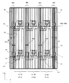
〈画素の構成〉
図1は、本発明の液晶表示装置の一実施例を示す構成図で、液晶を介して対向配置される一対の基板の前記液晶側の面における構成を示す平面図である。
<Pixel configuration>
FIG. 1 is a configuration diagram showing an embodiment of the liquid crystal display device of the present invention, and is a plan view showing a configuration on a surface on the liquid crystal side of a pair of substrates arranged to face each other via a liquid crystal.
すなわち、図1は、図2に示した等価回路に示す部材が形成されたTFT基板TBSと、このTFT基板TBSと液晶を挟んで対向配置された対向基板FBSを示し、該対向基板側から液晶表示装置を透視した平面図となっている。なお、図1のIII−III線における断面図を図3に示す。 That is, FIG. 1 shows a TFT substrate TBS on which members shown in the equivalent circuit shown in FIG. 2 are formed, and a counter substrate FBS arranged opposite to the TFT substrate TBS with a liquid crystal in between. It is the top view which saw through the display apparatus. A sectional view taken along line III-III in FIG. 1 is shown in FIG.
TFT基板TSBは次に示すように構成されている。まず、たとえばガラスからなる基板SUB1(図3参照)があり、この基板SUB1の液晶LC側の面に、下地膜GDL1、GDL2(図3参照)が形成されている。この下地膜GDL1、GDL2は、後述の薄膜トランジスタTFTの半導体層に基板SUB1内の不純物が侵入するのを阻止するようになっている。 The TFT substrate TSB is configured as follows. First, there is a substrate SUB1 (see FIG. 3) made of glass, for example, and base films GDL1 and GDL2 (see FIG. 3) are formed on the surface of the substrate SUB1 on the liquid crystal LC side. The base films GDL1 and GDL2 prevent impurities in the substrate SUB1 from entering a semiconductor layer of a thin film transistor TFT described later.
下地膜GDLの上面には、画素領域ごとに形成される薄膜トランジスタTFTの形成領域にたとえばポリシリコン(p−Si)からなる半導体層PSが形成され、この半導体層PSをも被って絶縁膜GI(図3参照)が形成されている。この絶縁膜GIは薄膜トランジスタTFTの形成領域においてゲート絶縁膜として機能する。 On the upper surface of the base film GDL, a semiconductor layer PS made of, for example, polysilicon (p-Si) is formed in a formation region of the thin film transistor TFT formed for each pixel region, and the insulating film GI ( 3) is formed. This insulating film GI functions as a gate insulating film in the formation region of the thin film transistor TFT.
絶縁膜GIの上面には、ゲート信号線GLが、図中x方向に延在しy方向に並設されて形成されている。この場合、ゲート信号線GLは半導体層PSの中央部を交差するように形成され、その交差部において薄膜トランジスタTFTのゲート電極となるようになっている。 On the upper surface of the insulating film GI, a gate signal line GL is formed so as to extend in the x direction in the drawing and juxtaposed in the y direction. In this case, the gate signal line GL is formed so as to intersect the central portion of the semiconductor layer PS, and becomes the gate electrode of the thin film transistor TFT at the intersecting portion.
また、絶縁膜GIの上面には、ゲート信号線GLをも被って、層間絶縁膜IN1が形成され、この層間絶縁膜IN1の上面には、ドレイン信号線DLが、図中y方向に延在しx方向に並設されて形成されている。ドレイン信号線DLは層間絶縁膜IN1に形成されたスルーホールを通して半導体層PSの一端に電気的に接続されている。ドレイン信号線DLの半導体層PSの接続部は薄膜トランジスタTFTのドレイン電極DTとして機能する。 Further, an interlayer insulating film IN1 is formed on the upper surface of the insulating film GI so as to cover the gate signal line GL, and a drain signal line DL extends in the y direction in the drawing on the upper surface of the interlayer insulating film IN1. And formed side by side in the x direction. The drain signal line DL is electrically connected to one end of the semiconductor layer PS through a through hole formed in the interlayer insulating film IN1. A connection portion of the semiconductor layer PS of the drain signal line DL functions as a drain electrode DT of the thin film transistor TFT.
層間絶縁膜IN1の上面には薄膜トランジスタTFTのソース電極STが形成され、このソース電極STは層間絶縁膜IN1に形成されたスルーホールを通して半導体層PSの他端に電気的に接続されている。ソース電極STは後述の画素電極PXと電気的に接続されるようになっている。 A source electrode ST of the thin film transistor TFT is formed on the upper surface of the interlayer insulating film IN1, and this source electrode ST is electrically connected to the other end of the semiconductor layer PS through a through hole formed in the interlayer insulating film IN1. The source electrode ST is electrically connected to a pixel electrode PX described later.
層間絶縁膜IN1の上面には薄膜トランジスタTFTをも被って保護膜PAS1、保護膜PAS2の順次積層体(図3参照)が形成されている。薄膜トランジスタTFTの液晶LCとの直接の接触を回避させるためである。保護膜PAS1は無機絶縁膜、保護膜PAS2は有機絶縁膜で形成されている。保護膜PAS2を有機絶縁膜としたのは、塗布により形成でき、表面を平坦化できるからである。 A laminated body (see FIG. 3) of a protective film PAS1 and a protective film PAS2 is formed on the upper surface of the interlayer insulating film IN1 so as to cover the thin film transistor TFT. This is to avoid direct contact of the thin film transistor TFT with the liquid crystal LC. The protective film PAS1 is formed of an inorganic insulating film, and the protective film PAS2 is formed of an organic insulating film. The reason why the protective film PAS2 is an organic insulating film is that it can be formed by coating and the surface can be flattened.
保護膜PAS2の上面には、たとえばITO(Indium Tin Oxide)の透明導電層からなる対向電極CT(図3参照)が形成されている。この対向電極CTはたとえば隣接する画素の領域にまで及んで形成される面状の電極からなり、図2に示した電圧対向信号線CLを兼ね備えた構成となっている。なお、この対向電極CTは薄膜トランジスタTFTのソース電極STと重畳する部分において孔(図1において符号HLで示す)が形成されている。スルーホールを通して後述の画素電極PXを前記ソース電極STとの接続をする場合において、対向電極CTと画素電極PXとの電気的短絡を回避するためである。 On the upper surface of the protective film PAS2, a counter electrode CT (see FIG. 3) made of, for example, a transparent conductive layer of ITO (Indium Tin Oxide) is formed. The counter electrode CT is composed of, for example, a planar electrode that extends to an adjacent pixel region, and has a configuration that also includes the voltage counter signal line CL shown in FIG. The counter electrode CT has a hole (indicated by reference numeral HL in FIG. 1) in a portion overlapping the source electrode ST of the thin film transistor TFT. This is to avoid an electrical short circuit between the counter electrode CT and the pixel electrode PX when connecting a pixel electrode PX, which will be described later, to the source electrode ST through a through hole.
対向電極CTの上面には層間絶縁膜IN2が形成され、この層間絶縁膜IN2の上面には各画素領域に画素電極PXが形成されている。この画素電極PXは、たとえばITO(Indium Tin Oxide)の透明導電層から構成されている。また、画素電極PXは、たとえば図中y方向に延在しx方向に並設される複数(たとえば2個)の線状電極からなり、これら線状の電極は、薄膜トランジスタTFT側の端部において互いに接続されている。 An interlayer insulating film IN2 is formed on the upper surface of the counter electrode CT, and a pixel electrode PX is formed in each pixel region on the upper surface of the interlayer insulating film IN2. The pixel electrode PX is made of, for example, a transparent conductive layer of ITO (Indium Tin Oxide). The pixel electrode PX is composed of, for example, a plurality of (for example, two) linear electrodes extending in the y direction and arranged in parallel in the x direction, and these linear electrodes are formed at the end on the thin film transistor TFT side. Are connected to each other.
そして、画素電極PXは、その線状の電極の接続部において、層間絶縁膜IN2、保護膜PAS2、保護膜PAS1に形成されたスルーホールTHを通して薄膜トランジスタTFTのソース電極Sと電気的に接続されるようになっている。 The pixel electrode PX is electrically connected to the source electrode S of the thin film transistor TFT through the through hole TH formed in the interlayer insulating film IN2, the protective film PAS2, and the protective film PAS1 at the connection portion of the linear electrodes. It is like that.
画素電極PXが形成された層間絶縁膜IN2の上面には、画素電極PXをも被って配向膜ORI1が形成されている。この配向膜ORI1は液晶の分子の初期配向方向を決定させるようになっている。 On the upper surface of the interlayer insulating film IN2 on which the pixel electrode PX is formed, an alignment film ORI1 is formed so as to cover the pixel electrode PX. The alignment film ORI1 determines the initial alignment direction of liquid crystal molecules.
上述したTFT基板TSBと液晶LCを介して対向配置される対向基板FSBは次に示すように構成されている。まず、たとえばガラスからなる基板SUB2(図3参照)があり、この基板SUB2の液晶LC側の面にブラックマトリックスBMが形成されている。このブラックマトリックスBMは、たとえばこの実施例では、TFT基板TSB側に形成された該ドレイン信号線DLを被うようにして形成されている。そして、このように図中x方向に並設される各ブラックマトリックスBMは、隣接する3個において、それぞれ、その幅が異なって形成され、また、図中x方向へ3個おきに同じ幅のブラックマトリックスBMが並設されるようになっている。これらブラックマトリックスBMの幅については後に詳述する。 The counter substrate FSB arranged to face the above-described TFT substrate TSB via the liquid crystal LC is configured as follows. First, there is a substrate SUB2 (see FIG. 3) made of glass, for example, and a black matrix BM is formed on the surface of the substrate SUB2 on the liquid crystal LC side. For example, in this embodiment, the black matrix BM is formed so as to cover the drain signal line DL formed on the TFT substrate TSB side. The black matrixes BM arranged side by side in the x direction in the figure are formed with different widths in the three adjacent ones, and have the same width every third piece in the x direction in the figure. Black matrixes BM are arranged side by side. The width of the black matrix BM will be described in detail later.
そして、隣接するブラックマトリックスBMの間にそれぞれカラーフィルタFLが形成され、これらカラーフィルタFLは図中x方向に、たとえば、緑色のカラーフィルタFL(G)、赤色のカラーフィルタFL(R)、青色のカラーフィルタFL(B)、緑色のカラーフィルタFL(G)、赤色のカラーフィルタFL(R)、……という順番で配置されている。赤色のカラーフィルタFL(R)で被われる画素は赤色を担当する画素(以下、赤色画素PX(R)という)、青色のカラーフィルタFL(B)で被われる画素は青色を担当する画素(以下、青色画素PX(B)という)、緑色のカラーフィルタFL(G)で被われる画素は緑色を担当する画素(以下、緑色画素PX(G)という)となり、図中x方向に隣接する色の異なる3つの画素でカラー表示用の単位画素を構成するようになっている。 Color filters FL are formed between adjacent black matrices BM, and these color filters FL are arranged in the x direction in the drawing, for example, a green color filter FL (G), a red color filter FL (R), and a blue color. Are arranged in the order of color filter FL (B), green color filter FL (G), red color filter FL (R),. Pixels covered with the red color filter FL (R) are pixels responsible for red (hereinafter referred to as red pixels PX (R)), and pixels covered with the blue color filter FL (B) are pixels responsible for blue (hereinafter referred to as red pixels PX (R)). , A pixel covered with the green color filter FL (G) is a pixel in charge of green (hereinafter referred to as a green pixel PX (G)) and has a color adjacent to the x direction in the figure. A unit pixel for color display is constituted by three different pixels.
これらカラーフィルタFLの上面にはたとえば樹脂膜からなるオーバーコート膜OCが形成され、その表面は平坦化されている。そして、オーバーコート膜OCの上面には配向膜ORI2が形成され、この配向膜ORI1は液晶LCの分子の初期配向方向を決定させるようになっている。 An overcoat film OC made of, for example, a resin film is formed on the upper surfaces of these color filters FL, and the surface thereof is flattened. An alignment film ORI2 is formed on the upper surface of the overcoat film OC, and this alignment film ORI1 determines the initial alignment direction of the molecules of the liquid crystal LC.
なお、図示していないが、基板SUB1の基板SUB2と反対側の面にはバックライトが配置されている。このバックライトは青色を帯びた光源を備えたものとなっている。画素の透過コントラスト比が大きくなるように液晶LCのリターデーションを設定した場合、液晶を透過する光は黄色味を帯びることから、黄色の補色である青色味を帯びた光源を用いるのが好ましいからである。 Although not shown, a backlight is disposed on the surface of the substrate SUB1 opposite to the substrate SUB2. This backlight has a blue light source. When the retardation of the liquid crystal LC is set so as to increase the transmission contrast ratio of the pixel, the light transmitted through the liquid crystal is yellowish, so it is preferable to use a light source with a blue taste that is a complementary color of yellow. It is.
ここで、上述したブラックマトリックスBMの幅について説明する。赤色画素PX(R)と青色画素PX(B)の間に配置されるブラックマトリックスBMの幅をWrb、緑色画素PX(G)と赤色画素PX(R)の間に配置されるブラックマトリックスBMの幅をWgr、青色画素PX(B)と緑色画素PX(G)の間に配置されるブラックマトリックスBMの幅をWbgとした場合、Wrb≠Wgr≠Wbgであり、Wrb>Wbg>Wgrが成立するようになっている。 Here, the width of the black matrix BM will be described. The width of the black matrix BM disposed between the red pixel PX (R) and the blue pixel PX (B) is Wrb, and the width of the black matrix BM disposed between the green pixel PX (G) and the red pixel PX (R). When the width is Wgr and the width of the black matrix BM arranged between the blue pixel PX (B) and the green pixel PX (G) is Wbg, Wrb ≠ Wgr ≠ Wbg and Wrb> Wbg> Wgr is satisfied. It is like that.
このように液晶表示装置を構成した場合、赤色画素PX(R)の単色表示において、隣接する青色画素PX(B)側の斜め方向から観察した場合、青色が混ざって生じる混色の不都合が光源の青色味によって強調され顕著となる。このため、青色が混ざる光を赤色画素PX(R)と青色画素PX(B)の間のブラックマトリックスBMによって遮光する必要があり、その幅Wrbは太くせざるを得なくなる。 When the liquid crystal display device is configured in this way, in the monochromatic display of the red pixel PX (R), when observed from an oblique direction on the side of the adjacent blue pixel PX (B), the inconvenience of the color mixture caused by the mixture of blue is a problem of the light source. It is emphasized by the blue color and becomes noticeable. For this reason, it is necessary to block light mixed with blue by the black matrix BM between the red pixel PX (R) and the blue pixel PX (B), and the width Wrb must be increased.
一方、赤の単色表示において、隣接する緑色画素側の斜め方向から観察した場合、緑色が混ざって生じる混色の不都合は、青色が混ざって生じる混色の不都合と比較して視認しづらくなる。 On the other hand, in red single color display, when observed from an oblique direction on the side of an adjacent green pixel, the inconvenience of color mixing caused by mixing green becomes difficult to visually recognize compared to the inconvenience of color mixing caused by mixing blue.
そして、緑色の単色表示において隣接する青色画素PX(B)側の斜め方向からの観察のおける、混色の視認程度は、赤色画素PX(R)の単色表示における青色の混色度合より小さく、赤色画素PX(R)の単色表示における緑色の混色度合より大きくなることが確認される。したがって、青色画素と緑色画素の間に配置されるブラックマトリックスBMの幅をWbgとした場合、Wrb>Wbg>Wgrの関係が成立するように、Wbgを設定することができる。 In the green single color display, the degree of visual recognition of the mixed color that can be observed from the oblique direction on the side of the adjacent blue pixel PX (B) is smaller than the degree of blue mixed color in the single color display of the red pixel PX (R). It is confirmed that it is larger than the green color mixture degree in the single color display of PX (R). Therefore, when the width of the black matrix BM arranged between the blue pixel and the green pixel is Wbg, Wbg can be set so that the relationship of Wrb> Wbg> Wgr is established.
以上説明したように、本実施例による液晶表示装置によれば、ブラックマトリックスGMの幅を一律に太くする場合と比較し、各画素の開口率を向上させることができる。 As described above, according to the liquid crystal display device according to this embodiment, the aperture ratio of each pixel can be improved as compared with the case where the width of the black matrix GM is uniformly increased.
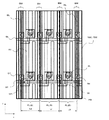
(実施例2)
図4は、本発明による液晶表示装置の他の実施例を示す構成図で、図1に対応した図となっている。
(Example 2)
FIG. 4 is a block diagram showing another embodiment of the liquid crystal display device according to the present invention and corresponds to FIG.
図4において、図1の場合の構成と比較した場合、まず、緑色画素PX(G)と赤色画素PX(R)の間のブラックマトリックスBMの幅、赤色画素PX(R)と青色画素PX(B)の間のブラックマトリックスBMの幅、青色画素PX(B)と緑色画素PX(G)の間のブラックマトリックスBMの幅は、それぞれ、等しく構成されている。各ブラックマトリックスBMの幅は、画素の開口率の観点から許容できる範囲で設定することができる。 In FIG. 4, when compared with the configuration of FIG. 1, first, the width of the black matrix BM between the green pixel PX (G) and the red pixel PX (R), the red pixel PX (R) and the blue pixel PX ( The width of the black matrix BM during B) and the width of the black matrix BM between the blue pixel PX (B) and the green pixel PX (G) are configured to be equal. The width of each black matrix BM can be set in an allowable range from the viewpoint of the aperture ratio of the pixels.
そして、赤色画素PX(R)と青色画素PX(B)の間のブラックマトリックスBMは、このブラックマトリックスBMによって被われるドレイン信号線DLに対して青色画素PX(B)側へ若干ずれて形成されている。これにより、赤色画素PX(R)の単色表示において、隣接する青色画素PX(B)側の斜め方向から観察した場合に、青色の光が混ざってしまうのを、青色画素PX(B)側へずらして配置させたブラックマトリックスBMによって遮光させるようにしている。なお、この実施例において各ドレイン信号線はその並設方向において等間隔に配置されたものとなっている。 The black matrix BM between the red pixel PX (R) and the blue pixel PX (B) is formed with a slight shift toward the blue pixel PX (B) with respect to the drain signal line DL covered by the black matrix BM. ing. Thereby, in the monochromatic display of the red pixel PX (R), when observed from an oblique direction on the side of the adjacent blue pixel PX (B), the blue light is mixed into the blue pixel PX (B) side. The black matrix BM arranged in a shifted manner is shielded from light. In this embodiment, the drain signal lines are arranged at equal intervals in the parallel arrangement direction.
また、緑色画素PX(G)と青色画素PX(B)の間のブラックマトリックスBM、及び緑色画素PX(G)と赤色画素PX(R)の間のブラックマトリックスBMは、このブラックマトリックスBMによって被われるドレイン信号線DLに対してずれがなく、それらの中心線をほぼ一致させて形成されている。緑色画素PX(G)の単色表示において、隣接する青色画素PX(B)側の斜め方向から観察した場合に青色が混ざっても、混色は視認し難く、緑色画素PX(G)と青色画素PX(B)の間のブラックマトリックスBMは通常の形態で形成されるようになっている。 Further, the black matrix BM between the green pixel PX (G) and the blue pixel PX (B) and the black matrix BM between the green pixel PX (G) and the red pixel PX (R) are covered by the black matrix BM. There is no deviation with respect to the drain signal line DL, and their center lines are substantially coincident. In the monochromatic display of the green pixel PX (G), even when blue is mixed when observed from an oblique direction on the adjacent blue pixel PX (B) side, the mixed color is difficult to visually recognize, and the green pixel PX (G) and the blue pixel PX The black matrix BM between (B) is formed in a normal form.
このようなことから、この実施例では、赤色画素PX(R)とこれに隣接する青色画素PX(B)の間に配置されるブラックマトリックスBMの中心と赤色画素PX(R)とこれに隣接する緑色画素PX(G)の間に配置されるブラックマトリックスBMの中心との距離をLrとし、青色画素PX(B)とこれに隣接する緑色画素PX(G)の間に配置されるブラックマトリックスBMの中心と青色画素PX(B)とこれに隣接する赤色画素PX(R)の間に配置されるブラックマトリックスの中心との距離をLbとし、緑色画素PX(G)とこれに隣接する青色画素PX(B)の間に配置されるブラックマトリックスの中心と緑色画素PX(G)とこれに隣接する赤色画素PX(R)の間に配置されるブラックマトリックスBMの中心との距離をLgとした場合に、Lr>Lg>Lbが成立する関係となる。 For this reason, in this embodiment, the center of the black matrix BM and the red pixel PX (R) adjacent to the red pixel PX (R) and the blue pixel PX (B) adjacent thereto are adjacent to this. The black matrix disposed between the blue pixel PX (B) and the adjacent green pixel PX (G) is Lr, and the distance from the center of the black matrix BM disposed between the green pixels PX (G) to be performed is Lr. The distance between the center of the BM and the center of the black matrix disposed between the blue pixel PX (B) and the adjacent red pixel PX (R) is Lb, and the green pixel PX (G) and the adjacent blue color The center of the black matrix disposed between the pixels PX (B) and the center of the black matrix BM disposed between the green pixel PX (G) and the red pixel PX (R) adjacent thereto. A release in the case of the Lg, the relationship Lr> Lg> Lb is satisfied.
このように構成された液晶表示装置は、表示面を斜め方向から見た場合の色の混色を回避させるのに、各ブラックマトリックスを最小限の幅に設定することができ、したがって、画素の開口率を向上させることができる。 The liquid crystal display device configured as described above can set each black matrix to a minimum width to avoid color mixture when the display surface is viewed from an oblique direction. The rate can be improved.
本実施例においては、IPS型の液晶表示装置の例について取り上げたが、本提案の技術の適用はIPS型の液晶表示装置のみに止まらないことは言うまでもない。つまり、いわゆる垂直配向(VA;Vertical Alignment)型の液晶表示装置、TN(Twisted Nematic)型の液晶表示装置に本技術を適用することで、混色を回避と開口率向上の両立が可能である。 In this embodiment, an example of an IPS type liquid crystal display device has been taken up. However, it goes without saying that the application of the proposed technique is not limited to an IPS type liquid crystal display device. That is, by applying the present technology to a so-called vertical alignment (VA) type liquid crystal display device and TN (Twisted Nematic) type liquid crystal display device, it is possible to avoid color mixing and improve the aperture ratio.
TBS……TFT基板、FBS……対向基板、SUB1、SUB2……基板、GL……ゲート信号線、DL……ドレイン信号線、CL……対向電圧信号線、TFT……薄膜トランジスタ、DT……ドレイン電極、ST……ソース電極、PX……画素電極、CT……対向電極、GDL1、GDL2……下地層、GI……絶縁膜(ゲート絶縁膜)、IN1、IN2……層間絶縁膜、PAS1、PAS2……保護膜、ORI1、ORI2……配向膜、BM……ブラックマトリックス、FL……カラーフィルタ、FL(R)……赤色のカラーフィルタ、FL(G)……緑色のカラーフィルタ、FL(B)……青色のカラーフィルタ、PX(R)……赤色画素、PX(G)……緑色画素、PX(B)……青色画素、OC……オーバーコート膜。 TBS ... TFT substrate, FBS ... Counter substrate, SUB1, SUB2 ... Substrate, GL ... Gate signal line, DL ... Drain signal line, CL ... Counter voltage signal line, TFT ... Thin film transistor, DT ... Drain Electrode, ST ... Source electrode, PX ... Pixel electrode, CT ... Counter electrode, GDL1, GDL2 ... Underlayer, GI ... Insulating film (gate insulating film), IN1, IN2 ... Interlayer insulating film, PAS1, PAS2 ... Protective film, ORI1, ORI2 ... Alignment film, BM ... Black matrix, FL ... Color filter, FL (R) ... Red color filter, FL (G) ... Green color filter, FL ( B): Blue color filter, PX (R): Red pixel, PX (G): Green pixel, PX (B): Blue pixel, OC: Overcoat film.
Claims (4)
前記一対の基板のうち一方の基板に形成された遮光膜およびカラーフィルタと、
前記カラーフィルタの色によって定まる赤色サブピクセル、緑色サブピクセル、および青色サブピクセルとを有し、
前記赤色サブピクセル、前記緑色サブピクセル、および青色サブピクセルは、第1の方向に同色が隣接しないように配置され、
前記遮光膜は、互いに隣接する前記赤色サブピクセル、前記緑色サブピクセル、および前記青色サブピクセルの境界部に配置され、
前記遮光膜の幅を、
前記赤色サブピクセルと前記青色サブピクセルの境界部に配置される前記遮光膜の幅をWrb、前記緑色サブピクセルと前記赤色サブピクセルの境界部に配置される前記遮光膜の幅をWgr、前記青色サブピクセルと前記緑色サブピクセルの境界部に配置される前記遮光膜の幅をWbgとするとき、
Wrb>Wbg>Wgr
が成立するように形成した
ことを特徴とする液晶表示装置。 A pair of substrates disposed opposite each other with a liquid crystal sandwiched between them;
A light-shielding film and a color filter formed on one of the pair of substrates;
A red subpixel, a green subpixel, and a blue subpixel determined by the color of the color filter;
The red sub-pixel, the green sub-pixel, and the blue sub-pixel are arranged such that the same color is not adjacent in the first direction;
The light shielding film is disposed at a boundary portion between the red subpixel, the green subpixel, and the blue subpixel adjacent to each other,
The width of the light shielding film,
Wrb the width of the light shielding film disposed on the boundary of the blue subpixel and the red subpixel, the green subpixel and the red Sabupikuse Le of Wgr the width of the light shielding film disposed on the boundary portion, the blue when the width of the light shielding film and the subpixel Ru is disposed in a boundary portion of the green sub-pixel and WBG,
Wrb>Wbg> Wgr
A liquid crystal display device formed to satisfy the above .
前記遮光膜は、平面的に観た場合、前記ドレイン信号線を被って形成されている
ことを特徴とする請求項1に記載の液晶表示装置。 A drain signal line for supplying a video signal to each pixel is formed on the liquid crystal side surface of the other substrate of the pair of substrates,
The liquid crystal display device according to claim 1, wherein the light shielding film is formed so as to cover the drain signal line when viewed in plan .
前記青色サブピクセルとこれに隣接する前記緑色サブピクセルの境界部に配置される前記遮光膜の幅の中心線と、前記青色サブピクセルとこれに隣接する前記赤色サブピクセルの境界部に配置される前記遮光膜の幅の中心線との距離をLbとするとき、
Lr>Lb
が成立するように形成した
ことを特徴とする請求項1又は2に記載の液晶表示装置。 A center line of the width of the light shielding film disposed at a boundary between the red subpixel and the blue subpixel adjacent thereto, and a boundary between the red subpixel and the green subpixel adjacent thereto. The distance from the center line of the width of the light shielding film is Lr,
A center line of the width of the light shielding film disposed at a boundary between the blue subpixel and the green subpixel adjacent thereto, and a boundary between the blue subpixel and the red subpixel adjacent thereto. When the distance from the center line of the width of the light shielding film is Lb,
Lr> Lb
There the liquid crystal display device according to claim 1 or 2, characterized in that it has formed to stand.
Lr>Lg>Lb
が成立するように形成した
ことを特徴とする請求項3に記載の液晶表示装置。 A center line of the width of the light shielding film disposed at a boundary between the green subpixel and the blue subpixel adjacent thereto, and a boundary between the green subpixel and the red subpixel adjacent thereto. When the distance from the center line of the width of the light shielding film is Lg,
Lr>Lg> Lb
The liquid crystal display device according to claim 3, wherein the liquid crystal display device is formed so that
Priority Applications (6)
| Application Number | Priority Date | Filing Date | Title |
|---|---|---|---|
| JP2008171954A JP5301895B2 (en) | 2008-07-01 | 2008-07-01 | Liquid crystal display |
| US12/495,910 US8269925B2 (en) | 2008-07-01 | 2009-07-01 | Liquid crystal display device with light blocking film overlapping drain signal line |
| US13/605,195 US8395730B2 (en) | 2008-07-01 | 2012-09-06 | Liquid crystal display device |
| US13/792,498 US8749739B2 (en) | 2008-07-01 | 2013-03-11 | Liquid crystal display device |
| US14/289,000 US9482894B2 (en) | 2008-07-01 | 2014-05-28 | Liquid crystal display device |
| US15/278,100 US9983429B2 (en) | 2008-07-01 | 2016-09-28 | Liquid crystal display device |
Applications Claiming Priority (1)
| Application Number | Priority Date | Filing Date | Title |
|---|---|---|---|
| JP2008171954A JP5301895B2 (en) | 2008-07-01 | 2008-07-01 | Liquid crystal display |
Publications (3)
| Publication Number | Publication Date |
|---|---|
| JP2010014760A JP2010014760A (en) | 2010-01-21 |
| JP2010014760A5 JP2010014760A5 (en) | 2011-05-26 |
| JP5301895B2 true JP5301895B2 (en) | 2013-09-25 |
Family
ID=41463968
Family Applications (1)
| Application Number | Title | Priority Date | Filing Date |
|---|---|---|---|
| JP2008171954A Active JP5301895B2 (en) | 2008-07-01 | 2008-07-01 | Liquid crystal display |
Country Status (2)
| Country | Link |
|---|---|
| US (5) | US8269925B2 (en) |
| JP (1) | JP5301895B2 (en) |
Cited By (1)
| Publication number | Priority date | Publication date | Assignee | Title |
|---|---|---|---|---|
| US9618806B2 (en) | 2014-11-26 | 2017-04-11 | Samsung Display Co., Ltd. | Display device having a multi-portion light blocking member |
Families Citing this family (36)
| Publication number | Priority date | Publication date | Assignee | Title |
|---|---|---|---|---|
| JP5301895B2 (en) * | 2008-07-01 | 2013-09-25 | 株式会社ジャパンディスプレイ | Liquid crystal display |
| JP4756178B2 (en) * | 2009-04-01 | 2011-08-24 | 奇美電子股▲ふん▼有限公司 | Display device |
| US8293640B2 (en) | 2010-05-06 | 2012-10-23 | Victory Gain Group Corporation | Semiconductor structure and manufacturing method thereof |
| CN102985855B (en) | 2010-06-16 | 2015-04-29 | 松下电器产业株式会社 | El display panel, EL display device provided with EL display panel, organic EL display device, and method for manufacturing EL display panel |
| WO2011158287A1 (en) * | 2010-06-16 | 2011-12-22 | パナソニック株式会社 | El display panel, el display device provided with el display panel, organic el display device, and method for manufacturing el display panel |
| JP2013196854A (en) * | 2012-03-16 | 2013-09-30 | Sharp Corp | Fluorescent substrate and display device including the same |
| KR101994972B1 (en) * | 2012-06-20 | 2019-07-02 | 삼성디스플레이 주식회사 | Liquid crystal display |
| US9291859B2 (en) * | 2012-06-20 | 2016-03-22 | Samsung Display Co., Ltd. | Liquid crystal display |
| SG11201407832XA (en) * | 2012-06-22 | 2015-01-29 | Toray Industries | Colour filter and display device |
| WO2014038436A1 (en) * | 2012-09-04 | 2014-03-13 | シャープ株式会社 | Liquid crystal display device |
| KR101997745B1 (en) * | 2013-01-25 | 2019-07-09 | 삼성디스플레이 주식회사 | Liquid crystal display |
| CN103455202B (en) * | 2013-08-28 | 2015-11-25 | 合肥京东方光电科技有限公司 | In-cell touch panel, its preparation method and display device |
| JP2015069119A (en) * | 2013-09-30 | 2015-04-13 | パナソニック液晶ディスプレイ株式会社 | Display device |
| TWI548913B (en) * | 2014-04-01 | 2016-09-11 | 群創光電股份有限公司 | Fringe field switching liquid crystal display panel and display device |
| KR102179011B1 (en) * | 2014-04-03 | 2020-11-18 | 삼성디스플레이 주식회사 | Display device |
| TWI534516B (en) * | 2014-07-30 | 2016-05-21 | 群創光電股份有限公司 | Display panel and display device |
| KR102205863B1 (en) * | 2014-08-01 | 2021-01-22 | 삼성디스플레이 주식회사 | Display device |
| CN104460146A (en) * | 2014-11-13 | 2015-03-25 | 深圳市华星光电技术有限公司 | BOA type liquid crystal display panel and manufacturing method thereof |
| JP2016148807A (en) * | 2015-02-13 | 2016-08-18 | 株式会社ジャパンディスプレイ | Liquid crystal display device |
| TWI548915B (en) * | 2015-04-10 | 2016-09-11 | 群創光電股份有限公司 | Display panel |
| CN106154619B (en) * | 2015-04-10 | 2023-06-02 | 群创光电股份有限公司 | Display panel |
| CN104865737B (en) * | 2015-06-15 | 2017-07-25 | 京东方科技集团股份有限公司 | A kind of display panel, its driving method and display device |
| US10139664B2 (en) * | 2015-06-23 | 2018-11-27 | Panasonic Liquid Crystal Display Co., Ltd. | Preventing color mixing in liquid crystal display devices |
| CN105093653B (en) * | 2015-08-26 | 2018-05-29 | 深圳市华星光电技术有限公司 | A kind of color membrane substrates and curved-surface display device |
| CN105278152B (en) * | 2015-11-12 | 2018-07-27 | 深圳市华星光电技术有限公司 | Improve the liquid crystal display of big visual angle colour cast |
| JP2017181820A (en) | 2016-03-30 | 2017-10-05 | パナソニック液晶ディスプレイ株式会社 | On-vehicle device with curved display |
| US9709866B1 (en) | 2016-03-30 | 2017-07-18 | Panasonic Liquid Crystal Display Co., Ltd. | Liquid crystal display device |
| KR102655677B1 (en) * | 2016-07-04 | 2024-04-11 | 티씨엘 차이나 스타 옵토일렉트로닉스 테크놀로지 컴퍼니 리미티드 | Display device |
| CN108333843B (en) | 2017-01-20 | 2020-11-13 | 京东方科技集团股份有限公司 | Double-grid line array substrate and display device |
| CN107272289B (en) * | 2017-07-06 | 2020-05-22 | 厦门天马微电子有限公司 | Liquid crystal display panel and liquid crystal display device |
| US10345638B2 (en) * | 2017-08-01 | 2019-07-09 | Shenzhen China Star Optoelectronics Technology Co., Ltd | Display panel and display device |
| CN109643462B (en) | 2018-11-21 | 2023-07-04 | 京东方科技集团股份有限公司 | Real-time image processing method based on rendering engine and display device |
| CN109298577B (en) * | 2018-11-30 | 2022-04-12 | 上海中航光电子有限公司 | Display panel and display device |
| CN109445175A (en) * | 2019-01-10 | 2019-03-08 | 惠科股份有限公司 | Display device, colored filter and colorful optical filter preparation method |
| CN109884819A (en) * | 2019-04-15 | 2019-06-14 | 深圳市华星光电技术有限公司 | Liquid crystal display panel and liquid crystal display device |
| CN113053973B (en) * | 2021-03-11 | 2023-04-07 | 云南创视界光电科技有限公司 | Display substrate, color film substrate, display panel and display device |
Family Cites Families (21)
| Publication number | Priority date | Publication date | Assignee | Title |
|---|---|---|---|---|
| JPH0623035U (en) * | 1992-02-17 | 1994-03-25 | 日本電気ホームエレクトロニクス株式会社 | Liquid crystal display |
| JP2952171B2 (en) * | 1994-12-21 | 1999-09-20 | キヤノン株式会社 | Color filter, manufacturing method thereof, and liquid crystal panel |
| JP3207136B2 (en) | 1997-07-17 | 2001-09-10 | 三菱電機株式会社 | Liquid crystal display |
| JP2000066237A (en) * | 1998-08-25 | 2000-03-03 | Sony Corp | Liquid crystal display device |
| KR100887325B1 (en) * | 1999-09-07 | 2009-03-06 | 가부시키가이샤 히타치세이사쿠쇼 | Liquid crystal display |
| JP3792485B2 (en) * | 2000-06-02 | 2006-07-05 | Nec液晶テクノロジー株式会社 | Active matrix liquid crystal display device |
| JP2002323616A (en) * | 2001-04-26 | 2002-11-08 | Canon Inc | Color filter, its manufacturing method and liquid crystal element using the color filter |
| CN1210606C (en) * | 2001-08-29 | 2005-07-13 | 精工爱普生株式会社 | Electrooptical device and electronic apparatus |
| JP2003107447A (en) * | 2001-09-27 | 2003-04-09 | Sharp Corp | Plasma address liquid crystal display device |
| KR100447125B1 (en) * | 2002-03-08 | 2004-09-04 | 엘지전자 주식회사 | Plasma Display Panel |
| CN1324363C (en) * | 2002-05-04 | 2007-07-04 | 三星电子株式会社 | LCD device and filtering color picec array board |
| JP2005062692A (en) * | 2003-08-19 | 2005-03-10 | Internatl Business Mach Corp <Ibm> | Color display device, optical element, and method for manufacturing color display device |
| JP4156476B2 (en) | 2003-09-04 | 2008-09-24 | 株式会社 日立ディスプレイズ | Liquid crystal display |
| JP4111180B2 (en) * | 2004-09-02 | 2008-07-02 | セイコーエプソン株式会社 | Liquid crystal display device and electronic device |
| JP2006220711A (en) * | 2005-02-08 | 2006-08-24 | Seiko Epson Corp | Liquid crystal device, substrate for liquid crystal device, and electronic appliance |
| CN101410882B (en) * | 2006-03-30 | 2011-06-22 | 夏普株式会社 | Display device and color filter substrate |
| JP4232807B2 (en) * | 2006-09-06 | 2009-03-04 | セイコーエプソン株式会社 | Electro-optical device and electronic apparatus |
| TWI341399B (en) * | 2006-12-15 | 2011-05-01 | Chimei Innolux Corp | Liquid crystal panel and liquid crystal display device |
| KR100796126B1 (en) * | 2007-02-07 | 2008-01-21 | 삼성에스디아이 주식회사 | Liquid crystal display device and fabrication method thereof |
| JP5534655B2 (en) * | 2008-05-26 | 2014-07-02 | セイコーエプソン株式会社 | ELECTRO-OPTICAL DEVICE, MANUFACTURING METHOD THEREOF, AND ELECTRONIC DEVICE |
| JP5301895B2 (en) * | 2008-07-01 | 2013-09-25 | 株式会社ジャパンディスプレイ | Liquid crystal display |
-
2008
- 2008-07-01 JP JP2008171954A patent/JP5301895B2/en active Active
-
2009
- 2009-07-01 US US12/495,910 patent/US8269925B2/en active Active
-
2012
- 2012-09-06 US US13/605,195 patent/US8395730B2/en active Active
-
2013
- 2013-03-11 US US13/792,498 patent/US8749739B2/en active Active
-
2014
- 2014-05-28 US US14/289,000 patent/US9482894B2/en active Active
-
2016
- 2016-09-28 US US15/278,100 patent/US9983429B2/en active Active
Cited By (1)
| Publication number | Priority date | Publication date | Assignee | Title |
|---|---|---|---|---|
| US9618806B2 (en) | 2014-11-26 | 2017-04-11 | Samsung Display Co., Ltd. | Display device having a multi-portion light blocking member |
Also Published As
| Publication number | Publication date |
|---|---|
| US20100001939A1 (en) | 2010-01-07 |
| JP2010014760A (en) | 2010-01-21 |
| US20130194531A1 (en) | 2013-08-01 |
| US20120327340A1 (en) | 2012-12-27 |
| US20140267963A1 (en) | 2014-09-18 |
| US20170017111A1 (en) | 2017-01-19 |
| US8749739B2 (en) | 2014-06-10 |
| US8269925B2 (en) | 2012-09-18 |
| US9482894B2 (en) | 2016-11-01 |
| US8395730B2 (en) | 2013-03-12 |
| US9983429B2 (en) | 2018-05-29 |
Similar Documents
| Publication | Publication Date | Title |
|---|---|---|
| JP5301895B2 (en) | Liquid crystal display | |
| JP5500712B2 (en) | LCD panel | |
| US9176339B2 (en) | Liquid crystal display device | |
| US9151994B2 (en) | Display panel | |
| JP5888557B2 (en) | Liquid crystal display | |
| JP6334179B2 (en) | Display device | |
| WO2009122864A1 (en) | Color filter substrate and liquid crystal display device | |
| KR102051563B1 (en) | Liquid crystal display | |
| US9841642B2 (en) | Liquid crystal display device | |
| JP2011048170A (en) | Liquid crystal display device | |
| US7692745B2 (en) | Transflective liquid crystal display device having particular pixel electrodes and counter electrodes arrangement | |
| JP5512158B2 (en) | Display device | |
| US9684200B2 (en) | Liquid crystal display device | |
| JP5681822B2 (en) | LCD panel | |
| JP7398926B2 (en) | liquid crystal display device | |
| JP5914274B2 (en) | Liquid crystal display | |
| JP2010139919A (en) | Liquid crystal display panel for ecb mode | |
| JP6395903B2 (en) | Display device | |
| KR101325436B1 (en) | Liquid crystal display panel, and method for manufacturing the same | |
| WO2012050053A1 (en) | Liquid crystal display device | |
| JP2010072506A (en) | Liquid crystal display |
Legal Events
| Date | Code | Title | Description |
|---|---|---|---|
| A711 | Notification of change in applicant |
Free format text: JAPANESE INTERMEDIATE CODE: A712 Effective date: 20110218 |
|
| RD03 | Notification of appointment of power of attorney |
Free format text: JAPANESE INTERMEDIATE CODE: A7423 Effective date: 20110218 |
|
| A521 | Request for written amendment filed |
Free format text: JAPANESE INTERMEDIATE CODE: A523 Effective date: 20110407 |
|
| A621 | Written request for application examination |
Free format text: JAPANESE INTERMEDIATE CODE: A621 Effective date: 20110407 |
|
| A977 | Report on retrieval |
Free format text: JAPANESE INTERMEDIATE CODE: A971007 Effective date: 20120822 |
|
| A131 | Notification of reasons for refusal |
Free format text: JAPANESE INTERMEDIATE CODE: A131 Effective date: 20120828 |
|
| A521 | Request for written amendment filed |
Free format text: JAPANESE INTERMEDIATE CODE: A523 Effective date: 20121001 |
|
| TRDD | Decision of grant or rejection written | ||
| A01 | Written decision to grant a patent or to grant a registration (utility model) |
Free format text: JAPANESE INTERMEDIATE CODE: A01 Effective date: 20130528 |
|
| A61 | First payment of annual fees (during grant procedure) |
Free format text: JAPANESE INTERMEDIATE CODE: A61 Effective date: 20130620 |
|
| R150 | Certificate of patent or registration of utility model |
Ref document number: 5301895 Country of ref document: JP Free format text: JAPANESE INTERMEDIATE CODE: R150 Free format text: JAPANESE INTERMEDIATE CODE: R150 |
|
| R250 | Receipt of annual fees |
Free format text: JAPANESE INTERMEDIATE CODE: R250 |
|
| R250 | Receipt of annual fees |
Free format text: JAPANESE INTERMEDIATE CODE: R250 |
|
| R250 | Receipt of annual fees |
Free format text: JAPANESE INTERMEDIATE CODE: R250 |
|
| R250 | Receipt of annual fees |
Free format text: JAPANESE INTERMEDIATE CODE: R250 |
|
| R250 | Receipt of annual fees |
Free format text: JAPANESE INTERMEDIATE CODE: R250 |
|
| R250 | Receipt of annual fees |
Free format text: JAPANESE INTERMEDIATE CODE: R250 |
|
| R250 | Receipt of annual fees |
Free format text: JAPANESE INTERMEDIATE CODE: R250 |
|
| R250 | Receipt of annual fees |
Free format text: JAPANESE INTERMEDIATE CODE: R250 |
|
| S111 | Request for change of ownership or part of ownership |
Free format text: JAPANESE INTERMEDIATE CODE: R313117 |
|
| R350 | Written notification of registration of transfer |
Free format text: JAPANESE INTERMEDIATE CODE: R350 |