JP5300714B2 - Process chamber for dielectric gap filling - Google Patents
Process chamber for dielectric gap filling Download PDFInfo
- Publication number
- JP5300714B2 JP5300714B2 JP2009513438A JP2009513438A JP5300714B2 JP 5300714 B2 JP5300714 B2 JP 5300714B2 JP 2009513438 A JP2009513438 A JP 2009513438A JP 2009513438 A JP2009513438 A JP 2009513438A JP 5300714 B2 JP5300714 B2 JP 5300714B2
- Authority
- JP
- Japan
- Prior art keywords
- precursor
- substrate
- deposition chamber
- dielectric
- deposition
- Prior art date
- Legal status (The legal status is an assumption and is not a legal conclusion. Google has not performed a legal analysis and makes no representation as to the accuracy of the status listed.)
- Active
Links
- 238000000034 method Methods 0.000 title description 43
- 230000008569 process Effects 0.000 title description 39
- 238000011049 filling Methods 0.000 title description 5
- 239000002243 precursor Substances 0.000 claims abstract description 249
- 230000008021 deposition Effects 0.000 claims abstract description 192
- 239000000758 substrate Substances 0.000 claims abstract description 157
- 238000009826 distribution Methods 0.000 claims abstract description 30
- 238000011065 in-situ storage Methods 0.000 claims abstract description 5
- 239000007789 gas Substances 0.000 claims description 36
- QVGXLLKOCUKJST-UHFFFAOYSA-N atomic oxygen Chemical compound [O] QVGXLLKOCUKJST-UHFFFAOYSA-N 0.000 claims description 22
- 230000009969 flowable effect Effects 0.000 claims description 20
- XUIMIQQOPSSXEZ-UHFFFAOYSA-N Silicon Chemical group [Si] XUIMIQQOPSSXEZ-UHFFFAOYSA-N 0.000 claims description 18
- 229910052710 silicon Inorganic materials 0.000 claims description 18
- 239000010703 silicon Substances 0.000 claims description 18
- 238000010438 heat treatment Methods 0.000 claims description 15
- -1 DEMS Chemical compound 0.000 claims description 14
- 230000009977 dual effect Effects 0.000 claims description 9
- 230000015572 biosynthetic process Effects 0.000 claims description 8
- LFQCEHFDDXELDD-UHFFFAOYSA-N tetramethyl orthosilicate Chemical compound CO[Si](OC)(OC)OC LFQCEHFDDXELDD-UHFFFAOYSA-N 0.000 claims description 8
- 238000006243 chemical reaction Methods 0.000 claims description 7
- BOTDANWDWHJENH-UHFFFAOYSA-N Tetraethyl orthosilicate Chemical compound CCO[Si](OCC)(OCC)OCC BOTDANWDWHJENH-UHFFFAOYSA-N 0.000 claims description 6
- WZJUBBHODHNQPW-UHFFFAOYSA-N 2,4,6,8-tetramethyl-1,3,5,7,2$l^{3},4$l^{3},6$l^{3},8$l^{3}-tetraoxatetrasilocane Chemical compound C[Si]1O[Si](C)O[Si](C)O[Si](C)O1 WZJUBBHODHNQPW-UHFFFAOYSA-N 0.000 claims description 4
- HMMGMWAXVFQUOA-UHFFFAOYSA-N octamethylcyclotetrasiloxane Chemical compound C[Si]1(C)O[Si](C)(C)O[Si](C)(C)O[Si](C)(C)O1 HMMGMWAXVFQUOA-UHFFFAOYSA-N 0.000 claims description 4
- BLRPTPMANUNPDV-UHFFFAOYSA-N Silane Chemical group [SiH4] BLRPTPMANUNPDV-UHFFFAOYSA-N 0.000 claims description 3
- 229910000077 silane Inorganic materials 0.000 claims description 3
- CXQXSVUQTKDNFP-UHFFFAOYSA-N octamethyltrisiloxane Chemical compound C[Si](C)(C)O[Si](C)(C)O[Si](C)(C)C CXQXSVUQTKDNFP-UHFFFAOYSA-N 0.000 claims 4
- CPUDPFPXCZDNGI-UHFFFAOYSA-N triethoxy(methyl)silane Chemical compound CCO[Si](C)(OCC)OCC CPUDPFPXCZDNGI-UHFFFAOYSA-N 0.000 claims 4
- UCXUKTLCVSGCNR-UHFFFAOYSA-N diethylsilane Chemical compound CC[SiH2]CC UCXUKTLCVSGCNR-UHFFFAOYSA-N 0.000 claims 2
- JJQZDUKDJDQPMQ-UHFFFAOYSA-N dimethoxy(dimethyl)silane Chemical compound CO[Si](C)(C)OC JJQZDUKDJDQPMQ-UHFFFAOYSA-N 0.000 claims 2
- OIKHZBFJHONJJB-UHFFFAOYSA-N dimethyl(phenyl)silicon Chemical compound C[Si](C)C1=CC=CC=C1 OIKHZBFJHONJJB-UHFFFAOYSA-N 0.000 claims 2
- UBHZUDXTHNMNLD-UHFFFAOYSA-N dimethylsilane Chemical compound C[SiH2]C UBHZUDXTHNMNLD-UHFFFAOYSA-N 0.000 claims 2
- PARWUHTVGZSQPD-UHFFFAOYSA-N phenylsilane Chemical compound [SiH3]C1=CC=CC=C1 PARWUHTVGZSQPD-UHFFFAOYSA-N 0.000 claims 2
- CZDYPVPMEAXLPK-UHFFFAOYSA-N tetramethylsilane Chemical compound C[Si](C)(C)C CZDYPVPMEAXLPK-UHFFFAOYSA-N 0.000 claims 2
- PQDJYEQOELDLCP-UHFFFAOYSA-N trimethylsilane Chemical compound C[SiH](C)C PQDJYEQOELDLCP-UHFFFAOYSA-N 0.000 claims 2
- JBRZTFJDHDCESZ-UHFFFAOYSA-N AsGa Chemical compound [As]#[Ga] JBRZTFJDHDCESZ-UHFFFAOYSA-N 0.000 claims 1
- 229910001218 Gallium arsenide Inorganic materials 0.000 claims 1
- KPUWHANPEXNPJT-UHFFFAOYSA-N disiloxane Chemical class [SiH3]O[SiH3] KPUWHANPEXNPJT-UHFFFAOYSA-N 0.000 claims 1
- 229910052732 germanium Inorganic materials 0.000 claims 1
- GNPVGFCGXDBREM-UHFFFAOYSA-N germanium atom Chemical compound [Ge] GNPVGFCGXDBREM-UHFFFAOYSA-N 0.000 claims 1
- 230000001568 sexual effect Effects 0.000 claims 1
- 238000000151 deposition Methods 0.000 description 166
- NJPPVKZQTLUDBO-UHFFFAOYSA-N novaluron Chemical compound C1=C(Cl)C(OC(F)(F)C(OC(F)(F)F)F)=CC=C1NC(=O)NC(=O)C1=C(F)C=CC=C1F NJPPVKZQTLUDBO-UHFFFAOYSA-N 0.000 description 36
- 150000003254 radicals Chemical class 0.000 description 15
- 238000012545 processing Methods 0.000 description 14
- 239000012159 carrier gas Substances 0.000 description 12
- 239000003989 dielectric material Substances 0.000 description 12
- 239000012530 fluid Substances 0.000 description 12
- 238000000137 annealing Methods 0.000 description 10
- 239000000463 material Substances 0.000 description 10
- 239000000203 mixture Substances 0.000 description 10
- 229910052760 oxygen Inorganic materials 0.000 description 10
- 238000010586 diagram Methods 0.000 description 9
- 150000001282 organosilanes Chemical class 0.000 description 9
- VYPSYNLAJGMNEJ-UHFFFAOYSA-N Silicium dioxide Chemical compound O=[Si]=O VYPSYNLAJGMNEJ-UHFFFAOYSA-N 0.000 description 8
- 239000001301 oxygen Substances 0.000 description 8
- 238000005086 pumping Methods 0.000 description 8
- XKRFYHLGVUSROY-UHFFFAOYSA-N Argon Chemical compound [Ar] XKRFYHLGVUSROY-UHFFFAOYSA-N 0.000 description 6
- 238000001723 curing Methods 0.000 description 6
- 238000013461 design Methods 0.000 description 6
- 238000005286 illumination Methods 0.000 description 6
- 238000002347 injection Methods 0.000 description 6
- 239000007924 injection Substances 0.000 description 6
- 238000001816 cooling Methods 0.000 description 5
- QGZKDVFQNNGYKY-UHFFFAOYSA-N Ammonia Chemical compound N QGZKDVFQNNGYKY-UHFFFAOYSA-N 0.000 description 4
- 238000004140 cleaning Methods 0.000 description 4
- 230000000694 effects Effects 0.000 description 4
- 229920003209 poly(hydridosilsesquioxane) Polymers 0.000 description 4
- 239000012713 reactive precursor Substances 0.000 description 4
- 229910052814 silicon oxide Inorganic materials 0.000 description 4
- 239000011800 void material Substances 0.000 description 4
- XLYOFNOQVPJJNP-UHFFFAOYSA-N water Substances O XLYOFNOQVPJJNP-UHFFFAOYSA-N 0.000 description 4
- IJGRMHOSHXDMSA-UHFFFAOYSA-N Atomic nitrogen Chemical compound N#N IJGRMHOSHXDMSA-UHFFFAOYSA-N 0.000 description 3
- MYMOFIZGZYHOMD-UHFFFAOYSA-N Dioxygen Chemical compound O=O MYMOFIZGZYHOMD-UHFFFAOYSA-N 0.000 description 3
- CBENFWSGALASAD-UHFFFAOYSA-N Ozone Chemical compound [O-][O+]=O CBENFWSGALASAD-UHFFFAOYSA-N 0.000 description 3
- 229910052786 argon Inorganic materials 0.000 description 3
- 229910001882 dioxygen Inorganic materials 0.000 description 3
- 229910052736 halogen Inorganic materials 0.000 description 3
- 229910052734 helium Inorganic materials 0.000 description 3
- 239000001307 helium Substances 0.000 description 3
- SWQJXJOGLNCZEY-UHFFFAOYSA-N helium atom Chemical compound [He] SWQJXJOGLNCZEY-UHFFFAOYSA-N 0.000 description 3
- 230000001590 oxidative effect Effects 0.000 description 3
- 230000005855 radiation Effects 0.000 description 3
- 239000007858 starting material Substances 0.000 description 3
- 238000012546 transfer Methods 0.000 description 3
- MHAJPDPJQMAIIY-UHFFFAOYSA-N Hydrogen peroxide Chemical compound OO MHAJPDPJQMAIIY-UHFFFAOYSA-N 0.000 description 2
- MWUXSHHQAYIFBG-UHFFFAOYSA-N Nitric oxide Chemical compound O=[N] MWUXSHHQAYIFBG-UHFFFAOYSA-N 0.000 description 2
- 238000003848 UV Light-Curing Methods 0.000 description 2
- 230000002411 adverse Effects 0.000 description 2
- 229910052782 aluminium Inorganic materials 0.000 description 2
- XAGFODPZIPBFFR-UHFFFAOYSA-N aluminium Chemical compound [Al] XAGFODPZIPBFFR-UHFFFAOYSA-N 0.000 description 2
- 229910021529 ammonia Inorganic materials 0.000 description 2
- 238000013459 approach Methods 0.000 description 2
- 230000008901 benefit Effects 0.000 description 2
- 238000004891 communication Methods 0.000 description 2
- 239000002019 doping agent Substances 0.000 description 2
- 238000001227 electron beam curing Methods 0.000 description 2
- 238000005530 etching Methods 0.000 description 2
- 150000002367 halogens Chemical class 0.000 description 2
- FFUAGWLWBBFQJT-UHFFFAOYSA-N hexamethyldisilazane Chemical compound C[Si](C)(C)N[Si](C)(C)C FFUAGWLWBBFQJT-UHFFFAOYSA-N 0.000 description 2
- 239000001257 hydrogen Substances 0.000 description 2
- 229910052739 hydrogen Inorganic materials 0.000 description 2
- 150000002431 hydrogen Chemical class 0.000 description 2
- 230000001678 irradiating effect Effects 0.000 description 2
- 238000004519 manufacturing process Methods 0.000 description 2
- BDAGIHXWWSANSR-UHFFFAOYSA-N methanoic acid Natural products OC=O BDAGIHXWWSANSR-UHFFFAOYSA-N 0.000 description 2
- 238000002156 mixing Methods 0.000 description 2
- 230000002285 radioactive effect Effects 0.000 description 2
- 230000009257 reactivity Effects 0.000 description 2
- 239000004065 semiconductor Substances 0.000 description 2
- 235000012239 silicon dioxide Nutrition 0.000 description 2
- MAYUMUDTQDNZBD-UHFFFAOYSA-N 2-chloroethylsilane Chemical compound [SiH3]CCCl MAYUMUDTQDNZBD-UHFFFAOYSA-N 0.000 description 1
- OSWFIVFLDKOXQC-UHFFFAOYSA-N 4-(3-methoxyphenyl)aniline Chemical compound COC1=CC=CC(C=2C=CC(N)=CC=2)=C1 OSWFIVFLDKOXQC-UHFFFAOYSA-N 0.000 description 1
- 229910016569 AlF 3 Inorganic materials 0.000 description 1
- ZOXJGFHDIHLPTG-UHFFFAOYSA-N Boron Chemical compound [B] ZOXJGFHDIHLPTG-UHFFFAOYSA-N 0.000 description 1
- OKTJSMMVPCPJKN-UHFFFAOYSA-N Carbon Chemical compound [C] OKTJSMMVPCPJKN-UHFFFAOYSA-N 0.000 description 1
- 239000005046 Chlorosilane Substances 0.000 description 1
- YCKRFDGAMUMZLT-UHFFFAOYSA-N Fluorine atom Chemical compound [F] YCKRFDGAMUMZLT-UHFFFAOYSA-N 0.000 description 1
- VEXZGXHMUGYJMC-UHFFFAOYSA-N Hydrochloric acid Chemical compound Cl VEXZGXHMUGYJMC-UHFFFAOYSA-N 0.000 description 1
- 208000012868 Overgrowth Diseases 0.000 description 1
- OAICVXFJPJFONN-UHFFFAOYSA-N Phosphorus Chemical compound [P] OAICVXFJPJFONN-UHFFFAOYSA-N 0.000 description 1
- 229910052581 Si3N4 Inorganic materials 0.000 description 1
- 150000007513 acids Chemical class 0.000 description 1
- 230000004888 barrier function Effects 0.000 description 1
- 229910052796 boron Inorganic materials 0.000 description 1
- 229910052799 carbon Inorganic materials 0.000 description 1
- 239000003054 catalyst Substances 0.000 description 1
- 230000008859 change Effects 0.000 description 1
- 239000012707 chemical precursor Substances 0.000 description 1
- 239000013626 chemical specie Substances 0.000 description 1
- KOPOQZFJUQMUML-UHFFFAOYSA-N chlorosilane Chemical class Cl[SiH3] KOPOQZFJUQMUML-UHFFFAOYSA-N 0.000 description 1
- 239000011248 coating agent Substances 0.000 description 1
- 238000000576 coating method Methods 0.000 description 1
- 150000001875 compounds Chemical class 0.000 description 1
- 239000012809 cooling fluid Substances 0.000 description 1
- 230000008878 coupling Effects 0.000 description 1
- 238000010168 coupling process Methods 0.000 description 1
- 238000005859 coupling reaction Methods 0.000 description 1
- 230000005684 electric field Effects 0.000 description 1
- 230000005281 excited state Effects 0.000 description 1
- 238000010304 firing Methods 0.000 description 1
- 229910052731 fluorine Inorganic materials 0.000 description 1
- 239000011737 fluorine Substances 0.000 description 1
- 235000019253 formic acid Nutrition 0.000 description 1
- 239000005350 fused silica glass Substances 0.000 description 1
- 230000005283 ground state Effects 0.000 description 1
- 230000035876 healing Effects 0.000 description 1
- UQEAIHBTYFGYIE-UHFFFAOYSA-N hexamethyldisiloxane Chemical compound C[Si](C)(C)O[Si](C)(C)C UQEAIHBTYFGYIE-UHFFFAOYSA-N 0.000 description 1
- 125000002887 hydroxy group Chemical group [H]O* 0.000 description 1
- 238000009616 inductively coupled plasma Methods 0.000 description 1
- 239000004615 ingredient Substances 0.000 description 1
- QJGQUHMNIGDVPM-UHFFFAOYSA-N nitrogen group Chemical group [N] QJGQUHMNIGDVPM-UHFFFAOYSA-N 0.000 description 1
- 150000007524 organic acids Chemical class 0.000 description 1
- 235000005985 organic acids Nutrition 0.000 description 1
- 150000003961 organosilicon compounds Chemical class 0.000 description 1
- 230000003647 oxidation Effects 0.000 description 1
- 238000007254 oxidation reaction Methods 0.000 description 1
- 229910052698 phosphorus Inorganic materials 0.000 description 1
- 239000011574 phosphorus Substances 0.000 description 1
- 239000010453 quartz Substances 0.000 description 1
- 238000004151 rapid thermal annealing Methods 0.000 description 1
- 239000003642 reactive oxygen metabolite Substances 0.000 description 1
- SCPYDCQAZCOKTP-UHFFFAOYSA-N silanol Chemical compound [SiH3]O SCPYDCQAZCOKTP-UHFFFAOYSA-N 0.000 description 1
- 125000005372 silanol group Chemical group 0.000 description 1
- 150000003377 silicon compounds Chemical class 0.000 description 1
- 239000000377 silicon dioxide Substances 0.000 description 1
- HQVNEWCFYHHQES-UHFFFAOYSA-N silicon nitride Chemical compound N12[Si]34N5[Si]62N3[Si]51N64 HQVNEWCFYHHQES-UHFFFAOYSA-N 0.000 description 1
- 239000012686 silicon precursor Substances 0.000 description 1
- XJKVPKYVPCWHFO-UHFFFAOYSA-N silicon;hydrate Chemical compound O.[Si] XJKVPKYVPCWHFO-UHFFFAOYSA-N 0.000 description 1
- 238000004544 sputter deposition Methods 0.000 description 1
- 239000000126 substance Substances 0.000 description 1
- MNWRORMXBIWXCI-UHFFFAOYSA-N tetrakis(dimethylamido)titanium Chemical compound CN(C)[Ti](N(C)C)(N(C)C)N(C)C MNWRORMXBIWXCI-UHFFFAOYSA-N 0.000 description 1
- 238000013519 translation Methods 0.000 description 1
- 229910052721 tungsten Inorganic materials 0.000 description 1
- 239000010937 tungsten Substances 0.000 description 1
Images


Classifications
-
- C—CHEMISTRY; METALLURGY
- C23—COATING METALLIC MATERIAL; COATING MATERIAL WITH METALLIC MATERIAL; CHEMICAL SURFACE TREATMENT; DIFFUSION TREATMENT OF METALLIC MATERIAL; COATING BY VACUUM EVAPORATION, BY SPUTTERING, BY ION IMPLANTATION OR BY CHEMICAL VAPOUR DEPOSITION, IN GENERAL; INHIBITING CORROSION OF METALLIC MATERIAL OR INCRUSTATION IN GENERAL
- C23C—COATING METALLIC MATERIAL; COATING MATERIAL WITH METALLIC MATERIAL; SURFACE TREATMENT OF METALLIC MATERIAL BY DIFFUSION INTO THE SURFACE, BY CHEMICAL CONVERSION OR SUBSTITUTION; COATING BY VACUUM EVAPORATION, BY SPUTTERING, BY ION IMPLANTATION OR BY CHEMICAL VAPOUR DEPOSITION, IN GENERAL
- C23C16/00—Chemical coating by decomposition of gaseous compounds, without leaving reaction products of surface material in the coating, i.e. chemical vapour deposition [CVD] processes
- C23C16/44—Chemical coating by decomposition of gaseous compounds, without leaving reaction products of surface material in the coating, i.e. chemical vapour deposition [CVD] processes characterised by the method of coating
- C23C16/455—Chemical coating by decomposition of gaseous compounds, without leaving reaction products of surface material in the coating, i.e. chemical vapour deposition [CVD] processes characterised by the method of coating characterised by the method used for introducing gases into reaction chamber or for modifying gas flows in reaction chamber
- C23C16/45563—Gas nozzles
- C23C16/45565—Shower nozzles
-
- C—CHEMISTRY; METALLURGY
- C23—COATING METALLIC MATERIAL; COATING MATERIAL WITH METALLIC MATERIAL; CHEMICAL SURFACE TREATMENT; DIFFUSION TREATMENT OF METALLIC MATERIAL; COATING BY VACUUM EVAPORATION, BY SPUTTERING, BY ION IMPLANTATION OR BY CHEMICAL VAPOUR DEPOSITION, IN GENERAL; INHIBITING CORROSION OF METALLIC MATERIAL OR INCRUSTATION IN GENERAL
- C23C—COATING METALLIC MATERIAL; COATING MATERIAL WITH METALLIC MATERIAL; SURFACE TREATMENT OF METALLIC MATERIAL BY DIFFUSION INTO THE SURFACE, BY CHEMICAL CONVERSION OR SUBSTITUTION; COATING BY VACUUM EVAPORATION, BY SPUTTERING, BY ION IMPLANTATION OR BY CHEMICAL VAPOUR DEPOSITION, IN GENERAL
- C23C16/00—Chemical coating by decomposition of gaseous compounds, without leaving reaction products of surface material in the coating, i.e. chemical vapour deposition [CVD] processes
- C23C16/22—Chemical coating by decomposition of gaseous compounds, without leaving reaction products of surface material in the coating, i.e. chemical vapour deposition [CVD] processes characterised by the deposition of inorganic material, other than metallic material
- C23C16/30—Deposition of compounds, mixtures or solid solutions, e.g. borides, carbides, nitrides
- C23C16/40—Oxides
- C23C16/401—Oxides containing silicon
- C23C16/402—Silicon dioxide
-
- C—CHEMISTRY; METALLURGY
- C23—COATING METALLIC MATERIAL; COATING MATERIAL WITH METALLIC MATERIAL; CHEMICAL SURFACE TREATMENT; DIFFUSION TREATMENT OF METALLIC MATERIAL; COATING BY VACUUM EVAPORATION, BY SPUTTERING, BY ION IMPLANTATION OR BY CHEMICAL VAPOUR DEPOSITION, IN GENERAL; INHIBITING CORROSION OF METALLIC MATERIAL OR INCRUSTATION IN GENERAL
- C23C—COATING METALLIC MATERIAL; COATING MATERIAL WITH METALLIC MATERIAL; SURFACE TREATMENT OF METALLIC MATERIAL BY DIFFUSION INTO THE SURFACE, BY CHEMICAL CONVERSION OR SUBSTITUTION; COATING BY VACUUM EVAPORATION, BY SPUTTERING, BY ION IMPLANTATION OR BY CHEMICAL VAPOUR DEPOSITION, IN GENERAL
- C23C16/00—Chemical coating by decomposition of gaseous compounds, without leaving reaction products of surface material in the coating, i.e. chemical vapour deposition [CVD] processes
- C23C16/44—Chemical coating by decomposition of gaseous compounds, without leaving reaction products of surface material in the coating, i.e. chemical vapour deposition [CVD] processes characterised by the method of coating
- C23C16/455—Chemical coating by decomposition of gaseous compounds, without leaving reaction products of surface material in the coating, i.e. chemical vapour deposition [CVD] processes characterised by the method of coating characterised by the method used for introducing gases into reaction chamber or for modifying gas flows in reaction chamber
- C23C16/45563—Gas nozzles
- C23C16/45574—Nozzles for more than one gas
-
- C—CHEMISTRY; METALLURGY
- C23—COATING METALLIC MATERIAL; COATING MATERIAL WITH METALLIC MATERIAL; CHEMICAL SURFACE TREATMENT; DIFFUSION TREATMENT OF METALLIC MATERIAL; COATING BY VACUUM EVAPORATION, BY SPUTTERING, BY ION IMPLANTATION OR BY CHEMICAL VAPOUR DEPOSITION, IN GENERAL; INHIBITING CORROSION OF METALLIC MATERIAL OR INCRUSTATION IN GENERAL
- C23C—COATING METALLIC MATERIAL; COATING MATERIAL WITH METALLIC MATERIAL; SURFACE TREATMENT OF METALLIC MATERIAL BY DIFFUSION INTO THE SURFACE, BY CHEMICAL CONVERSION OR SUBSTITUTION; COATING BY VACUUM EVAPORATION, BY SPUTTERING, BY ION IMPLANTATION OR BY CHEMICAL VAPOUR DEPOSITION, IN GENERAL
- C23C16/00—Chemical coating by decomposition of gaseous compounds, without leaving reaction products of surface material in the coating, i.e. chemical vapour deposition [CVD] processes
- C23C16/44—Chemical coating by decomposition of gaseous compounds, without leaving reaction products of surface material in the coating, i.e. chemical vapour deposition [CVD] processes characterised by the method of coating
- C23C16/50—Chemical coating by decomposition of gaseous compounds, without leaving reaction products of surface material in the coating, i.e. chemical vapour deposition [CVD] processes characterised by the method of coating using electric discharges
- C23C16/505—Chemical coating by decomposition of gaseous compounds, without leaving reaction products of surface material in the coating, i.e. chemical vapour deposition [CVD] processes characterised by the method of coating using electric discharges using radio frequency discharges
Abstract
Description
[0001]本出願は、2006年5月30日出願の米国仮出願第60/803,499号の利益を主張する。本出願は、また、2006年5月30日出願の“AMETHOD FORDEPOSITING AND CURING LOW-K FILMSFOR GAPFILLAND CONFORMALFILM APPLICATIONS”と称する、Munroらによる共同譲渡された米国仮出願第60/803,489号に関する。本出願は、また、2006年5月30日出願の“CHEMICALVAPOR DEPOSITIONOF HIGHQUALITY FLOW-LIKE SILICON DIOXIDEUSING ASILICON CONTAINGPRECURSORS AND ATOMIC OXYGEN”と称する、Ingleらによる共同譲渡された米国仮出願第60/803,493号に関する。本出願は、また、2006年5月30日出願の“ANOVEL DEPOSITION-PLASMA CURE CYCLEPROCESS TOENHANCE FILMQUALITY OFSILICON DIOXIDE”と称するChenらによる米国仮出願第60/803,481号に関する。優先権米国仮特許出願と関連出願の全体の内容は、全てのために本明細書に援用されている。 [0001] This application claims the benefit of US Provisional Application No. 60 / 803,499, filed May 30, 2006. This application is also related to co-assigned US provisional application No. 60 / 803,489 by Munro et al., Entitled “AMETHOD FORDEPOSITING AND CURING LOW-K FILMFOR GAPFILLAND CONFORMAL FILM APPLICATIONS” filed May 30, 2006. This application is also referred to as Ing. No. 3 in 60, filed on May 30, 2006, entitled “CHEMICAL VAPOR DEPOSITIONOF HIGHQUALITY FLOW-LIKE SILICON DIOXIDUSING ASILICON CONTING PRECRORSORS AND ATOMIC OXYGEN et al. . This application is also related to US Provisional Application No. 60 / 803,481, by Chen et al., Entitled “ANOVEL DEPOSITION-PLASMA CURE CYCLEPROPS TOENHANCE FILMQUALITY OFSILICION DIOXIDE”, filed May 30, 2006. The entire contents of the priority US provisional patent application and related applications are incorporated herein by reference in their entirety.
[0002]集積回路半導体メーカーがチップ上の回路素子の密度を増大し続けているので、これらの素子を分けるギャップを充填することがより多くの課題である。回路素子密度の増加は、隣接の素子間の幅をより短くすることを必要としてきた。これらのギャップの幅が高さよりも速く収縮するので、(アスペクト比として知られる)高さと幅との割合が比例的に増加する。浅く広いギャップ(即ち、低アスペクト比ギャップ)よりも誘電物質の一様な膜を有する高く狭いギャップ(即ち、高アスペクト比ギャップ)を充填することのほうが難しい。 [0002] As integrated circuit semiconductor manufacturers continue to increase the density of circuit elements on the chip, it is more challenging to fill the gaps separating these elements. Increasing circuit element density has required shorter widths between adjacent elements. Since the width of these gaps shrinks faster than the height, the ratio of height to width (known as aspect ratio) increases proportionally. It is more difficult to fill a high and narrow gap (ie high aspect ratio gap) with a uniform film of dielectric material than a shallow wide gap (ie low aspect ratio gap).
[0003]高アスペクト比ギャップを充填することによる一般的に遭遇する一つの難しさは、ボイドの形成である。高アスペクト比ギャップにおいて、ギャップを充填する誘電物質はギャップの最上端の周りでより速い割合で堆積する傾向がある。しばしば、ギャップが完全に充填される前に誘電物質が最上部を閉じ、ボイドが残る。ギャップの最上部が時期尚早に閉じなくても、ギャップの側壁の下の誘電体膜の不均一の成長速度がギャップ充填の中央に弱いシームを生じ得る。これらのシームは、デバイスの物理的な完全性や誘電特性に不利に影響する亀裂を後に生じ得る。 [0003] One difficulty commonly encountered with filling high aspect ratio gaps is void formation. In high aspect ratio gaps, the dielectric material filling the gap tends to deposit at a faster rate around the top of the gap. Often, the dielectric material closes the top before the gap is completely filled, leaving voids. Even if the top of the gap does not close prematurely, the non-uniform growth rate of the dielectric film under the gap sidewalls can cause a weak seam in the center of the gap fill. These seams can later cause cracks that adversely affect the physical integrity and dielectric properties of the device.
[0004]誘電性ギャップ充填内にボイドと弱いシームの形成を避ける一つの手法は、より低い堆積速度でギャップを充填することである。より低い堆積速度は、ギャップの内側表面上に再分配するためにより多くの時間を誘電物質に与えて、過度の上層部成長の機会を減少させることができる。より低い堆積速度は、また、誘電堆積と同時に生じるエッチング又はスパッタリングの増大の結果であり得る。例えば、HDPCVDにおいてギャップの最上角における誘電物質はギャップの側壁と底の部分上の物質よりも速くエッチングする。このことにより、側壁と底が誘電物質で完全に充填し得るので、ギャップの上側が開いたままになる機会が増加する。 [0004] One approach to avoid the formation of voids and weak seams within the dielectric gap fill is to fill the gap with a lower deposition rate. The lower deposition rate can give the dielectric material more time to redistribute on the inner surface of the gap, reducing the chance of excessive overgrowth. Lower deposition rates can also be the result of increased etching or sputtering that occurs simultaneously with dielectric deposition. For example, in HDPCVD, the dielectric material at the top corner of the gap etches faster than the material on the sidewall and bottom portions of the gap. This increases the chance that the upper side of the gap will remain open because the sidewalls and bottom can be completely filled with dielectric material.
[0005]しかしながら、誘電堆積速度を低下させることにより、堆積が完了までにより時間がかかることになる。より長時間の堆積は、基板ウエハが堆積チャンバによって処理される速度を減少させ、結果としてチャンバの効率が低下する。 [0005] However, by reducing the dielectric deposition rate, it will take longer to complete the deposition. Longer deposition reduces the rate at which the substrate wafer is processed by the deposition chamber, resulting in reduced chamber efficiency.
[0006]ボイドと弱いシームの形成を避けるための他の手法は、ギャップを充填する誘電物質の流動性を増加させることである。流動性誘電物質はより容易に側壁へ移動し、ギャップの中央のボイドに充填する(しばしば、ボイドを“癒合する”と言われる)。酸化シリコン誘電体は、通常は、誘電体におけるヒドロキシル基の濃度を増大することによってより流動性になる。しかしながら、誘電体の最終の品質に不利に影響せずに酸化物からこれらの基を付加し除去することにおいていずれも課題がある。 [0006] Another approach to avoid the formation of voids and weak seams is to increase the fluidity of the dielectric material filling the gap. The flowable dielectric material moves more easily to the sidewalls and fills the void in the middle of the gap (often referred to as “healing” the void). Silicon oxide dielectrics usually become more fluid by increasing the concentration of hydroxyl groups in the dielectric. However, there are challenges in both adding and removing these groups from the oxide without adversely affecting the final quality of the dielectric.
[0007]従って、ボイドのない誘電体膜で短い幅、高アスペクト比のギャップを充填するための改良されたシステム及び方法が求められている。これらの及び他の問題は、本発明のシステム及び方法によって処理される。 [0007] Accordingly, there is a need for improved systems and methods for filling short width, high aspect ratio gaps with void free dielectric films. These and other problems are addressed by the system and method of the present invention.
[0008]本発明の実施形態は、誘電前駆物質のプラズマから基板上に誘電体層を形成するシステムを含む。このシステムには、堆積チャンバと、基板を保持する堆積チャンバ内の基板台と、堆積チャンバに結合した遠隔プラズマ生成システムであって、プラズマ生成システムが一つ以上の反応性ラジカルを有する誘電前駆物質を生成するために用いられる前記遠隔プラズマ生成システムとが含まれるのがよい。このシステムには、また、誘電前駆物質を堆積チャンバに導入するための少なくとも一つの最上注入口と複数の側注入口を含む前駆物質分配システムが含まれてもよい。最上注入口は、基板台の上に位置決めされてもよく、側注入口は、基板台の周りに放射状に分配されてもよい。反応性ラジカル前駆物質は、最上注入口を通って堆積チャンバに供給することができる。インサイチュプラズマ生成システムには、また、堆積チャンバに供給される誘電前駆物質から堆積チャンバ内でプラズマを生成するように含まれてもよい。 [0008] Embodiments of the present invention include a system for forming a dielectric layer on a substrate from a plasma of a dielectric precursor. The system includes a deposition chamber, a substrate platform in the deposition chamber that holds the substrate, and a remote plasma generation system coupled to the deposition chamber, wherein the plasma generation system has one or more reactive radicals. And the remote plasma generation system used to generate the. The system may also include a precursor distribution system that includes at least one top inlet and a plurality of side inlets for introducing a dielectric precursor into the deposition chamber. The top inlet may be positioned on the substrate table and the side inlets may be distributed radially around the substrate table. The reactive radical precursor can be fed into the deposition chamber through the top inlet. The in situ plasma generation system may also be included to generate a plasma in the deposition chamber from a dielectric precursor that is supplied to the deposition chamber.
[0009]本発明の実施形態は、また、シリコン基板上に二酸化シリコンを形成する追加のシステムを含む。これらのシステムには、堆積チャンバと、基板を保持する堆積チャンバ内の基板台であって、基板台が酸化シリコン層の形成中に基板を回転させる、前記基板台が含まれるのがよい。このシステムは、また、堆積チャンバに結合した遠隔プラズマ生成システムであって、プラズマ生成システムが原子酸素前駆物質を生成するために用いられる、前記遠隔プラズマ生成システムが含まれてもよい。これらは、なお更に、(i)最上注入口が基板台の上に位置決めされるとともに原子酸素前駆物質は最上注入口を通って堆積チャンバに供給される少なくとも一つの最上注入口と、(ii)側注入口が基板台の周りに放射状に分配する一つ以上のシリコン含有前駆物質を堆積チャンバに導入するための複数の側注入口を含む前駆物質分配システムが含まれてもよい。 [0009] Embodiments of the present invention also include an additional system for forming silicon dioxide on a silicon substrate. These systems may include a deposition chamber and a substrate platform within the deposition chamber that holds the substrate, wherein the substrate platform rotates the substrate during formation of the silicon oxide layer. The system may also include a remote plasma generation system coupled to the deposition chamber, wherein the plasma generation system is used to generate atomic oxygen precursors. These further include: (i) at least one top inlet in which the top inlet is positioned on the substrate stage and atomic oxygen precursor is supplied to the deposition chamber through the top inlet; and (ii) A precursor distribution system may be included that includes a plurality of side inlets for introducing one or more silicon-containing precursors into which the side inlets distribute radially around the substrate stage into the deposition chamber.
[0010]本発明の実施形態は、なお更に、誘電前駆物質のプラズマから基板上に誘電体層を形成するシステムを含む。これらのシステムには、半透明物質から製造された表を備える堆積チャンバと、基板を保持する堆積チャンバ内の基板台と、堆積チャンバに結合された遠隔プラズマ生成システムであって、プラズマ生成システムが反応性ラジカルを含む誘電前駆物質を生成するために用いられる、前記遠隔プラズマ生成システムとが含まれるのがよい。このシステムには、また、少なくとも一つの光源を含む基板を加熱する放射加熱システムであって、光源から放出される光の少なくとも一部が基板に達する前に堆積チャンバの表を通って進む、前記放射加熱システムが含まれてもよい。更に、これらには、誘電前駆物質を堆積チャンバに導入する少なくとも一つの最上注入口と複数の側注入口を有する前駆物質分配システムが含まれてもよい。最上注入口は、堆積チャンバの表に結合されるとともに基板台の上に位置決めされ、側注入口は、基板台の周りに放射状に分配される。反応性ラジカル前駆物質は、最上注入口を通って堆積チャンバに供給されるのがよい。 [0010] Embodiments of the present invention still further include a system for forming a dielectric layer on a substrate from a plasma of a dielectric precursor. These systems include a deposition chamber comprising a table manufactured from a translucent material, a substrate platform within the deposition chamber that holds the substrate, and a remote plasma generation system coupled to the deposition chamber, the plasma generation system comprising: The remote plasma generation system used to generate a dielectric precursor containing reactive radicals may be included. The system also includes a radiant heating system that heats a substrate including at least one light source, wherein at least a portion of the light emitted from the light source travels through the surface of the deposition chamber before reaching the substrate. A radiant heating system may be included. In addition, these may include a precursor distribution system having at least one top inlet and a plurality of side inlets for introducing a dielectric precursor into the deposition chamber. The top inlet is coupled to the front of the deposition chamber and positioned on the substrate stage, and the side inlets are distributed radially around the substrate stage. The reactive radical precursor may be supplied to the deposition chamber through the top inlet.
[0011]本発明の実施形態は、なお更に、誘電前駆物質のプラズマから基板上に誘電体層を形成する追加のシステムが含まれる。このシステムには、堆積チャンバと、基板を保持する堆積チャンバ内の基板台と、堆積チャンバに結合された遠隔プラズマ生成システムであって、プラズマ生成システムが一つ以上の反応性ラジカルを含む第一誘電前駆物質を生成するために用いられる、前記遠隔プラズマ生成システムとが含まれるのがよい。このシステムは、また、基板台の上に位置決めされるデュアルチャネルシャワーヘッドを含む前駆物質分配システムが含まれてもよい。このシャワーヘッドには、反応性ラジカル前駆物質が堆積チャンバに入る第一組の開口部と、第二誘電前駆物質が堆積チャンバに入る第二組の開口部を有するフェースプレートが含まれてもよい。前駆物質は、堆積チャンバに入るまで、混合されないのがよい。 [0011] Embodiments of the present invention still further include an additional system for forming a dielectric layer on a substrate from a plasma of a dielectric precursor. The system includes a deposition chamber, a substrate platform within the deposition chamber that holds the substrate, and a remote plasma generation system coupled to the deposition chamber, the plasma generation system including a first containing one or more reactive radicals. The remote plasma generation system may be included that is used to generate a dielectric precursor. The system may also include a precursor distribution system that includes a dual channel showerhead positioned over the substrate table. The showerhead may include a faceplate having a first set of openings where the reactive radical precursor enters the deposition chamber and a second set of openings where the second dielectric precursor enters the deposition chamber. . The precursor should not be mixed until it enters the deposition chamber.
[0012]本発明の実施形態には、また、誘電前駆物質のプラズマから基板上に誘電体層を形成する追加のシステムが含まれるのがよい。このシステムは、堆積チャンバと、基板を保持する堆積チャンバ内の基板台と、堆積チャンバに結合された遠隔プラズマ生成システムとが含まれるのがよい。このプラズマ生成システムは、反応性ラジカルを含む誘電前駆物質を生成するために用いられてもよい。このシステムには、また、少なくとも一つの最上注入口と、貫通プレートと、誘電前駆物質を堆積チャンバに導入するための複数の側注入口を有する前駆物質分配システムが含まれてもよい。貫通プレートは、最上注入口と横の注入口の間に位置決めされてもよく、側注入口は、基板台の周りに放射状に分配されるのがよい。反応性ラジカル前駆物質は、貫通プレートにおける開口部を通って堆積チャンバ内に分配されるのがよい。更に、インサイチュプラズマ生成システムは、堆積チャンバに供給される誘電前駆物質から堆積チャンバ内でプラズマを生成するために用いられてもよい。 [0012] Embodiments of the present invention may also include an additional system for forming a dielectric layer on a substrate from a plasma of a dielectric precursor. The system may include a deposition chamber, a substrate platform within the deposition chamber that holds the substrate, and a remote plasma generation system coupled to the deposition chamber. This plasma generation system may be used to generate dielectric precursors that contain reactive radicals. The system may also include a precursor distribution system having at least one top inlet, a through plate, and a plurality of side inlets for introducing a dielectric precursor into the deposition chamber. The through plate may be positioned between the top and side inlets, and the side inlets may be distributed radially around the substrate platform. The reactive radical precursor may be distributed into the deposition chamber through an opening in the through plate. Further, the in situ plasma generation system may be used to generate a plasma in the deposition chamber from a dielectric precursor that is supplied to the deposition chamber.
[0013]本発明の実施形態には、なお更に、基板上に誘電体層を形成するシステムを含まれるのがよい。このシステムには、堆積チャンバと、基板を保持する堆積チャンバ内の基板台と、堆積チャンバに結合した遠隔プラズマ生成システムとが含まれるのがよい。プラズマ生成システムは、反応性ラジカルを含む第一誘電前駆物質を生成するために用いられてもよい。このシステムには、また、追加の誘電前駆物質を堆積チャンバに導入するための複数の側ノズルを有する前駆物質分配システムが含まれてもよい。側ノズルは、また、基板台の周りに放射状に分配されてもよく、ノズルのそれぞれは、追加の誘電前駆物質が堆積チャンバに入り且つ第一誘電前駆物質と混合する複数の側壁開口部を有してもよい。 [0013] Embodiments of the present invention may still further include a system for forming a dielectric layer on a substrate. The system may include a deposition chamber, a substrate platform within the deposition chamber that holds the substrate, and a remote plasma generation system coupled to the deposition chamber. The plasma generation system may be used to generate a first dielectric precursor that includes reactive radicals. The system may also include a precursor distribution system having a plurality of side nozzles for introducing additional dielectric precursors into the deposition chamber. The side nozzles may also be distributed radially around the substrate platform, each of the nozzles having a plurality of sidewall openings through which additional dielectric precursor enters the deposition chamber and mixes with the first dielectric precursor. May be.
[0014]本発明の実施形態には、また、基板上の誘電体層を形成する追加のシステムが含まれるのがよい。このシステムには、堆積チャンバと、基板を保持する堆積チャンバ内の基板台と、堆積チャンバに結合した遠隔プラズマ生成システムが含まれるのがよい。プラズマ生成システムは、反応性ラジカルを含む第一誘電前駆物質を生成するために用いられてもよい。このシステムには、また、堆積チャンバに追加の誘電前駆物質を導入するための前駆物質放射状マニホールドを有する前駆物質分配システムであって、マニホールドが、基板台の上に位置決めされ且つ基板台の周りに軸方向に整列した複数の放射状に分配されるコンジットが含まれてもよい、前記前駆物質分配システムが含まれてもよい。コンジットには、追加の誘電前駆物質が堆積チャンバに入り且つ第一誘電前駆物質と混合する複数の側壁開口部が含まれてもよい。 [0014] Embodiments of the invention may also include an additional system for forming a dielectric layer on the substrate. The system may include a deposition chamber, a substrate platform within the deposition chamber that holds the substrate, and a remote plasma generation system coupled to the deposition chamber. The plasma generation system may be used to generate a first dielectric precursor that includes reactive radicals. The system also includes a precursor distribution system having a precursor radial manifold for introducing additional dielectric precursor into the deposition chamber, the manifold being positioned over and around the substrate table. The precursor distribution system may be included, which may include a plurality of radially distributed conduits aligned in an axial direction. The conduit may include a plurality of sidewall openings where additional dielectric precursor enters the deposition chamber and mixes with the first dielectric precursor.
[0015]追加の実施形態と特徴は、以下の説明に部分的に示され、一部は、本明細書の試験の際に当業者に明らかになり、本発明の実施によって学ぶこともできる。本発明の特徴と利点は、本明細書に記載される機器、組み合わせ、方法によって可能になり実現することができる。 [0015] Additional embodiments and features are set forth in part in the following description, and in part will become apparent to those skilled in the art upon examination of the specification and may be learned by practice of the invention. The features and advantages of the invention may be realized and realized by the apparatus, combinations, and methods described herein.
[0039]基板上に流動性CVD誘電体膜を堆積するためのシステムが記載される。これらの誘電体膜は、STI、IMD、ILD、OCS、及び他の応用を用いることができる。このシステムには、反応性ラジカル種を堆積チャンバに供給する反応種生成システムであって、これらの化学種が他の堆積前駆物質と化学的に反応するとともに基板の堆積面上に誘電体の流動性膜を形成する、前記反応種生成システムが含まれてもよい。例えば、このシステムには、遠隔プラズマ源による励起酸素と前駆物質の有機シランの種類から基板上に層を形成することができる。このシステムには、また、堆積中に基板を加熱も冷却もすることができる基板温度制御システムが含まれてもよい。例えば、流動性酸化物膜が、堆積中に基板を冷却することによって維持される低温(例えば、100℃未満)で基板面上に堆積されてもよい。膜堆積後、温度制御システムはアニールを行うために基板を温めることができる。 [0039] A system for depositing a flowable CVD dielectric film on a substrate is described. These dielectric films can use STI, IMD, ILD, OCS, and other applications. This system includes a reactive species generation system that supplies reactive radical species to a deposition chamber, where these species react chemically with other deposition precursors and the flow of dielectric over the deposition surface of the substrate. The reactive species generation system for forming a conductive film may be included. For example, in this system, a layer can be formed on a substrate from excited oxygen from a remote plasma source and the type of precursor organosilane. The system may also include a substrate temperature control system that can heat and cool the substrate during deposition. For example, a flowable oxide film may be deposited on the substrate surface at a low temperature (eg, less than 100 ° C.) maintained by cooling the substrate during deposition. After film deposition, the temperature control system can warm the substrate for annealing.
[0040]上記システムには、更に、堆積中に基板を回転させ且つ前駆物質分配システム(例えば、堆積チャンバ内に前駆物質を分配するノズル及び/又はシャワーヘッド)に又はそこから平行移動させる基板運動位置決めシステムが含まれてもよい。基板の回転は、スピンオン技術と同様に、基板表面の上により均一に流動性酸化物膜を分配するために用いることができる。基板の平行移動は、基板堆積表面と堆積チャンバへの前駆物質の入口との間の距離を変えることによって膜堆積速度を変えるために用いることができる。 [0040] The system further includes a substrate motion that rotates the substrate during deposition and translates into or out of the precursor dispensing system (eg, nozzle and / or showerhead that dispenses the precursor into the deposition chamber). A positioning system may be included. Substrate rotation can be used to distribute the flowable oxide film more uniformly on the substrate surface, similar to the spin-on technique. The translation of the substrate can be used to change the film deposition rate by changing the distance between the substrate deposition surface and the precursor inlet to the deposition chamber.
[0041]このシステムは、更に、堆積した膜に光を照射することができる基板照射システムを有することができる。実施形態には、堆積した膜を硬化するためにUV光を表面に照射するステップと、例えば、急速加熱アニール型プロセスにおいて、基板を照射してその温度を上げるステップとが含まれる。 [0041] The system can further include a substrate irradiation system that can irradiate the deposited film with light. Embodiments include irradiating the surface with UV light to cure the deposited film, and irradiating the substrate to raise its temperature, for example, in a rapid thermal annealing type process.
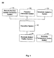
[0042]図1は、システム100の要素が本発明の実施形態においてどのように統合されるかを示す簡略図である。このシステム100には、前駆物質が堆積チャンバ内で基板ウエハ上で化学的に反応し流動性誘電体膜(例えば、酸化シリコン膜)を形成することができる堆積システム102が含まれる。堆積システム102には、堆積チャンバ内部に高周波電力が生じ、プラズマを生成するコイル及び/又は電極が含まれてもよい。プラズマは、前駆物質の反応速度を高めることができ、基板上の流動性誘電物質の堆積速度を上げることができる。
[0042] FIG. 1 is a simplified diagram illustrating how elements of system 100 are integrated in an embodiment of the present invention. The system 100 includes a
[0043]流動性酸化物が堆積されるように、基板運動と位置決めシステム104は、より一様に基板の異なる部分を前駆物質流にさらすために基板を回転させるために用いることができる。このことにより、前駆物質内の化学種の物質移動がより均一になることができる。また、基板の堆積表面の上により幅広く低粘性膜を拡散させることができる。位置決めシステム104には、回転可能で垂直に移動可能な基板ペデスタルが含まれてもよく、結合されてもよい。
[0043] The substrate motion and
[0044]システム100には、また、基板の温度を上下するのに作用可能な基板温度制御システム106が含まれてもよい。温度制御システム106は、基板ペデスタルに結合され、直接接触か又は基板の基板ペデスタルへの他の熱的結合によって基板へ、また、基板から熱を移動することができる。温度システム106は、基板温度を制御する循環流体(例えば、水)、及び/又は物質を通って電流を流すことによって熱エネルギーを供給する電気材料(例えば、抵抗加熱フィラメント)を用いることができる。
[0044] The system 100 may also include a substrate
[0045]流動性誘電体膜を形成するために用いられる前駆物質は、前駆物質分配システム108によって供給することができる。分配システム108の例としては、堆積システム102において堆積チャンバの最上部と側面から前駆物質を流すバッフルシステムとノズルシステムが挙げられる。例としては、また、前駆物質ガスが堆積チャンバ内に分配される複数の開口部を有するシャワーヘッドが挙げられる。追加の例において、システム108には、前駆物質が堆積チャンバへ流れる複数の開口部を有するノズルのないガスリングが含まれてもよい。
[0045] The precursor used to form the flowable dielectric film may be supplied by the
[0046]分配システム108は、堆積チャンバへ二つ以上の前駆物質を独立して流すように構成されてもよい。これらの構成において、少なくとも一対の前駆物質は、それらが堆積チャンバ内で混合し反応するために分配システムを出るまで互いに接触しない。例えば、反応種生成システム110は、原子酸素のような高度に反応性の化学種を生成することができ、これは前駆物質分配システム108から堆積システム102に流れるまで、シリコン含有前駆物質のような他の前駆物質と混合又は反応しない。
[0046] The
[0047]システム100において用いられる前駆物質には、流動性誘電酸化物膜を形成するための前駆物質が含まれてもよい。酸化物膜前駆物質には、ラジカル原子酸素のような反応化学種前駆物質だけでなく、他の酸化前駆物質の中でも酸素分子(O2)、オゾン(O3)、水蒸気、過酸化水素(H2O2)、酸化窒素(例えば、N2O、NO2等)のような他の酸化前駆物質が含まれてもよい。酸化物膜前駆物質としては、また、特に、TMOS、TriMOS、TEOS、OMCTS、HMDS、TMCTR、TMCTS、OMTS、TMS、HMDSOを含む有機シリコン化合物のようなシリコン含有前駆物質が挙げられる。このシリコン含有物質には、また、シラン(SiH4)のような炭素をもたないシリコン化合物が含まれてもよい。堆積した酸化物膜がドープされた酸化物膜である場合には、ドーパント前駆物質、例えば、他のホウ素やリンのドーパントの中でも、TEB、TMB、B2H6、TEPO、PH3、P2H6、TMPが用いられてもよい。膜が誘電体の窒化シリコン又は酸窒化シリコンである場合には、特に、アンモニア、BTBAS、TDMAT、DBEAS、DADBSのような窒素含有前駆物質が用いられてもよい。ある膜堆積については、ハロゲンが、例えば、触媒として用いられてもよい。これらのハロゲン前駆物質としては、塩化水素(HCl)、クロロエチルシランのようなクロロシランが挙げられるのがよい。有機酸(例えば、ギ酸)のような他の酸性化合物が用いられてもよい。これらの堆積前駆物質の全てが、特に、ヘリウム、アルゴン、窒素(N2)、水素(H2)が挙げられるのがよいキャリヤガスによって分配システム108と堆積システム102を通って運搬されてもよい。
[0047] Precursors used in system 100 may include precursors for forming a flowable dielectric oxide film. Oxide film precursors include not only reactive chemical precursors such as radical atomic oxygen, but also oxygen molecules (O 2 ), ozone (O 3 ), water vapor, hydrogen peroxide (H) among other oxidation precursors. 2 O 2 ), nitric oxide (eg, N 2 O, NO 2, etc.) may be included. Oxide film precursors also include silicon-containing precursors such as organosilicon compounds including TMOS, TriMOS, TEOS, OMTS, HMDS, TMCTR, TMCTS, OMTS, TMS, and HMDSO, among others. The silicon-containing material may also include a silicon compound without carbon, such as silane (SiH 4 ). When the deposited oxide film is a doped oxide film, among other dopant precursors, for example, other boron or phosphorus dopants, TEB, TMB, B 2 H 6 , TEPO, PH 3 , P 2 H 6 and TMP may be used. When the film is a dielectric silicon nitride or silicon oxynitride, nitrogen-containing precursors such as ammonia, BTBAS, TDMAT, DBEAS, DADBS may be used, among others. For certain film depositions, halogen may be used as a catalyst, for example. These halogen precursors may include chlorosilanes such as hydrogen chloride (HCl) and chloroethylsilane. Other acidic compounds such as organic acids (eg formic acid) may be used. All of these deposition precursors may be transported through
[0048]このシステム100には、また、基板表面上に堆積した流動性誘電物質を焼成及び/又は硬化することができる基板照射システム112が含まれてもよい。照射システム112には、例えば、誘電物質のシラノール基を酸化シリコンと水に分解することによって膜を硬化するために用いることができるUV光を放出することができる一つ以上のランプが含まれてもよい。照射システムには、水蒸気や他の揮発性化学種を膜から除去するとともにより密度を高くするために流動性膜をベーキング(例えば、アニーリング)用の加熱ランプが含まれてもよい。
[0048] The system 100 may also include a
[0049]ここで図2Aを参照すると、本発明の実施形態による例示的プロセスシステム200の断面が示されている。このシステム200には、前駆物質が化学的に反応し、流動性誘電体膜が基板ウエハ202上に堆積される堆積チャンバ201が含まれる。このウエハ202(例えば、200mm、300mm、400mm径等の半導体基板ウエハ)は、基板202を上に横たわる前駆物質分配システム206により近いか又はより離れて位置決めするように垂直にも移動可能である回転可能な基板ペデスタル204に結合されてもよい。ペデスタルは、約1rpm〜約2000rpm(例えば、約10rpm〜約120rpm)の回転速度で基板ウエハを回転させることができる。ペデスタルは、前駆物質分配システムの側ノズル208から、例えば約0.5mm〜約100mmの距離に基板を垂直に移動することができる。
[0049] Referring now to FIG. 2A, a cross-section of an
[0050]前駆物質分配システム206には、それぞれが二つの異なる長さの一方をもつ複数の放射状分配側ノズル208が含まれる。追加の実施形態(図示せず)において、側ノズルは堆積チャンバの壁の周りに分配された開口部のリングを残すために除かれてもよい。前駆物質は、これらの開口部を通ってチャンバへ流れる。
[0050] The
[0051]分配システム206には、また、基板ペデスタル204の中央と同軸であってもよい円錐状の最上バッフル210が含まれてもよい。流体チャネル212は、バッフルの外側に進む表面を流れる前駆物質よりも前駆物質又はキャリヤガスを異なる組成で供給するためにバッフル210の中央を通ってもよい。
[0051] The
[0052]バッフル210の外側面は、堆積チャンバ201の上に位置決めされる反応種生成システム(図示せず)から反応性前駆物質を進めるコンジット214によってとり囲まれてもよい。コンジット214は、一端がバッフル210の外側面で開いて対向する端が反応種生成システムに結合されている真っすぐな円形チューブであってもよい。
[0052] The outer surface of the
[0053]反応種生成システムは、より安定な出発物質をプラズマにさらすことによって反応種を生成させる遠隔プラズマ生成システム(RPS)であってもよい。例えば、出発物質は、分子酸素(又はオゾン)を含む混合物であるのがよい。この出発物質をRPSからのプラズマにさらすと、分子酸素の一部を原子酸素、非常に低い温度(例えば100℃未満)で有機シリコン前駆物質(例えばOMCTS)と化学的に反応して基板表面上に流動性誘電体を形成する高度に反応性のラジカル種に解離させる。反応種生成システムにおいて生成される反応種がしばしば室温でさえも他の堆積前駆物質と非常に反応性であることから、これらはコンジット214の下の分離したガス混合物内に運搬され、他の堆積前駆物質と混合される前にバッフル210によって反応チャンバ201に分散されてもよい。
[0053] The reactive species generation system may be a remote plasma generation system (RPS) that generates reactive species by exposing more stable starting materials to the plasma. For example, the starting material may be a mixture containing molecular oxygen (or ozone). When this starting material is exposed to plasma from the RPS, some of the molecular oxygen reacts chemically with the organic silicon precursor (eg OMCTS) at a very low temperature (eg less than 100 ° C.) on the substrate surface. To dissociate into highly reactive radical species that form a fluid dielectric. Since the reactive species produced in the reactive species generation system are often very reactive with other deposition precursors, even at room temperature, they are transported into a separate gas mixture under the
[0054]システム200には、また、堆積チャンバ201のドーム216の周巻きつけたrfコイル(図示せず)が含まれてもよい。これらのコイルは、堆積チャンバ201内に誘導結合型プラズマを生成して、反応種前駆物質と他の前駆物質の反応性を更に高めて、基板上に流体誘電体膜を堆積させることができる。例えば、バッフル210によってチャンバに分散された反応性原子酸素とチャネル212及び/又は一つ以上の側ノズル208からの有機シリコン前駆物質を含有するガスフローは、rfコイルによって基板202の上に形成されたプラズマに進められてもよい。原子酸素と有機シリコン前駆物質は低温でさえプラズマ中で急速に反応して、基板表面上に極めて流動性の誘電体膜を形成する。
[0054] The
[0055]基板表面自体は、ペデスタル204によって回転させて、堆積した膜の均一性を高めることができる。回転面は、ウエハ堆積面の面に平行であってもよく、又は二つの面は部分的に整列していなくてもよい。面が整列していない場合、基板204の回転は、堆積表面の上の空間に流体乱流を生成することができる傾きを生じることがある。ある状況において、この乱流は、基板表面上に堆積した誘電体膜の均一性を高めることがある。ペデスタル204には、また、真空チャックを生成して、移動するにつれてペデスタル上の適切な位置にウエハを保持する凹所及び/又は他の構造が含まれてもよい。チャンバ内の典型的な堆積圧力は、約0.05トール〜約200トール合計チャンバ圧(例えば1トール)の範囲であり、適切な位置にウエハを保持するのに適した真空チャックを生成する。
[0055] The substrate surface itself can be rotated by the
[0056]ペデスタルの回転は、堆積チャンバの下に位置決めされ且つペデスタル204を支持するシャフト220に回転して結合されたモータ218によって作動させることができる。シャフト220には、また、冷却流体/電気ワイヤを堆積チャンバ(図示せず)の下の冷却/加熱システムからペデスタル204に運ぶ内部チャネル(図示せず)が含まれてもよい。これらのチャネルは、中央からペデスタルの周辺まで伸長して、上に横たわる基板ウエハ202に均一な冷却及び/又は加熱を与えることができる。これらは、また、シャフト220と基板ペデスタル204が回転し更に/又は移動している場合に作動させるように設計されてもよい。例えば、冷却システムは、ペデスタルを回転させながら流動性酸化物膜の堆積中に基板ウエハ202を100℃未満に保つように作動させることができる。
[0056] The rotation of the pedestal may be actuated by a
[0057]このシステム200には、更に、ドーム216の上に位置決めされた照射システム222が更に含まれてもよい。照射システム222からのランプ(図示せず)は、下に横たわる基板202を照射して、基板上に堆積した膜を焼成又はアニールすることができる。ランプは、また、堆積中に活性化して、膜前駆物質又は堆積した膜における反応を高めることもできる。ドーム216の少なくとも最上部は、ランプから放出された光の一部を伝達することが可能な半透明な物質から製造される。
[0057] The
[0058]図2Bは、側ノズル253の上に位置決めされた貫通プレート252が前駆物質を最上注入口254から分配する例示的処理システム250を示す他の実施形態である。貫通プレート252は、プレートの厚さを横切る複数の開口部260を通って前駆物質を分配する。プレート252は、例えば、約10〜2000個の開口部(例えば、200個の開口部)をもつことができる。図示した実施形態において、貫通プレートは、TMOS又はOMCTSのような原子酸素及び/又は他の酸素含有ガスのような酸化ガスを分配してもよい。図示した構成において、酸化ガスは、堆積基板の上に導入されるシリコン含有前駆物質の上の堆積チャンバに導入される。
[0058] FIG. 2B is another embodiment showing an
[0059]最上注入口254は、二つ以上の前駆物質を混合と反応から貫通プレート252の上の空間に入るまで保つ二つ以上の独立した前駆物質(例えば、ガス)フローチャネル256と258を有してもよい。第一フローチャネル256は、注入口254の中央をとり囲む円環形を有してもよい。このチャネルは、チャネル256の下と貫通プレート252の上の空間に流れる反応種前駆物質を生成する上に横たわる反応種生成ユニット(図示せず)に結合されてもよい。第二フローチャネル258は、円筒形であってもよく、プレート252の上の空間に第二前駆物質を流すために用いてもよい。このフローチャネルは、反応種生成ユニットを迂回する前駆物質及び/又はキャリヤガス源から開始されてもよい。その後、第一前駆物質と第二前駆物質が混合され、プレート252における開口部260を通って下に横たわる堆積チャンバに流れる。
[0059] The
[0060]貫通プレート252と最上注入口254は、堆積チャンバ270内の下に横たわる空間に酸化する前駆物質を分配するために用いられてもよい。例えば、第一フローチャネル256は、原子酸素(基底状態か又は電子的励起状態で)、分子酸素(O2)、N2O、NO、NO2、及び/又はオゾン(O3)の一つ以上を含む酸化する前駆物質を分配するのがよい。酸化する前駆物質には、ヘリウム、アルゴン、窒素(N2)等のキャリヤガスが含まれてもよい。第二のチャネル258は、また、酸化する前駆物質、キャリヤガス、及び/又はアンモニア(NH3)のような追加ガスを分配することもできる。
[0060] The through
[0061]システム250は、堆積チャンバの異なる部分を異なる温度に加熱するように構成されてもよい。例えば、第一ヒータゾーンは、最上リッド262と貫通プレート252を約70℃〜約300℃(例えば、約160℃)の範囲の温度まで加熱するのがよい。第二ヒータゾーンは、第一ヒータゾーン(例えば、300℃以上)と同じか又は異なる温度まで基板ウエハ264とペデスタル266の上の堆積チャンバの側壁を加熱するのがよい。このシステム250は、また、第一及び/又は第二ヒータゾーン(例えば、約70℃〜約120℃)と同じか又は異なる温度まで基板ウエハ264とペデスタル266の下の第三ヒータゾーンを有してもよい。更に、ペデスタル266には、ペデスタルと基板の温度を約-40℃〜約200℃(例えば、約100℃〜約160℃、約100℃未満、約40℃等)に設定するペデスタルシャフト272の内側の加熱及び/又は冷却コンジット(図示せず)が含まれてもよい。処理中、ウエハ264は、リフトピン276でペデスタル266を下げてもよく、スリットバルブドア278の周りに位置してもよい。
[0061] The
[0062]このシステム250には、更に、ウエハエッジ部のプレナム内に及び/又はウエハエッジ部の周りの柱面上に位置し、更に/又はウエハエッジ部の周りに位置した円錐形の表面上に複数の開口部を含むポンピングライナ274(即ち、ポンピングポートの非対称位置を相殺する圧力均等化チャネル)が含まれてもよい。開口部自体は、ライナ274に示したように円形であってもよく、スロット(図示せず)のような異なる形であってもよい。開口部は、直径が、例えば、約0.125インチ〜約0.5インチであってもよい。ウエハが処理される場合、ポンピングライナ274は、基板ウエハ264の上か下にあってもよい。それは、スリットバルブドア278の上に位置してもよい。
[0062] The
[0063]図2Cは、図2Bに示したプロセスシステム250を示す他の断面図である。図2Cは、約10インチ〜約18インチ(例えば、約15インチ)の範囲にある主チャンバ内壁径を含む、システム250のある寸法を示す図である。また、基板ウエハ264と約0.5インチ〜約8インチ(例えば、約5.1インチ)の側ノズルの間の距離を示している。更に、基板ウエハ264と貫通プレート252の間の距離は、約0.75インチ〜約12インチ(例えば、約6.2インチ)の範囲であってもよい。更に、基板ウエハとドーム268の最上内面間の距離は、約1インチ〜約16インチ(例えば、約7.8インチ)であってもよい。
[0063] FIG. 2C is another cross-sectional view of the
[0064]図2Dは、圧力同等化チャネル282とポンピングライナ284を含む堆積チャンバ280の一部を示す断面である。図示した構成において、チャネル282と開口部284は、上に横たわるシャワーヘッド、最上バッフル及び/又は側ノズルの下に、基板ペデスタル286とウエハ288と同じ高さか又はそれらの上に位置してもよい。
[0064] FIG. 2D is a cross section illustrating a portion of a
[0065]チャネル282と開口部284は、チャンバにおける非対称の圧力作用を減少させることができる。これらの作用は、堆積チャンバ280内に圧力勾配を生じ得るポンピングポートの非対称の場所によって引き起こされることがある。例えば、基板ペデスタル286及び/又は基板ウエハ288の下の圧力勾配はペデスタルとウエハを傾けさせることがあり、誘電体膜の堆積において凹凸を生じることがある。チャネル282とポンピングライナ開口部284は、チャンバ280における圧力勾配を減少させ、堆積中にペデスタル286とウエハ288の位置を安定させるのを援助する。
[0065]
[0066]図3Aは、上の部分がコンジット214によってとり囲まれているバッフル210の中央に形成されたチャネル212を含む、図2Aにおける前駆物質分配システム206の最上部302を示す実施形態の図である。図3Aは、コンジット214を下にバッフル210の外面の上を流れる反応種前駆物質304を示している。反応種前駆物質304が堆積チャンバへ最も近づくバッフル210の円錐状の末端に達するにつれて、チャンバへ放射状に分配され、そこで反応種304が第二前駆物質306と最初に接触する。
[0066] FIG. 3A is an illustration of an embodiment showing the top 302 of the
[0067]第二前駆物質306は、有機シラン前駆物質であるのがよく、キャリヤガスを含んでもよい。有機シラン前駆物質としては、他の前駆物質の中でも、TMOS、TriMOS、TEOS、OMCTS、HMDS、TMCTR、TMCTS、OMTS、TMS、及びHMDSOのような一つ以上の化合物が挙げられるのがよい。キャリヤガスとしては、他のキャリヤガスの中でも、窒素(N2)、水素(H2)、ヘリウム、アルゴンのような一つ以上のガスが挙げられるのがよい。前駆物質は、前駆物質供給ライン308に接続され、チャネル212にも結合されている供給源(図示せず)から送り込まれる。第二前駆物質306は、バッフル210の外側面の上を流れる反応種304にさらされずに中央チャネル212を下に流れることができる。第二前駆物質304がバッフル210の底を出て堆積チャンバに入るときに、側ノズル208によって供給される反応種304と追加の前駆物質と第一時間混合することができる。
[0067] The
[0068]コンジット214を下に流れる反応性前駆物質304は、RPSユニットのような反応種生成ユニット(図示せず)において生成される。例えば、RPSユニットは、反応種を形成するのによく適したプラズマ条件を生じ得る。RPSユニットにおけるプラズマは堆積チャンバ内で生成されるプラズマから離れていることから、異なるプラズマ条件をそれぞれの要素に使用し得る。例えば、O2、O3、N2O等の酸素前駆物質から原子酸素ラジカルを形成するためのRPSユニットにおけるプラズマ条件(例えば、rf電力、rf周波数、圧力、温度、キャリヤガス分圧等)は、原子酸素が一つ以上のシリコン含有前駆物質(例えば、TMOS、TriMOS、OMCTS等)と反応し且つ下に横たわる基板上に流動性誘電体膜を形成する堆積チャンバ内のプラズマ条件とは異なってもよい。
[0068] The
[0069]図3Aは、第一及び第二前駆物質が堆積チャンバに達するまで互いに独立した第一前駆物質と第二前駆物質の流れを保つように設計されたデュアルチャネル最上バッフルを示す図である。本発明の実施形態には、また、チャンバへ三つ以上の前駆物質の独立した流れの構成が含まれる。例えば、構成には、バッフル210を通って内部を流れるチャネル212のような二つ以上の独立したチャネルが含まれてもよい。これらのチャネルのそれぞれは、堆積チャンバに達するまで互いに独立して流れる前駆物質を運ぶことができる。追加の例としては、その中央を通って流れるチャネルがない単一チャネルバッフル210が挙げられてもよい。これらの実施形態において、第二前駆物質306は、側ノズル208から堆積チャンバに入り、バッフル210によってチャンバに放射状に分配された反応性前駆物質304と反応する。
[0069] FIG. 3A shows a dual channel top baffle designed to keep the first and second precursor flows independent of each other until the first and second precursors reach the deposition chamber. . Embodiments of the present invention also include an independent flow configuration of three or more precursors into the chamber. For example, a configuration may include two or more independent channels, such as
[0070]図3Bと図3Cはバッフル210の追加の実施形態を示す図である。図3Bと図3Cにおいて、チャネル212は、貫通プレート310a-310bによって下側(即ち、堆積チャンバに最も近い側)に画成された円錐状の容積に開放している。前駆物質は貫通プレートにおける開口部312を通ってこの容積を出る。図3Bと図3Cは、側壁と底プレート310a-310bの間の角度がどのように変動し得るかを示す図である。図は、また、前駆物質が堆積チャンバに入るにつれて流れる円錐外面の形の態様を示している。
[0070] FIGS. 3B and 3C illustrate additional embodiments of the
[0071]図3Dは、堆積チャンバの最上部から前駆物質を分配する最上バッフルの代わりに用いられる最上注入口314と貫通プレート316の構成を示す図である。図示した実施形態において、最上注入口314は、二つ以上の前駆物質を貫通プレート316の上の空間に入るまで混合と反応から保持する二つ以上の独立した前駆物質フローチャネル318と320を有してもよい。第一フローチャネル318は、注入口314の中央をとり囲む円環形を有してもよい。このチャネルは、チャネル318を下に貫通プレート316の上の空間に流れる反応種前駆物質を生成する上に横たわる反応種生成ユニット322に結合されてもよい。第二フローチャネル320は、円筒形であってもよく、プレート316の上の空間に第二前駆物質を流すために用いられてもよい。このフローチャネルは、反応種生成ユニットを迂回する前駆物質及び/又はキャリヤガス源から開始してもよい。その後、第一前駆物質と第二前駆物質が混合され、プレート316における開口部324を通って下に横たわる堆積チャンバに流れる。
[0071] FIG. 3D shows the configuration of the
[0072]図3Eは、本発明の実施形態による最上貫通プレート356を含むプロセスシステム350において酸素含有前駆物質352とシリコン含有前駆物質354の前駆物質流分配を示す図である。図3Dのように、ラジカル原子酸素のような酸素含有ガスは遠隔プラズマシステム(図示せず)によって生成され、堆積チャンバの最上部を通って貫通プレート356の上の空間に導入される。その後、反応性酸素種は貫通プレート356における開口部358を通ってシリコン含有物質354(例えば、有機シラン及び/又はシラノール前駆物質)が側ノズル360によってチャンバに導入されるチャンバの領域に下に流れる。
[0072] FIG. 3E is a diagram illustrating precursor flow distribution of an oxygen-containing
[0073]図3Eに示される側ノズル360は、堆積チャンバに伸長するこれらの遠位端でキャップされている。シリコン含有前駆物質は、ノズルコンジットの側壁に形成された複数の開口部362を通って側ノズル360を出る。これらの開口部362は、基板ウエハ364に面するノズル側壁の部分に形成されて、シリコン含有物質354の流れをウエハに進めることができる。開口部362は、同じ方向に前駆物質354の流れを進めるように共に直線的に整列されてもよく、又は側壁に沿って異なる放射状位置に形成されて、前駆物質流を下に横たわるウエハ対して異なる角度で進めることができる。キャップされた側ノズル360の実施形態には、直径が約8ミル〜200ミル(例えば、約20ミル〜約80ミル)の開口部362と、約40ミル〜約2インチ(例えば、0.25インチ〜1インチ)の開口部間の間隔が含まれる。開口部の数は開口部及び/又は側ノズルの長さの間の間隔に対して変動してもよい。
[0073] The side nozzles 360 shown in FIG. 3E are capped at their distal ends that extend into the deposition chamber. The silicon-containing precursor exits the
[0074]図4Aは、発明の実施形態によるプロセスシステムにおける側ノズルの構成を示す正面図である。図示した実施形態において、側ノズルは三つのノズルのグループに堆積チャンバの周りに放射状に分配され、中央ノズル402は二つの隣接したノズル404よりも堆積チャンバ内に更に伸長している。これらの三グループの十六個が、合計48個の側ノズルについて、堆積チャンバの周りに均一に分配される。追加の実施形態には、約12〜約80個のノズルの範囲にあるノズルの総数が含まれる。
[0074] FIG. 4A is a front view illustrating the configuration of a side nozzle in a process system according to an embodiment of the invention. In the illustrated embodiment, the side nozzles are distributed radially around the deposition chamber into groups of three nozzles, and the
[0075]ノズル402と404は、基板ウエハの堆積面の上に隔置されてもよい。基板とノズルの間の間隔は、例えば、約1mm〜約80mm(例えば、約10mm〜約30mmの範囲)の範囲にあってもよい。ノズル402と404と基板との間のこの距離は、堆積中変動してもよい(例えば、堆積中、ウエハを垂直に移動してもよいだけでなく、回転及び/又撹拌してもよい)。
[0075] The
[0076]ノズル402と404は、全て同一プレートに配置されてもよく、又は異なる設定のノズルが異なるプレートに位置してもよい。ノズル402と4040は、ウエハの堆積表面に平行な中心線に向けられてもよく、基板表面に対して上向き又は下向きに傾けられてもよい。
[0076] The
[0077]ノズル402と404は、堆積チャンバに伸長する遠位端とノズルに前駆物質を供給するアニュラ型ガスリング406の内径表面に結合した近位端を有する。ガスリングは、例えば、約10インチ〜約22インチ(約14インチ〜約18インチ、約15インチ等)の範囲にある内径を有してもよい。ある構成において、より長いノズル402の遠位端は下に横たわる基板の周辺を超えて基板の内部の上の空間に伸長し、より短いノズル404の末端は基板周辺に達しない。図4に示される実施形態において、より短いノズル404の遠位先端は直径12インチ(即ち、300mm)の基板ウエハの周辺にまで伸長し、より長いノズル402の遠位先端は堆積表面の内部より更に4インチ伸長する。
[0077] Nozzles 402 and 404 have a distal end that extends into the deposition chamber and a proximal end that is coupled to the inner diameter surface of an
[0078]ガスリング406は、前駆物質をノズル402と404に供給する一つ以上の内部チャネル(例えば、2〜4つのチャネル)を有してもよい。単一チャネルガスリングについて、内部チャネルは、全ての側ノズル402と404に前駆物質を供給してもよい。デュアルチャネルガスリングについては、一つのチャネルはより長いノズル402に前駆物質を供給してもよく、第二チャネルはより短いノズル404に前駆物質を供給する。それぞれのチャネルについて、反応性堆積前駆物質(例えば、有機シラン前駆物質の種類)及び/又は分圧、キャリヤガスの流量の種類は、堆積法によっては同じであっても異なってもよい。
[0078] The
[0079]図4Bは、本発明の実施形態よるプロセスシステムにおけるキャップされた側ノズル410の構成を示す図である。上記図3Eに示される側ノズル360と同様に、ノズル410は堆積チャンバに伸長する遠位端でキャップされる。ノズルを通って流れる前駆物質は、ノズルコンジットの側壁に形成される複数の開口部412を通って出る。これらの開口部412は基板ウエハ(図示せず)に面するノズル側壁の一部に形成されて、ウエハに向かって前駆物質の流れを進めることができる。開口部412は共に直線的に整列して、同じ方向に前駆物質流を進めることができ、又は側壁に沿って異なる放射状の位置に形成されて、下に横たわるウエハに対して異なる角度で前駆物質流を進めることができる。
[0079] FIG. 4B is a diagram illustrating a configuration of a capped
[0080]ノズル410は、ノズル410の隣接した末端が結合される環状ガスリング414によって送り込まれてもよい。全てのノズル410に前駆物質を供給するためにガスリング414が単一ガスフローチャネル(図示せず)を有してもよく、又はノズル410の二つ以上の設定を供給するためにリングが複数のガスフローチャネルを有してもよい。例えば、デュアルチャネルガスリング設計において、第一チャネルは第一前駆物質(例えば、第一有機シラン前駆物質)を第一組のノズル410(例えば、図4Bに示されたノズルのより長い設定)に供給することができ、第二のチャネルは第二前駆物質(例えば、第二有機シラン前駆物質)を第二組のノズル410(例えば、図4Bに示されたより短い組のノズル)に供給することができる。
[0080] The
[0081]図4Cは、図4Bに示されるような側ノズル420を通る前駆物質流の断面図を示す図である。前駆物質418(例えば、蒸気分配システムからのキャリヤガスにおける有機シラン蒸気前駆物質)は、側ノズル420の近接端に結合した前駆物質フローチャネル416によって供給される。前駆物質418はノズルコンジットの中央を通って流れ、側壁内の開口部422を出る。図示したノズル構成において、開口部422は下向きに整列して、下に横たわるウエハ基板(図示せず)に向かって前駆物質418流を進ませる。開口部422は、直径が約8ミル〜約200ミル(例えば、約20ミル〜約80ミル)であり、開口部間の間隔が約40ミル〜約2インチ(例えば、約0.25インチ〜約1インチ)である。開口部422の数は、開口部間の間隔及び/又は側ノズル420の長さに対して変動してもよい。
[0081] FIG. 4C shows a cross-sectional view of the precursor flow through the
[0082]本発明の実施形態には、また、図4Bに示される一組の放射側ノズルの代わりに用いられる単一片放射前駆物質マニホールドが含まれてもよい。(シャワーヘッドと呼ばれてもよい)この前駆物質マニホールド450の実施形態の図は、図4Dに示される。マニホールド450には、前駆物質外部リング454の周りに放射状に分配される複数の矩形コンジット452が含まれる。コンジット452の近接端は外部リング454に結合されてもよく、コンジット452の遠位端はアニュラ型内部リング456に結合される。アニュラ型内部リング456は、また、複数の内部コンジット458の近接端に結合されてもよく、その遠位端はアニュラ型中央リング460に結合されてもよい。
[0082] Embodiments of the present invention may also include a single piece radiation precursor manifold used in place of the set of radiation nozzles shown in FIG. 4B. An illustration of this
[0083]矩形コンジット452は、前駆物質外部リング454内の一つ以上の前駆物質チャネル(図示せず)によって前駆物質(例えば、一つ以上の有機シリコン前駆物質)で供給されてもよい。前駆物質は、コンジットの側面に形成された複数の開口部462を通ってコンジット452を出る。開口部462の直径は、約8ミル〜200ミル(例えば、約20ミル〜約80ミル)であり、開口部間の間隔は、約40ミル〜約2インチ(例えば、約0.25インチ〜約1インチ)である。開口部462の数は、開口部間の間隔及び/又はコンジット452の長さに対して変動してもよい。
[0083] The
[0084]図4Eは、図4Dに示される前駆物質分配マニホールドの拡大部分を示す図である。図示された実施形態において、放射状に分配されたコンジット452a-452bには、長さがアニュラ型内部リング456まで伸長し、第一組のコンジット452aが含まれてもよく、長さが内部リング456を超えてアニュラ型中央リング460まで伸長する第二組のコンジット452bが含まれてもよい。第一組と第二組のコンジット452は前駆物質の異なる混合物で供給されてもよい。
[0084] FIG. 4E shows an enlarged portion of the precursor distribution manifold shown in FIG. 4D. In the illustrated embodiment, the radially distributed
[0085]上述したように、堆積システムの実施形態には、また、基板上に堆積した流動性誘電体膜を硬化し更に/又は加熱する照射システムが含まれてもよい。図5A及び図5Bは、このような一照射システム500のような実施形態を示す図であり、半透明なドームの上に位置決めされ且つ下に横たわる基板506を照射するのに作用可能な同心系の環状ランプ502が含まれる。ランプ502は、反射ソケットに埋め込まれてもよく、ランプの側面は基板506に向かってランプが放出するより高く進ませる反射コーティングをもつ。ランプ502の総数は、単一ランプから、例えば、10ランプまで変動してもよい。
[0085] As described above, embodiments of the deposition system may also include an irradiation system that cures and / or heats the flowable dielectric film deposited on the substrate. FIGS. 5A and 5B illustrate such an embodiment of one
[0086]ランプ502には、硬化プロセスの場合にはUV放出ランプ及び/又はアニールプロセスの場合にはIR放出ランプが含まれてもよい。例えば、ランプ502は、水平フィラメント(即ち、ランプの電球の対称軸に垂直に向けられたフィラメント)、垂直フィラメント(即ち、電球の対称軸に平行に向けられたフィラメント)、及び/又は円形フィラメントを有してもよいタングステンハロゲンランプであるのがよい。反射ソケット508の異なるランプ502は、異なるフィラメント構成を有してもよい。
[0086] The
[0087]ランプ502からの光は、ドームを通って基板堆積面に伝達される。ドーム504の少なくとも一部には、UV及び/又は熱放射を堆積チャンバに通過させることを可能にする光学的に透明な窓510が含まれてもよい。窓510は、例えば、石英、溶融石英、酸窒化アルミニウム、又は他の適した半透明物質から製造されるのがよい。図5A-図5Fに示されるように、窓510は、形が環状でドーム504の最上部を覆ってもよく、直径が、例えば、約8インチ〜約22インチ(例えば、約14インチ)であってもよい。窓510の中央には、コンジットを堆積チャンバの上部に通過させることを可能にする内部開口部が含まれてもよい。内部開口部の直径は、例えば、約0.5インチ〜約4インチ(例えば、直径約1インチ)であってもよい。
[0087] Light from
[0088]図5Cと図5Dは、環状の代わりに真っすぐな環状電球を有するランプ512の他の構成を示す図である。真っすぐなランプ512は平行に整列されてもよく、ドーム504の半透明な窓510の上に位置決めされた反射ソケット514に埋め込まれてもよい。反射ソケット514は、円環形であってもよく、下に横たわる窓510の直径に一致してもよい。ランプ512の末端は、ソケット514の周辺を超えて伸長してもよい。窓510の中央の両側面のランプ512の数は等しく、約4以上のランプ(約4〜約10個のランプ)が用いられてもよい。
[0088] FIGS. 5C and 5D illustrate another configuration of a
[0089]図5Eと図5Fは、窓510の中央の周りの対向する側に位置決めされた二つの大きいランプ516を有する照射システムの他の構成を示す図である。大きいランプは、互いに並行に、又は平行より小さい角度で整列されるのがよい。ランプ516は、また、ランプ光の一部を堆積チャンバ内の基板に向かって進ませるのに援助する反射ソケット518に埋め込まれてもよい。
[0089] FIGS. 5E and 5F illustrate another configuration of an illumination system having two
[0090]図5A-図5Fに示される照射システムの実施形態は、基板表面上の堆積中及び/又は堆積後に流動性誘電体膜を照射するために用いることができる。また、堆積ステップ(例えば、パルスアニール)の間に基板を照射するために用いることができる。膜堆積中、ウエハは、温度制御ペデスタル上に位置決めされる。ウエハ温度は、例えば、約-40℃〜約200℃(例えば、40℃)に設定されるのがよい。基板がベーキング(即ち、アニーリング)プロセス中に照射される場合、ウエハの温度は約1000℃まで上昇してもよい。この高温アニールプロセス中、基板ペデスタル上のリフトピンはペデスタルから基板を持ち上げることができる。このことは、ペデスタルがヒート・シンクとして作用することから防止するとともにウエハ温度がより速い速度(例えば、約100℃/秒まで)で増加することを可能にする。 [0090] The embodiment of the illumination system shown in FIGS. 5A-5F can be used to irradiate the flowable dielectric film during and / or after deposition on the substrate surface. It can also be used to irradiate the substrate during a deposition step (eg, pulse annealing). During film deposition, the wafer is positioned on the temperature control pedestal. The wafer temperature may be set to about −40 ° C. to about 200 ° C. (for example, 40 ° C.), for example. If the substrate is irradiated during the baking (ie, annealing) process, the temperature of the wafer may rise to about 1000 ° C. During this high temperature annealing process, lift pins on the substrate pedestal can lift the substrate from the pedestal. This prevents the pedestal from acting as a heat sink and allows the wafer temperature to increase at a faster rate (eg, up to about 100 ° C./second).
[0091]堆積システムの実施形態は、集積回路チップを製造するより大きな製造システムに組み込むことができる。図6は、本発明の実施形態による、堆積チャンバ、ベーキングチャンバ、硬化チャンバのこのような一システム600を示す図である。図面において、一組のFOOP602は、ロボットアーム604によって受け取り、ウエハ処理チャンバ608a-608fの一つに配置される前に低圧保持領域606に配置される基板ウエハ(例えば、300mm径ウエハ)を供給する。第二ロボットアーム610は、基板ウエハを保持領域606から処理チャンバ608a-608fにとその逆に搬送するために用いることができる。
[0091] Embodiments of deposition systems can be incorporated into larger manufacturing systems that manufacture integrated circuit chips. FIG. 6 is a diagram illustrating one
[0092]プロセスチャンバ608a-608fには、基板ウエハ上に流動性誘電体膜を堆積、アニーリング、硬化及び/又はエッチングするための一つ以上のシステム要素が含まれてもよい。一構成において、二組の処理チャンバ(例えば、608c-608dと608e-608f)は、基板上に流動性誘電体膜を堆積するために用いることができ、第三組の処理チャンバ(例えば、608a-608b)は、堆積した誘電体をアニールするために用いることができる。他の構成において、同じ二組の処理チャンバ(例えば、608c-608dと608e-608f)は、基板上に流動性誘電体膜を堆積し且つアニールするために構成されてもよく、第三組の処理チャンバ(例えば、608a-608b)は堆積した膜のUV又はEビーム硬化に用いられてもよい。更に他の構成において、全て三組のチャンバ(例えば、608a-608f)は、基板上の流動性誘電体膜を堆積し硬化するように構成されてもよい。更に他の構成において、二組のプロセスチャンバ(例えば、608c-608dと608e-608f)は、流動性誘電体の堆積且つUV又はEビーム硬化に用いられてもよく、第三組のプロセスチャンバ(例えば、608a-608b)は、誘電体膜をアニールするのに用いてもよい。流動性誘電体膜の堆積チャンバ、アニーリングチャンバ、効果チャンバの追加の構成がシステム600によって企図されることは理解される。
[0092] The
[0093]更に、一つ以上のプロセスチャンバ608a-608fは、湿式処理チャンバとして構成されてもよい。これらのプロセスチャンバは、流動性誘電体膜を、水分を含む大気中で加熱すること含む。従って、システム600の実施形態には、堆積した誘電体膜上で湿式アニールと乾式アニールの双方を行う湿式処理チャンバ608a-608bとアニール処理チャンバ608c-608dが含まれてもよい。
[0093] Further, one or more of the
シャワーヘッドの設計
[0094]本発明の実施形態によるガス分配とプラズマ生成システムの実施形態には、前駆物質を堆積チャンバへ分配するシャワーヘッドが含まれるのがよい。これらのシャワーヘッドは、二つ以上の前駆物質が堆積チャンバ内で混合するまで接触せずに独立してシャワーヘッドに流れることができるように設計されるのがよい。シャワーヘッドは、また、プラズマがフェースプレートの後ろだけでなく堆積チャンバ内に独立して生成することができるように設計されてもよい。シャワーヘッドのブロッカープレートとフェースプレートの間に生成される独立したプラズマは、反応性前駆物質種を形成するだけでなく、フェースプレートに近い洗浄化学種を活性化することによってシャワーヘッド洗浄プロセスの効率を改善するために用いることができる。二つ以上の前駆物質を堆積領域に独立して流れるように設計されたシャワーヘッドについての詳細は、更に、2005年1月22日出願の“MIXINGENERGIZED AND NON-ENERGIZED GASES FORbSILICONNITRIDE DEPOSITION”と称するJungらによる米国特許出願第11/040,712号に見出すことができ、この全体の内容は全てのために本願明細書に含まれるものとする。
Shower head design
[0094] Embodiments of the gas distribution and plasma generation system according to embodiments of the present invention may include a showerhead that distributes the precursor to the deposition chamber. These showerheads should be designed so that two or more precursors can flow independently to the showerhead without contact until mixed in the deposition chamber. The showerhead may also be designed so that the plasma can be generated independently in the deposition chamber as well as behind the faceplate. The independent plasma generated between the showerhead blocker plate and the faceplate not only forms reactive precursor species, but also activates the cleaning species close to the faceplate, thereby increasing the efficiency of the showerhead cleaning process. Can be used to improve. More details on showerheads designed to flow two or more precursors independently into the deposition area can be found in Jung et al. No. 11 / 040,712, the entire contents of which are hereby incorporated by reference in their entirety.
[0095]ここで図7Aを参照すると、シャワーヘッドシステム700の簡略断面図が示されている。シャワーヘッド700は、二つの前駆物質注入ポート702と704と構成されている。第一前駆物質注入ポート702は、シャワーヘッドの中央と同軸であり、シャワーヘッドの中央を下に、その後、フェースプレート706の後ろに横方向に第一前駆物質の流路を画成する。
[0095] Referring now to FIG. 7A, a simplified cross-sectional view of a
[0096]第二前駆物質注入ポート704は、第一ポート702の周りでガスボックス710とフェースプレート706の間の領域708に第二前駆物質を流すように構成されてもよい。その後、第二前駆物質を、堆積領域712に達する前にフェースプレート706における選ばれた開口部を通って領域708から流すことができる。図7Aに示されるように、フェースプレート706は二組の開口部:領域708と堆積領域の間で流体が連通する一組の開口部と、第一注入ポート702とフェースプレートギャップ718と堆積領域712との間で流体が連通する第二組の開口部716を有する。
[0096] The second
[0097]フェースプレート706は、第一前駆物質と第二前駆物質が堆積領域のシャワーヘッドに残るまで独立して保持するデュアルチャネルフェースプレートであってもよい。例えば、第一前駆物質は、開口部716を通ってシャワーヘッドを出る前にフェースプレートギャップ718内の開口部714の周りに進むことができる。円筒状ポートのようなバリヤは、開口部714をとり囲み、第一前駆物質がこれらの開口部を通って出ることを防止することができる。同様に、開口部714を通って進む第二前駆物質は、フェースプレートギャップ718全体に第二開口部716を出て堆積領域に流れることができない。
[0097] The
[0098]前駆物質がそれぞれ組の開口部を出る場合に、基板ウエハ722と基板ペデスタル724の上の堆積領域712内で混合することができる。フェースプレート706とペデスタル724は、電極を形成して、基板722の上の堆積領域内で容量結合プラズマ726を生成させることができる。
[0098] As the precursors each exit the set of openings, they can be mixed within the
[0099]システム700は、また、フェースプレートの後ろの領域708の後ろに第二プラズマ728を生成するように構成されてもよい。図7Bに示されるように、このプラズマ728は、プラズマのための電極を形成する、ガスボックス710とフェースプレート706間にrf電界を印加することによって生成することができる。このプラズマは、第二前駆物質注入ポート704から領域708へ流れる第二前駆物質から生成されてもよい。第二プラズマ728は、第二前駆混合物において前駆物質の一つ以上から反応種を生成するために用いることができる。例えば、第二前駆物質には、プラズマ728中でラジカル原子酸素種を形成する酸素含有源が含まれてもよい。その後、反応性原子酸素は混合し且つ第一前駆物質(例えば、有機シラン前駆物質)と反応することができる堆積領域にフェースプレート開口部714を通って流れ込むことができる。
[0099] The
[0100]図7Bにおいて、フェースプレート706は、堆積領域内の第二プラズマ728と第一プラズマ726双方の電極として作用することができる。このデュアルゾーンプラズマシステムは、フェースプレート706の後ろに前駆物質反応種を生成するとともにプラズマ中でその反応種と他の前駆物質との反応性を高めるために同時プラズマを用いることができる。更に、プラズマ728は、洗浄前駆物質を活性化してシャワーヘッド開口部内に蓄積した物質とより反応性にするために使用し得る。更に、堆積領域の代わりにシャワーヘッド内で反応種を生成することにより、洗浄活性種と堆積チャンバの壁の間での望ましくない反応の数を減少させることができる。例えば、フェースプレート706の後ろに生成されるより活性のフッ素種は、堆積領域内へ出る前に反応し、それらは堆積チャンバのアルミニウム要素に移動するとともに望ましくないAlF3を形成し得る。
[0100] In FIG. 7B, the
[0101]図8Aと図8Cは、二つの前駆物質混合物が堆積領域に達する前に独立して流れることができるフェースプレート802における第一組の開口部と第二組の開口部804と806の二つの構成を示す図である。図8Aは、第一組の開口部804が第一前駆物質を真っ直ぐなコンジットを通過させ、第二組の開口部806が第二前駆物質を第一開口部をとり囲んでいる同心アニュラ型リング開口部を通過させる、同心開口設計の断面を示す図である。第一前駆物質と第二前駆物質は、フェースプレートと第一混合物の後ろで互いに分離し、堆積領域内の開口部804と806から現れるときに反応する。
[0101] FIGS. 8A and 8C illustrate a first set of openings and a second set of
[0102]図8Bは、フェースプレート表面内に形成された第一開口部と第二開口部804、806のアレイを示すフェースプレート802の一部の図である。第二環状開口部806は、最外フェースプレート層と、第一開口部804を画成するチュブラー壁との間のギャップによって形成される。図に示される実施形態において、環状ギャップ開口部806は中央開口部804の壁の周りの約0.003インチであり、直径が約0.028インチである。第一開口部と第二開口部の他の大きさが用いられてもよいことは当然のことである。第二前駆物質は、これらの環状開口部806を通過し、中央開口部804から現れる前駆物質をとり囲む。
[0102] FIG. 8B is a diagram of a portion of
[0103]図8Cは、第一組の開口部808がなお第一前駆物質の真っ直ぐなコンジットを生成し、第二組の平行な隣接開口部810が第二前駆物質の独立したフローチャネルを与える平行開口設計の断面を示す図である。第一前駆物質と第二前駆物質が混合せず、反応領域にシャワーヘッドを出るまで反応しないように二組の開口部は互いに分離される。
[0103] FIG. 8C shows that the first set of openings 808 still produce straight conduits of the first precursor, and the second set of parallel
[0104]開口部810を出る第二前駆物質は、図8Dに示されるようにシャワーヘッドのエッジ領域から中央に流れることができる。第二前駆物質源と開口部810間に形成されるチャネルは、領域812から開口部808を通って堆積領域へ流れる第一前駆物質から流体的に分離される。第二前駆物質は、複数のシャワーヘッドの中に及び/又は周りに形成される一つ以上の流体チャネルによって供給することができる。
[0104] The second precursor exiting the
[0105]ある範囲の値が示される場合、それぞれの介在値は、特に明らかに影響されない限り、その範囲の上限と下限の間で下限の単位の1/10まで詳しく開示されることは理解される。記載されたあらゆる値又は記載された範囲の介在値と記載された他のあらゆる値又は記載されたその範囲の介在値の間のそれぞれのより小さい範囲が本発明の範囲に包含される。これらのより小さい範囲の上限と下限は独立して範囲に含むか又は除外することができ、記載された範囲の詳しく除外されたあらゆる限度を条件として、いずれか、いずれでもないか又は両方の限度が含まれるそれぞれの範囲も本発明の範囲に包含される。記載された範囲が一方又は両方の限度を含む場合、それらの含まれた限度のいずれか又は両方を除外する範囲も本発明に含まれる。 [0105] When a range of values is indicated, it is understood that each intervening value is disclosed in detail up to 1/10 of the lower limit unit between the upper and lower limits of the range, unless specifically affected. The Each smaller range between any stated value or stated intervening value of a range and any other stated value or intervening value of that range is encompassed within the scope of the invention. The upper and lower limits of these smaller ranges may be independently included or excluded from the range, subject to any specifically excluded limits in the stated range, either, neither or both Each range including is also included in the scope of the present invention. Where the stated range includes one or both of the limits, ranges excluding either or both of those included limits are also included in the invention.
[0106]本明細書に用いられ、また、添えられた特許請求の範囲において、特に明らかに影響されない限り、単数形は、複数の対象を包含する。従って、例えば、“プロセス”について述べることは、複数のこのようなプロセスが含まれてもよく、“ノズル”について述べることは、一つ以上のノズル及び当業者に既知のその等価物等について述べることが含まれてもよい。 [0106] As used herein and in the appended claims, the singular forms include the plural objects unless the context clearly dictates otherwise. Thus, for example, reference to “a process” may include a plurality of such processes, and a description of “nozzle” refers to one or more nozzles and equivalents known to those skilled in the art, etc. May be included.
[0107]また、本明細書と以下の特許請求の範囲に用いられる語“備える”、“含む”は記載された特徴、整数、成分、又はステップの存在を特定するものであるが、一つ以上の他の特徴、整数、成分、ステップ、又は基の存在又は追加を除外しない。 [0107] Also, as used in this specification and the following claims, the terms "comprising" and "including" specify the presence of a described feature, integer, ingredient, or step, The presence or addition of other features, integers, components, steps, or groups are not excluded.
100…システム、200…処理システム、201…堆積チャンバ、202…基板ウエハ、204…ペデスタル、206…分配システム、208…側ノズル、210…バッフル、212…流体チャネル、214…コンジット、216…ドーム、220…シャフト、222…照射システム、250…処理システム、252…貫通プレート、254…注入口、256…フローチャネル、258…フローチャネル、260…開口部、262…リッド、264…基板ウエハ、266…ペデスタル、270…堆積チャンバ、272…ペデスタルシャフト、274…ポンピングライナ、276…リフトピン、278…スリットバルブドア、280…堆積チャンバ、282…チャネル、284…開口部、286…基板ペデスタル、288…ウエハ、304…前駆物質、306…前駆物質、308…前駆物質供給ライン、310…貫通プレート、312…開口部、314…注入口、316…貫通プレート、318…チャネル、320…チャネル、322…反応種生成ユニット、324…開口部、350…プロセスシステム、354…前駆物質、356…貫通プレート、358…開口部、360…側ノズル、362…開口部、364…基板ウエハ、402…ノズル、404…ノズル、406…ガスリング、410…ノズル、412…開口部、414…アニュラ型ガスリング、418…前駆物質、422…開口部、450…マニホールド、452…コンジット、456…リング、462…開口部、502…ランプ、508…ソケット、510…窓、512…ランプ、514…ソケット、516…ランプ、518…ソケット、600…システム、606…保持領域、608…処理チャンバ、700…シャワーヘッドシステム、702…注入ポート、704……貫通プレート、706…フェースプレート、708…領域、710…ガスボックス、712…堆積領域、714…開口部、718…フェースプレートギャップ、726…プラズマ、728…プラズマ、802…フェースプレート、804…開口部、806…開口部、808…開口部、810…開口部。
DESCRIPTION OF SYMBOLS 100 ... System, 200 ... Processing system, 201 ... Deposition chamber, 202 ... Substrate wafer, 204 ... Pedestal, 206 ... Dispensing system, 208 ... Side nozzle, 210 ... Baffle, 212 ... Fluid channel, 214 ... Conduit, 216 ... Dome, 220 ...
Claims (22)
堆積領域、および、ガスボックスとフェースプレートとの間の領域を含む、堆積チャンバと;
該基板を保持する該堆積チャンバ内の基板台と;
-40℃〜200℃の温度で該基板台を維持するようになっている温度制御システムと;
該堆積チャンバに結合した遠隔プラズマ生成システムであって、該プラズマ生成システムが、反応性ラジカルを含む第一誘電前駆物質を生成するために用いられる、前記遠隔プラズマ生成システムと;
該基板台と堆積領域の上であって、該ガスボックスと該フェースプレートとの間の該領域の下に位置決めされたデュアルチャネルシャワーヘッドを備える前駆物質分配システムであって、該シャワーヘッドが、該反応性ラジカルを含む該第一誘電前駆物質が該堆積チャンバに入る第一組の開口部と、第二誘電前駆物質が該堆積チャンバに入る第二組の開口部とを備え、該前駆物質が該堆積領域に入るまで混合されない、前記前駆物質分配システム。 A system for forming a flowable dielectric layer on a substrate from a plasma of a dielectric precursor, comprising:
A deposition chamber including a deposition region and a region between the gas box and the faceplate ;
A substrate platform in the deposition chamber for holding the substrate;
A temperature control system adapted to maintain the substrate platform at a temperature between -40 ° C and 200 ° C;
A remote plasma generation system coupled to the deposition chamber, wherein the plasma generation system is used to generate a first dielectric precursor containing reactive radicals;
A precursor distribution system comprising a dual channel showerhead positioned above the substrate stage and deposition region and below the region between the gas box and the faceplate , the showerhead comprising: comprising a first set of openings said first dielectric precursor comprising the reactive radicals from entering into the deposition chamber, and a second set of openings second dielectric precursor enters the deposition chamber, the precursor The precursor distribution system, wherein the precursor distribution system is not mixed until it enters the deposition area .
堆積領域、および、ガスボックスとフェースプレートとの間の領域を含む、堆積チャンバと;
該基板を保持する該堆積チャンバ内の基板台であって、該基板台が該誘電体層の該堆積中に回転させるように作動する、前記基板台と;
-40℃〜200℃の温度で該基板台を維持するようになっている温度制御システムと;
該堆積チャンバに結合した遠隔プラズマ生成システムであって、該プラズマ生成システムが反応性ラジカルを含む第一誘電前駆物質を生成させるために用いられる、前記遠隔プラズマ生成システムと;
該堆積領域の上であって、該ガスボックスと該フェースプレートとの間の該領域の下に位置決めされたデュアルチャネルシャワーヘッドを備える前駆物質分配システムであって、該シャワーヘッドが、該反応性ラジカルを含む該第一誘電前駆物質が該堆積チャンバに入る第一組の開口部と、第二誘電前駆物質が該堆積チャンバに入る第二組の開口部とを備え、該前駆物質が該堆積領域に入るまで混合されない、前記前駆物質分配システムと;
該堆積チャンバに供給される該誘電前駆物質から該堆積チャンバ内に該プラズマを生成するインサイチュプラズマ生成システムと;
を含む、前記システム。 A system for forming a flowable dielectric layer on a substrate from a plasma of a dielectric precursor, comprising:
A deposition chamber including a deposition region and a region between the gas box and the faceplate ;
A substrate platform in the deposition chamber that holds the substrate, the substrate platform operable to rotate during the deposition of the dielectric layer;
A temperature control system adapted to maintain the substrate platform at a temperature between -40 ° C and 200 ° C;
A remote plasma generation system coupled to the deposition chamber, wherein the plasma generation system is used to generate a first dielectric precursor containing reactive radicals;
A is above the said deposition region, a precursor distribution system comprising a dual-channel showerhead positioned under the region between the gas box and the face plate, the showers head, the reaction comprising a first set of openings said first dielectric precursor comprising a sexual radical enters the deposition chamber, and a second set of openings second dielectric precursor enters the deposition chamber, the precursor is the Said precursor distribution system not mixed until entering the deposition zone ;
An in situ plasma generation system for generating the plasma in the deposition chamber from the dielectric precursor supplied to the deposition chamber;
Including the system.
Applications Claiming Priority (5)
| Application Number | Priority Date | Filing Date | Title |
|---|---|---|---|
| US80349906P | 2006-05-30 | 2006-05-30 | |
| US60/803,499 | 2006-05-30 | ||
| US11/754,916 US20070277734A1 (en) | 2006-05-30 | 2007-05-29 | Process chamber for dielectric gapfill |
| US11/754,916 | 2007-05-29 | ||
| PCT/US2007/070001 WO2007140426A2 (en) | 2006-05-30 | 2007-05-30 | Process chamber for dielectric gapfill |
Publications (2)
| Publication Number | Publication Date |
|---|---|
| JP2009539269A JP2009539269A (en) | 2009-11-12 |
| JP5300714B2 true JP5300714B2 (en) | 2013-09-25 |
Family
ID=38779454
Family Applications (1)
| Application Number | Title | Priority Date | Filing Date |
|---|---|---|---|
| JP2009513438A Active JP5300714B2 (en) | 2006-05-30 | 2007-05-30 | Process chamber for dielectric gap filling |
Country Status (6)
| Country | Link |
|---|---|
| US (1) | US20070277734A1 (en) |
| EP (1) | EP2041334A4 (en) |
| JP (1) | JP5300714B2 (en) |
| KR (1) | KR101046967B1 (en) |
| TW (1) | TWI391995B (en) |
| WO (1) | WO2007140426A2 (en) |
Families Citing this family (168)
| Publication number | Priority date | Publication date | Assignee | Title |
|---|---|---|---|---|
| US8398816B1 (en) | 2006-03-28 | 2013-03-19 | Novellus Systems, Inc. | Method and apparatuses for reducing porogen accumulation from a UV-cure chamber |
| US20070281106A1 (en) * | 2006-05-30 | 2007-12-06 | Applied Materials, Inc. | Process chamber for dielectric gapfill |
| JP5069427B2 (en) * | 2006-06-13 | 2012-11-07 | 北陸成型工業株式会社 | Shower plate, and plasma processing apparatus, plasma processing method and electronic device manufacturing method using the same |
| DE102007026349A1 (en) * | 2007-06-06 | 2008-12-11 | Aixtron Ag | From a large number of diffusion-welded panes of existing gas distributors |
| US7964040B2 (en) * | 2007-11-08 | 2011-06-21 | Applied Materials, Inc. | Multi-port pumping system for substrate processing chambers |
| US20090277587A1 (en) * | 2008-05-09 | 2009-11-12 | Applied Materials, Inc. | Flowable dielectric equipment and processes |
| US8291857B2 (en) * | 2008-07-03 | 2012-10-23 | Applied Materials, Inc. | Apparatuses and methods for atomic layer deposition |
| US20100081293A1 (en) * | 2008-10-01 | 2010-04-01 | Applied Materials, Inc. | Methods for forming silicon nitride based film or silicon carbon based film |
| DE102009010497A1 (en) * | 2008-12-19 | 2010-08-05 | J-Fiber Gmbh | Multi-nozzle tubular plasma deposition burner for the production of preforms as semi-finished products for optical fibers |
| US7985188B2 (en) * | 2009-05-13 | 2011-07-26 | Cv Holdings Llc | Vessel, coating, inspection and processing apparatus |
| JP5777615B2 (en) * | 2009-07-15 | 2015-09-09 | アプライド マテリアルズ インコーポレイテッドApplied Materials,Incorporated | Flow control mechanism of CVD chamber |
| US8980382B2 (en) * | 2009-12-02 | 2015-03-17 | Applied Materials, Inc. | Oxygen-doping for non-carbon radical-component CVD films |
| WO2011011532A2 (en) * | 2009-07-22 | 2011-01-27 | Applied Materials, Inc. | Hollow cathode showerhead |
| US8449942B2 (en) * | 2009-11-12 | 2013-05-28 | Applied Materials, Inc. | Methods of curing non-carbon flowable CVD films |
| JP5432686B2 (en) * | 2009-12-03 | 2014-03-05 | 東京エレクトロン株式会社 | Plasma processing equipment |
| US20110151677A1 (en) * | 2009-12-21 | 2011-06-23 | Applied Materials, Inc. | Wet oxidation process performed on a dielectric material formed from a flowable cvd process |
| CN102892922A (en) * | 2010-03-17 | 2013-01-23 | 应用材料公司 | Method and apparatus for remote plasma source assisted silicon-containing film deposition |
| KR102273744B1 (en) * | 2010-05-12 | 2021-07-06 | 에스아이오2 메디컬 프로덕츠, 인크. | Vessel outgassing inspection methods |
| US9324576B2 (en) | 2010-05-27 | 2016-04-26 | Applied Materials, Inc. | Selective etch for silicon films |
| WO2012061593A2 (en) | 2010-11-03 | 2012-05-10 | Applied Materials, Inc. | Apparatus and methods for deposition of silicon carbide and silicon carbonitride films |
| US20120149213A1 (en) * | 2010-12-09 | 2012-06-14 | Lakshminarayana Nittala | Bottom up fill in high aspect ratio trenches |
| US9719169B2 (en) | 2010-12-20 | 2017-08-01 | Novellus Systems, Inc. | System and apparatus for flowable deposition in semiconductor fabrication |
| US20120180954A1 (en) | 2011-01-18 | 2012-07-19 | Applied Materials, Inc. | Semiconductor processing system and methods using capacitively coupled plasma |
| US10283321B2 (en) | 2011-01-18 | 2019-05-07 | Applied Materials, Inc. | Semiconductor processing system and methods using capacitively coupled plasma |
| US20120222618A1 (en) * | 2011-03-01 | 2012-09-06 | Applied Materials, Inc. | Dual plasma source, lamp heated plasma chamber |
| US9064815B2 (en) | 2011-03-14 | 2015-06-23 | Applied Materials, Inc. | Methods for etch of metal and metal-oxide films |
| US8999856B2 (en) | 2011-03-14 | 2015-04-07 | Applied Materials, Inc. | Methods for etch of sin films |
| US8445078B2 (en) * | 2011-04-20 | 2013-05-21 | Applied Materials, Inc. | Low temperature silicon oxide conversion |
| JP5902896B2 (en) * | 2011-07-08 | 2016-04-13 | 東京エレクトロン株式会社 | Substrate processing equipment |
| US8575033B2 (en) | 2011-09-13 | 2013-11-05 | Applied Materials, Inc. | Carbosilane precursors for low temperature film deposition |
| US8808563B2 (en) | 2011-10-07 | 2014-08-19 | Applied Materials, Inc. | Selective etch of silicon by way of metastable hydrogen termination |
| US8974632B2 (en) | 2011-11-30 | 2015-03-10 | Lam Research Ag | Device and method for treating wafer-shaped articles |
| US9548223B2 (en) | 2011-12-23 | 2017-01-17 | Lam Research Ag | Apparatus for treating surfaces of wafer-shaped articles |
| US8962078B2 (en) | 2012-06-22 | 2015-02-24 | Tokyo Electron Limited | Method for depositing dielectric films |
| US9267739B2 (en) | 2012-07-18 | 2016-02-23 | Applied Materials, Inc. | Pedestal with multi-zone temperature control and multiple purge capabilities |
| US9373517B2 (en) | 2012-08-02 | 2016-06-21 | Applied Materials, Inc. | Semiconductor processing with DC assisted RF power for improved control |
| US8889566B2 (en) | 2012-09-11 | 2014-11-18 | Applied Materials, Inc. | Low cost flowable dielectric films |
| US9034770B2 (en) | 2012-09-17 | 2015-05-19 | Applied Materials, Inc. | Differential silicon oxide etch |
| US9023734B2 (en) | 2012-09-18 | 2015-05-05 | Applied Materials, Inc. | Radical-component oxide etch |
| US9390937B2 (en) | 2012-09-20 | 2016-07-12 | Applied Materials, Inc. | Silicon-carbon-nitride selective etch |
| US9132436B2 (en) | 2012-09-21 | 2015-09-15 | Applied Materials, Inc. | Chemical control features in wafer process equipment |
| US8969212B2 (en) | 2012-11-20 | 2015-03-03 | Applied Materials, Inc. | Dry-etch selectivity |
| US8980763B2 (en) | 2012-11-30 | 2015-03-17 | Applied Materials, Inc. | Dry-etch for selective tungsten removal |
| US9111877B2 (en) | 2012-12-18 | 2015-08-18 | Applied Materials, Inc. | Non-local plasma oxide etch |
| US8921234B2 (en) | 2012-12-21 | 2014-12-30 | Applied Materials, Inc. | Selective titanium nitride etching |
| US9018108B2 (en) | 2013-01-25 | 2015-04-28 | Applied Materials, Inc. | Low shrinkage dielectric films |
| US10256079B2 (en) | 2013-02-08 | 2019-04-09 | Applied Materials, Inc. | Semiconductor processing systems having multiple plasma configurations |
| US9362130B2 (en) | 2013-03-01 | 2016-06-07 | Applied Materials, Inc. | Enhanced etching processes using remote plasma sources |
| US9040422B2 (en) | 2013-03-05 | 2015-05-26 | Applied Materials, Inc. | Selective titanium nitride removal |
| US20140272684A1 (en) * | 2013-03-12 | 2014-09-18 | Applied Materials, Inc. | Extreme ultraviolet lithography mask blank manufacturing system and method of operation therefor |
| US20140271097A1 (en) | 2013-03-15 | 2014-09-18 | Applied Materials, Inc. | Processing systems and methods for halide scavenging |
| US9493879B2 (en) | 2013-07-12 | 2016-11-15 | Applied Materials, Inc. | Selective sputtering for pattern transfer |
| US9773648B2 (en) | 2013-08-30 | 2017-09-26 | Applied Materials, Inc. | Dual discharge modes operation for remote plasma |
| US9847222B2 (en) | 2013-10-25 | 2017-12-19 | Lam Research Corporation | Treatment for flowable dielectric deposition on substrate surfaces |
| US9576809B2 (en) | 2013-11-04 | 2017-02-21 | Applied Materials, Inc. | Etch suppression with germanium |
| US9520303B2 (en) | 2013-11-12 | 2016-12-13 | Applied Materials, Inc. | Aluminum selective etch |
| US9245762B2 (en) | 2013-12-02 | 2016-01-26 | Applied Materials, Inc. | Procedure for etch rate consistency |
| US9287095B2 (en) | 2013-12-17 | 2016-03-15 | Applied Materials, Inc. | Semiconductor system assemblies and methods of operation |
| US10351955B2 (en) | 2013-12-18 | 2019-07-16 | Lam Research Corporation | Semiconductor substrate processing apparatus including uniformity baffles |
| US9287134B2 (en) | 2014-01-17 | 2016-03-15 | Applied Materials, Inc. | Titanium oxide etch |
| US9396989B2 (en) | 2014-01-27 | 2016-07-19 | Applied Materials, Inc. | Air gaps between copper lines |
| US9293568B2 (en) | 2014-01-27 | 2016-03-22 | Applied Materials, Inc. | Method of fin patterning |
| US9385028B2 (en) | 2014-02-03 | 2016-07-05 | Applied Materials, Inc. | Air gap process |
| US9499898B2 (en) | 2014-03-03 | 2016-11-22 | Applied Materials, Inc. | Layered thin film heater and method of fabrication |
| US9299575B2 (en) | 2014-03-17 | 2016-03-29 | Applied Materials, Inc. | Gas-phase tungsten etch |
| US9299537B2 (en) | 2014-03-20 | 2016-03-29 | Applied Materials, Inc. | Radial waveguide systems and methods for post-match control of microwaves |
| US9903020B2 (en) | 2014-03-31 | 2018-02-27 | Applied Materials, Inc. | Generation of compact alumina passivation layers on aluminum plasma equipment components |
| US9309598B2 (en) | 2014-05-28 | 2016-04-12 | Applied Materials, Inc. | Oxide and metal removal |
| US9378969B2 (en) | 2014-06-19 | 2016-06-28 | Applied Materials, Inc. | Low temperature gas-phase carbon removal |
| US9406523B2 (en) | 2014-06-19 | 2016-08-02 | Applied Materials, Inc. | Highly selective doped oxide removal method |
| US9412581B2 (en) | 2014-07-16 | 2016-08-09 | Applied Materials, Inc. | Low-K dielectric gapfill by flowable deposition |
| US9425058B2 (en) | 2014-07-24 | 2016-08-23 | Applied Materials, Inc. | Simplified litho-etch-litho-etch process |
| US9378978B2 (en) | 2014-07-31 | 2016-06-28 | Applied Materials, Inc. | Integrated oxide recess and floating gate fin trimming |
| US9496167B2 (en) | 2014-07-31 | 2016-11-15 | Applied Materials, Inc. | Integrated bit-line airgap formation and gate stack post clean |
| US9659753B2 (en) | 2014-08-07 | 2017-05-23 | Applied Materials, Inc. | Grooved insulator to reduce leakage current |
| US9553102B2 (en) | 2014-08-19 | 2017-01-24 | Applied Materials, Inc. | Tungsten separation |
| US10049921B2 (en) | 2014-08-20 | 2018-08-14 | Lam Research Corporation | Method for selectively sealing ultra low-k porous dielectric layer using flowable dielectric film formed from vapor phase dielectric precursor |
| US9355856B2 (en) | 2014-09-12 | 2016-05-31 | Applied Materials, Inc. | V trench dry etch |
| US9478434B2 (en) | 2014-09-24 | 2016-10-25 | Applied Materials, Inc. | Chlorine-based hardmask removal |
| US9613822B2 (en) | 2014-09-25 | 2017-04-04 | Applied Materials, Inc. | Oxide etch selectivity enhancement |
| US9966240B2 (en) | 2014-10-14 | 2018-05-08 | Applied Materials, Inc. | Systems and methods for internal surface conditioning assessment in plasma processing equipment |
| US9355922B2 (en) | 2014-10-14 | 2016-05-31 | Applied Materials, Inc. | Systems and methods for internal surface conditioning in plasma processing equipment |
| US11637002B2 (en) * | 2014-11-26 | 2023-04-25 | Applied Materials, Inc. | Methods and systems to enhance process uniformity |
| US10573496B2 (en) | 2014-12-09 | 2020-02-25 | Applied Materials, Inc. | Direct outlet toroidal plasma source |
| US10224210B2 (en) | 2014-12-09 | 2019-03-05 | Applied Materials, Inc. | Plasma processing system with direct outlet toroidal plasma source |
| US9502258B2 (en) | 2014-12-23 | 2016-11-22 | Applied Materials, Inc. | Anisotropic gap etch |
| US9343272B1 (en) | 2015-01-08 | 2016-05-17 | Applied Materials, Inc. | Self-aligned process |
| US11257693B2 (en) | 2015-01-09 | 2022-02-22 | Applied Materials, Inc. | Methods and systems to improve pedestal temperature control |
| US9373522B1 (en) | 2015-01-22 | 2016-06-21 | Applied Mateials, Inc. | Titanium nitride removal |
| US9449846B2 (en) | 2015-01-28 | 2016-09-20 | Applied Materials, Inc. | Vertical gate separation |
| US9728437B2 (en) | 2015-02-03 | 2017-08-08 | Applied Materials, Inc. | High temperature chuck for plasma processing systems |
| US20160225652A1 (en) | 2015-02-03 | 2016-08-04 | Applied Materials, Inc. | Low temperature chuck for plasma processing systems |
| US9881805B2 (en) | 2015-03-02 | 2018-01-30 | Applied Materials, Inc. | Silicon selective removal |
| TWI677929B (en) * | 2015-05-01 | 2019-11-21 | 美商應用材料股份有限公司 | Dual-channel showerhead for formation of film stacks |
| CN107835868B (en) * | 2015-06-17 | 2020-04-10 | 应用材料公司 | Gas control in a processing chamber |
| US9691645B2 (en) | 2015-08-06 | 2017-06-27 | Applied Materials, Inc. | Bolted wafer chuck thermal management systems and methods for wafer processing systems |
| US9741593B2 (en) | 2015-08-06 | 2017-08-22 | Applied Materials, Inc. | Thermal management systems and methods for wafer processing systems |
| US9349605B1 (en) | 2015-08-07 | 2016-05-24 | Applied Materials, Inc. | Oxide etch selectivity systems and methods |
| GB201514542D0 (en) * | 2015-08-14 | 2015-09-30 | Thomas Simon C S | A method of producing graphene |
| US10504700B2 (en) | 2015-08-27 | 2019-12-10 | Applied Materials, Inc. | Plasma etching systems and methods with secondary plasma injection |
| US10388546B2 (en) * | 2015-11-16 | 2019-08-20 | Lam Research Corporation | Apparatus for UV flowable dielectric |
| US9916977B2 (en) | 2015-11-16 | 2018-03-13 | Lam Research Corporation | Low k dielectric deposition via UV driven photopolymerization |
| US10522371B2 (en) | 2016-05-19 | 2019-12-31 | Applied Materials, Inc. | Systems and methods for improved semiconductor etching and component protection |
| US10504754B2 (en) | 2016-05-19 | 2019-12-10 | Applied Materials, Inc. | Systems and methods for improved semiconductor etching and component protection |
| US9865484B1 (en) | 2016-06-29 | 2018-01-09 | Applied Materials, Inc. | Selective etch using material modification and RF pulsing |
| US10062575B2 (en) | 2016-09-09 | 2018-08-28 | Applied Materials, Inc. | Poly directional etch by oxidation |
| US10629473B2 (en) | 2016-09-09 | 2020-04-21 | Applied Materials, Inc. | Footing removal for nitride spacer |
| US10546729B2 (en) | 2016-10-04 | 2020-01-28 | Applied Materials, Inc. | Dual-channel showerhead with improved profile |
| US9721789B1 (en) | 2016-10-04 | 2017-08-01 | Applied Materials, Inc. | Saving ion-damaged spacers |
| US9934942B1 (en) | 2016-10-04 | 2018-04-03 | Applied Materials, Inc. | Chamber with flow-through source |
| US10062585B2 (en) | 2016-10-04 | 2018-08-28 | Applied Materials, Inc. | Oxygen compatible plasma source |
| US10062579B2 (en) | 2016-10-07 | 2018-08-28 | Applied Materials, Inc. | Selective SiN lateral recess |
| US9947549B1 (en) | 2016-10-10 | 2018-04-17 | Applied Materials, Inc. | Cobalt-containing material removal |
| US10163696B2 (en) | 2016-11-11 | 2018-12-25 | Applied Materials, Inc. | Selective cobalt removal for bottom up gapfill |
| US9768034B1 (en) | 2016-11-11 | 2017-09-19 | Applied Materials, Inc. | Removal methods for high aspect ratio structures |
| US10026621B2 (en) | 2016-11-14 | 2018-07-17 | Applied Materials, Inc. | SiN spacer profile patterning |
| US10242908B2 (en) | 2016-11-14 | 2019-03-26 | Applied Materials, Inc. | Airgap formation with damage-free copper |
| US11694911B2 (en) * | 2016-12-20 | 2023-07-04 | Lam Research Corporation | Systems and methods for metastable activated radical selective strip and etch using dual plenum showerhead |
| US10566206B2 (en) | 2016-12-27 | 2020-02-18 | Applied Materials, Inc. | Systems and methods for anisotropic material breakthrough |
| US10403507B2 (en) | 2017-02-03 | 2019-09-03 | Applied Materials, Inc. | Shaped etch profile with oxidation |
| US10431429B2 (en) | 2017-02-03 | 2019-10-01 | Applied Materials, Inc. | Systems and methods for radial and azimuthal control of plasma uniformity |
| US10043684B1 (en) | 2017-02-06 | 2018-08-07 | Applied Materials, Inc. | Self-limiting atomic thermal etching systems and methods |
| US10319739B2 (en) | 2017-02-08 | 2019-06-11 | Applied Materials, Inc. | Accommodating imperfectly aligned memory holes |
| US10943834B2 (en) | 2017-03-13 | 2021-03-09 | Applied Materials, Inc. | Replacement contact process |
| KR102271768B1 (en) * | 2017-04-07 | 2021-06-30 | 어플라이드 머티어리얼스, 인코포레이티드 | Gap Filling Using Reactive Annealing |
| US10319649B2 (en) | 2017-04-11 | 2019-06-11 | Applied Materials, Inc. | Optical emission spectroscopy (OES) for remote plasma monitoring |
| US11276590B2 (en) | 2017-05-17 | 2022-03-15 | Applied Materials, Inc. | Multi-zone semiconductor substrate supports |
| US11276559B2 (en) | 2017-05-17 | 2022-03-15 | Applied Materials, Inc. | Semiconductor processing chamber for multiple precursor flow |
| US10497579B2 (en) | 2017-05-31 | 2019-12-03 | Applied Materials, Inc. | Water-free etching methods |
| US10049891B1 (en) | 2017-05-31 | 2018-08-14 | Applied Materials, Inc. | Selective in situ cobalt residue removal |
| US10920320B2 (en) | 2017-06-16 | 2021-02-16 | Applied Materials, Inc. | Plasma health determination in semiconductor substrate processing reactors |
| US10541246B2 (en) | 2017-06-26 | 2020-01-21 | Applied Materials, Inc. | 3D flash memory cells which discourage cross-cell electrical tunneling |
| US10727080B2 (en) | 2017-07-07 | 2020-07-28 | Applied Materials, Inc. | Tantalum-containing material removal |
| US10541184B2 (en) | 2017-07-11 | 2020-01-21 | Applied Materials, Inc. | Optical emission spectroscopic techniques for monitoring etching |
| US10354889B2 (en) | 2017-07-17 | 2019-07-16 | Applied Materials, Inc. | Non-halogen etching of silicon-containing materials |
| US10043674B1 (en) | 2017-08-04 | 2018-08-07 | Applied Materials, Inc. | Germanium etching systems and methods |
| US10170336B1 (en) | 2017-08-04 | 2019-01-01 | Applied Materials, Inc. | Methods for anisotropic control of selective silicon removal |
| US10297458B2 (en) | 2017-08-07 | 2019-05-21 | Applied Materials, Inc. | Process window widening using coated parts in plasma etch processes |
| US10128086B1 (en) | 2017-10-24 | 2018-11-13 | Applied Materials, Inc. | Silicon pretreatment for nitride removal |
| US10283324B1 (en) | 2017-10-24 | 2019-05-07 | Applied Materials, Inc. | Oxygen treatment for nitride etching |
| US10256112B1 (en) | 2017-12-08 | 2019-04-09 | Applied Materials, Inc. | Selective tungsten removal |
| US10903054B2 (en) | 2017-12-19 | 2021-01-26 | Applied Materials, Inc. | Multi-zone gas distribution systems and methods |
| US11328909B2 (en) | 2017-12-22 | 2022-05-10 | Applied Materials, Inc. | Chamber conditioning and removal processes |
| US10854426B2 (en) | 2018-01-08 | 2020-12-01 | Applied Materials, Inc. | Metal recess for semiconductor structures |
| US10679870B2 (en) | 2018-02-15 | 2020-06-09 | Applied Materials, Inc. | Semiconductor processing chamber multistage mixing apparatus |
| US10964512B2 (en) | 2018-02-15 | 2021-03-30 | Applied Materials, Inc. | Semiconductor processing chamber multistage mixing apparatus and methods |
| TWI766433B (en) | 2018-02-28 | 2022-06-01 | 美商應用材料股份有限公司 | Systems and methods to form airgaps |
| US10593560B2 (en) | 2018-03-01 | 2020-03-17 | Applied Materials, Inc. | Magnetic induction plasma source for semiconductor processes and equipment |
| US10319600B1 (en) | 2018-03-12 | 2019-06-11 | Applied Materials, Inc. | Thermal silicon etch |
| US10497573B2 (en) | 2018-03-13 | 2019-12-03 | Applied Materials, Inc. | Selective atomic layer etching of semiconductor materials |
| US10573527B2 (en) | 2018-04-06 | 2020-02-25 | Applied Materials, Inc. | Gas-phase selective etching systems and methods |
| US10490406B2 (en) | 2018-04-10 | 2019-11-26 | Appled Materials, Inc. | Systems and methods for material breakthrough |
| US10699879B2 (en) | 2018-04-17 | 2020-06-30 | Applied Materials, Inc. | Two piece electrode assembly with gap for plasma control |
| US10886137B2 (en) | 2018-04-30 | 2021-01-05 | Applied Materials, Inc. | Selective nitride removal |
| US10755941B2 (en) | 2018-07-06 | 2020-08-25 | Applied Materials, Inc. | Self-limiting selective etching systems and methods |
| US10872778B2 (en) | 2018-07-06 | 2020-12-22 | Applied Materials, Inc. | Systems and methods utilizing solid-phase etchants |
| US10672642B2 (en) | 2018-07-24 | 2020-06-02 | Applied Materials, Inc. | Systems and methods for pedestal configuration |
| US11049755B2 (en) | 2018-09-14 | 2021-06-29 | Applied Materials, Inc. | Semiconductor substrate supports with embedded RF shield |
| US10892198B2 (en) | 2018-09-14 | 2021-01-12 | Applied Materials, Inc. | Systems and methods for improved performance in semiconductor processing |
| US11062887B2 (en) | 2018-09-17 | 2021-07-13 | Applied Materials, Inc. | High temperature RF heater pedestals |
| US11417534B2 (en) | 2018-09-21 | 2022-08-16 | Applied Materials, Inc. | Selective material removal |
| US11682560B2 (en) | 2018-10-11 | 2023-06-20 | Applied Materials, Inc. | Systems and methods for hafnium-containing film removal |
| US11121002B2 (en) | 2018-10-24 | 2021-09-14 | Applied Materials, Inc. | Systems and methods for etching metals and metal derivatives |
| US11437242B2 (en) | 2018-11-27 | 2022-09-06 | Applied Materials, Inc. | Selective removal of silicon-containing materials |
| US11721527B2 (en) | 2019-01-07 | 2023-08-08 | Applied Materials, Inc. | Processing chamber mixing systems |
| US10920319B2 (en) | 2019-01-11 | 2021-02-16 | Applied Materials, Inc. | Ceramic showerheads with conductive electrodes |
| TW202117802A (en) * | 2019-07-02 | 2021-05-01 | 美商應用材料股份有限公司 | Methods and apparatus for curing dielectric material |
| US20220122811A1 (en) * | 2020-10-16 | 2022-04-21 | Applied Materials, Inc. | Electric arc mitigating faceplate |
Family Cites Families (103)
| Publication number | Priority date | Publication date | Assignee | Title |
|---|---|---|---|---|
| US4147571A (en) * | 1977-07-11 | 1979-04-03 | Hewlett-Packard Company | Method for vapor epitaxial deposition of III/V materials utilizing organometallic compounds and a halogen or halide in a hot wall system |
| FR2598520B1 (en) * | 1986-01-21 | 1994-01-28 | Seiko Epson Corp | MINERAL PROTECTIVE FILM |
| US4818326A (en) * | 1987-07-16 | 1989-04-04 | Texas Instruments Incorporated | Processing apparatus |
| US4816098A (en) * | 1987-07-16 | 1989-03-28 | Texas Instruments Incorporated | Apparatus for transferring workpieces |
| JP2763100B2 (en) * | 1988-02-03 | 1998-06-11 | 株式会社東芝 | Thin film formation method |
| JPH0383897A (en) * | 1989-08-24 | 1991-04-09 | Mitsubishi Electric Corp | Vapor-phase growth device |
| JPH03197684A (en) * | 1989-12-26 | 1991-08-29 | Anelva Corp | Adjacent plasma cvd device |
| JPH03257182A (en) * | 1990-03-07 | 1991-11-15 | Hitachi Ltd | Surface processing device |
| US5016332A (en) * | 1990-04-13 | 1991-05-21 | Branson International Plasma Corporation | Plasma reactor and process with wafer temperature control |
| US5436172A (en) * | 1991-05-20 | 1995-07-25 | Texas Instruments Incorporated | Real-time multi-zone semiconductor wafer temperature and process uniformity control system |
| US5426076A (en) * | 1991-07-16 | 1995-06-20 | Intel Corporation | Dielectric deposition and cleaning process for improved gap filling and device planarization |
| US5558717A (en) * | 1994-11-30 | 1996-09-24 | Applied Materials | CVD Processing chamber |
| US5786263A (en) * | 1995-04-04 | 1998-07-28 | Motorola, Inc. | Method for forming a trench isolation structure in an integrated circuit |
| JPH10163183A (en) * | 1996-11-29 | 1998-06-19 | Sony Corp | Thin film forming equipment |
| US6090723A (en) * | 1997-02-10 | 2000-07-18 | Micron Technology, Inc. | Conditioning of dielectric materials |
| US5937308A (en) * | 1997-03-26 | 1999-08-10 | Advanced Micro Devices, Inc. | Semiconductor trench isolation structure formed substantially within a single chamber |
| US5937323A (en) * | 1997-06-03 | 1999-08-10 | Applied Materials, Inc. | Sequencing of the recipe steps for the optimal low-k HDP-CVD processing |
| AUPO748097A0 (en) * | 1997-06-20 | 1997-07-17 | Commonwealth Scientific And Industrial Research Organisation | Alkene borates |
| US6024044A (en) * | 1997-10-09 | 2000-02-15 | Applied Komatsu Technology, Inc. | Dual frequency excitation of plasma for film deposition |
| US6087243A (en) * | 1997-10-21 | 2000-07-11 | Advanced Micro Devices, Inc. | Method of forming trench isolation with high integrity, ultra thin gate oxide |
| US6009830A (en) * | 1997-11-21 | 2000-01-04 | Applied Materials Inc. | Independent gas feeds in a plasma reactor |
| KR100253079B1 (en) * | 1997-12-01 | 2000-04-15 | 윤종용 | Semiconductor element trench isolation method |
| US6509283B1 (en) * | 1998-05-13 | 2003-01-21 | National Semiconductor Corporation | Thermal oxidation method utilizing atomic oxygen to reduce dangling bonds in silicon dioxide grown on silicon |
| US6302964B1 (en) * | 1998-06-16 | 2001-10-16 | Applied Materials, Inc. | One-piece dual gas faceplate for a showerhead in a semiconductor wafer processing system |
| US6406677B1 (en) * | 1998-07-22 | 2002-06-18 | Eltron Research, Inc. | Methods for low and ambient temperature preparation of precursors of compounds of group III metals and group V elements |
| US6245690B1 (en) * | 1998-11-04 | 2001-06-12 | Applied Materials, Inc. | Method of improving moisture resistance of low dielectric constant films |
| US6290774B1 (en) * | 1999-05-07 | 2001-09-18 | Cbl Technology, Inc. | Sequential hydride vapor phase epitaxy |
| US6524931B1 (en) * | 1999-07-20 | 2003-02-25 | Motorola, Inc. | Method for forming a trench isolation structure in an integrated circuit |
| US6383954B1 (en) * | 1999-07-27 | 2002-05-07 | Applied Materials, Inc. | Process gas distribution for forming stable fluorine-doped silicate glass and other films |
| JP2001144325A (en) * | 1999-11-12 | 2001-05-25 | Sony Corp | Method of manufacturing nitride iii-v compound semiconductor and semiconductor device |
| FI118804B (en) * | 1999-12-03 | 2008-03-31 | Asm Int | Process for making oxide films |
| US6348420B1 (en) * | 1999-12-23 | 2002-02-19 | Asm America, Inc. | Situ dielectric stacks |
| US6541367B1 (en) * | 2000-01-18 | 2003-04-01 | Applied Materials, Inc. | Very low dielectric constant plasma-enhanced CVD films |
| US6461980B1 (en) * | 2000-01-28 | 2002-10-08 | Applied Materials, Inc. | Apparatus and process for controlling the temperature of a substrate in a plasma reactor chamber |
| NL1014274C2 (en) * | 2000-02-03 | 2001-08-16 | Tele Atlas Bv | System for securing data present on a data carrier. |
| EP1130633A1 (en) * | 2000-02-29 | 2001-09-05 | STMicroelectronics S.r.l. | A method of depositing silicon oxynitride polimer layers |
| US7419903B2 (en) * | 2000-03-07 | 2008-09-02 | Asm International N.V. | Thin films |
| KR100498834B1 (en) * | 2000-04-04 | 2005-07-04 | 아사히 가세이 가부시키가이샤 | Coating composition for the production of insulating thin films |
| US6387207B1 (en) * | 2000-04-28 | 2002-05-14 | Applied Materials, Inc. | Integration of remote plasma generator with semiconductor processing chamber |
| US6630413B2 (en) * | 2000-04-28 | 2003-10-07 | Asm Japan K.K. | CVD syntheses of silicon nitride materials |
| JP4371543B2 (en) * | 2000-06-29 | 2009-11-25 | 日本電気株式会社 | Remote plasma CVD apparatus and film forming method |
| US6614181B1 (en) * | 2000-08-23 | 2003-09-02 | Applied Materials, Inc. | UV radiation source for densification of CVD carbon-doped silicon oxide films |
| US6566278B1 (en) * | 2000-08-24 | 2003-05-20 | Applied Materials Inc. | Method for densification of CVD carbon-doped silicon oxide films through UV irradiation |
| JP4232330B2 (en) * | 2000-09-22 | 2009-03-04 | 東京エレクトロン株式会社 | Excited gas forming apparatus, processing apparatus and processing method |
| JP3712356B2 (en) * | 2000-10-23 | 2005-11-02 | アプライド マテリアルズ インコーポレイテッド | Film-forming method and semiconductor device manufacturing method |
| US20020060322A1 (en) * | 2000-11-20 | 2002-05-23 | Hiroshi Tanabe | Thin film transistor having high mobility and high on-current and method for manufacturing the same |
| DE10063688A1 (en) * | 2000-12-20 | 2002-07-18 | Infineon Technologies Ag | Circuit arrangement for controlling a programmable connection |
| US6447651B1 (en) * | 2001-03-07 | 2002-09-10 | Applied Materials, Inc. | High-permeability magnetic shield for improved process uniformity in nonmagnetized plasma process chambers |
| CN1302152C (en) * | 2001-03-19 | 2007-02-28 | 株式会社Ips | Chemical vapor depositing apparatus |
| US6596576B2 (en) * | 2001-04-10 | 2003-07-22 | Applied Materials, Inc. | Limiting hydrogen ion diffusion using multiple layers of SiO2 and Si3N4 |
| US6528332B2 (en) * | 2001-04-27 | 2003-03-04 | Advanced Micro Devices, Inc. | Method and system for reducing polymer build up during plasma etch of an intermetal dielectric |
| US6596653B2 (en) * | 2001-05-11 | 2003-07-22 | Applied Materials, Inc. | Hydrogen assisted undoped silicon oxide deposition process for HDP-CVD |
| US6716770B2 (en) * | 2001-05-23 | 2004-04-06 | Air Products And Chemicals, Inc. | Low dielectric constant material and method of processing by CVD |
| KR100421046B1 (en) * | 2001-07-13 | 2004-03-04 | 삼성전자주식회사 | Semiconductor device and method for manufacturing the same |
| US6548416B2 (en) * | 2001-07-24 | 2003-04-15 | Axcelis Technolgoies, Inc. | Plasma ashing process |
| US6596654B1 (en) * | 2001-08-24 | 2003-07-22 | Novellus Systems, Inc. | Gap fill for high aspect ratio structures |
| WO2003015129A2 (en) * | 2001-08-06 | 2003-02-20 | Advanced Technology Material, Inc. | Low-k dielectric thin films and chemical vapor deposition method of making same |
| US6756085B2 (en) * | 2001-09-14 | 2004-06-29 | Axcelis Technologies, Inc. | Ultraviolet curing processes for advanced low-k materials |
| US6794290B1 (en) * | 2001-12-03 | 2004-09-21 | Novellus Systems, Inc. | Method of chemical modification of structure topography |
| JP3891267B2 (en) * | 2001-12-25 | 2007-03-14 | キヤノンアネルバ株式会社 | Silicon oxide film manufacturing method |
| US20030124873A1 (en) * | 2001-12-28 | 2003-07-03 | Guangcai Xing | Method of annealing an oxide film |
| US7175713B2 (en) * | 2002-01-25 | 2007-02-13 | Applied Materials, Inc. | Apparatus for cyclical deposition of thin films |
| US6911391B2 (en) * | 2002-01-26 | 2005-06-28 | Applied Materials, Inc. | Integration of titanium and titanium nitride layers |
| US7307273B2 (en) * | 2002-06-07 | 2007-12-11 | Amberwave Systems Corporation | Control of strain in device layers by selective relaxation |
| US6900881B2 (en) * | 2002-07-11 | 2005-05-31 | Molecular Imprints, Inc. | Step and repeat imprint lithography systems |
| US6828211B2 (en) * | 2002-10-01 | 2004-12-07 | Taiwan Semiconductor Manufacturing Co., Ltd. | Shallow trench filled with two or more dielectrics for isolation and coupling or for stress control |
| US6900067B2 (en) * | 2002-12-11 | 2005-05-31 | Lumileds Lighting U.S., Llc | Growth of III-nitride films on mismatched substrates without conventional low temperature nucleation layers |
| US6808748B2 (en) * | 2003-01-23 | 2004-10-26 | Applied Materials, Inc. | Hydrogen assisted HDP-CVD deposition process for aggressive gap-fill technology |
| US7205248B2 (en) * | 2003-02-04 | 2007-04-17 | Micron Technology, Inc. | Method of eliminating residual carbon from flowable oxide fill |
| US6884685B2 (en) * | 2003-02-14 | 2005-04-26 | Freescale Semiconductors, Inc. | Radical oxidation and/or nitridation during metal oxide layer deposition process |
| US7084076B2 (en) * | 2003-02-27 | 2006-08-01 | Samsung Electronics, Co., Ltd. | Method for forming silicon dioxide film using siloxane |
| US7429540B2 (en) * | 2003-03-07 | 2008-09-30 | Applied Materials, Inc. | Silicon oxynitride gate dielectric formation using multiple annealing steps |
| US6867086B1 (en) * | 2003-03-13 | 2005-03-15 | Novellus Systems, Inc. | Multi-step deposition and etch back gap fill process |
| US6958112B2 (en) * | 2003-05-27 | 2005-10-25 | Applied Materials, Inc. | Methods and systems for high-aspect-ratio gapfill using atomic-oxygen generation |
| US7399388B2 (en) * | 2003-07-25 | 2008-07-15 | Applied Materials, Inc. | Sequential gas flow oxide deposition technique |
| US7361991B2 (en) * | 2003-09-19 | 2008-04-22 | International Business Machines Corporation | Closed air gap interconnect structure |
| JP4285184B2 (en) * | 2003-10-14 | 2009-06-24 | 東京エレクトロン株式会社 | Film forming method and film forming apparatus |
| JP4273932B2 (en) * | 2003-11-07 | 2009-06-03 | 株式会社島津製作所 | Surface wave excitation plasma CVD equipment |
| KR100589370B1 (en) * | 2003-11-26 | 2006-06-14 | 삼성에스디아이 주식회사 | Plasma display device |
| US7030468B2 (en) * | 2004-01-16 | 2006-04-18 | International Business Machines Corporation | Low k and ultra low k SiCOH dielectric films and methods to form the same |
| US7067438B2 (en) * | 2004-02-19 | 2006-06-27 | Micron Technology, Inc. | Atomic layer deposition method of forming an oxide comprising layer on a substrate |
| JP4451684B2 (en) * | 2004-03-17 | 2010-04-14 | キヤノンアネルバ株式会社 | Vacuum processing equipment |
| KR20050094183A (en) * | 2004-03-22 | 2005-09-27 | 삼성전자주식회사 | Chemical vapor deposition apparatus and method of forming an oxide layer using the same |
| US7115508B2 (en) * | 2004-04-02 | 2006-10-03 | Applied-Materials, Inc. | Oxide-like seasoning for dielectric low k films |
| JP2005302848A (en) * | 2004-04-07 | 2005-10-27 | Toshiba Corp | Semiconductor manufacturing equipment and semiconductor manufacturing method |
| WO2005121397A2 (en) * | 2004-06-04 | 2005-12-22 | Applied Microstructures, Inc. | Controlled vapor deposition of multilayered coatings adhered by an oxide layer |
| US7129187B2 (en) * | 2004-07-14 | 2006-10-31 | Tokyo Electron Limited | Low-temperature plasma-enhanced chemical vapor deposition of silicon-nitrogen-containing films |
| US7642171B2 (en) * | 2004-08-04 | 2010-01-05 | Applied Materials, Inc. | Multi-step anneal of thin films for film densification and improved gap-fill |
| US7629270B2 (en) * | 2004-08-27 | 2009-12-08 | Asm America, Inc. | Remote plasma activated nitridation |
| KR100550351B1 (en) * | 2004-09-07 | 2006-02-08 | 삼성전자주식회사 | Method for forming a layer in a semiconductor device and apparatus for performing the same |
| KR100782369B1 (en) * | 2004-11-11 | 2007-12-07 | 삼성전자주식회사 | Device for making semiconductor |
| US20060162661A1 (en) * | 2005-01-22 | 2006-07-27 | Applied Materials, Inc. | Mixing energized and non-energized gases for silicon nitride deposition |
| US7972441B2 (en) * | 2005-04-05 | 2011-07-05 | Applied Materials, Inc. | Thermal oxidation of silicon using ozone |
| JP4860953B2 (en) * | 2005-07-08 | 2012-01-25 | 富士通株式会社 | Silica-based film forming material, silica-based film and manufacturing method thereof, multilayer wiring and manufacturing method thereof, and semiconductor device and manufacturing method thereof |
| US7427570B2 (en) * | 2005-09-01 | 2008-09-23 | Micron Technology, Inc. | Porous organosilicate layers, and vapor deposition systems and methods for preparing same |
| US7498270B2 (en) * | 2005-09-30 | 2009-03-03 | Tokyo Electron Limited | Method of forming a silicon oxynitride film with tensile stress |
| JP5154009B2 (en) * | 2005-10-21 | 2013-02-27 | 株式会社ジャパンディスプレイイースト | Manufacturing method of organic siloxane insulating film, and manufacturing method of liquid crystal display device using organic siloxane insulating film manufactured by this manufacturing method as interlayer insulation |
| JP4984558B2 (en) * | 2006-02-08 | 2012-07-25 | 富士通セミコンダクター株式会社 | Manufacturing method of semiconductor device |
| US7498273B2 (en) * | 2006-05-30 | 2009-03-03 | Applied Materials, Inc. | Formation of high quality dielectric films of silicon dioxide for STI: usage of different siloxane-based precursors for harp II—remote plasma enhanced deposition processes |
| US7629273B2 (en) * | 2006-09-19 | 2009-12-08 | Taiwan Semiconductor Manufacturing Company, Ltd. | Method for modulating stresses of a contact etch stop layer |
| US20080102223A1 (en) * | 2006-11-01 | 2008-05-01 | Sigurd Wagner | Hybrid layers for use in coatings on electronic devices or other articles |
| US7745352B2 (en) * | 2007-08-27 | 2010-06-29 | Applied Materials, Inc. | Curing methods for silicon dioxide thin films deposited from alkoxysilane precursor with harp II process |
| US7541297B2 (en) * | 2007-10-22 | 2009-06-02 | Applied Materials, Inc. | Method and system for improving dielectric film quality for void free gap fill |
-
2007
- 2007-05-29 US US11/754,916 patent/US20070277734A1/en not_active Abandoned
- 2007-05-30 EP EP07797891A patent/EP2041334A4/en not_active Withdrawn
- 2007-05-30 WO PCT/US2007/070001 patent/WO2007140426A2/en active Application Filing
- 2007-05-30 TW TW096119408A patent/TWI391995B/en active
- 2007-05-30 JP JP2009513438A patent/JP5300714B2/en active Active
- 2007-05-30 KR KR1020087031821A patent/KR101046967B1/en active IP Right Grant
Also Published As
| Publication number | Publication date |
|---|---|
| EP2041334A4 (en) | 2012-08-22 |
| JP2009539269A (en) | 2009-11-12 |
| KR20090019866A (en) | 2009-02-25 |
| WO2007140426A3 (en) | 2008-12-11 |
| KR101046967B1 (en) | 2011-07-06 |
| US20070277734A1 (en) | 2007-12-06 |
| TWI391995B (en) | 2013-04-01 |
| WO2007140426A9 (en) | 2008-10-23 |
| WO2007140426A2 (en) | 2007-12-06 |
| TW200807510A (en) | 2008-02-01 |
| EP2041334A2 (en) | 2009-04-01 |
Similar Documents
| Publication | Publication Date | Title |
|---|---|---|
| JP5300714B2 (en) | Process chamber for dielectric gap filling | |
| KR101207525B1 (en) | Process chamber for dielectric gapfill | |
| TWI382457B (en) | Process chamber for dielectric gapfill | |
| KR101407112B1 (en) | Film formation apparatus for semiconductor process | |
| US7790633B1 (en) | Sequential deposition/anneal film densification method | |
| KR101837648B1 (en) | Insitu ozone cure for radicalcomponent cvd | |
| US8980382B2 (en) | Oxygen-doping for non-carbon radical-component CVD films | |
| US7888273B1 (en) | Density gradient-free gap fill | |
| US20100081293A1 (en) | Methods for forming silicon nitride based film or silicon carbon based film | |
| US20140302690A1 (en) | Chemical linkers to impart improved mechanical strength to flowable films | |
| KR20150009959A (en) | Improved densification for flowable films | |
| CN101326629B (en) | Process chamber for dielectric gapfill | |
| KR20130135301A (en) | Radical steam cvd | |
| WO2011059675A2 (en) | Curing non-carbon flowable cvd films | |
| KR20140009170A (en) | Amine curing silicon-nitride-hydride films | |
| JP2009539268A (en) | Chemical vapor deposition of high quality fluidized silicon dioxide using silicon-containing precursors and atomic oxygen | |
| CN1460130A (en) | System and method for depositing inorganic/organic dielectric films | |
| KR20090097401A (en) | Apparatus and method for depositing thin film |
Legal Events
| Date | Code | Title | Description |
|---|---|---|---|
| A621 | Written request for application examination |
Free format text: JAPANESE INTERMEDIATE CODE: A621 Effective date: 20100518 |
|
| A977 | Report on retrieval |
Free format text: JAPANESE INTERMEDIATE CODE: A971007 Effective date: 20100805 |
|
| RD03 | Notification of appointment of power of attorney |
Free format text: JAPANESE INTERMEDIATE CODE: A7423 Effective date: 20101130 |
|
| RD04 | Notification of resignation of power of attorney |
Free format text: JAPANESE INTERMEDIATE CODE: A7424 Effective date: 20101210 |
|
| A131 | Notification of reasons for refusal |
Free format text: JAPANESE INTERMEDIATE CODE: A131 Effective date: 20120814 |
|
| RD04 | Notification of resignation of power of attorney |
Free format text: JAPANESE INTERMEDIATE CODE: A7424 Effective date: 20120925 |
|
| A601 | Written request for extension of time |
Free format text: JAPANESE INTERMEDIATE CODE: A601 Effective date: 20121025 |
|
| A602 | Written permission of extension of time |
Free format text: JAPANESE INTERMEDIATE CODE: A602 Effective date: 20121101 |
|
| A521 | Request for written amendment filed |
Free format text: JAPANESE INTERMEDIATE CODE: A523 Effective date: 20121214 |
|
| TRDD | Decision of grant or rejection written | ||
| A01 | Written decision to grant a patent or to grant a registration (utility model) |
Free format text: JAPANESE INTERMEDIATE CODE: A01 Effective date: 20130611 |
|
| A61 | First payment of annual fees (during grant procedure) |
Free format text: JAPANESE INTERMEDIATE CODE: A61 Effective date: 20130618 |
|
| R150 | Certificate of patent or registration of utility model |
Ref document number: 5300714 Country of ref document: JP Free format text: JAPANESE INTERMEDIATE CODE: R150 Free format text: JAPANESE INTERMEDIATE CODE: R150 |
|
| R250 | Receipt of annual fees |
Free format text: JAPANESE INTERMEDIATE CODE: R250 |
|
| R250 | Receipt of annual fees |
Free format text: JAPANESE INTERMEDIATE CODE: R250 |
|
| R250 | Receipt of annual fees |
Free format text: JAPANESE INTERMEDIATE CODE: R250 |
|
| R250 | Receipt of annual fees |
Free format text: JAPANESE INTERMEDIATE CODE: R250 |
|
| R250 | Receipt of annual fees |
Free format text: JAPANESE INTERMEDIATE CODE: R250 |
|
| R250 | Receipt of annual fees |
Free format text: JAPANESE INTERMEDIATE CODE: R250 |
|
| R250 | Receipt of annual fees |
Free format text: JAPANESE INTERMEDIATE CODE: R250 |